TW202037737A - Plasma processing device, internal member for plasma processing device, and method for manufacturing said internal member - Google Patents
Plasma processing device, internal member for plasma processing device, and method for manufacturing said internal memberDownload PDFInfo
- Publication number
- TW202037737A TW202037737ATW109106867ATW109106867ATW202037737ATW 202037737 ATW202037737 ATW 202037737ATW 109106867 ATW109106867 ATW 109106867ATW 109106867 ATW109106867 ATW 109106867ATW 202037737 ATW202037737 ATW 202037737A
- Authority
- TW
- Taiwan
- Prior art keywords
- plasma
- processing
- processing chamber
- processing device
- film
- Prior art date
Links
Images


Classifications
- H—ELECTRICITY
- H01—ELECTRIC ELEMENTS
- H01J—ELECTRIC DISCHARGE TUBES OR DISCHARGE LAMPS
- H01J37/00—Discharge tubes with provision for introducing objects or material to be exposed to the discharge, e.g. for the purpose of examination or processing thereof
- H01J37/32—Gas-filled discharge tubes
- H01J37/32431—Constructional details of the reactor
- H01J37/32458—Vessel
- H01J37/32477—Vessel characterised by the means for protecting vessels or internal parts, e.g. coatings
- H01J37/32495—Means for protecting the vessel against plasma
- B—PERFORMING OPERATIONS; TRANSPORTING
- B01—PHYSICAL OR CHEMICAL PROCESSES OR APPARATUS IN GENERAL
- B01J—CHEMICAL OR PHYSICAL PROCESSES, e.g. CATALYSIS OR COLLOID CHEMISTRY; THEIR RELEVANT APPARATUS
- B01J19/00—Chemical, physical or physico-chemical processes in general; Their relevant apparatus
- B01J19/08—Processes employing the direct application of electric or wave energy, or particle radiation; Apparatus therefor
- C—CHEMISTRY; METALLURGY
- C23—COATING METALLIC MATERIAL; COATING MATERIAL WITH METALLIC MATERIAL; CHEMICAL SURFACE TREATMENT; DIFFUSION TREATMENT OF METALLIC MATERIAL; COATING BY VACUUM EVAPORATION, BY SPUTTERING, BY ION IMPLANTATION OR BY CHEMICAL VAPOUR DEPOSITION, IN GENERAL; INHIBITING CORROSION OF METALLIC MATERIAL OR INCRUSTATION IN GENERAL
- C23C—COATING METALLIC MATERIAL; COATING MATERIAL WITH METALLIC MATERIAL; SURFACE TREATMENT OF METALLIC MATERIAL BY DIFFUSION INTO THE SURFACE, BY CHEMICAL CONVERSION OR SUBSTITUTION; COATING BY VACUUM EVAPORATION, BY SPUTTERING, BY ION IMPLANTATION OR BY CHEMICAL VAPOUR DEPOSITION, IN GENERAL
- C23C24/00—Coating starting from inorganic powder
- C23C24/02—Coating starting from inorganic powder by application of pressure only
- C23C24/04—Impact or kinetic deposition of particles
- C—CHEMISTRY; METALLURGY
- C23—COATING METALLIC MATERIAL; COATING MATERIAL WITH METALLIC MATERIAL; CHEMICAL SURFACE TREATMENT; DIFFUSION TREATMENT OF METALLIC MATERIAL; COATING BY VACUUM EVAPORATION, BY SPUTTERING, BY ION IMPLANTATION OR BY CHEMICAL VAPOUR DEPOSITION, IN GENERAL; INHIBITING CORROSION OF METALLIC MATERIAL OR INCRUSTATION IN GENERAL
- C23C—COATING METALLIC MATERIAL; COATING MATERIAL WITH METALLIC MATERIAL; SURFACE TREATMENT OF METALLIC MATERIAL BY DIFFUSION INTO THE SURFACE, BY CHEMICAL CONVERSION OR SUBSTITUTION; COATING BY VACUUM EVAPORATION, BY SPUTTERING, BY ION IMPLANTATION OR BY CHEMICAL VAPOUR DEPOSITION, IN GENERAL
- C23C4/00—Coating by spraying the coating material in the molten state, e.g. by flame, plasma or electric discharge
- C23C4/04—Coating by spraying the coating material in the molten state, e.g. by flame, plasma or electric discharge characterised by the coating material
- C23C4/10—Oxides, borides, carbides, nitrides or silicides; Mixtures thereof
- C23C4/11—Oxides
- C—CHEMISTRY; METALLURGY
- C23—COATING METALLIC MATERIAL; COATING MATERIAL WITH METALLIC MATERIAL; CHEMICAL SURFACE TREATMENT; DIFFUSION TREATMENT OF METALLIC MATERIAL; COATING BY VACUUM EVAPORATION, BY SPUTTERING, BY ION IMPLANTATION OR BY CHEMICAL VAPOUR DEPOSITION, IN GENERAL; INHIBITING CORROSION OF METALLIC MATERIAL OR INCRUSTATION IN GENERAL
- C23C—COATING METALLIC MATERIAL; COATING MATERIAL WITH METALLIC MATERIAL; SURFACE TREATMENT OF METALLIC MATERIAL BY DIFFUSION INTO THE SURFACE, BY CHEMICAL CONVERSION OR SUBSTITUTION; COATING BY VACUUM EVAPORATION, BY SPUTTERING, BY ION IMPLANTATION OR BY CHEMICAL VAPOUR DEPOSITION, IN GENERAL
- C23C4/00—Coating by spraying the coating material in the molten state, e.g. by flame, plasma or electric discharge
- C23C4/12—Coating by spraying the coating material in the molten state, e.g. by flame, plasma or electric discharge characterised by the method of spraying
- C23C4/134—Plasma spraying
- H—ELECTRICITY
- H01—ELECTRIC ELEMENTS
- H01J—ELECTRIC DISCHARGE TUBES OR DISCHARGE LAMPS
- H01J37/00—Discharge tubes with provision for introducing objects or material to be exposed to the discharge, e.g. for the purpose of examination or processing thereof
- H01J37/32—Gas-filled discharge tubes
- H—ELECTRICITY
- H01—ELECTRIC ELEMENTS
- H01L—SEMICONDUCTOR DEVICES NOT COVERED BY CLASS H10
- H01L21/00—Processes or apparatus adapted for the manufacture or treatment of semiconductor or solid state devices or of parts thereof
- H01L21/02—Manufacture or treatment of semiconductor devices or of parts thereof
- H01L21/04—Manufacture or treatment of semiconductor devices or of parts thereof the devices having potential barriers, e.g. a PN junction, depletion layer or carrier concentration layer
- H01L21/18—Manufacture or treatment of semiconductor devices or of parts thereof the devices having potential barriers, e.g. a PN junction, depletion layer or carrier concentration layer the devices having semiconductor bodies comprising elements of Group IV of the Periodic Table or AIIIBV compounds with or without impurities, e.g. doping materials
- H01L21/30—Treatment of semiconductor bodies using processes or apparatus not provided for in groups H01L21/20 - H01L21/26
- H01L21/302—Treatment of semiconductor bodies using processes or apparatus not provided for in groups H01L21/20 - H01L21/26 to change their surface-physical characteristics or shape, e.g. etching, polishing, cutting
- H01L21/306—Chemical or electrical treatment, e.g. electrolytic etching
- H01L21/3065—Plasma etching; Reactive-ion etching
Landscapes
- Chemical & Material Sciences (AREA)
- Engineering & Computer Science (AREA)
- Physics & Mathematics (AREA)
- Plasma & Fusion (AREA)
- Chemical Kinetics & Catalysis (AREA)
- Organic Chemistry (AREA)
- Materials Engineering (AREA)
- Mechanical Engineering (AREA)
- Metallurgy (AREA)
- Analytical Chemistry (AREA)
- Health & Medical Sciences (AREA)
- General Health & Medical Sciences (AREA)
- Toxicology (AREA)
- Condensed Matter Physics & Semiconductors (AREA)
- General Physics & Mathematics (AREA)
- Manufacturing & Machinery (AREA)
- Computer Hardware Design (AREA)
- Microelectronics & Electronic Packaging (AREA)
- Power Engineering (AREA)
- Drying Of Semiconductors (AREA)
- Plasma Technology (AREA)
- Coating By Spraying Or Casting (AREA)
Abstract
Description
Translated fromChinese本發明,係有關於在被配置於真空容器之內部之處理室內對於處理對象之半導體晶圓等的基板狀之試料而使用在處理室內所形成之電漿來進行處理之電漿處理裝置及其之處理室內部構件或者是處理室內部構件之製造方法,特別是有關於在面向電漿之表面上具備有相對於電漿而作被覆的被膜之處理室內部構件以及具備有內部構件之電漿處理裝置或者是內部構件之製造方法。The present invention relates to a plasma processing apparatus and a plasma processing apparatus for processing a substrate-shaped sample such as a semiconductor wafer to be processed in a processing chamber arranged in a vacuum vessel using plasma formed in the processing chamber The method for manufacturing the internal components of the processing chamber or the internal components of the processing chamber, especially related to the internal components of the processing chamber provided with a coating film covering the plasma on the surface facing the plasma, and the plasma provided with the internal components Processing device or manufacturing method of internal components.
作為上述之在被配置於處理室內部並被曝露在電漿中的處理室內部構件之表面上而具有被膜之電漿處理裝置的技術之例,係從先前起便周知有在日本特開2007-321183號公報(專利文獻1)中所揭示者。在此先前技術中,係揭示有下述一般之電漿處理裝置,其係構成為:被配置在被形成有電漿的處理室之內部的構件,係在被曝露於電漿中之部位的表面上具備有被膜,該被膜,係為由作為主要的成分而含有Y2O3並且亦作為成分而含有0.2~5.0%之SiO2(氧化矽)的陶瓷等之介電質之材料所構成,並且厚度係被設為10~500μm之範圍內之值。As an example of the above-mentioned technique of a plasma processing apparatus having a coating on the surface of a member inside the processing chamber that is arranged in the processing chamber and exposed to the plasma, it has been known from the past in Japanese Patent Publication 2007 -321183 Publication (Patent Document 1). In this prior art, the following general plasma processing apparatus is disclosed, which is composed of a member arranged inside a processing chamber where the plasma is formed, and is attached to a part exposed to the plasma There is a coating on the surface. The coating is composed of a dielectric material such as ceramics containing Y2 O3 as the main component and 0.2-5.0% SiO2 (silicon oxide) as a component , And the thickness is set to a value in the range of 10 ~ 500μm.
又,在本先前技術中,係記載有下述之內容:亦即是,被膜,係作為其之原料而將包含有主要成分之Y2O3以及0.2~5.0%之SiO2的介電質材料之造粒粉末,熔射形成於處理室內之構件之表面上。進而,係亦揭示有下述之內容:亦即是,係作為被膜而具備有將由具有相異之組成之材料所構成的複數種類之膜作了層積的多層膜。[先前技術文獻][專利文獻]In addition, in the prior art, the following content is described: that is, the coating is a dielectric material containing Y2 O3 as the main component and 0.2-5.0% SiO2 as its raw material The granulated powder of the material is sprayed on the surface of the components in the processing chamber. Furthermore, the system also discloses the following: that is, a multilayer film in which plural types of films composed of materials having different compositions are laminated as a film. [Prior Art Document] [Patent Document]
[專利文獻1] 日本特開2007-321183號公報[Patent Document 1] JP 2007-321183 A
[發明所欲解決之課題][The problem to be solved by the invention]
然而,在上述先前技術中,由於在以下各點的考慮係並不充分,因此係產生有問題。亦即是,構成被配置在處理室內部的構件之被曝露於電漿之中之表面的被膜之介電質製之材料,係受到從電漿中之帶電粒子或反應性增高的粒子而來之作用,而會使至少一部分與此些粒子之物質相化合並形成其他的物質(化合物),被膜之表面的材料係會變成其他的材料,並成為發生了所謂的變質的表面。However, in the above-mentioned prior art, since the following considerations are insufficient, problems arise. That is, the dielectric material that forms the coating on the surface exposed to the plasma of the components arranged inside the processing chamber is derived from the charged particles or particles with increased reactivity in the plasma The effect of this is that at least a part of the particles will be phased and merged to form other substances (compounds), and the material on the surface of the film will change to other materials and become the so-called degraded surface.
預先被形成於試料之上面並被作處理而用以形成半導體裝置之電路構造的具備有複數之膜層之膜構造的處理對象之膜層,依存於被混合有特定之種類之物質的處理用之氣體之組成或處理室內之壓力等之進行處理的條件,在此種化合物中係也會有包含在上述化合之前、後而其之結晶之粒子的大小會有所增大的物質。在被膜之表面及其近旁之表面下方的場所處,粒子係會增大,相較於並不產生化合的下部之被膜的場所,膜的尺寸係更加增大,或者是會在粒徑有所增大的粒子彼此之間發生變形並產生應力。若是如此這般地而膜的尺寸或應力增大,則在被膜之表面或內部係會引發碎裂或缺損,碎片會在處理室內飛散浮游,而會有產生附著在其他之場所、特別是附著在試料之表面並導致試料污染的異物之虞。The film layer of the processing object, which is formed in advance on the sample and processed to form the circuit structure of the semiconductor device, has a film structure with a plurality of layers, depending on the processing used by mixing specific types of substances The composition of the gas or the pressure in the processing chamber and other processing conditions, such compounds may also contain substances that increase the size of the crystal particles before and after the above-mentioned compound. At the place below the surface of the film and the nearby surface, the particle system will increase. Compared with the place where the lower film is not compounded, the size of the film will increase, or the particle size will be different. The enlarged particles deform and stress between each other. If the size or stress of the membrane is increased in this way, it will cause chipping or defects on the surface or inside of the membrane, and the fragments will fly and float in the processing room, and will cause adhesion to other places, especially adhesion. There is a risk of foreign matter on the surface of the sample that may cause contamination of the sample.
在上述之先前技術中,針對由於此種起因於處理室內部之構件之表面的變質所產生的異物而導致試料被污染並對於處理之良率有所損害的問題,係並未作考慮。In the above-mentioned prior art, the problem of contamination of the sample and damage to the processing yield due to the foreign matter generated by the deterioration of the surface of the component inside the processing chamber is not considered.
本發明之目的,係在於提供一種能夠對於試料之污染作抑制並使處理之良率提升的電漿處理裝置或電漿處理裝置之內部構件或者是該內部構件之製造方法。[用以解決課題之手段]The object of the present invention is to provide a plasma processing device, an internal component of the plasma processing device, or a manufacturing method of the internal component that can suppress contamination of samples and improve the processing yield.[Means to solve the problem]
前述之課題,係能夠藉由將具有氧化物系脆性材料之表面的構件之至少表面的材料,設為會與氟產生反應並具備有揮發性或昇華性的第1氧化物材料和會與氟產生反應並具備有非揮發性的第2氧化物材料之混合物,並且將第1氧化物材料之含有量設為某一特定之範圍,而解決之。於此,所謂第1氧化物材料之特定之範圍,係為當第2氧化物材料從氧化物而化學變化為氟化物或氟氧化物時的體積增加量。The aforementioned problem can be achieved by setting at least the surface material of a member having an oxide-based brittle material surface as a first oxide material that reacts with fluorine and has volatility or sublimability, and a first oxide material that can interact with fluorine. A mixture of a second oxide material that is reactive and non-volatile, and the content of the first oxide material is set to a specific range to solve it. Here, the specific range of the first oxide material is the increase in volume when the second oxide material is chemically changed from oxide to fluoride or oxyfluoride.
具體而言,上述目的,係藉由下述一般之電漿處理裝置或電漿處理裝置之內部構件而被達成:該電漿處理裝置,係為對於被配置在真空容器內部之處理室內的處理對象之晶圓而使用由被供給至該處理室內之處理用氣體所形成的電漿來進行處理之電漿處理裝置,其特徵為:被配置在前述處理室內之構件的面向前述電漿之表面,係由介電質材料所構成,該介電質之材料,係包含有與前述被供給之處理用氣體相互化合並揮發的第1材料、以及與前述處理用氣體相互化合所產生的具有非揮發性之化合物的體積會較該化合前而更為增大之第2材料。Specifically, the above-mentioned object is achieved by the following general plasma processing device or the internal components of the plasma processing device: the plasma processing device is for processing in a processing chamber arranged inside a vacuum vessel The target wafer is a plasma processing device that uses plasma formed from a processing gas supplied to the processing chamber to process the wafer, characterized in that: the surface of the member arranged in the processing chamber facing the plasma , Is composed of a dielectric material. The dielectric material includes a first material that is mutually combined with and volatilized with the aforementioned processing gas, and a non-volatile material produced by the mutual combination with the aforementioned processing gas. The volume of the volatile compound is larger than that of the second material before the compound.
又,上述之目的,係藉由下述一般之電漿處理裝置之內部構件之製造方法而被達成:該內部構件,係為被配置在電漿處理裝置之處理室內部的內部構件,該電漿處理裝置,係對於被配置在真空容器內部之處理室內的處理對象之晶圓而使用由被供給至該處理室內之處理用氣體所形成的電漿來進行處理,該製造方法,係在前述內部構件之表面上,預先形成介電質之材料,該介電質之材料,係包含有與前述被供給之處理用氣體相互化合並揮發的第1材料、以及與前述處理用氣體相互化合所產生的具有非揮發性之化合物的體積會較該化合前而更為增大之第2材料。[發明之效果]In addition, the above-mentioned object is achieved by the following general method of manufacturing the internal components of a plasma processing device: the internal component is an internal component arranged inside the processing chamber of the plasma processing device, and the electrical The slurry processing apparatus uses plasma formed from the processing gas supplied to the processing chamber to process the wafer to be processed in the processing chamber inside the vacuum vessel. The manufacturing method is described above On the surface of the internal member, a dielectric material is formed in advance. The dielectric material includes a first material that is mutually combined and volatilized with the above-mentioned supplied processing gas, and is combined with the above-mentioned processing gas The volume of the non-volatile compound produced will be larger than that of the second material before the compounding.[Effects of Invention]
若依據本發明,則係可提供一種能夠對於試料之污染作抑制並使處理之良率提升的電漿處理裝置或電漿處理裝置之內部構件或者是該內部構件之製造方法。According to the present invention, it is possible to provide a plasma processing device or an internal component of the plasma processing device or a manufacturing method of the internal component that can suppress contamination of samples and improve the processing yield.
以下,使用圖面,對本發明之實施例作說明。實施例Hereinafter, the embodiments of the present invention will be described using the drawings.Example
以下,使用圖1~圖5,對於本發明之實施例作說明。Hereinafter, the embodiments of the present invention will be described using FIGS. 1 to 5.
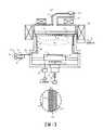
圖1,係為對於本發明之實施例的電漿處理裝置之概略構成作示意性展示之縱剖面圖。特別是,圖1(a)中所記載之本實施例之電漿處理裝置100,係身為電漿蝕刻裝置,其係在一部分為具有圓筒形狀的真空容器1之內部,具備有身為電漿15所被形成的空間之處理室7,並對於由包含有身為預先被形成於「被載置在被配置於被作了減壓的該處理室7中之試料台6之上部中央部之上面的晶圓4之上面」的上方之膜層之遮罩層的複數之膜層所構成之膜構造的身為下方之膜層的處理對象之膜層,藉由電漿15來進行蝕刻處理。FIG. 1 is a longitudinal sectional view schematically showing the schematic configuration of a plasma processing apparatus according to an embodiment of the present invention. In particular, the plasma processing apparatus 100 of this embodiment described in FIG. 1(a) is a plasma etching apparatus, which is part of a cylindrical vacuum vessel 1 with a body The
處理室7,係在上部之一部分為具有圓筒形狀的側壁部42之內側,具備有身為電漿15所被形成的空間之放電部,在處理室7內,係具備有接地構件40以及石英製之內筒41,該接地構件40,係將放電部以環狀或圓筒狀來作包圍並將側壁部42之內周壁面之下部相對於放電部而作覆蓋地作配置,該內筒41,係於接地構件40之上方處將側壁部42之內周壁面之下部相對於放電部而作覆蓋地作配置,並具備有圓筒形狀。在內筒41之上端部之上方,係被配置有石英等之介電質製之噴淋板2,該噴淋板2,係具有圓板形狀,並構成處理室7之頂面,並且於中央部處被配置有複數之處理用氣體之導入孔9。在從噴淋板2之上面起而空出有間隙8的上方處,係被配置有石英製之窗構件3,該窗構件3,係身為被載置於上端環10上之圓板狀之構件,並構成真空容器1,該上端環10,係被載置於真空容器1側壁之上端處,並為金屬製。The
圖1(b),係將圖1(a)中之虛線之圓所標示的接地構件40之其中1個場所的概略構成作擴大並作為縱剖面而示意性展示。本實施例之接地構件40,係具備有被膜140,並至少將面向處理室7並與電漿15相接觸之內周側之表面藉由此被膜140來作覆蓋,被膜140,係藉由對於從電漿15之粒子所受到的相互作用而耐性相對性而言為高的材料來構成。本實施例之接地構件40,其縱剖面係具有L字狀之形狀,並至少在內周側壁、下面以及內周側壁之上端部之上面,具備有被膜140。石英製之內筒41,係使其之下端部被載置於接地構件40之內周側壁之上端部上,並與真空容器1之具有圓筒形之上部之側壁部42的內周側壁面相互空出有間隙地而將其作覆蓋而被作配置。Fig. 1(b) is an enlarged view of the schematic configuration of one of the
另外,接地構件40之面向電漿15或與電漿15接觸的表面之面積,係具備有試料台6上之晶圓4上面之面積的2倍以上之大小。又,內筒41之具有圓筒形的內周側壁之面向電漿15或與電漿15接觸的面積,係具備有較晶圓4上面之面積而更大之值。In addition, the area of the surface of the
在本實施例中,被膜140係具備有於邊界面之上下而被層積有複數的膜層之構成,作為身為下方之膜層的基礎層,係將Y2O3作為材料,並將下層膜141以150μm之厚度來作配置。本實施例之下層膜141,係使用將具有預先所制定之組成的Y2O3之粒子以高溫之電漿來作成半熔融狀態並吹附至被覆對象之表面上的熔射法,來形成之。In this embodiment, the
在下層膜141之上面上,係將作為被混合有SiO2的以Y2O3作為主要成份之材料而具有Y2O3以及SiO2之比例=100:23(體積比)之混合比的表面膜142,以50μm之厚度來作配置。又,將被混合有SiO2之Y2O3作為材料所構成的表面膜142之Y2O3之結晶粒子尺寸,係為200nm以下,SiO2成分係主要存在於粒界中。進而,在本實施例之表面膜142中,Al、Zr、Cr、Hf、Ta、Ti以及其他之金屬,係並未被包含有1000ppm以上之量。On the upper surface of the
在身為真空容器1之窗構件3之上方的處理室7之上方處,係被連結並配置有導波管21之下端部,該導波管21,係於內部而傳播為了在處理室7之放電部內產生電漿15而被供給至處理室7內的具有2.45GHz之頻率之微波之電場。導波管21,係在其與窗構件3之間包夾有空洞部,該空洞部,係具備有與窗構件3之直徑為同值或者是近似為可視為相同之程度的直徑之圓筒形狀,於其之上方處,係具備有圓筒部,該圓筒部,係具備有較該共振部而更小之直徑且剖面為具有圓形並且其之軸為朝上下方向而延伸,在該圓筒部之上端部處,係具備有方形部,該方形部,係使其之其中一端部與圓筒部之上端部作連接,且剖面為具有矩形或方形狀,並且其之軸為延伸存在於水平方向上。在導波管21之方形部之另外一端部處,係具備有震盪並形成微波之電場的磁控管等之電源20。Above the
在導波管21之圓筒部及其之下方之空洞部以及包圍處理室7之放電部的真空容器1上部之側壁之外側處,係將此些以環狀來作包圍而在上下方向被配置有複數之線圈22、23。直流電流係被供給至於上下而成為複數(在本例中係為2)之段的線圈22、23,並產生磁場,在處理室7之內部,係被形成有具有在放電部或噴淋板2之上下方向之中心軸周圍而對稱地延伸之磁力線的磁場。At the outer side of the side wall of the upper part of the vacuum vessel 1 surrounding the cylindrical portion of the
在試料台6之內部,係具備有金屬製之基材,該金屬製之基材,係於與放電部或處理室7之上下方向之中心軸同心或者是可視為同心之程度的位置處具備有中心之軸,並具有圓板或圓筒形狀,基材係將上部之中央側之部分的高度設為較其之外周部而更高,而具有縱剖面為成為凸字狀之形狀,並在外周側具備具有階差而凹陷的環狀之凹部。被增高的中央部上面與階差部之間之上面,係藉由身為以包含氧化鋁或氧化釔之介電質之材料所構成的被膜之吸附膜,而被作覆蓋,在中央部上面之吸附膜之內部係被配置有被供給有直流電力之膜狀的電極。在將晶圓4載置於中央部上面之吸附膜上的狀態下,以對於複數之膜狀之電極而賦予各別相異之極性的方式,來供給直流電力,並將該晶圓4於下方之膜之方向上作吸附保持。Inside the sample table 6, there is a metal base material, which is provided at a position that is concentric with the center axis of the discharge part or the upper and lower directions of the
又,身為被配置在吸附膜之內部的其他之膜狀之電極之偏壓用電極或者是基材,係被與供給800MHz以下的頻率之高頻電力之高頻電源14作電性連接。高頻電源14,係經由包含有同軸纜線地所構成之供電路徑以及被配置於其上之匹配電路13地,而被與偏壓用電極作連接。在晶圓4之處理中,藉由對於偏壓電極或基材供給高頻電力,係在晶圓4之上面上方處被形成有與被形成於放電部處之電漿15之間具有電位差的偏壓電位。本實施例之高頻電源14,係對於基材或偏壓用電極而供給具備有300mm之直徑的晶圓4之每單位面積500W以下之高頻電力,藉由高頻電力所形成的高頻之偏壓電壓,係以其之振幅(Vpp)為800V以下的條件而被作使用。In addition, the bias electrode or the substrate, which is another film-shaped electrode arranged inside the adsorption film, is electrically connected to a high-
本實施例之至少一部分為具有圓筒形狀的試料台6,從上方觀察時係被配置在處理室7之水平方向之中心部處,外周之側壁係在與構成處理室7之內周側壁之真空容器1下部的側壁構件之間,藉由延伸存在有水平方向之軸的複數根之支持樑而被與真空容器1作連接。藉由此構成,試料台6係被保持於處理室7之高度方向之中央部處,在試料台6上方處,於其之上面與噴淋板2之間係被形成有放電部,在試料台6下方處,於其之底面與被配置在處理室7之底面之水平方向之中心部處的排氣開口之間,係被形成有使從放電部而來之氣體或電漿之粒子通過試料台6之外周側壁與處理室7之側壁之間的支持樑彼此間之間隙而流入的空間。At least a part of this embodiment is a sample table 6 having a cylindrical shape, which is arranged at the center of the
在真空容器1之下方,渦輪分子幫浦12係被與該真空容器1之底面作連接而被作配置,其之入口係與被配置在真空容器1內之處理室7之底面之中央部處的排氣開口相通連。渦輪分子幫浦12之出口,係藉由與旋轉幫浦等的粗略抽氣幫浦11相通連之配管而被作連接。Below the vacuum vessel 1, the
在處理室7之底部,係被配置有排氣閥16,該排氣閥16,係相對於排氣開口而於上下方向移動,並具備有在下端之位置處將排氣開口之外周作包圍而將內外氣密地密封的圓板形狀。排氣閥16,係使其之底面的外周緣部之複數之場所,與未圖示之在真空容器1底面下方處而被與該底面作了連結的致動器等之驅動裝置作連接,並藉由該驅動裝置之動作來相對於排氣開口或其之外周緣而在上下方向移動並使距離作改變,而構成為能夠對於從排氣開口而來之氣體或粒子之排氣面積可變地作調節。At the bottom of the
本實施例之電漿處理裝置100,係具備有包含此些之粗略抽氣幫浦11、渦輪分子幫浦12以及排氣閥16所構成的排氣系。在排氣閥16於排氣開口之上方而將與其之間之距離調節為特定之值的狀態下,藉由渦輪分子幫浦12以及粗略抽氣幫浦11之排氣系之動作,處理室7之試料台6下方之空間之粒子係從排氣開口而被排出至真空容器1外。The plasma processing apparatus 100 of this embodiment is provided with an exhaust system including these
於被配置在構成真空容器1上部並且至少一部分為具有圓筒形的側壁部42之上端之上方處之金屬製之上端環10處,係被連接有配管50,該配管50,係於內部而流通被導入至噴淋板2與窗構件3之間之間隙8中的處理用之氣體或惰性氣體。該配管50,係構成將處理用氣體或惰性氣體供給至處理室7內的氣體供給路徑。在本實施例中,係包含有氣體供給路徑以及處理用氣體或惰性氣體之氣體源52還有被配置在氣體供給路徑上並對於在內部而流動的氣體之流量或其速度作調節之至少1個的質量流控制器(Mass Flow Controller,MFC)等之流量調節器51地,來構成氣體供給系。A piping 50 is connected to the metal upper end ring 10, which is arranged above the upper end of the side wall 42 having a cylindrical shape and at least part of which constitutes the upper part of the vacuum vessel 1, is connected to the inside. The processing gas or inert gas introduced into the gap 8 between the shower plate 2 and the
在本實施例中,從氣體供給系而通過配管50並通過上端環10內部之貫通路徑而被導入至間隙8處的處理用之氣體或惰性氣體,係在間隙8內部擴散,之後通過複數之氣體導入孔9而被從試料台6或被載置於其之上面上而被作保持的晶圓4之上方來導入至處理室7內部。進而,藉由排氣閥16之關連於上下方向之動作以及與排氣開口之間之距離的調節,從處理室7而來之內部之氣體或粒子的排氣之量係被作調節,並構成為藉由該排氣量與從氣體供給系而通過氣體導入孔9所被供給至處理室7內部之氣體之供給量之間的平衡,而能夠將處理室7內部之壓力、特別是晶圓4上面或者是上方之放電部內之壓力調節為適於進行處理的範圍內之值。In this embodiment, the processing gas or inert gas introduced to the gap 8 from the gas supply system through the
為了檢測出處理室7內之壓力,電漿處理裝置100,係具備有被能夠與處理室7內部作通連地而配置之壓力計72。壓力計72,係與壓力偵測用之配管70相通連並被作連結,該壓力偵測用之配管70,係在處理室7之將試料台6之外側壁作包圍的內側壁處而與開口相通連,在配管70上係被配置有將該配管70之通連作開閉的閥71。在偵測出處理室7之壓力時,閥71係被開放,配管70內係成為能夠通連,在需要對於處理室7內之電漿15之粒子或在晶圓4之處理中所產生之反應生成物的到達壓力計72處之情形作抑制的情況時,閥71係被閉塞。In order to detect the pressure in the
本實施例之電漿處理裝置100,係具備有用以使該電漿處理裝置100之動作成為所期望之動作地來進行調節之未圖示之控制器,並被與渦輪分子幫浦11、粗略抽氣幫浦12、匹配電路13、高頻電源14、排氣閥16之驅動部、流量調節器51、電源20、線圈22、23、閥71、壓力計72等可通訊地作連接,而構成為受訊包含有從此些而來之資訊的訊號而檢測出動作之狀態並能夠基於其結果來發訊對於此些而下達動作之指令的訊號。進而,控制器,係構成為亦能夠進行「由電漿處理裝置100所致之晶圓4的對於處理室7之搬入以及搬出」和「晶圓4之處理的開始以及結束之檢測和下一個的晶圓4之處理之需要與否之判定」以及對此下達指令之訊號之發訊,而成為能夠對於由該電漿處理裝置100所致之動作進行調節。The plasma processing device 100 of this embodiment is equipped with a controller (not shown) that can be used to adjust the action of the plasma processing device 100 to the desired action, and is combined with the
接著,針對由本實施例之電漿處理裝置100所致的晶圓4之處理之概要作說明。並未被施加由電漿處理裝置100所致之處理的未處理之晶圓4,係於在真空容器1之外側處而被與其作了連接的身為其他之真空容器1之真空搬送容器的被作了減壓之內部之真空搬送室內,被保持於被配置在該搬送室內的機器臂處並被作搬送,而通過將真空搬送室與處理室7之間作通連的身為晶圓4用之通路之閘門,來搬入至被減壓為與真空搬送室同等之值的處理室7內。在晶圓4從機器臂之臂前端部之晶圓保持用之手而被遞交至試料台6處而臂從處理室7退出至真空搬送室處之後,閘門係藉由未圖示之開閉用之閥而被閉塞,處理室7內部係被氣密地密封。Next, the outline of the processing of the wafer 4 by the plasma processing apparatus 100 of this embodiment will be described. The unprocessed wafer 4 that has not been processed by the plasma processing apparatus 100 is attached to the vacuum transport container of another vacuum container 1 which is connected to the outside of the vacuum container 1 The vacuum transfer chamber inside the decompression chamber is held by a robot arm arranged in the transfer chamber and is transported, and the wafer that communicates between the vacuum transfer chamber and the
之後,藉由以被施加於試料台6上面之吸附膜內之膜狀之電極處的直流電力所產生之靜電力,晶圓4係被靜電吸附於該吸附膜上而被作保持,在吸附膜上面以及被保持於其之上的晶圓4之背面之間,係被供給有He等之具有熱傳導性之氣體,晶圓4與試料台6之間之熱傳導係被促進,並且,排氣閥16係朝向上方移動並被保持於上端位置處,處理室7內部係被減壓至特定之高的真空度。After that, by the electrostatic force generated by the DC power applied to the film-like electrodes in the adsorption film on the sample table 6, the wafer 4 is electrostatically attracted to the adsorption film and held. Between the upper surface of the film and the back surface of the wafer 4 held on it, a heat-conductive gas such as He is supplied. The heat conduction between the wafer 4 and the
從氣體供給系而經由流量調節器51以及配管50,處理用之氣體係被導入至處理室7中,因應於藉由壓力計72所偵測到的壓力,由排氣閥16之動作所致的排氣開口之流路面積係被調節,處理用氣體之對於處理室7的流入量和排氣開口之排氣量係取得平衡,處理室7內部之壓力係被調節為適於進行晶圓4之處理的範圍內之值。在本實施例中,處理室7內部係構成為能夠在0.1Pa~10Pa之值的範圍內而進行壓力調節。另外,在晶圓4之處理前以及處理後,處理室7係將由排氣閥16所致之排氣開口的開口度(相互之距離)設為大,並被排氣至0.01Pa以下。From the gas supply system, the gas system for processing is introduced into the
本實施例之使用有電漿之晶圓4之處理,係藉由將複數之工程持續性地實施之多步驟而被處理,在各個的步驟中,作為被導入至處理室7內之處理用之氣體,係使用至少1種類以上的包含有Cl、F、C、O、S、N、Ar、H、Br、B、He中之一種以上之元素的氣體。例如,係藉由將包含有Cl2之處理氣體供給至處理室7內並形成電漿15而對於晶圓4之處理對象之膜進行處理的步驟、使用包含有CF4之處理氣體來形成電漿15而進行處理的步驟、使用包含有O2的處理氣體來形成電漿15而進行處理的步驟、使用包含有SF6之處理氣體來形成電漿15而進行處理的步驟,來實施晶圓4之處理。The processing of the wafer 4 using plasma in this embodiment is processed by continuously implementing multiple steps of a plurality of processes, and each step is used for processing that is introduced into the
又,被膜140,係使其之表面的Ra(所謂的算數平均粗度)被設為0.5μm以上8μm以下。又,在開始用以量產半導體裝置之晶圓4之處理之前,係亦可使用導入至處理室7內的包含有氟氣之處理氣體來形成電漿15,並進行將被膜140之表面以特定之時間來曝露在該電漿15中的事先之處理,藉由此來將構成被膜140之表面的材料氟化。In addition, the
在本實施例中,作為介電質材料,被混合有SiO2之以Y2O3作為主要成分的表面膜142之組成,係如同下述一般地而被決定。亦即是,本發明者們,係將具備使用有包含Y2O3之介電質之材料的被膜之構件,配置在處理室7內部,並使用包含有SF6、O2、Ar、NF3、Cl2、CF4、CHF3之1種或2種以上的電漿15,來以特定之條件而對於晶圓4進行處理,在將此電漿處理裝置100之運轉進行了特定之期間之後,對於構成該被膜之Y2O3的結晶之粒子之體積或尺寸,使用SEM(Scanning Electron Microscope:掃描電子顯微鏡)來作調查,並與該運轉之開始前的粒子進行比較,而檢測出了粒子之膨脹的大小及其比例。In this embodiment, the composition of the
其結果,在上述之處理的條件下,Y2O3之結晶之粒子的橫方向之膨脹的比例係為7%。此事,係相當於粒子之體積作了23%的增加。基於此,本實施例之表面膜142之材料,係將構成其之Y2O3與SiO2之間之比例設為100~23(體積比)。於此,體積係指材料之結晶的粒子自身,而並不包含被形成於被膜140之內部的氣孔或間隙。本實施例之表面膜142,係根據密度而換算出會成為上述混合比的材料之各者的體積之重量,並將作為材料之Y2O3以及SiO2以會使該些之重量比成為100:10的方式來作了混合。As a result, under the conditions of the above-mentioned treatment, the ratio of the expansion in the lateral direction of the Y2 O3 crystal particles was 7%. This matter is equivalent to a 23% increase in the volume of the particle. Based on this, the material of the
藉由上述之構成,在將本實施例之於表面具備有將Y2O3和SiO2混合所形成的表面膜142之接地構件40配置於處理室7內並進行了對於晶圓4進行處理之運轉時,由於Si之成分係從表面膜142之表面而揮發並脫離,因此起因於Y2O3之粒子氟化並膨脹一事所導致的表面膜142之作為膜的尺寸增大一事係被抵消或者是降低,表面以及內部之應力的增大以及起因於該應力之增大所導致的表面膜142之表面之碎裂或缺損係被紓緩或者是被抑制。進而,若是SiO2之成分在表面膜142內部越緻密地分散存在,則係越能夠對於尺寸為更小的碎裂或缺損作抑制。在本實施例中,由於作為材料之SiO2之結晶之粒子,係存在於Y2O3之粒子彼此之間(粒界),因此係並不會發生較Y2O3之結晶之粒子的尺寸而更大之碎裂。故而,係能夠降低伴隨於碎裂所導致的異物之發生。With the above-mentioned structure, the
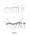
使用圖2,針對起因於陶瓷表面之應力之累積所導致的碎裂發生之機制作說明。圖2,係為對於由先前技術所致之被膜之概略構成作示意性展示之縱剖面圖。圖2(a),係為對於將在表面上被形成有被膜的內部構件配置於處理室7內並開始了對於晶圓4進行處理的運轉之初期時的被膜之縱剖面作展示之圖。又,圖2(b),係為對於在將該運轉進行了特定之值以上之期間之後的時間點處之被膜之縱剖面作展示之圖。Using Fig. 2, the mechanism for the occurrence of cracks caused by the accumulation of stress on the ceramic surface is explained. Fig. 2 is a longitudinal sectional view schematically showing the outline structure of the film produced by the prior art. FIG. 2(a) is a diagram showing a longitudinal section of the film at the initial stage of the operation of processing the wafer 4 when the internal member with the film formed on the surface is arranged in the
陶瓷材料之表面以及直到數μm之深度為止的面內方向之應力,係能夠藉由X光繞射來作調查。一般而言,由於氟係相較於氧而電負度為高,與金屬之間之結合能量係為大,因此,氧化物系陶瓷材料之表面201,係起因於面向氟電漿而使氟化有所進展,並形成包含有氟化物之變質層203。由於氧所能夠取得並安定之價數係為II,而氟係為I,因此,若是氟化,則金屬原子之1個單位的氧以及氟之合計原子數係成為增加,包含氟化物之材料的結晶之粒子以及由此所構成的變質層203係會膨脹。在實際的構件表面上,由於係並非為涵蓋全部區域而均為理想性的平面,因此,在存在有微小之凹凸的部分202處,表面係能夠膨脹。The surface of the ceramic material and the stress in the in-plane direction up to a depth of several μm can be investigated by X-ray diffraction. Generally speaking, since fluorine has a higher electronegativity than oxygen and has a greater bonding energy with metal, the
在藉由先前技術所形成之被膜的情況時,假設若是其之表面起因於氟而變質(氟化)並作了1%的膨脹,則在變質層203之正下方處,係發生未滿1%之例如0.5%的變形。陶瓷材料之楊格率多係為100GPa~400GPa之範圍,例如在楊格率為160GPa之材質的情況時,若是並未碎裂,則根據計算係成為施加有0.8GPa之拉張應力。又,表面之變質層203,雖係受到有壓縮應力,但是,陶瓷材料之壓縮強度一般而言係為拉張強度之約15倍以上,施加有拉張應力之變質層的正下方相對性而言係容易被破壞。In the case of the film formed by the prior art, if the surface is degraded (fluorinated) due to fluorine and expanded by 1%, then under the degenerated
陶瓷材料之拉張強度,係依存於結晶之缺陷或龜裂等,而多係概略為0.03GPa~1GPa之範圍。就算是表面發生變質並膨脹,在拉張應力為拉張強度以下的情況時也不會發生碎裂,但是當變形增大而拉張應力超過拉張強度時,係會產生碎裂204。若是並不存在有缺陷而拉張強度為強之場所在耐住了變形之後於該場所處發生碎裂204,則起因於應力所累積的能量係被釋放,並發生衝擊,若是朝向表面之能量係為充分,則碎裂會一直到達變質層203表面之表面處,並產生碎裂205。當能量更進一步為大的情況時,若是碎裂了的破片207從變質層203表面起朝向處理室7內部前進並再附著於晶圓4之表面上,則會成為造成污染之異物。The tensile strength of ceramic materials depends on crystal defects or cracks, and most of them are roughly in the range of 0.03GPa to 1GPa. Even if the surface undergoes deterioration and expansion, cracks will not occur when the tensile stress is below the tensile strength, but when the deformation increases and the tensile stress exceeds the tensile strength, cracks 204 will occur. If there is no defect and the tensile strength is strong, the place is broken after
此種異物,係不僅是會從上方而落下至晶圓4處,而也會有從晶圓4或是被配置在試料台6之下方處的構件表面而附著的情形。另一方面,在表面之凹凸為小而平坦的部分等之表面處,於內部所產生的拉張應力相對性而言係變小,但是,在被膜之表面處,起因於氟化一事所導致的壓縮應力係累積,若是該應力之累積程度變大,則就算是在凹凸為小的部分處,也會有產生碎裂206的可能性。Such foreign matter may not only fall to the wafer 4 from above, but may also adhere from the wafer 4 or the surface of a member arranged below the
圖3,係為對於本實施例的電漿處理裝置之被膜140之概略構成作示意性展示之縱剖面圖。圖3(a),係為對於將身為在表面上被形成有被膜的內部構件之接地構件40配置於處理室7內並開始了對於晶圓4進行處理的運轉之初期時的被膜之縱剖面作展示之圖。又,圖3(b),係為對於在將該運轉進行了特定之值以上之期間之後的時間點處之被膜140之縱剖面作展示之圖。FIG. 3 is a longitudinal sectional view schematically showing the schematic structure of the
在本實施例之表面膜142中,於圖3(a)之狀態下,身為第1材料301之SiO2之結晶粒子係分散存在於身為第2材料302之Y2O3之結晶粒子之間。在本實施例中,亦係如同圖2中所示之先前技術一般地,起因於接地構件40被配置在處理室7內部並被曝露於電漿15中,在表面膜142之表面上係被形成有包含材料之氟化物的變質層303。在本實施例中,身為第2材料302之Y2O3之結晶粒子的起因於氟化所致之體積膨脹,係藉由分散於表面膜142內的包含有SiO2之第1材料301揮發並脫離(元件符號304)一事,而使表面膜142之氟化後的變質層303內部之壓縮應力以及變質層303之正下方之拉張應力之累積被抑制,應力之累積和起因於此所導致的變質層303之表面之碎裂的產生係被作抑制。In the
另外,在熔射形成之被膜的情況時,就算是將其之表面以會成為鏡面的方式來進行研磨,亦由於在內部係存在有氣孔,因此於表面係會殘留有凹凸。故而,就算是例如施加對於表面進行研磨之加工,應力也會增加,並從凹凸而游離出起因於碎裂或缺損所導致的粒子。進而,在本實施例中,由於被膜140係被配置在接地構件40之面向處理室7內之放電部的側壁之表面處,而並非為被配置在晶圓4之正上方處者,因此,凡得瓦力為數μ以上之粒子的無法抵抗重力而使粒子落下至晶圓處的情形係被減輕。In addition, in the case of a film formed by thermal spraying, even if the surface is polished so as to be a mirror surface, since there are pores inside, unevenness remains on the surface. Therefore, even if the surface is polished, the stress increases, and particles caused by chipping or defects are released from the unevenness. Furthermore, in this embodiment, since the
在藉由熔射法所形成的本實施例之被膜140中,大部分的未固溶之SiO2係作為第2相或者是存在於Y2O3之粒界中,並相較於有所固溶之部分而較氟氣更容易揮發,將體積之膨脹作紓緩的效果係早期性地發揮。進而,在本實施例中,作為表面膜142之下層,由於係具備有以單一材料作為成分的Y2O3之下層膜141,因此係能夠對於被膜140之表面的碎裂作抑制,並且能夠使耐蝕性提升。In the
下層膜141之厚度,係亦可為100μm~200μm。為了更進一步使耐蝕性提升,當接地構件40之母材(基材)係身為鋁合金的情況時,在下層膜141之更下方處,係亦可形成氧皮鋁之層。The thickness of the
在本實施例之電漿處理裝置100中,接地構件40之基材係為金屬,其之面向處理室7之面積,係被設為晶圓面積的2倍以上之大小。其之內側壁面之壁鞘套(sheath)的電壓,係相對於藉由被供給至試料台6處之偏壓形成用之高頻電力所在晶圓4表面上產生的電壓之直流成分Vdc,而成為晶圓4面積/接地構件40之內側壁面面積之比的2.5次方。例如,當Vdc=0.5Vpp的情況時,接地構件40之內側壁面之壁鞘套的電壓通常係成為70V以下。In the plasma processing apparatus 100 of this embodiment, the base material of the
在被誘導至被形成有此種電壓的接地構件40之內壁表面上的離子等之帶電粒子發生碰撞時的離子能量中,由於身為構成由濺鍍所致之被膜140的第2材料302之Y2O3的消耗係為小,因此,可以推測到,係並不會有「在SiO2從表面膜142而脫離之後的孔(pit)之內部,電漿15中之帶電粒子發生碰撞並以該孔作為起點而顯著地被濺鍍有Y2O3」的情形。又,起因於Y之被作了濺鍍的原子累積在其他場所處一事所導致的異物或歷時變化係為少。熔射,係較為易於成膜氧化物之混合物。In the ion energy induced when the charged particles such as ions on the inner wall surface of the grounding
又,藉由熔射所形成的被膜140之表面,由於係並非身為像是對於燒結材作了研磨後一般的鏡面,因此,就算是起因於Si等之揮發、脫離而產生有凹部,該凹部之尺寸亦係相較於被膜140之表面之凹凸的大小而為充分小。進而,由於被膜140係並未將Al作1000ppm以上之含有,因此起因於Al而導致的晶圓4或處理室7內表面之污染係被降低。又,在使用包含有氯的氣體而形成電漿15並對於晶圓4進行處理之步驟中,被膜140之材料係成為AlCl3、Al2Cl6、YAlCl6等之氯化物,對於電漿而具有耐性的成分被化學性消耗的情形係被降低。另外,若依據發明者們之檢討,則係得知了,在包含有形成使用有包含氟元素之氣體的電漿15之工程的晶圓4之電漿處理中,就算是以各種的氣體種類而放電,也不會有氟化物(包含氟氧化物)恢復至原本之氧化物的情形。In addition, the surface of the
在本實施例之電漿處理裝置100中的晶圓4之處理之條件,係晶圓4之處理中的處理室7內之壓力為0.1Pa~10Pa。因此,具備有此以上的蒸氣壓或昇華壓之物質,在閥16被開啟而排氣系為有所動作的晶圓4之處理中,亦係被有效地排氣。在本實施例中,身為構成表面膜142之上層之變質層303的材料之Si,係作為物質而揮發,在以Si作為材料的晶圓4以及包含有其之上面之處理對象之膜的膜構造處而發生污染的情形係被降低。The conditions for the processing of the wafer 4 in the plasma processing apparatus 100 of this embodiment are that the pressure in the
又,作為內筒41或在試料台6上部之晶圓4所被作載置的上面之外周側處而將其作包圍地所配置之對試料台6作保護的環等處,由於作為材料係使用有石英,因此起因於作為物質之Si被放出一事所導致的對於晶圓4表面或處理條件之影響係成為充分小。進而,在被膜140之表面膜142中,Ti、Cr、Zr、Zn、Hf、Ta等之材料,係並未被包含有1000ppm以上之量。因此,此些之物質成為蒸氣壓為低之氟化物並殘留於處理室7內部而再度附著於晶圓4處並造成污染的情形係被降低。In addition, as the
本實施例之被膜140,係亦被形成於接地構件40以外的被配置在處理室7之內部並具有面向電漿15或者是曝露並作接觸的表面之其他之構件處,而同樣的能夠發揮保護構件之母材(基材)免於受到由電漿15之帶電粒子或反應性為高之粒子所導致的攻擊和對於由該被膜140之變質所致的對於晶圓4之污染作降低、抑制的作用、效果。作為成膜被膜140之方法,除了APS法之外,係亦能夠使用就算是對於100nm以下之粒子的細微度並且熔點為大幅度相異之材質也能夠進行成膜的氣膠沈積法、能夠使用100nm以下之粒子之原料的懸浮電漿熔射等。藉由使用此些之方法,第1材質和第2材質不論是在膜形成前或者是形成後的材料內均係更均勻地分布,藉由此,係能夠對於更小的碎裂以及起因於此之更小的異物之產生作抑制。The
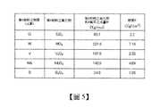
接著,使用圖4以及圖5,針對在上述實施例之電漿處理裝置100中的被使用於被膜140之表面膜142處的材料之組合之例作說明。圖4,係為對於構成圖1中所示之本實施例之電漿處理裝置之被膜的材料中之相對於氧化物與氟化物乃為非揮發性之複數之第2材料的將具有揮發性之第1材料作混合之量的適當之範圍作展示之表。圖5,係為對於身為圖4中所示之第1材料並且具有揮發性的氟化物係會成為較特定之處理室內之壓力而更大的蒸氣壓之複數之第1材料的物理性質作展示之表。Next, using FIGS. 4 and 5, an example of the combination of materials used at the
上述實施例之構成被膜140之表面膜142的第1以及第2材料,係根據被混合之此些的材料之物理性質,來決定其混合比。針對第1材料係為Y2O3、第2材料係為SiO2的情況,來進行說明。The mixing ratio of the first and second materials constituting the
圖4之第2行,係對於作為第1材料而被使用的物質(元素)名稱為「Y」的情況作展示。於此情況,作為被熔射形成之表面膜142之第2材料,係使用氧化物Y2O3,氟化物係為YF3。在假設Y2O3完全氟化並變化為YF3的情況時,可以得知在1個的Y元素處係概略發生有61%的體積增加。此些係能夠根據氧化物之莫耳體積和氟化物之莫耳體積以及此些之化學式而算出之。The second row of Fig. 4 shows the case where the name of the substance (element) used as the first material is "Y". In this case, as the second material of the
另一方面,依存於使用有含氟電漿和氧電漿之晶圓4之處理的條件,表面膜142之表面的材料係會有並未完全被氟化而成為氟氧化物的情況。例如,在Y2O3的情況時,係會有變化為Y5O4F7的情形。於此情況,可以算出在1個的Y元素處係發生有11%的體積增加,此係為完全氟化的情況時之體積增加比例的約0.18倍。On the other hand, depending on the processing conditions of the wafer 4 using fluorine-containing plasma and oxygen plasma, the surface material of the
氟化,係從氧化物之全部的氧中之一部分被置換為氟起而開始,但是,由於若是在1個的金屬原子處而氟所結合的個數越增加,則在更進一步氟化時的結合能量係會變得越小,因此氟化的進展係逐漸變慢。在膨脹並導致壓縮應力變高的表面處,進展係更進一步變慢,在完全氟化之前,進展係實質性地停止。於此情況,若依據發明者們之檢討,則在上述之實施例中,由氟化所致之堆積的增加比例,係為表面膜142之表面的第2材料完全氟化的情況時之約0.37倍。Fluorination starts when a part of all oxygen in the oxide is replaced with fluorine. However, as the number of bonded fluorine increases at one metal atom, further fluorination occurs. The binding energy of fluorine will become smaller, so the progress of fluorination will gradually slow down. At the surface where the expansion leads to a higher compressive stress, the progression slows down even further, and the progression stops substantially before the complete fluorination. In this case, according to the review of the inventors, in the above-mentioned embodiment, the increase rate of the accumulation caused by fluorination is approximately the case when the second material on the surface of the
根據此,在本實施例中,作為將身為第1材料之SiO2和身為第2材料之Y2O3作混合之比例,係選擇根據第2材料之元素完全成為了氟化物的情況時之計算所求取出的體積之增加之比例的0.18倍~0.4倍之範圍內者。若是身為此範圍內之混合的比例(比),則可以推測到,氟化所進展的能量係適度地降低並與對於氟化之進展作抑制的表面之壓縮應力相抗衡並安定,藉由此,碎裂的情形係被作抑制。另一方面,在SiO2之比例為較此範圍而更少的情況時,由Y2O3之氟化膨脹所致的內部之拉張應力或表層之壓縮應力係變大,發生碎裂或脫粒的可能性係變高。Based on this, in this embodiment, as the mixing ratio of SiO2 as the first material and Y2 O3 as the second material, the selection is based on the case where the element of the second material is completely fluoride The calculation of time is within the range of 0.18 times to 0.4 times of the increase ratio of the volume taken out. If it is the mixing ratio (ratio) within this range, it can be inferred that the energy developed by fluorination is moderately reduced, and the compressive stress of the surface that inhibits the progress of fluorination is counterbalanced and stabilized. Therefore, the fragmentation is suppressed. On the other hand, when the ratio of SiO2 is less than this range, the internal tensile stress or the compressive stress of the surface layer caused by the fluorination expansion of Y2 O3 becomes larger, and chipping or The possibility of threshing is higher.
又,在晶圓4之處理的條件中,表面膜142之第1材料會成為完全氟化的狀態之第1材料之量,係身為作混合之量的上限。若是混入此以上的第1材料,則就算是氟化並發生有體積的膨脹,亦由於更多的體積係會揮發,因此會產生有間隙。In addition, in the processing conditions of the wafer 4, the amount of the first material of the
在被混合的材料中之第1以及第2材料之重量的比例,係能夠根據圖4以及圖5中所示之數值來基於下式而求取之。The weight ratio of the first and second materials among the materials to be mixed can be calculated based on the following formula based on the numerical values shown in FIGS. 4 and 5.
第2材料之氧化物量:第1材料之氧化物量=A:(A/B×第1材料之氧化物之混合量(將第2材料之氧化物之體積設為100))×C於此,(圖4 A=圖4之第2材料之氧化物的1莫耳之氧化物之式量B=圖4之第2材料之氧化物之密度第1材料之氧化物之混合量(將第2材料之氧化物之體積設為100)為在圖4中,圖5 C=第1材料之氧化物之密度)。The amount of oxide of the second material: the amount of oxide of the first material =A: (A/B×the mixed amount of the oxide of the first material (set the volume of the oxide of the second material to 100))×CHere,(Figure 4 A = the formula of 1 mol of oxide of the second material in Figure 4B=The density of the oxide of the second material in Figure 4The mixing amount of the oxide of the first material (set the volume of the oxide of the second material as 100) is shown in Figure 4,Figure 5 C=The density of the oxide of the first material).
根據物理性質值來制定表面膜142之第1、第2材料之被混合之比例的上述之方法,在此些之材料為圖4、5中所示之其他種類之物質(元素)的情況時,係亦可同樣作適用。例如,在將第2材料設為Yb2O3,並將第1材料設為WO2的情況時,係可將氧化物之混合之比例,以體積比來制定為Yb2O3:WO2=100:6。又,根據上式,材料之重量比係可設為Yb2O3:WO2=197:9。The above-mentioned method of determining the mixing ratio of the first and second materials of the
藉由此情況之材料所構成的被膜140,亦同樣的,當在藉由上述之實施例之電漿處理裝置100所實施的晶圓4之處理中,藉由處理室7內之包含氟之氣體種類和壓力之條件所形成的WF6係從表面膜142而揮發,而能夠紓緩起因於由Yb2O3之氟化所導致的結晶之粒子之體積之增大所造成的表面膜142或其之氟化後的變質層303之尺寸的增大,表面膜142之表面的碎裂或異物之發生係被作抑制。在本例的情況時,由於第2材料之原子量係為大而接近第1原子,因此係能夠期待有相對於從電漿15而來之離子之射入的濺鍍耐性之提升。The
就算是身為圖5中所示者以外的元素,亦同樣的,在像是Cr、Ir、Hf、Nb、Ta等之蒸氣壓或昇華壓為較在電漿處理裝置100之晶圓4之處理中的處理室7內之壓力而更高的情況時,由於係能夠從被膜140之表面而揮發,並且氟化物之強度亦相對性而言係為小,因此在表面膜142內部,應力係不會累積,而有著防止碎裂的效果。例如,當預先被形成於晶圓4之上面處的用以形成半導體裝置之電路構造之膜構造的處理對象之膜為包含有Ti、Hf、Ta之至少其中一者的情況時,係亦可在表面膜142中將此些之元素作為第1材料而包含之。Even if it is an element other than the one shown in Figure 5, the same is true for the vapor pressure or sublimation pressure of Cr, Ir, Hf, Nb, Ta, etc., compared to the wafer 4 in the plasma processing apparatus 100 When the pressure in the
又,作為非揮發性之第2材料,就算是使用由圖4之複數之元素及/或其他之3A族所成之氧化物,也能夠發揮與上述實施例相同的作用、效果。又,就算是作為具有揮發性之第2材料而將相同特性之複數之元素作混合,也能夠發揮相同的效果。In addition, as the non-volatile second material, even if it uses the plural elements of FIG. 4 and/or other oxides of group 3A, the same functions and effects as the above-mentioned embodiment can be exerted. In addition, even if it is a second material with volatility, it is possible to have the same effect by mixing plural elements with the same characteristics.
又,在上述實施例中,雖係針對在被配置於處理室7內部之接地構件40等的構件之面向電漿15之表面處所被配置的被膜140,來作了說明,但是,就算是對於構成作為燒結體而被形成的陶瓷構件之表面的場所處,而適用將上述第1、第2材料作了混合之材料,亦能夠發揮相同的作用、效果。又,作為第1以及第2材料,或者是作為表面膜142之材料,係並不被限定於陶瓷材,就算是玻璃等之其他之氧化物的材料,也能夠發揮相同的效果。In addition, in the above-mentioned embodiment, although the
另外,本發明係並不被限定於上述之實施例,而亦包含有各種的變形例。例如,上述之實施例,係為為了對於本發明作易於理解之說明而作了詳細說明者,本發明係並不被限定於與所作了說明的全部之使用條件相同之構成者。又,亦可將某一實施例之構成的一部分置換為其他實施例之構成。又,係並不被限定於在實施例中所列舉的例子之比例。In addition, the present invention is not limited to the above-mentioned embodiments, but includes various modifications. For example, the above-mentioned embodiments are described in detail for the purpose of explaining the present invention easily, and the present invention is not limited to those having the same configuration as all the described usage conditions. In addition, a part of the configuration of a certain embodiment may be replaced with the configuration of another embodiment. In addition, the system is not limited to the ratio of the examples cited in the examples.
1:真空容器2:噴淋板3:窗構件4:晶圓6:試料台7:處理室8:間隙9:氣體導入孔11:粗略抽氣幫浦12:渦輪分子幫浦13:匹配電路14:高頻電源15:電漿16:閥20:電源21:導波管22,23:線圈40:接地構件41:內筒42:側壁構件100:電漿處理裝置140:被膜141:下層膜142:表面膜1: Vacuum container2: Spray board3: Window components4: Wafer6: sample table7: Processing room8: gap9: Gas inlet11: Roughly pump the pump12: Turbomolecular pump13: matching circuit14: High frequency power supply15: Plasma16: valve20: Power21: Stillpipe22, 23: coil40: Grounding member41: inner cylinder42: side wall member100: Plasma processing device140: envelope141: Underlayer film142: Surface film
[圖1]係為對於本發明之實施例的電漿處理裝置之概略構成作示意性展示之縱剖面圖。[圖2]係為對於由先前技術所致之被膜之概略構成作示意性展示之縱剖面圖。[圖3]係為對於圖1中所示之本實施例的電漿處理裝置所具備之被膜之概略構成作示意性展示之縱剖面圖。[圖4]係為對於構成圖1中所示之本實施例之電漿處理裝置之被膜的材料中之相對於氧化物與氟化物乃為非揮發性之複數之第2材料的將具有揮發性之第1材料作混合之量的適當之範圍作展示之表。[圖5]係為對於身為圖4中所示之第1材料並且具有揮發性的氟化物係會成為較特定之處理室內之壓力而更大的蒸氣壓之複數之第1材料的物理性質作展示之表。Fig. 1 is a longitudinal sectional view schematically showing the schematic configuration of a plasma processing apparatus according to an embodiment of the present invention.[Figure 2] is a longitudinal cross-sectional view schematically showing the outline composition of the film produced by the prior art.[Fig. 3] is a longitudinal cross-sectional view schematically showing the schematic structure of the coating film provided in the plasma processing apparatus of the present embodiment shown in Fig. 1. [Fig.[FIG. 4] It shows that the second material which is the plural non-volatile with respect to oxide and fluoride among the materials constituting the film of the plasma processing apparatus of the present embodiment shown in FIG. 1 will have volatilization The first material of sex is used as a table showing the proper range of mixing amount.[Figure 5] It is the physical properties of the first material that is the first material shown in Figure 4 and has a volatile fluoride system that has a higher vapor pressure than the pressure in the specific processing chamber Make a display table.
1:真空容器1: Vacuum container
2:噴淋板2: Spray board
3:窗構件3: Window components
4:晶圓4: Wafer
6:試料台6: sample table
7:處理室7: Processing room
8:間隙8: gap
9:氣體導入孔9: Gas inlet
11:粗略抽氣幫浦11: Roughly pump the pump
12:渦輪分子幫浦12: Turbomolecular pump
13:匹配電路13: matching circuit
14:高頻電源14: High frequency power supply
15:電漿15: Plasma
16:閥16: valve
18,20:電源18, 20: Power
21:導波管21: Stillpipe
22,23:線圈22, 23: coil
40:接地構件40: Grounding member
41:內筒41: inner cylinder
50:配管50: Piping
51:流量調節器51: flow regulator
70:配管70: Piping
71:閥71: Valve
72:壓力計72: Pressure gauge
140:被膜140: envelope
141:下層膜141: Underlayer film
142:表面膜142: Surface film
Claims (9)
Translated fromChineseApplications Claiming Priority (2)
| Application Number | Priority Date | Filing Date | Title |
|---|---|---|---|
| WOPCT/JP2019/015912 | 2019-04-12 | ||
| PCT/JP2019/015912WO2020208801A1 (en) | 2019-04-12 | 2019-04-12 | Plasma processing device, internal member for plasma processing device, and method for manufacturing said internal member |
Publications (1)
| Publication Number | Publication Date |
|---|---|
| TW202037737Atrue TW202037737A (en) | 2020-10-16 |
Family
ID=72751170
Family Applications (1)
| Application Number | Title | Priority Date | Filing Date |
|---|---|---|---|
| TW109106867ATW202037737A (en) | 2019-04-12 | 2020-03-03 | Plasma processing device, internal member for plasma processing device, and method for manufacturing said internal member |
Country Status (6)
| Country | Link |
|---|---|
| US (1) | US20210241998A1 (en) |
| JP (1) | JPWO2020208801A1 (en) |
| KR (1) | KR20200120601A (en) |
| CN (1) | CN112088424A (en) |
| TW (1) | TW202037737A (en) |
| WO (1) | WO2020208801A1 (en) |
Cited By (1)
| Publication number | Priority date | Publication date | Assignee | Title |
|---|---|---|---|---|
| CN114059000A (en)* | 2020-12-10 | 2022-02-18 | Komico有限公司 | Yttrium-based particle powder for thermal spraying, yttrium-based particles, and methods for producing these |
Families Citing this family (1)
| Publication number | Priority date | Publication date | Assignee | Title |
|---|---|---|---|---|
| KR102266655B1 (en)* | 2020-12-10 | 2021-06-18 | (주)코미코 | The method of producing thermal spray coating using the yittrium powder and the yittrium coating produced by the mothod |
Family Cites Families (7)
| Publication number | Priority date | Publication date | Assignee | Title |
|---|---|---|---|---|
| US5680013A (en)* | 1994-03-15 | 1997-10-21 | Applied Materials, Inc. | Ceramic protection for heated metal surfaces of plasma processing chamber exposed to chemically aggressive gaseous environment therein and method of protecting such heated metal surfaces |
| JP2003264169A (en)* | 2002-03-11 | 2003-09-19 | Tokyo Electron Ltd | Plasma treatment device |
| JP4351980B2 (en)* | 2004-09-16 | 2009-10-28 | 株式会社日立ハイテクノロジーズ | Plasma processing method |
| JP2007321183A (en)* | 2006-05-31 | 2007-12-13 | Nihon Ceratec Co Ltd | Plasma-resistant material |
| US20100055298A1 (en)* | 2008-08-28 | 2010-03-04 | Applied Materials, Inc. | Process kit shields and methods of use thereof |
| US8206829B2 (en)* | 2008-11-10 | 2012-06-26 | Applied Materials, Inc. | Plasma resistant coatings for plasma chamber components |
| JP2012222225A (en)* | 2011-04-12 | 2012-11-12 | Hitachi High-Technologies Corp | Plasma processing equipment |
- 2019
- 2019-04-12USUS16/646,917patent/US20210241998A1/ennot_activeAbandoned
- 2019-04-12CNCN201980004282.3Apatent/CN112088424A/enactivePending
- 2019-04-12WOPCT/JP2019/015912patent/WO2020208801A1/ennot_activeCeased
- 2019-04-12JPJP2020512750Apatent/JPWO2020208801A1/enactivePending
- 2019-04-12KRKR1020207004956Apatent/KR20200120601A/ennot_activeAbandoned
- 2020
- 2020-03-03TWTW109106867Apatent/TW202037737A/enunknown
Cited By (1)
| Publication number | Priority date | Publication date | Assignee | Title |
|---|---|---|---|---|
| CN114059000A (en)* | 2020-12-10 | 2022-02-18 | Komico有限公司 | Yttrium-based particle powder for thermal spraying, yttrium-based particles, and methods for producing these |
Also Published As
| Publication number | Publication date |
|---|---|
| CN112088424A (en) | 2020-12-15 |
| US20210241998A1 (en) | 2021-08-05 |
| JPWO2020208801A1 (en) | 2021-05-06 |
| KR20200120601A (en) | 2020-10-21 |
| WO2020208801A1 (en) | 2020-10-15 |
Similar Documents
| Publication | Publication Date | Title |
|---|---|---|
| TWI778245B (en) | Plasma processing apparatus and member for plasma processing apparatus, and method for producing plasma processing apparatus and method for producing member for plasma processing apparatus | |
| US6656535B2 (en) | Method of fabricating a coated process chamber component | |
| JP6034156B2 (en) | Plasma processing apparatus and plasma processing method | |
| EP1405330B1 (en) | Process chamber components having textured internal surfaces and method of manufacture | |
| EP1847628B1 (en) | Conductive, plasma-resistant member | |
| US20120216955A1 (en) | Plasma processing apparatus | |
| CN112779488A (en) | Yttrium fluoride spray coating, spray material for the same, and corrosion-resistant coating including the spray coating | |
| WO2002079538A1 (en) | Cerium oxide containing ceramic components and coatings in semiconductor processing equipment | |
| US20070215283A1 (en) | Plasma treating apparatus and plasma treating method | |
| CN111247627B (en) | Component for plasma etching device with improved plasma resistance and method for manufacturing the same | |
| JP2008526026A (en) | Method and structure for reducing byproduct deposition in plasma processing systems | |
| TW202037737A (en) | Plasma processing device, internal member for plasma processing device, and method for manufacturing said internal member | |
| CN100381390C (en) | Plasma resistant components | |
| WO2022009340A1 (en) | Cover member for plasma processing device, plasma processing, and membrane production method | |
| TWI420588B (en) | Plasma etching method | |
| US7488689B2 (en) | Plasma etching method | |
| US20060157198A1 (en) | Member for plasma processing apparatus and plasma processing apparatus | |
| US10100413B2 (en) | Component for plasma apparatus and method of manufacturing the same | |
| CN119923706A (en) | Grounding device for substrate processing chamber | |
| WO2025027694A1 (en) | Member for plasma treatment apparatus and method for manufacturing same | |
| JP2005311120A (en) | Inductively-coupled plasma generator and dry etching system using it |