TW202032187A - Real-number photonic encoding - Google Patents
Real-number photonic encodingDownload PDFInfo
- Publication number
- TW202032187A TW202032187ATW108116586ATW108116586ATW202032187ATW 202032187 ATW202032187 ATW 202032187ATW 108116586 ATW108116586 ATW 108116586ATW 108116586 ATW108116586 ATW 108116586ATW 202032187 ATW202032187 ATW 202032187A
- Authority
- TW
- Taiwan
- Prior art keywords
- optical
- phase
- matrix
- signal
- modulator
- Prior art date
Links
- 230000003287optical effectEffects0.000claimsabstractdescription549
- 238000000034methodMethods0.000claimsabstractdescription115
- 230000001427coherent effectEffects0.000claimsabstractdescription52
- 230000009466transformationEffects0.000claimsabstractdescription30
- 238000004891communicationMethods0.000claimsabstractdescription13
- 238000012545processingMethods0.000claimsdescription92
- 238000006243chemical reactionMethods0.000claimsdescription47
- 238000004519manufacturing processMethods0.000claimsdescription29
- 239000000758substrateSubstances0.000claimsdescription29
- 239000013307optical fiberSubstances0.000claimsdescription19
- 238000002156mixingMethods0.000claimsdescription13
- 239000004065semiconductorSubstances0.000claimsdescription11
- 230000001131transforming effectEffects0.000claimsdescription9
- 230000008878couplingEffects0.000claimsdescription8
- 238000010168coupling processMethods0.000claimsdescription8
- 238000005859coupling reactionMethods0.000claimsdescription8
- 238000013507mappingMethods0.000claimsdescription4
- 238000005259measurementMethods0.000abstractdescription24
- 238000001514detection methodMethods0.000abstractdescription20
- 238000010801machine learningMethods0.000abstractdescription6
- 239000011159matrix materialSubstances0.000description357
- 239000013598vectorSubstances0.000description136
- 230000010363phase shiftEffects0.000description31
- 230000000670limiting effectEffects0.000description27
- 238000010586diagramMethods0.000description25
- 238000004364calculation methodMethods0.000description23
- 238000000354decomposition reactionMethods0.000description13
- 230000008569processEffects0.000description13
- 230000004044responseEffects0.000description13
- 230000003595spectral effectEffects0.000description13
- 230000008859changeEffects0.000description10
- 230000008901benefitEffects0.000description8
- 238000003491arrayMethods0.000description7
- 230000006870functionEffects0.000description7
- 239000000463materialSubstances0.000description7
- 238000000844transformationMethods0.000description6
- 230000000694effectsEffects0.000description5
- 238000005516engineering processMethods0.000description5
- 230000001902propagating effectEffects0.000description5
- 238000005070samplingMethods0.000description5
- 238000011896sensitive detectionMethods0.000description5
- XUIMIQQOPSSXEZ-UHFFFAOYSA-NSiliconChemical compound[Si]XUIMIQQOPSSXEZ-UHFFFAOYSA-N0.000description4
- 230000005684electric fieldEffects0.000description4
- 239000000835fiberSubstances0.000description4
- 229910052710siliconInorganic materials0.000description4
- 239000010703siliconSubstances0.000description4
- 238000012549trainingMethods0.000description4
- 230000000007visual effectEffects0.000description4
- 230000002238attenuated effectEffects0.000description3
- 230000006399behaviorEffects0.000description3
- 230000008033biological extinctionEffects0.000description3
- 229940050561matrix productDrugs0.000description3
- 230000011218segmentationEffects0.000description3
- 238000012360testing methodMethods0.000description3
- 230000005540biological transmissionEffects0.000description2
- 238000009529body temperature measurementMethods0.000description2
- 239000000470constituentSubstances0.000description2
- 230000001419dependent effectEffects0.000description2
- 238000013461designMethods0.000description2
- 230000006872improvementEffects0.000description2
- 230000002452interceptive effectEffects0.000description2
- 238000012986modificationMethods0.000description2
- 230000004048modificationEffects0.000description2
- 230000000644propagated effectEffects0.000description2
- 230000002829reductive effectEffects0.000description2
- 229920006395saturated elastomerPolymers0.000description2
- 230000006641stabilisationEffects0.000description2
- 238000011105stabilizationMethods0.000description2
- 230000003068static effectEffects0.000description2
- 238000012546transferMethods0.000description2
- 229910002601GaNInorganic materials0.000description1
- 229910001218Gallium arsenideInorganic materials0.000description1
- 229910000530Gallium indium arsenideInorganic materials0.000description1
- 230000005699Stark effectEffects0.000description1
- 238000010521absorption reactionMethods0.000description1
- 230000001133accelerationEffects0.000description1
- 238000004458analytical methodMethods0.000description1
- 238000013528artificial neural networkMethods0.000description1
- 238000010009beatingMethods0.000description1
- 230000009286beneficial effectEffects0.000description1
- 230000000903blocking effectEffects0.000description1
- 239000003990capacitorSubstances0.000description1
- 150000001875compoundsChemical class0.000description1
- -1concentration)Chemical class0.000description1
- 238000007796conventional methodMethods0.000description1
- 238000013527convolutional neural networkMethods0.000description1
- 238000012937correctionMethods0.000description1
- 239000013078crystalSubstances0.000description1
- 238000007405data analysisMethods0.000description1
- 230000003247decreasing effectEffects0.000description1
- 230000008021depositionEffects0.000description1
- 239000006185dispersionSubstances0.000description1
- RDYMFSUJUZBWLH-UHFFFAOYSA-NendosulfanChemical compoundC12COS(=O)OCC2C2(Cl)C(Cl)=C(Cl)C1(Cl)C2(Cl)ClRDYMFSUJUZBWLH-UHFFFAOYSA-N0.000description1
- 230000007613environmental effectEffects0.000description1
- 238000005530etchingMethods0.000description1
- 238000012804iterative processMethods0.000description1
- 239000004973liquid crystal related substanceSubstances0.000description1
- GQYHUHYESMUTHG-UHFFFAOYSA-Nlithium niobateChemical compound[Li+].[O-][Nb](=O)=OGQYHUHYESMUTHG-UHFFFAOYSA-N0.000description1
- 238000007726management methodMethods0.000description1
- 230000000873masking effectEffects0.000description1
- 239000000203mixtureSubstances0.000description1
- 230000008520organizationEffects0.000description1
- 230000036961partial effectEffects0.000description1
- 239000004038photonic crystalSubstances0.000description1
- 238000002360preparation methodMethods0.000description1
- 230000008672reprogrammingEffects0.000description1
- 230000000717retained effectEffects0.000description1
- 238000012552reviewMethods0.000description1
- 238000010079rubber tappingMethods0.000description1
- 238000000926separation methodMethods0.000description1
- 238000001228spectrumMethods0.000description1
- 238000003860storageMethods0.000description1
- 239000000126substanceSubstances0.000description1
- 230000002277temperature effectEffects0.000description1
- 230000036962time dependentEffects0.000description1
- 238000002834transmittanceMethods0.000description1
- 238000013024troubleshootingMethods0.000description1
Images


Classifications
- H—ELECTRICITY
- H03—ELECTRONIC CIRCUITRY
- H03M—CODING; DECODING; CODE CONVERSION IN GENERAL
- H03M5/00—Conversion of the form of the representation of individual digits
- H03M5/02—Conversion to or from representation by pulses
- H—ELECTRICITY
- H04—ELECTRIC COMMUNICATION TECHNIQUE
- H04B—TRANSMISSION
- H04B10/00—Transmission systems employing electromagnetic waves other than radio-waves, e.g. infrared, visible or ultraviolet light, or employing corpuscular radiation, e.g. quantum communication
- H04B10/25—Arrangements specific to fibre transmission
- H—ELECTRICITY
- H04—ELECTRIC COMMUNICATION TECHNIQUE
- H04B—TRANSMISSION
- H04B10/00—Transmission systems employing electromagnetic waves other than radio-waves, e.g. infrared, visible or ultraviolet light, or employing corpuscular radiation, e.g. quantum communication
- H04B10/50—Transmitters
- H04B10/516—Details of coding or modulation
- H04B10/524—Pulse modulation
- H—ELECTRICITY
- H04—ELECTRIC COMMUNICATION TECHNIQUE
- H04L—TRANSMISSION OF DIGITAL INFORMATION, e.g. TELEGRAPHIC COMMUNICATION
- H04L27/00—Modulated-carrier systems
- H04L27/02—Amplitude-modulated carrier systems, e.g. using on-off keying; Single sideband or vestigial sideband modulation
- H—ELECTRICITY
- H04—ELECTRIC COMMUNICATION TECHNIQUE
- H04L—TRANSMISSION OF DIGITAL INFORMATION, e.g. TELEGRAPHIC COMMUNICATION
- H04L27/00—Modulated-carrier systems
- H04L27/02—Amplitude-modulated carrier systems, e.g. using on-off keying; Single sideband or vestigial sideband modulation
- H04L27/04—Modulator circuits; Transmitter circuits
- H—ELECTRICITY
- H04—ELECTRIC COMMUNICATION TECHNIQUE
- H04L—TRANSMISSION OF DIGITAL INFORMATION, e.g. TELEGRAPHIC COMMUNICATION
- H04L27/00—Modulated-carrier systems
- H04L27/32—Carrier systems characterised by combinations of two or more of the types covered by groups H04L27/02, H04L27/10, H04L27/18 or H04L27/26
- H04L27/34—Amplitude- and phase-modulated carrier systems, e.g. quadrature-amplitude modulated carrier systems
Landscapes
- Engineering & Computer Science (AREA)
- Computer Networks & Wireless Communication (AREA)
- Signal Processing (AREA)
- Physics & Mathematics (AREA)
- Electromagnetism (AREA)
- Theoretical Computer Science (AREA)
- Optical Modulation, Optical Deflection, Nonlinear Optics, Optical Demodulation, Optical Logic Elements (AREA)
- Optical Communication System (AREA)
Abstract
Description
Translated fromChinese對於相關申請案的交互參照:本申請案根據專利法第28條之規定,主張對於申請於2018年6月4日、名為「Photonic Processing Systems and Methods」的美國臨時申請案第62/680,557號的優先權,在此仰賴且併入此美國臨時申請案之內容以作為參考。Cross-reference to related applications: This application is based on the provisions of Article 28 of the Patent Law, claiming to be applied to the US Provisional Application No. 62/680,557 named "Photonic Processing Systems and Methods" on June 4, 2018 The priority of, depends on and incorporates the content of this US provisional application for reference.
本申請案根據專利法第28條之規定,主張對於申請於2018年11月11日、名為「REAL NUMBER PHOTONIC ENCODING」的美國臨時申請案第62/755,402號的優先權,在此仰賴且併入此美國臨時申請案之內容以作為參考。In accordance with Article 28 of the Patent Law, this application claims priority to the U.S. Provisional Application No. 62/755,402 filed on November 11, 2018 and named "REAL NUMBER PHOTONIC ENCODING". The content of this US provisional application is included for reference.
本揭示內容涉及用於在光域中編碼實數的方法和系統。The present disclosure relates to methods and systems for encoding real numbers in the optical domain.
光線性變換對於包括計算在內的許多應用變得越來越重要。可以使用光處理器(例如光子電路)來執行這種線性變換。Light linear transformation is becoming more and more important for many applications including computing. An optical processor (such as a photonic circuit) can be used to perform this linear transformation.
一些實施例相關於一種光子系統,包含:調變器,調變器經配置為由單個電調變信號驅動;相干接收器;以及光學變換單元,光學變換單元光耦合在調變器與相干接收器之間。Some embodiments are related to an optical subsystem, including: a modulator configured to be driven by a single electrical modulation signal; a coherent receiver; and an optical conversion unit that is optically coupled between the modulator and the coherent receiver Between the devices.
在一些具體實施例中,光子系統進一步包含電編碼器,電編碼器經配置以將有號實數編碼到單個電調變信號上。In some specific embodiments, the optical subsystem further includes an electrical encoder configured to encode a signed real number onto a single electrical modulation signal.
在一些具體實施例中,調變器、相干接收器與光學變換單元被設置在共同半導體基板上。In some specific embodiments, the modulator, the coherent receiver, and the optical conversion unit are arranged on a common semiconductor substrate.
在一些具體實施例中,調變器經配置以基於單個電調變信號,根據開關鍵控(OOK)調變方案來調變光輸入信號。In some embodiments, the modulator is configured to modulate the optical input signal according to an on-off keying (OOK) modulation scheme based on a single electrical modulation signal.
在一些具體實施例中,調變器經配置以基於單個電調變信號,來調變光輸入信號的強度與相位。In some embodiments, the modulator is configured to modulate the intensity and phase of the optical input signal based on a single electrical modulation signal.
在一些具體實施例中,調變器經配置以將單個電調變信號賦予到光輸入信號的強度上。In some embodiments, the modulator is configured to impart a single electrical modulation signal to the intensity of the optical input signal.
在一些具體實施例中,調變器經配置以輸出調變光學信號與參考信號,參考信號包含光載波,且其中相干接收器經配置以由參考信號打擊調變光學信號,如由光學變換單元變換。In some embodiments, the modulator is configured to output a modulated optical signal and a reference signal, the reference signal includes an optical carrier, and the coherent receiver is configured to modulate the optical signal by the reference signal, such as by an optical conversion unit Transform.
在一些具體實施例中,相干接收器包含本地震盪器與光偵測器。In some embodiments, the coherent receiver includes a local oscillator and a light detector.
在一些具體實施例中,光學變換單元包含光纖。In some specific embodiments, the optical conversion unit includes an optical fiber.
在一些具體實施例中,光學變換單元包含:第一互連可變分束器(VBS)陣列,第一互連VBS陣列包含第一複數個光輸入與第一複數個光輸出。In some specific embodiments, the optical conversion unit includes: a first interconnected variable beam splitter (VBS) array, and the first interconnected VBS array includes a first plurality of optical inputs and a first plurality of optical outputs.
在一些具體實施例中,光學變換單元進一步包含:第二互連可變分束器(VBS)陣列,第二互連VBS陣列包含第二複數個光輸入與第二複數個光輸出;以及複數個可控制式光元件,複數個光元件的每一個將第一陣列的第一複數個光輸出中的單一個輸出,耦合至第二陣列的第二複數個光輸入的各別單一個輸入。In some embodiments, the optical conversion unit further includes: a second interconnected variable beam splitter (VBS) array, the second interconnected VBS array includes a second plurality of optical inputs and a second plurality of optical outputs; and A controllable optical element, each of the plurality of optical elements couples a single output of the first plurality of optical outputs of the first array to a respective single input of the second plurality of optical inputs of the second array.
在一些具體實施例中,第一陣列與第二陣列的VBS中的每一個VBS,包含Mach-Zehnder干涉計,包含:第一分束器;第二分束器;以及第一相位調變器,第一相位調變器經配置以調變光模態的光相位,光模態耦合第一分束器與第二分束器。In some specific embodiments, each VBS of the first array and the second array of VBS includes a Mach-Zehnder interferometer and includes: a first beam splitter; a second beam splitter; and a first phase modulator , The first phase modulator is configured to modulate the optical phase of the optical mode, and the optical mode couples the first beam splitter and the second beam splitter.
一些具體實施例相關於一種用於光處理有號實數的方法。方法包含:提供代表第一實數的值;基於該值調變光學信號的相位與光學信號的強度,調變包含使用單個電調變信號驅動調變器;變換調變光學信號;將變換調變光學信號與參考光學信號混合,以獲得電輸出信號;以及基於電輸出信號獲取表示第二實數的第二值。Some specific embodiments are related to a method for optically processing signed real numbers. The method includes: providing a value representing the first real number; modulating the phase of the optical signal and the intensity of the optical signal based on the value, the modulation includes using a single electrical modulation signal to drive the modulator; transforming and modulating the optical signal; The optical signal is mixed with the reference optical signal to obtain an electrical output signal; and a second value representing the second real number is obtained based on the electrical output signal.
在一些具體實施例中,變換調變光學信號包含:調變調變光學信號的相位與調變光學信號的強度。In some embodiments, transforming and modulating the optical signal includes: modulating the phase of the modulating optical signal and modulating the intensity of the optical signal.
在一些具體實施例中,由參考光學信號混合變換調變光學信號包含:使用相干接收器由參考光學信號混合變換調變光學信號。In some embodiments, mixing, transforming, and modulating the optical signal by the reference optical signal includes: using a coherent receiver to mix, transform, and modulate the optical signal from the reference optical signal.
在一些具體實施例中,方法進一步包含:將參考光學信號從調變器傳送至相干接收器。In some embodiments, the method further includes: transmitting the reference optical signal from the modulator to the coherent receiver.
在一些具體實施例中,方法進一步包含:產生具有一波長的參考光學信號,該波長基本上等於光學信號的波長。In some embodiments, the method further includes generating a reference optical signal having a wavelength that is substantially equal to the wavelength of the optical signal.
在一些具體實施例中,調變器包含諧振調變器,且其中調變包含:基於單個電調變信號,改變諧振調變器的諧振特徵。In some embodiments, the modulator includes a resonant modulator, and the modulation includes: changing the resonance characteristic of the resonant modulator based on a single electrical modulation signal.
在一些具體實施例中,方法進一步包含:將參考光學信號的相位設定為參考相位,以及基於參考相位從第二值確定第二實數。In some specific embodiments, the method further includes: setting the phase of the reference optical signal as the reference phase, and determining the second real number from the second value based on the reference phase.
在一些具體實施例中,基於參考相位從第二值確定第二實數包含:存取基於參考相位值映射實數的查找表(LUT)。In some specific embodiments, determining the second real number from the second value based on the reference phase includes: accessing a lookup table (LUT) that maps the real number based on the reference phase value.
在一些具體實施例中,變換調變光學信號包含:傳送調變光學信號通過光纖。In some specific embodiments, converting the modulated optical signal includes: transmitting the modulated optical signal through an optical fiber.
在一些具體實施例中,變換調變光學信號包含:將複數個光脈衝耦合至第一互連可變分束器(VBS)陣列。In some embodiments, transforming and modulating the optical signal includes: coupling a plurality of optical pulses to a first interconnected variable beam splitter (VBS) array.
在一些具體實施例中,變換調變光學信號進一步包含:將第一陣列的複數個光輸出中的每一個耦合至複數個可控電光元件中的一個;以及將複數個可控電光元件的複數個光輸出中的每一個耦合至第二互連VBS陣列。In some specific embodiments, transforming and modulating the optical signal further includes: coupling each of the plurality of light outputs of the first array to one of the plurality of controllable electro-optical elements; and combining the plurality of controllable electro-optical elements Each of the three light outputs is coupled to the second interconnected VBS array.
一些具體實施例相關於一種光發送器,包含光學調變器,經配置以:接收具有光載波的光學信號;基於單個電調變信號調變光學信號;發送調變光學信號通過光通信通道;以及發送該光載波通過該光通信通道。Some specific embodiments are related to an optical transmitter, including an optical modulator, configured to: receive an optical signal with an optical carrier; modulate the optical signal based on a single electrical modulation signal; send the modulated optical signal through an optical communication channel; And sending the optical carrier through the optical communication channel.
在一些具體實施例中,光發送器進一步包含電編碼器,電編碼器經配置以將有號實數編碼到單個電調變信號上。In some embodiments, the optical transmitter further includes an electrical encoder configured to encode a signed real number onto a single electrical modulation signal.
在一些具體實施例中,調變器經配置以基於單個電調變信號,調變光學信號的相位與強度。In some embodiments, the modulator is configured to modulate the phase and intensity of the optical signal based on a single electrical modulation signal.
一些具體實施例相關於一種用於製造一光子系統的方法。方法包含:製造調變器,調變器經配置為由單個電調變信號驅動;製造相干接收器;以及製造光學變換單元,光學變換單元光耦合在調變器與相干接收器之間。Some specific embodiments are related to a method for manufacturing a photonic system. The method includes: manufacturing a modulator, which is configured to be driven by a single electrical modulation signal; manufacturing a coherent receiver; and manufacturing an optical conversion unit, which is optically coupled between the modulator and the coherent receiver.
在一些具體實施例中,製造調變器、相干接收器與光學變換單元包含:將調變器、相干接收器與光學變換單元製造在共同基板上。In some specific embodiments, manufacturing the modulator, the coherent receiver, and the optical conversion unit includes: manufacturing the modulator, the coherent receiver, and the optical conversion unit on a common substrate.
在一些具體實施例中,製造光學變換單元包含:製造第一互連可變分束器(VBS)陣列,第一互連VBS陣列包含第一複數個光輸入與第一複數個光輸出。In some specific embodiments, manufacturing the optical conversion unit includes manufacturing a first interconnected variable beam splitter (VBS) array, the first interconnected VBS array including a first plurality of light inputs and a first plurality of light outputs.
在一些具體實施例中,製造光學變換單元進一步包含:製造第二互連可變分束器(VBS)陣列,第二互連VBS陣列包含第二複數個光輸入與第二複數個光輸出;以及製造複數個可控制式電光元件,複數個電光元件的每一個將第一陣列的第一複數個光輸出中的單一個輸出,耦合至第二陣列的第二複數個光輸入的各別單一個輸入。In some embodiments, manufacturing the optical conversion unit further includes: manufacturing a second interconnected variable beam splitter (VBS) array, the second interconnected VBS array including a second plurality of light inputs and a second plurality of light outputs; And manufacturing a plurality of controllable electro-optical elements, each of the plurality of electro-optical elements couples a single output of the first plurality of optical outputs of the first array to a respective single output of the second plurality of optical inputs of the second array One input.
在一些具體實施例中,製造相干接收器包含製造本地震盪器與光偵測器。In some embodiments, manufacturing the coherent receiver includes manufacturing the present vibrator and the light detector.
I. 實數光子編碼I. Real photon coding
發明人已經認識並理解到,相位強度關係(由此光學信號的相位和強度調變彼此相互依賴)對於精確編碼光場中的矢量以進行光處理提出了挑戰。The inventor has recognized and understood that the phase-intensity relationship (thus the phase and intensity modulation of the optical signal are mutually dependent on each other) poses a challenge for accurately encoding the vectors in the light field for light processing.
一些光學調變器在光域中編碼數值矢量,其中數字被編碼到光學信號的相位或強度上。在理想的世界中,光強度調變器能夠在保持光學信號的相位不變的同時調變光學信號的強度,並且光相位調變器能夠在保持光學信號的強度不變的同時調變光學信號的相位。然而,在現實世界中,光學信號的相位和強度是相互依賴的。因此,強度調變產生相應的相位調變,並且相位調變產生相應的強度調變。Some optical modulators encode a vector of values in the optical domain, where the numbers are encoded into the phase or intensity of the optical signal. In an ideal world, the optical intensity modulator can modulate the intensity of the optical signal while keeping the phase of the optical signal unchanged, and the optical phase modulator can modulate the optical signal while keeping the intensity of the optical signal unchanged. The phase. However, in the real world, the phase and intensity of optical signals are interdependent. Therefore, intensity modulation produces corresponding phase modulation, and phase modulation produces corresponding intensity modulation.
考慮例如整合光子平台,其中強度和相位藉由Kramers-Kronig方程式(連接複數分析函數的實部和虛部的雙向數學關係)彼此相關。在這些情況下,光場可以由複函數表示,其中函數的實部和虛部(以及因此,強度和相位)彼此相關。另外,強度和相位調變器的實際實現例通常遭受動態損失,由此他們所賦予的調變量(相位或強度)取決於他們的當前設置。當沒有發生相位調變時,這些調變器經歷一定的功率損耗,並且當發生相位調變時經歷不同的功率損耗。例如,在無相位調變時經歷的功率損耗可以是L1,在π/ 2相位調變處經歷的功率損耗可以是L2,並且在π相位調變處經歷的功率損耗可以是L3,且L1、L2和L3彼此不同。這種行為是不希望的,因為除了相位調變之外,信號還經歷強度調變。Consider, for example, an integrated photonic platform, where intensity and phase are related to each other by the Kramers-Kronig equation (a two-way mathematical relationship connecting the real and imaginary parts of a complex analysis function). In these cases, the light field can be represented by a complex function, where the real and imaginary parts of the function (and therefore the intensity and phase) are related to each other. In addition, actual implementations of intensity and phase modulators usually suffer from dynamic losses, so the amount of modulation (phase or intensity) they assign depends on their current settings. These modulators experience a certain power loss when no phase modulation occurs, and experience different power losses when phase modulation occurs. For example, the power loss experienced when there is no phase modulation can be L1, the power loss experienced at π/2 phase modulation can be L2, and the power loss experienced at π phase modulation can be L3, and L1, L2 and L3 are different from each other. This behavior is undesirable because in addition to phase modulation, the signal also undergoes intensity modulation.
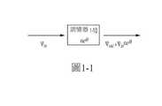
圖1-1中描繪了光學調變器(1-10)的示例,其中ψin表示輸入光場,ψout表示由調變器1-10輸出的光場,α表示振幅調變因子,θ表示相位調變因子。理想情況下,調變器1-10能夠將光場ψin的項目設置為任何相位,並結合任何衰減為ψout=αeiθ,其中α≤1且θ∈[0,2π]。因為調變器通常具有相關的Kramers-Kronig關係,和/或受到動態損失,所以簡單地設置α和θ的值不容易實現。常規地,具有兩個可獨立控制的調變信號的兩個或更多個調變器,用於以表示有號實數的方式編碼光場的振幅和相位。然而,具有多個可控制的調變信號需要複數的多變量編碼方案,通常涉及用於同時控制光學信號的相位和強度的反饋迴路。Figure 1-1 depicts an example of an optical modulator (1-10), where ψin represents the input light field, ψout represents the light field output by the modulator 1-10, α represents the amplitude modulation factor, and θ Indicates the phase modulation factor. Ideally, the modulator 1-10 can set the item of the light field ψin to any phase, combined with any attenuation as ψout =αeiθ , where α≤1 andθε [0,2π]. Because modulators usually have related Kramers-Kronig relationships and/or suffer from dynamic losses, it is not easy to simply set the values of α and θ. Conventionally, two or more modulators with two independently controllable modulation signals are used to encode the amplitude and phase of the light field in a manner that represents a signed real number. However, having multiple controllable modulation signals requires a complex multivariable encoding scheme, which usually involves a feedback loop for simultaneously controlling the phase and intensity of the optical signal.
存在能夠在不影響相位的情況下調變強度的光學調變器,包括基於電光材料的調變器。遺憾的是,電光學調變器在大規模商業環境中工作具有挑戰性,因為他們涉及使用不實用的材料來製造。There are optical modulators that can modulate the intensity without affecting the phase, including modulators based on electro-optical materials. Unfortunately, electro-optical modulators are challenging to work in large-scale commercial environments because they involve the use of impractical materials.
傳統的電腦本身不執行複數的算術運算。相反的,他們使用有號的算術,其中數字可以是正數或負數,並且可以通過執行多個計算並組合結果來建立複數的算術。發明人已經認識並理解到,即使在存在動態損耗和/或非理想相位或強度調變器的情況下,也可以利用該事實來顯著簡化有號實數線性變換的實現。Traditional computers themselves do not perform arithmetic operations on complex numbers. Instead, they use signed arithmetic, where numbers can be positive or negative, and they can build complex arithmetic by performing multiple calculations and combining the results. The inventor has recognized and understood that even in the presence of dynamic loss and/or non-ideal phase or intensity modulators, this fact can be used to significantly simplify the implementation of signed real linear transformations.
一些實施例涉及使用非理想光學調變器(其中強度調變引起相位調變且相位調變引起強度調變的調變器)來編碼有號實數的矢量的技術。與其他實施方式相反,一些這樣的實施例涉及使用單個調變信號來控制光學信號的相位以及強度。發明人已經意識到,當使用單個調變信號將有號實數編碼到光場上時,光學信號在相空間中的精確位置(例如,實部和虛部,或振幅和相位)對於解碼的目的是不重要的。根據一些實施例,對於精確解碼而言重要的是光學信號在實軸(或預先選擇作為測量軸的其他任意軸)上的投影。為了在預選軸上執行投影,在一些實施例中,使用相干偵測方案。Some embodiments involve techniques for encoding a vector of signed real numbers using a non-ideal optical modulator (a modulator in which intensity modulation causes phase modulation and phase modulation causes intensity modulation). Contrary to other embodiments, some of these embodiments involve the use of a single modulation signal to control the phase and intensity of the optical signal. The inventor has realized that when a single modulated signal is used to encode a signed real number onto a light field, the precise position of the optical signal in the phase space (for example, real and imaginary parts, or amplitude and phase) is important for decoding purposes. Is not important. According to some embodiments, what is important for accurate decoding is the projection of the optical signal on the real axis (or any other axis pre-selected as the measurement axis). In order to perform projection on a preselected axis, in some embodiments, a coherent detection scheme is used.
本文描述的類型的光域編碼技術可以用於各種環境中,包括但不限於用於短距離、中距離和長距離應用的高速電信,用於感測、通信和計算的晶片相敏測量,和使用光子處理器的光機器學習。Optical domain coding techniques of the type described herein can be used in a variety of environments, including but not limited to high-speed telecommunications for short-distance, medium-distance, and long-distance applications, wafer phase-sensitive measurement for sensing, communication, and computing, and Optical machine learning using photon processors.
更一般而言,本文描述的類型的編碼技術可以用於根據實數變換處理光學信號的任何上下文中(相對於複數變換)。傳統的電腦不直接執行複數算術。相反的,傳統電腦使用有號實數算術,其中數字可以是正數或負數。在一些實施例中,通過執行涉及實數運算的若干計算,可以在光域中建立複數運算。考慮例如光線性系統,其被配置為根據以下表達式來變換光學信號:

應當注意,基於該等式,輸入場x的實部和虛部僅貢獻於所得場y的線性獨立分量。發明人已經認識並理解到,可以通過在複平面中的任意軸上投影y,來使用相干接收器來解碼y。It should be noted that based on this equation, the real and imaginary parts of the input field x only contribute to the linear independent components of the resulting field y. The inventor has recognized and understood that a coherent receiver can be used to decode y by projecting y on any axis in the complex plane.
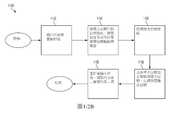
圖1-2A是根據一些實施例的實現光編碼技術的光子系統的方塊圖。光子系統1-100包括光源1-102、編碼器1-104、光學調變器1-106和光學變換單元1-108、相干接收器1-110、本地振盪器1-112和解碼器1-114。在一些實施例中,光子系統1-100可以包括圖1-2A中未示出的附加或替代組件。在一些實施例中,圖1-2A的一些或所有組件可以設置在同一半導體基板(例如,矽基板)上。Figure 1-2A is a block diagram of an optical subsystem implementing optical encoding technology according to some embodiments. The optical subsystem 1-100 includes a light source 1-102, an encoder 1-104, an optical modulator 1-106 and an optical conversion unit 1-108, a coherent receiver 1-110, a local oscillator 1-112 and a decoder 1- 114. In some embodiments, the photonic system 1-100 may include additional or alternative components not shown in FIGS. 1-2A. In some embodiments, some or all of the components of FIGS. 1-2A may be disposed on the same semiconductor substrate (for example, a silicon substrate).
光源1-102可以以多種方式實現,包括例如使用光相干源。在一個示例中,光源1-102包括配置成發射波長λ0的光的雷射。發射波長可以是電磁波譜的可見光、紅外(包括近紅外、中紅外和遠紅外)或紫外部分。在一些實施例中,λ0可以在O波段、C波段或L波段中。使用光學調變器1-106調變光源1-102發射的光。光學調變器1-106是非理想的調變器,使得相位調變引起強度調變,並且強度調變引起相位調變。在一些實施例中,相位調變可以與根據Kramers-Kronig方程式的強度調變有關。可替代地或另外地,調變器1-106可能遭受動態損耗,其中相移導致衰減。The light sources 1-102 can be implemented in a variety of ways, including, for example, the use of optical coherent sources. In one example, a light source configured to 1-102 including the emission wavelength of a laser beam of λ0. The emission wavelength can be the visible, infrared (including near-infrared, mid-infrared, and far-infrared) or ultraviolet parts of the electromagnetic spectrum. In some embodiments, λ0 may be in the O-band, C-band, or L-band. The optical modulator 1-106 is used to modulate the light emitted by the light source 1-102. The optical modulator 1-106 is a non-ideal modulator, such that phase modulation causes intensity modulation, and intensity modulation causes phase modulation. In some embodiments, phase modulation may be related to intensity modulation according to the Kramers-Kronig equation. Alternatively or additionally, the modulator 1-106 may suffer from dynamic losses, where the phase shift causes attenuation.
在一些實施例中,調變器1-106由單個電調變信號1-105驅動。因此,單個調變信號調變光場的相位和振幅。這與在光通信中常規使用的調變器形成對比,以在光場的複數振幅中編碼符號,其中每個符號代表多於一個位元。事實上,在這種類型的調變器中,多個調變信號調變光場。考慮例如配置為提供正交相移鍵控(QPSK)調變方案的光學調變器。在這些類型的調變器中,一個調變信號調變光場的實部,一個調變場調變光場的虛部。因此,在QPSK調變器中,使用兩個調變信號共同調變光場的相位和振幅。In some embodiments, the modulator 1-106 is driven by a single electrical modulation signal 1-105. Therefore, a single modulation signal modulates the phase and amplitude of the light field. This is in contrast to modulators conventionally used in optical communications to encode symbols in the complex amplitude of the light field, where each symbol represents more than one bit. In fact, in this type of modulator, multiple modulation signals modulate the light field. Consider, for example, an optical modulator configured to provide a quadrature phase shift keying (QPSK) modulation scheme. In these types of modulators, one modulating signal modulates the real part of the light field, and one modulating field modulates the imaginary part of the light field. Therefore, in the QPSK modulator, two modulation signals are used to jointly modulate the phase and amplitude of the light field.
可用於調變器1-106的調變器的示例,包括Mach Zehnder調變器、電光學調變器、環或盤調變器或其他類型的諧振調變器、電吸收調變器、Frank-Keldysh調變器、聲光學調變器、Stark效應調變器、磁光學調變器、熱光學調變器、液晶調變器、量子限制光學調變器和光子晶體調變器,以及其他可能類型的調變器。Examples of modulators that can be used in modulators 1-106 include Mach Zehnder modulators, electro-optical modulators, ring or disc modulators or other types of resonant modulators, electro-absorption modulators, Frank -Keldysh modulator, acousto-optical modulator, Stark effect modulator, magneto-optical modulator, thermo-optical modulator, liquid crystal modulator, quantum confinement optical modulator and photonic crystal modulator, and others Possible types of modulators.
編碼器1-104基於要編碼的實數生成調變信號1-105。例如,在一些實施例中,編碼器1-104可以包括將實數映射到調變信號的振幅的表。The encoder 1-104 generates the modulated signal 1-105 based on the real number to be encoded. For example, in some embodiments, the encoder 1-104 may include a table that maps real numbers to the amplitude of the modulated signal.
光學變換單元1-108可以被配置為變換所接收光場的強度和/或相位。例如,光學變換單元1-108可以包括光纖、光波導、光衰減器、光放大器(例如摻鉺光纖放大器)、分束器、光束組合器、調變器(例如電光學調變器、Franz-Keldysh調變器、諧振調變器或Mach Zehnder調變器等)、移相器(例如熱移相器或基於電漿色散效應的移相器)、光諧振器、雷射、或其任何合適的組合。在光通信的背景中,光學變換單元1-108可以包括光纖通信信道。光通信信道可以包括例如光纖,以及可選地包括光中繼器(例如摻鉺光纖放大器)。在光處理的上下文中,光學變換單元1-108可以包括光子處理單元,其示例在下面進一步詳細討論。在一些實施例中,光學變換單元1-108實現實數變換,使得變換的虛部基本上等於零。The optical conversion unit 1-108 may be configured to convert the intensity and/or phase of the received light field. For example, the optical conversion unit 1-108 may include optical fibers, optical waveguides, optical attenuators, optical amplifiers (such as erbium-doped fiber amplifiers), beam splitters, beam combiners, modulators (such as electro-optical modulators, Franz- Keldysh modulator, resonant modulator or Mach Zehnder modulator, etc.), phase shifter (such as thermal phase shifter or phase shifter based on plasma dispersion effect), optical resonator, laser, or any suitable The combination. In the context of optical communication, the optical conversion unit 1-108 may include an optical fiber communication channel. The optical communication channel may include, for example, optical fiber, and optionally an optical repeater (for example, an erbium-doped fiber amplifier). In the context of light processing, the optical transformation unit 1-108 may include a photon processing unit, examples of which are discussed in further detail below. In some embodiments, the optical transformation unit 1-108 implements real number transformation so that the imaginary part of the transformation is substantially equal to zero.
由光學變換單元1-108輸出的光場直接或間接地(例如在通過一個或多個其他光子部件之後)提供給相干接收器1-110。相干接收器1-110可以包括零差光接收器或外差光接收器。用於打擊接收信號的參考信號可以由本地振盪器1-112提供,如圖1-2A所示,或可以在通過光學變換單元1-108之後與調變光場一起提供。解碼器1-114可以被佈置為從相干接收器1-112輸出的信號中提取實數(或實數向量)。The light field output by the optical conversion unit 1-108 is provided directly or indirectly (for example, after passing through one or more other photonic components) to the coherent receiver 1-110. The coherent receiver 1-110 may include a homodyne optical receiver or a heterodyne optical receiver. The reference signal used to strike the received signal may be provided by the local oscillator 1-112, as shown in FIG. 1-2A, or may be provided with the modulated light field after passing through the optical conversion unit 1-108. The decoder 1-114 may be arranged to extract real numbers (or real number vectors) from the signal output by the coherent receiver 1-112.
圖1-2B是示出根據一些實施例的用於在光域中處理有號實數的方法的流程圖。可以使用圖1-2A的系統,或使用任何其他合適的系統,來執行方法1-150。方法1-150從步驟1-152開始,其中提供表示實數的值。在一些實施例中,可以對實數給予符號(即可以是正數或負數)。實數可以表示某個環境變量或參數,諸如物理條件(例如溫度、壓力等)、與對象相關聯的信息(例如位置、運動、速度、旋轉速率、加速度等)、與多媒體文件相關的信息(例如音頻文件的聲強度、像素顏色和/或圖像或視頻文件的強度)、與某種化學/有機元素或化合物相關的信息(例如濃度)、與金融資產相關的信息(例如某個證券的價格)、或任何其他合適類型的信息,包括從上述示例中獲得的信息。由有號實數代表的信息,可能由於各種原因而有用,包括例如訓練機器學習演算法,執行預測、資料分析、故障排除、或簡單地收集資料以供將來使用。Figures 1-2B are flowcharts illustrating a method for processing signed real numbers in the optical domain according to some embodiments. The system of Figure 1-2A, or any other suitable system, can be used to perform method 1-150. Method 1-150 starts with step 1-152, where a value representing a real number is provided. In some embodiments, real numbers can be given signs (that is, they can be positive or negative). Real numbers can represent certain environmental variables or parameters, such as physical conditions (such as temperature, pressure, etc.), information associated with objects (such as position, movement, speed, rotation rate, acceleration, etc.), and information related to multimedia files (such as The sound intensity of the audio file, the pixel color and/or the intensity of the image or video file), information related to a certain chemical/organic element or compound (such as concentration), information related to financial assets (such as the price of a security ), or any other suitable type of information, including information obtained from the above examples. Information represented by signed real numbers may be useful for various reasons, including, for example, training machine learning algorithms, performing predictions, data analysis, troubleshooting, or simply collecting data for future use.
在步驟1-154,可以將表示實數的值編碼到光場上。在一些實施例中,將值編碼到光場上,涉及基於該值調變光場的相位和強度。因此,光場的相位和振幅反映了編碼值。在一些實施例中,可以使用編碼器1-104和調變器1-106來執行步驟1-154(參見圖1-2A)。在一些這樣的實施例中,基於該值調變相位和振幅涉及用單個電調變信號驅動單個調變器。因此,單個調變信號調變光場的相位和振幅。再次參考圖1-2A,作為示例而非限制,編碼器1-104可以使用單個調變信號1-105來驅動光學調變器1-106。In step 1-154, the value representing the real number can be encoded onto the light field. In some embodiments, encoding a value onto the light field involves modulating the phase and intensity of the light field based on the value. Therefore, the phase and amplitude of the light field reflect the code value. In some embodiments, the encoder 1-104 and the modulator 1-106 may be used to perform steps 1-154 (see FIG. 1-2A). In some such embodiments, modulating the phase and amplitude based on the value involves driving a single modulator with a single electrical modulation signal. Therefore, a single modulation signal modulates the phase and amplitude of the light field. Referring again to FIG. 1-2A, as an example and not a limitation, the encoder 1-104 may use a single modulation signal 1-105 to drive the optical modulator 1-106.
應當注意,單個調變信號用於驅動調變器的事實,並不排除使用其他控制信號來控制調變器工作的環境。例如,一個或多個控制信號可用於控制調變器的溫度或調變器的某一部分的溫度。可以使用一個或多個控制信號來為調變器的操作供電。可以使用一個或多個控制信號在一定的操作狀態下偏壓調變器,例如將調變器偏壓在其線性區域中,或者設置調變器的波長以匹配光源的波長(例如圖1-2A的λ0)。It should be noted that the fact that a single modulation signal is used to drive the modulator does not exclude the use of other control signals to control the environment in which the modulator works. For example, one or more control signals may be used to control the temperature of the modulator or the temperature of a certain part of the modulator. One or more control signals can be used to power the operation of the modulator. One or more control signals can be used to bias the modulator under certain operating conditions, such as biasing the modulator in its linear region, or setting the wavelength of the modulator to match the wavelength of the light source (for example, Figure 1- Λ0 of 2A).
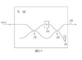
圖1-3A中示出了特定類型的調變器,根據一些實施例。調變器1-206是環形諧振調變器。應當注意,本文僅通過示例的方式描述了環形調變器,因為可以替代地使用任何其他合適類型的調變器,包括上面列出的那些。調變器1-206包括波導1-208、環1-210和移相器1-212。環1-210表現出諧振波長,其值除其他參數外還取決於環的周長。當光場ψin射入波導1-208時,光場可以或可以不耦合到環1-210,這取決於相對於環1-210的諧振波長的ψin的波長。例如,如果ψin的波長與諧振波長匹配,則ψin的至少一部分能量通過漸逝耦合傳遞到環1-210。傳遞到環的功率將在環內無限振盪,直到他完全散射或以其他方式消散。相反的,如果ψin的波長與諧振波長不匹配,則ψin可以直接通過波導1-208而沒有任何顯著的衰減。A particular type of modulator is shown in Figures 1-3A, according to some embodiments. The modulator 1-206 is a ring resonant modulator. It should be noted that the ring modulator is described herein by way of example only, as any other suitable type of modulator may be used instead, including those listed above. The modulator 1-206 includes a waveguide 1-208, a ring 1-210, and a phase shifter 1-212. The ring 1-210 exhibits a resonant wavelength, whose value depends on the circumference of the ring among other parameters. When the optical field ψin enters the waveguide 1-208, the optical field may or may not be coupled to the ring 1-210, depending on the wavelength of ψin relative to the resonance wavelength of the ring 1-210. For example, if the wavelength of ψin matches the resonance wavelength, at least a portion of the energy of ψin is transferred to the ring 1-210 through evanescent coupling. The power delivered to the ring will oscillate indefinitely within the ring until it is completely scattered or otherwise dissipated. Conversely, if the wavelength of ψin does not match the resonant wavelength, ψin can pass directly through the waveguide 1-208 without any significant attenuation.
因此,光場可以根據ψin相對於諧振波長的波長而變化。更具體地,光場的相位和強度可以根據ψin相對於諧振波長的波長而變化。圖1-3B是示出強度(頂部圖表)和相位(底部圖表)如何根據ψin相對於諧振波長的波長而變化的曲線圖。頂部圖表說明了強度光譜響應α作為ψin可能具有的所有可能波長(λ)的函數。底部圖表表示相位光譜響應θ作為相同波長的函數。在諧振頻率下,強度響應呈現下降,相位響應呈現拐點。基本上低於諧振頻率的波長,經受低強度衰減(α~1)和低相位變化(θ~0)。基本上大於諧振頻率的波長,經受低強度衰減(α~1)和符號變化(θ~-π)。在諧振波長處,ψin的強度衰減對應於下降的值,並且經受到等於拐點值的相移(即-π/2)。在圖1-3B的示例中,ψin的波長(λ0)相對於諧振頻率略微偏移。在這種情況下,ψin的強度衰減αV0(其中0>αV0>1)並且相位偏移θV0(其中-π>θV0>-π/2)。Therefore, the optical field can vary according to the wavelength of ψin with respect to the resonance wavelength. More specifically, the phase and intensity of the optical field may vary according to the wavelength of ψin with respect to the resonance wavelength. Figures 1-3B are graphs showing how intensity (top graph) and phase (bottom graph) change according to the wavelength of ψin relative to the resonance wavelength. The top graph illustrates the intensity spectral response α as a function of all possible wavelengths (λ) that ψin may have. The bottom graph shows the phase spectral response θ as a function of the same wavelength. At the resonant frequency, the intensity response shows a drop, and the phase response shows an inflection point. Wavelengths that are substantially lower than the resonance frequency experience low-intensity attenuation (α~1) and low phase changes (θ~0). Wavelengths that are substantially greater than the resonance frequency undergo low-intensity attenuation (α~1) and sign changes (θ~-π). At the resonance wavelength, the intensity attenuation of ψin corresponds to the decreasing value and undergoes a phase shift equal to the inflection point value (ie -π/2). In the example of Figure 1-3B, the wavelength of ψin (λ0 ) is slightly shifted from the resonance frequency. In this case, the intensity of ψin is attenuated by αV0 (where 0>αV0 >1) and the phase shifts by θV0 (where -π>θV0 >-π/2).
再次參考圖1-3A,可以使用電壓V來執行ψin的振幅和相位的調變,在這種情況下,電壓V體現圖1-2A的調變信號1-105。當電壓V施加到移相器1-212時,移相器的折射率改變,結果也改變了環的周長的有效長度。這反過來導致環的諧振頻率的變化。有效周長(以及相應的諧振頻率)變化的程度,取決於V的振幅。Referring again to FIGS. 1-3A, the voltage V can be used to perform the modulation of the amplitude and phase of ψin . In this case, the voltage V reflects the modulation signal 1-105 of FIG. 1-2A. When the voltage V is applied to the phase shifter 1-212, the refractive index of the phase shifter changes, and as a result, the effective length of the circumference of the ring is also changed. This in turn leads to a change in the resonance frequency of the ring. The extent to which the effective circumference (and corresponding resonant frequency) changes depends on the amplitude of V.
在圖1-3B的示例中,電壓V被設置為零。在圖1-3C的示例中,電壓設定為V1。如圖1-3C所示,將V1施加到移相器1-212導致調變器沿波長軸的強度和相位光譜響應的偏移。在這種情況下,響應呈現紅移(即向更大波長的偏移)。結果是ψin的強度現在被αV1衰減(αV1不同於αV0)並且相位偏移θV1(θV1不同於θV0)。In the example of Figures 1-3B, the voltage V is set to zero. In the example of Figure 1-3C, the voltage is set to V1 . As shown in Figure 1-3C, the application of V1 to the phase shifter 1-212 causes a shift in the intensity and phase spectral response of the modulator along the wavelength axis. In this case, the response exhibits a red shift (ie, a shift to a larger wavelength). The result is that the intensity of ψin is now attenuated by αV1 (αV1 is different from αV0 ) and the phase is shifted by θV1 (θV1 is different from θV0 ).
因此,變化的電壓V導致ψin的強度和相位的變化。換句話說,V可以被視為調變信號。在一些實施例中,電壓V可以是唯一驅動調變器1-210的調變信號。在一些實施例中,電壓V可以採用以下表達式:V=VDC+V(t),其中VDC是常數,並且V(t)隨時間變化,這取決於要編碼的實數。VDC可以預偏置環,使得諧振頻率接近ψin的波長(λ0)。Therefore, the changing voltage V causes a changein the intensity and phase of ψin . In other words, V can be regarded as a modulated signal. In some embodiments, the voltage V may be the only modulation signal that drives the modulator 1-210. In some embodiments, the voltage V may adopt the following expression: V=VDC + V(t), where VDC is a constant and V(t) varies with time, which depends on the real number to be encoded. VDC can pre-bias the ring so that the resonance frequency is close to the wavelength of ψin (λ0 ).
圖1-3D是根據一些實施例的編碼器表(例如查找表),其提供如何使用調變器1-206將實數編碼成光場的相位和強度的示例。在這種情況下,作為示例,將假設在光域中編碼具有等於1的增量的-10和10之間的實數(參見標記為「要編碼的實數」的行)。當然,可以使用本文描述的技術對任何合適的實數集進行編碼。標記為「V(施加電壓)」的行,表示施加到移相器1-212的電壓。標記為「α(振幅調變)」的行,表示在ψin的波長(λ0)處的強度光譜響應的值(參見圖1-3B和1-3C,頂部圖表)。標記為「θ(相位調變)」的行,表示在ψin的波長(λ0)處的相位光譜響應的值(參見圖1-3B和1-3C,底部圖表)。在這種情況下,實數「-10」被映射到特定電壓V1,這導致振幅調變α1和相位調變θ1;實數「-9」映射到特定電壓V2,這導致振幅調變α2和相位調變θ2;諸如此類。實數「10」被映射到特定電壓VN,這導致振幅調變αN和相位調變θN。因此,不同的實數用不同的強度/相位對編碼。Figures 1-3D are encoder tables (eg, lookup tables) according to some embodiments, which provide examples of how to use modulators 1-206 to encode real numbers into the phase and intensity of the light field. In this case, as an example, it will be assumed that a real number between -10 and 10 with an increment equal to 1 is encoded in the optical domain (see the line labeled "Real Number to Encode"). Of course, any suitable set of real numbers can be encoded using the techniques described herein. The row labeled "V (applied voltage)" represents the voltage applied to the phase shifter 1-212. The row labeled "α (amplitude modulation)" represents the value of the intensity spectral response at the wavelength of ψin (λ0 ) (see Figures 1-3B and 1-3C, top graphs). The row labeled "θ (phase modulation)" represents the value of the phase spectral response at the wavelength of ψin (λ0 ) (see Figures 1-3B and 1-3C, bottom graphs). In this case, the real number "-10" is mapped to a specific voltage V1 , which results in amplitude modulation α1 and phase modulation θ1 ; the real number "-9" is mapped to a specific voltage V2 , which results in amplitude modulation α2 and phase modulation θ2 ; and so on. The real number "10" is mapped to a specific voltage VN , which results in amplitude modulation αN and phase modulation θN. Therefore, different real numbers are encoded with different intensity/phase pairs.
圖1-3E提供了根據一些實施例的圖1-3D的編碼表的複數平面中的視覺表示。沿著線1-300的不同點,表示根據圖1-3B和圖1-3C隨著電壓變化的光譜響應的不同強度/相位對。例如,符號Sin表示以強度調變α和相位調變θ為特徵的特定符號。Sin表示圖1-3D的表中的某一列。表的每一列都映射到線1-300上的不同點。Figures 1-3E provide a visual representation in the complex plane of the coding table of Figures 1-3D according to some embodiments. The different points along the line 1-300 represent different intensity/phase pairs according to the spectral response of Figs. 1-3B and 1-3C with voltage changes. For example, the symbolSin represents a specific symbol characterized by intensity modulation α and phase modulation θ. Sin the table represents a column in FIG. 1-3D. Each column of the table is mapped to a different point on the line 1-300.
再次參考圖1-2B,在步驟1-156,對由調變器輸出的調變光學信號應用變換。變換可以涉及強度變換和/或相變,這取決於人們希望處理編碼的實數的方式。在一些實施例中,光學變換單元1-108可以用於由調變器1-106輸出的信號的變換。光學變換單元1-108可以被配置為將由強度α和相位θ表徵的符號Sin變換為符號Sout,其特徵在於強度αβ和相位θ+Δθ。換句話說,光學變換單元1-108引入強度調變β和相移Δθ。β和Δθ的值取決於所使用的特定光學變換單元。Referring again to FIG. 1-2B, in step 1-156, a transformation is applied to the modulated optical signal output by the modulator. The transformation may involve intensity transformation and/or phase transformation, depending on how one wishes to process the encoded real numbers. In some embodiments, the optical conversion unit 1-108 may be used for conversion of the signal output by the modulator 1-106. The optical transformation unit 1-108 may be configured to transform the symbol Sin represented by the intensity α and the phase θ into the symbol Sout , which is characterized by the intensity αβ and the phase θ+Δθ. In other words, the optical conversion unit 1-108 introduces intensity modulation β and phase shift Δθ. The values of β and Δθ depend on the specific optical conversion unit used.
作為示例考慮圖1-3E的輸入符號Sin,圖1-4A至1-4C提供了光學變換單元如何執行變換的示例。圖1-4A的變換使得β>1且Δθ=0。也就是說,光學變換單元引入衰減但不改變輸入光場的相位。例如,這可能是不具有光中繼器的光纖的情況,而光纖的長度被選擇為保持輸入相位。結果是,線1-300被轉換為線1-401,其中線1-401是線1-300的壓縮版本。輸出樣本Sout具有與Sin相同的相位,但強度等於αβ(即被β衰減)。As an example consider Fig. 1-3E input symbol Sin, FIGS. 1-4A to 1-4C example of how an optical transform unit performing transform. The transformation of Figure 1-4A makes β>1 and Δθ=0. That is, the optical conversion unit introduces attenuation but does not change the phase of the input light field. For example, this may be the case for an optical fiber without an optical repeater, and the length of the optical fiber is selected to maintain the input phase. The result is that line 1-300 is converted to line 1-401, where line 1-401 is a compressed version of line 1-300. Output samples Sin Sout having the same phase, but the strength is equal to alpha] [beta (β i.e. attenuation).
圖1-4B的變換引入衰減以及相移。例如,這可能是不具光中繼器的光纖,而光纖具有任意長度。結果是,線1-300被轉換為線1-402,其中線1-402是線1-300的壓縮和旋轉版本。輸出樣本Sout具有相位θ+Δθ和強度αβ。The transformation of Figure 1-4B introduces attenuation and phase shift. For example, this may be an optical fiber without an optical repeater, and the optical fiber has any length. The result is that line 1-300 is converted to line 1-402, where line 1-402 is a compressed and rotated version of line 1-300. The output sample Sout has a phase θ+Δθ and an intensity αβ.
圖1-4C的變化涉及多模態變換。當輸入光場與一個或多個其他光場組合時,這可能發生。通過多模態變換,線1-403可以以任何合適的方式重新成形。多模態變換的示例包括光處理單元,其中一些將在下面進一步詳細描述。The changes in Figure 1-4C involve multi-modal transformations. This can happen when the input light field is combined with one or more other light fields. Through multi-modal transformation, lines 1-403 can be reshaped in any suitable way. Examples of multi-modal transformations include light processing units, some of which will be described in further detail below.
再次參考圖1-2B,在步驟1-158,相干接收器可以將變換的調變光場與參考光學信號混合,以獲得電輸出信號。在一些實施例中,可以使用圖1-2A的相干接收器1-110來執行混合。參考光學信號可以是由本地振盪器(例如圖1-2A的本地振盪器1-112)生成的信號,或者可以是通過光學變換單元與調變光場一起發送的信號。混合的效果如圖1-5所示(作為示例而非限制)。線1-403(相同於圖1-4C所示的線)表示來自某個多模態變換的所有可能的強度/相位對。假設Sout是在某個時間從轉換中出來的符號。如上所述,符號Sout的特徵在於強度αβ和相位θ+Δθ。當變換場與參考信號混合時,沿著線1-403的點投影在參考軸1-500上。因此,例如,符號Sout被投影到軸1-500上的點A上。點A表示由混合產生的電輸出信號,其特徵在於振幅等於0和A(
再次參考圖1-2B,在步驟1-160,解碼器可以基於在步驟1-158獲得的電輸出信號,獲得表示解碼的實數的值。在一些實施例中,當解碼通過光變換獲得的符號時,符號在複數平面中的精確位置可能是不重要的。根據一些實施例,對於精確解碼而言重要的是光學信號在已知參考軸上的投影。換句話說,沿著線1-403的符號可以被映射到沿著參考軸的點,很像符號Sout被映射到點A。因此,一些實施例實現了光解碼方案,其中沿著參考軸的點對應於複數平面中的特定符號。Referring again to FIG. 1-2B, in step 1-160, the decoder may obtain a value representing the decoded real number based on the electrical output signal obtained in step 1-158. In some embodiments, when decoding symbols obtained by optical transformation, the precise position of the symbols in the complex plane may not be important. According to some embodiments, what is important for accurate decoding is the projection of the optical signal on a known reference axis. In other words, the symbols along the lines 1-403 can be mapped to points along the reference axis, much like the symbol Sout is mapped to point A. Therefore, some embodiments implement optical decoding schemes in which the points along the reference axis correspond to specific symbols in the complex plane.
可以使用校準過程來確定沿著參考軸的點被映射到複數平面中的符號的方式。在校準過程期間,已知強度和相位的一組輸入符號(代表一組實數的符號)通過某個光學變換單元,並且使用具有已知的參考信號來相干地偵測所得到的符號。產生的電輸出信號的振幅(即沿參考軸的投影的振幅)被記錄並存儲在表格(例如查找表)中。隨後可以在操作期間使用該表,來基於沿參考軸的投影的振幅來解碼實數。The calibration process can be used to determine how points along the reference axis are mapped to symbols in the complex plane. During the calibration process, a set of input symbols (representing a set of real numbers) of known intensity and phase passes through an optical transformation unit, and a known reference signal is used to coherently detect the resulting symbols. The amplitude of the generated electrical output signal (ie, the amplitude of the projection along the reference axis) is recorded and stored in a table (for example, a look-up table). This table can then be used during operation to decode real numbers based on the amplitude of the projection along the reference axis.
圖1-6中根據一些實施例示出了這種表的示例。該表包括用於參考信號的相位的行(「參考相位φ」)、用於沿參考軸的投影的行(「投影
在圖1-6的示例中,僅作為示例考慮了兩個參考相位(0和π/6),而不作為限制。在φ=0時,投影-1、-0.8和1分別映射到實數-9.6、0.2和8.7。在φ=π/6處,投影-0.4、0.6和0.9分別映射到實數3.1、-5和10。因此,例如,如果使用者在使用π/6的參考相位時獲得-0.4的投影,則使用者可以推斷出解碼的實數是3.1。In the example in Figures 1-6, two reference phases (0 and π/6) are considered only as an example, not as a limitation. When φ=0, projections -1, -0.8 and 1 are mapped to real numbers -9.6, 0.2 and 8.7, respectively. At φ=π/6, the projections -0.4, 0.6, and 0.9 are mapped to real numbers 3.1, -5, and 10, respectively. Therefore, for example, if the user obtains a projection of -0.4 when using a reference phase of π/6, the user can infer that the decoded real number is 3.1.
圖1-7示出了根據一些實施例的光子系統1-700的具體示例,其中光學變換單元包括光纖1-708。該示例說明如何在光通信的背景中使用本文描述的類型的編碼技術。在該實現中,光纖1-708將發射機1-701與接收器1-702分開。Figures 1-7 show specific examples of the optical subsystem 1-700 according to some embodiments, where the optical conversion unit includes an optical fiber 1-708. This example illustrates how to use encoding techniques of the type described herein in the context of optical communications. In this implementation, the fiber 1-708 separates the transmitter 1-701 from the receiver 1-702.
發射機1-701包括光源1-102、編碼器1-104和光學調變器1-106(在上面結合圖1-2A描述),接收器1-702包括相干接收器1-110和解碼器1-114(也在上面結合圖1-2A描述)。如上所述,在一些實施例中,可以使用單個調變信號1-105來驅動光學調變器1-106。在一些這樣的實施例中,光學調變器1-106可以實現開關鍵控(OOK)調變方案。The transmitter 1-701 includes a light source 1-102, an encoder 1-104 and an optical modulator 1-106 (described above in conjunction with Figure 1-2A), and the receiver 1-702 includes a coherent receiver 1-110 and a decoder 1-114 (also described above in conjunction with Figure 1-2A). As described above, in some embodiments, a single modulation signal 1-105 may be used to drive the optical modulator 1-106. In some such embodiments, the optical modulator 1-106 may implement an on-off keying (OOK) modulation scheme.
應當注意,在該實現中,用於相干偵測的參考信號直接從發射機1-701提供,而不是在接收器1-702本地生成(儘管其他實現例可能涉及接收器1-702處的本地振盪器)。為了說明這個概念,考慮例如圖1-8的曲線圖。圖1-8示出了發射機1-701的輸出處的光場的功率譜密度的示例。如圖所示,功率譜密度包括信號1-800以及載波1-801。信號1-800表示使用調變器1-106編碼的信息。載波1-801表示光源1-102波長處(λ0)的色調。在通過光纖1-708傳輸該光場時,相干接收器1-110可以使用載波1-801本身作為參考信號來執行混合。It should be noted that, in this implementation, the reference signal used for coherent detection is provided directly from the transmitter 1-701 instead of being generated locally at the receiver 1-702 (although other implementations may involve local Oscillator). To illustrate this concept, consider the graph of Figure 1-8, for example. Figures 1-8 show examples of the power spectral density of the optical field at the output of the transmitter 1-701. As shown in the figure, the power spectral density includes signal 1-800 and carrier 1-801. Signal 1-800 represents information encoded using modulator 1-106. The carrier 1-801 represents the hue at the wavelength (λ0 ) of the light source 1-102. When transmitting the light field through the optical fiber 1-708, the coherent receiver 1-110 can use the carrier 1-801 itself as a reference signal to perform mixing.
一些實施例涉及用於製造本文所述類型的光子系統的方法。圖1-9根據一些實施例描繪了一種這樣的方法。方法1-900開始於步驟1-902,其中製造調變器。可以將調變器製造成用單個電調變信號驅動。調變器的一個例子是調變器1-106(圖1-2A)。在步驟1-904,製造相干接收器。在一些實施例中,相干接收器製造在製造調變器的相同半導體基板上。在步驟1-906,製造光學變換單元。光學變換單元可以製造在製造相干接收器的同一基板上和/或製造在其上製造調變器的同一半導體基板上。可以將光學變換單元製造成耦合在調變器和相干接收器之間。光學變換單元的示例是光學變換單元1-108(圖1-2A)。II. 光學變換單元的例子Some embodiments relate to methods for manufacturing photonic systems of the type described herein. Figures 1-9 depict one such method according to some embodiments. Method 1-900 begins at step 1-902, where a modulator is manufactured. The modulator can be manufactured to be driven by a single electrical modulation signal. An example of a modulator is modulator 1-106 (Figure 1-2A). In steps 1-904, a coherent receiver is manufactured. In some embodiments, the coherent receiver is fabricated on the same semiconductor substrate where the modulator is fabricated. In steps 1-906, an optical conversion unit is manufactured. The optical conversion unit may be manufactured on the same substrate on which the coherent receiver is manufactured and/or on the same semiconductor substrate on which the modulator is manufactured. The optical conversion unit can be manufactured to be coupled between the modulator and the coherent receiver. An example of the optical conversion unit is the optical conversion unit 1-108 (Figure 1-2A).II. Examples of optical conversion units
如上所述,某些光學變換單元可以以多模態方式操作,其中多個光場被組合在一起以產生任意變換。在一些實施例中,多模態光學變換單元可以包括光子處理系統或者是光子處理系統的一部分。As mentioned above, certain optical transformation units can operate in a multi-modal manner, where multiple light fields are combined to produce arbitrary transformations. In some embodiments, the multi-modal optical conversion unit may include or be a part of a photon processing system.
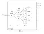
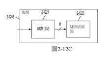
參照圖2-1,根據一些實施例,光子處理系統2-100包括光學編碼器2-101、光子處理器2-103、光接收器2-105和控制器2-107。在一些實施例中,光學變換單元1-108包括光子處理系統2-100(或其部分)。Referring to Figure 2-1, according to some embodiments, the photonic processing system 2-100 includes an optical encoder 2-101, a photonic processor 2-103, an optical receiver 2-105, and a controller 2-107. In some embodiments, the optical conversion unit 1-108 includes a photon processing system 2-100 (or part thereof).
光子處理系統2-100接收由一組輸入位元串表示的輸入向量以作為來自外部處理器(例如CPU)的輸入,並產生由一組輸出位元串表示的輸出向量。例如,如果輸入向量是n維向量,則輸入向量可以由n個單獨的位元串表示,每個位元串表示向量的相應分量。輸入位元串可以作為來自外部處理器的電信號或光學信號被接收,並且輸出位元串可以作為電信號或光學信號被發送到外部處理器。在一些實施例中,控制器2-107不必在每次處理迭代之後輸出輸出位元串。相對的,控制器2-107可以使用一個或多個輸出位元串,來確定要饋送通過光子處理系統2-100的組件的新輸入位元串流。在一些實施例中,輸出位元串本身可以用作對於由光子處理系統2-100實現的處理的後續迭代的輸入位元串。在其他實施例中,以各種方式組合多個輸出位元串流,以確定後續輸入位元串。例如,可以將一個或多個輸出位元串相加在一起,作為後續輸入位元串的確定的一部分。The photon processing system 2-100 receives an input vector represented by a set of input bit strings as input from an external processor (such as a CPU), and generates an output vector represented by a set of output bit strings. For example, if the input vector is an n-dimensional vector, the input vector can be represented by n individual bit strings, each bit string representing a corresponding component of the vector. The input bit string may be received as an electrical signal or an optical signal from the external processor, and the output bit string may be sent to the external processor as an electrical signal or optical signal. In some embodiments, the controller 2-107 need not output the output bit string after each processing iteration. In contrast, the controller 2-107 may use one or more output bit strings to determine a new input bit stream to be fed through the components of the photon processing system 2-100. In some embodiments, the output bit string itself may be used as the input bit string for subsequent iterations of the processing implemented by the photon processing system 2-100. In other embodiments, multiple output bit streams are combined in various ways to determine subsequent input bit strings. For example, one or more output bit strings can be added together as part of the determination of subsequent input bit strings.
光學編碼器2-101被配置為將輸入位元串轉換為光學編碼資訊,以由光子處理器2-103處理。在一些實施例中,每個輸入位元串由控制器2-107以電信號的形式發送到光學編碼器2-101。光學編碼器2-101將輸入向量的每個分量從其數位位元串轉換為光學信號。在一些實施例中,光學信號以光學脈衝的振幅和相位表示相關位元串的值和符號。在一些實施例中,相位可以限於零相移或π相移的二元選擇,分別表示正值和負值。實施例不限於實際輸入向量值。複數向量分量可以例如由在編碼光學信號時使用多於兩個相位值來表示。在一些實施例中,光學編碼器2-101將位元串作為來自控制器2-107的光學信號(例如數位光學信號)接收。在這些實施例中,光學編碼器2-101將數位光學信號轉換成上述類型的類比光學信號。The optical encoder 2-101 is configured to convert the input bit string into optical encoding information for processing by the photonic processor 2-103. In some embodiments, each input bit string is sent by the controller 2-107 to the optical encoder 2-101 in the form of an electrical signal. The optical encoder 2-101 converts each component of the input vector from its digital bit string into an optical signal. In some embodiments, the optical signal represents the value and sign of the relevant bit string in terms of the amplitude and phase of the optical pulse. In some embodiments, the phase may be limited to a binary choice of zero phase shift or π phase shift, representing positive and negative values, respectively. The embodiments are not limited to actual input vector values. The complex vector component can be represented, for example, by using more than two phase values when encoding the optical signal. In some embodiments, the optical encoder 2-101 receives the bit string as an optical signal (eg, a digital optical signal) from the controller 2-107. In these embodiments, the optical encoder 2-101 converts digital optical signals into analog optical signals of the type described above.
光學編碼器2-101輸出n個單獨的光學脈衝,這些光學脈衝被傳輸到光子處理器2-103。光學編碼器2-101的每個輸出,一對一地耦合到光子處理器2-103的單個輸入。在一些實施例中,光學編碼器2-101可以與光子處理器2-103設置在同一基板上(例如,光學編碼器2-101和光子處理器2-103在同一晶片上)。在這樣的實施例中,光學信號可以在波導(諸如矽光子波導)中從光學編碼器2-101傳輸到光子處理器2-103。在其他實施例中,光學編碼器2-101可以設置在與光子處理器2-103分開的基板上。在這樣的實施例中,光學信號可以在光纖中從光學編碼器2-101傳輸到光子處理器103。The optical encoder 2-101 outputs n individual optical pulses, and these optical pulses are transmitted to the photonic processor 2-103. Each output of the optical encoder 2-101 is coupled one-to-one to a single input of the photonic processor 2-103. In some embodiments, the optical encoder 2-101 and the photonic processor 2-103 may be provided on the same substrate (for example, the optical encoder 2-101 and the photonic processor 2-103 are on the same wafer). In such an embodiment, the optical signal may be transmitted from the optical encoder 2-101 to the photonic processor 2-103 in a waveguide (such as a silicon photonic waveguide). In other embodiments, the optical encoder 2-101 may be provided on a substrate separate from the photonic processor 2-103. In such an embodiment, the optical signal may be transmitted from the optical encoder 2-101 to the photonic processor 103 in an optical fiber.
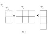
光子處理器2-103執行輸入向量乘以矩陣M。如下面詳細描述的,使用奇異值分解(SVD)和酉矩陣分解的組合,將矩陣M分解成三個矩陣。在一些實施例中,使用與QR分解中的Givens旋轉類似的運算,來執行酉矩陣分解。例如,可以使用結合Householder分解的SVD。可以由控制器2-107執行將矩陣M分解成三個組成部分,並且每個組成部分可以由光子處理器2-103的一部分實現。在一些實施例中,光子處理器2-103包括三個部分:第一可變分束器陣列(VBS),其被配置為對輸入光學脈衝陣列實現相當於第一矩陣乘法的變換(例如參見圖2-3的第一矩陣實現例2-301);一組可控光學元件,被配置為調整從第一陣列接收的每個光學脈衝的強度和/或相位,此調整相當於將第二矩陣乘以對角矩陣(參見例如圖2-3的第二矩陣實現例2-303);以及第二VBS陣列,被配置為對從可控電光元件組接收的光學脈衝實施變換,此變換相當於第三矩陣乘法(例如參見圖3的第三矩陣實現例2-305)。The photon processor 2-103 performs the multiplication of the input vector by the matrix M. As described in detail below, a combination of singular value decomposition (SVD) and unitary matrix decomposition is used to decompose matrix M into three matrices. In some embodiments, an operation similar to Givens rotation in QR decomposition is used to perform unitary matrix decomposition. For example, SVD combined with Householder decomposition can be used. The decomposition of the matrix M into three components can be performed by the controller 2-107, and each component can be realized by a part of the photon processor 2-103. In some embodiments, the photonic processor 2-103 includes three parts: a first variable beam splitter array (VBS), which is configured to implement a transformation equivalent to the first matrix multiplication on the input optical pulse array (for example, see The first matrix implementation example 2-301 of Figure 2-3); a set of controllable optical elements configured to adjust the intensity and/or phase of each optical pulse received from the first array, this adjustment is equivalent to the second The matrix is multiplied by the diagonal matrix (see, for example, the second matrix implementation example 2-303 in Figure 2-3); and the second VBS array is configured to transform the optical pulses received from the controllable electro-optical element group, which is equivalent to In the third matrix multiplication (for example, see the third matrix implementation example 2-305 in Figure 3).
光子處理器2-103輸出n個單獨的光學脈衝,這些光學脈衝被傳輸到光接收器2-105。光子處理器2-103的每個輸出,一對一地耦合到光接收器2-105的單個輸入。在一些實施例中,光子處理器2-103可以與光接收器2-105設置在同一基板上(例如,光子處理器2-103和光接收器2-105在同一晶片上)。在這樣的實施例中,光學信號可以在矽光子波導中從光子處理器2-103傳輸到光接收器2-105。在其他實施例中,光子處理器2-103可以設置在與光接收器2-105分開的基板上。在這樣的實施例中,光學信號可以在光纖中從光子處理器2-103傳輸到光接收器2-105。The photon processor 2-103 outputs n individual optical pulses, and these optical pulses are transmitted to the optical receiver 2-105. Each output of the photonic processor 2-103 is coupled one to one to a single input of the optical receiver 2-105. In some embodiments, the photonic processor 2-103 and the optical receiver 2-105 may be provided on the same substrate (for example, the photonic processor 2-103 and the optical receiver 2-105 are on the same wafer). In such an embodiment, the optical signal can be transmitted from the photonic processor 2-103 to the optical receiver 2-105 in the silicon photonic waveguide. In other embodiments, the photonic processor 2-103 may be provided on a substrate separate from the optical receiver 2-105. In such an embodiment, the optical signal may be transmitted from the photonic processor 2-103 to the optical receiver 2-105 in an optical fiber.
光接收器2-105接收來自光子處理器2-103的n個光學脈衝。然後將每個光學脈衝轉換成電信號。在一些實施例中,每個光學脈衝的強度和相位由光接收器內的光偵測器測量。然後將表示那些測量值的電信號輸出到控制器2-107。The optical receiver 2-105 receives n optical pulses from the photonic processor 2-103. Then each optical pulse is converted into an electrical signal. In some embodiments, the intensity and phase of each optical pulse are measured by a light detector in the light receiver. Then output electrical signals representing those measured values to the controller 2-107.
控制器2-107包括記憶體2-109和用於控制光學編碼器2-101、光子處理器2-103和光學接收器2-105的處理器2-111。記憶體2-109可用於存儲來自光接收器2-105的輸入和輸出位元串和測量結果。記憶體2-109還存儲可執行指令,當由處理器2-111執行時,控制光學編碼器2-101、執行矩陣分解演算法、控制光子處理器103的VBS、以及控制光學接收器2-105。記憶體2-109還可以包括可執行指令,其使得處理器2-111基於由光接收器2-105執行的測量確定的一個或多個輸出向量的集合,來確定要發送到光學編碼器的新輸入向量。以這種方式,控制器2-107可以藉由調整光子處理器2-103的設置並將來自光接收器2-105的偵測資訊反饋到光學編碼器2-101,來控制將輸入向量乘以多個矩陣的迭代過程。因此,由光子處理系統2-100發送到外部處理器的輸出向量,可以是多個矩陣乘法的結果,而不僅僅是單個矩陣乘法。The controller 2-107 includes a memory 2-109 and a processor 2-111 for controlling the optical encoder 2-101, the photonic processor 2-103, and the optical receiver 2-105. The memory 2-109 can be used to store the input and output bit strings and measurement results from the optical receiver 2-105. The memory 2-109 also stores executable instructions. When executed by the processor 2-111, it controls the optical encoder 2-101, executes the matrix decomposition algorithm, controls the VBS of the photon processor 103, and controls the optical receiver 2- 105. The memory 2-109 may also include executable instructions that cause the processor 2-111 to determine the set of one or more output vectors to be sent to the optical encoder based on the set of one or more output vectors determined by the measurement performed by the optical receiver 2-105. New input vector. In this way, the controller 2-107 can control the multiplication of the input vector by adjusting the settings of the photon processor 2-103 and feeding back the detection information from the optical receiver 2-105 to the optical encoder 2-101. Iterative process with multiple matrices. Therefore, the output vector sent by the photon processing system 2-100 to the external processor may be the result of multiple matrix multiplications, not just a single matrix multiplication.
在一些實施例中,矩陣可能太大而不能使用單次通過以在光子處理器中編碼。在這種情況下,可以在光子處理器中對大矩陣的一部分進行編碼,並且可以對大矩陣的此單個部分執行乘法處理。第一運算的結果可以存儲在記憶體2-109中。隨後,可以在光子處理器中對大矩陣的第二部分進行編碼,並且可以執行第二乘法處理。這種對大矩陣的「分塊」可以繼續,直到對大矩陣的所有部分執行乘法處理為止。然後可以組合可以存儲在記憶體2-109中的多個乘法處理的結果,以形成輸入向量乘以大矩陣的最終結果。In some embodiments, the matrix may be too large to use a single pass to encode in the photonic processor. In this case, a part of the large matrix can be encoded in the photonic processor, and the multiplication process can be performed on this single part of the large matrix. The result of the first operation can be stored in the memory 2-109. Subsequently, the second part of the large matrix can be encoded in the photonic processor, and a second multiplication process can be performed. This "blocking" of the large matrix can continue until all parts of the large matrix are multiplied. The results of multiple multiplications that can be stored in the memory 2-109 can then be combined to form the final result of multiplying the input vector by the large matrix.
在其他實施例中,外部處理器僅使用輸出向量的集合性行為。在這樣的實施例中,僅將諸如多個輸出向量的平均值或最大值/最小值的集合性結果,發送到外部處理器。III. 光學編碼器In other embodiments, the external processor only uses the collective behavior of the output vector. In such an embodiment, only aggregate results such as the average value or maximum/minimum value of a plurality of output vectors are sent to the external processor.III. Optical encoder
如圖2-2所示,根據一些實施例,光學編碼器包括至少一個光源2-201、冪次樹2-203、振幅調變器2-205、相位調變器2-207、相關聯於振幅調變器2-205的數位類比轉換器(DAC)2-209、以及相關聯於相位調變器2-207的DAC 2-211。雖然在圖2-2中將振幅調變器2-205和相位調變器2-207示為具有n個輸入和n個輸出的單個模塊(每個輸入和輸出例如是波導),在一些實施例中,每個波導可以包括相應的振幅調變器和相應的相位調變器,使得光學編碼器包括n個振幅調變器和n個相位調變器。再者,每個振幅和相位調變器可以有一個單獨的DAC。在一些實施例中,可以使用單個調變器來編碼振幅和相位資訊兩者,而不是具有與每個波導相關聯的振幅調變器和單獨的相位調變器。雖然使用單個調變器來執行這種編碼限制了精確調諧每個光學脈衝的振幅和相位的能力,但是存在不需要精確調諧光學脈衝的振幅和相位的一些編碼方案。這種方案將在後面描述。As shown in Figure 2-2, according to some embodiments, the optical encoder includes at least one light source 2-201, a power tree 2-203, an amplitude modulator 2-205, a phase modulator 2-207, The digital-to-analog converter (DAC) 2-209 of the amplitude modulator 2-205 and the DAC 2-211 associated with the phase modulator 2-207. Although the amplitude modulator 2-205 and the phase modulator 2-207 are shown as a single module with n inputs and n outputs in Fig. 2-2 (each input and output is a waveguide, for example), in some implementations In an example, each waveguide may include a corresponding amplitude modulator and a corresponding phase modulator, so that the optical encoder includes n amplitude modulators and n phase modulators. Furthermore, each amplitude and phase modulator can have a separate DAC. In some embodiments, a single modulator may be used to encode both amplitude and phase information, rather than having an amplitude modulator and a separate phase modulator associated with each waveguide. Although the use of a single modulator to perform such encoding limits the ability to precisely tune the amplitude and phase of each optical pulse, there are some encoding schemes that do not require precise tuning of the amplitude and phase of the optical pulse. This scheme will be described later.
光源2-201可以是任何合適的相干光源。在一些實施例中,光源2-201可以是二極體雷射或垂直腔表面發射雷射(VCSEL)。在一些實施例中,光源2-201被配置為具有大於10mW、大於25mW、大於50mW或大於75mW的輸出功率。在一些實施例中,光源2-201被配置為具有小於100mW的輸出功率。光源2-201可以被配置為在一個或多個波長下(例如C波段或O波段)發射連續的光波或光脈衝(「光學脈衝」)。光學脈衝的時間持續時間可以是例如大約100ps。The light source 2-201 can be any suitable coherent light source. In some embodiments, the light source 2-201 may be a diode laser or a vertical cavity surface emitting laser (VCSEL). In some embodiments, the light source 2-201 is configured to have an output power greater than 10 mW, greater than 25 mW, greater than 50 mW, or greater than 75 mW. In some embodiments, the light source 2-201 is configured to have an output power of less than 100 mW. The light source 2-201 may be configured to emit continuous light waves or light pulses ("optical pulses") at one or more wavelengths (for example, C-band or O-band). The time duration of the optical pulse may be, for example, about 100 ps.
雖然圖2-2將光源2-201示為與光學編碼器的其他部件在同一半導體基板上,但實施例不限於此。例如,光源2-201可以是單獨的雷射封裝,其邊緣粘合或表面粘合到光學編碼器晶片。或者,光源2-201可以完全在晶片外,並且光學脈衝可以經由光纖和/或光柵耦合器耦合到光學編碼器2-101的波導2-202。Although FIG. 2-2 shows the light source 2-201 as being on the same semiconductor substrate as other components of the optical encoder, the embodiment is not limited thereto. For example, the light source 2-201 may be a separate laser package with edge or surface bonded to the optical encoder chip. Alternatively, the light source 2-201 may be completely outside the wafer, and the optical pulse may be coupled to the waveguide 2-202 of the optical encoder 2-101 via an optical fiber and/or grating coupler.
光源2-201被示為兩個光源2-201a和2-201b,但是實施例不限於此。一些實施例可包括單個光源。包括多個光源201a-b(其可包括兩個以上的光源),可在其中一個光源發生故障的情況下提供冗餘。包括多個光源可以延長光子處理系統2-100的使用壽命。多個光源2-201a-b可以各自耦合到光學編碼器2-101的波導,然後在波導組合器處組合,此波導組合器被配置為將來自每個光源的光學脈衝引導到冪次樹2-203。在這樣的實施例中,在任何給定時間僅使用一個光源。The light source 2-201 is shown as two light sources 2-201a and 2-201b, but the embodiment is not limited thereto. Some embodiments may include a single light source. Including multiple light sources 201a-b (which can include more than two light sources), which can provide redundancy in the event that one of the light sources fails. Including multiple light sources can extend the life of the photon processing system 2-100. Multiple light sources 2-201a-b can each be coupled to the waveguide of the optical encoder 2-101 and then combined at the waveguide combiner, which is configured to guide the optical pulse from each light source to the
一些實施例可以同時使用兩個或更多個相同波長的鎖相光源,來增加進入光學編碼器系統的光學功率。來自兩個或更多個光源中的每一個的一小部分光(例如經由波導抽頭獲取),可以被引導到零差偵測器,可在其中測量差拍誤差(beat error)信號。差拍誤差信號可用於確定兩個光源之間可能的相位漂移。例如,差拍誤差信號可以被饋送到反饋電路,此反饋電路控制相位調變器,此相位調變器將一個光源的輸出鎖相到另一個光源的相位。鎖相可以被概括在主從方案中,其中N≥1個從光源被鎖相到單個主光源。結果是光學編碼器系統可用的總共N+1個鎖相光源。Some embodiments may use two or more phase-locked light sources of the same wavelength at the same time to increase the optical power entering the optical encoder system. A small portion of light from each of the two or more light sources (obtained via a waveguide tap, for example) can be directed to a homodyne detector, where a beat error signal can be measured. The beat error signal can be used to determine the possible phase shift between two light sources. For example, the beating error signal can be fed to a feedback circuit that controls a phase modulator that phase-locks the output of one light source to the phase of another light source. Phase locking can be summarized in a master-slave scheme, where N≥1 slave light sources are phase-locked to a single master light source. The result is a total of N+1 phase-locked light sources available to the optical encoder system.
在其他實施例中,每個單獨的光源可以與不同波長的光相關聯。使用多個波長的光允許一些實施例被多工化,使得可以使用相同的光學硬體同時執行多個計算。In other embodiments, each individual light source may be associated with light of a different wavelength. Using multiple wavelengths of light allows some embodiments to be multiplexed so that multiple calculations can be performed simultaneously using the same optical hardware.
冪次樹2-203被配置為將來自光源2-201的單個光學脈衝分成空間分離的光學脈衝陣列。因此,冪次樹2-203具有一個光學輸入和n個光學輸出。在一些實施例中,來自光源2-201的光學功率在與n個波導相關聯的n個光學模態上均勻地分開。在一些實施例中,冪次樹2-203是50:50分束器2-801的陣列,如圖2-8所示。冪次樹2-203的數量「深度」,取決於輸出端的波導數量。對於具有n個輸出模態的冪次樹,冪次樹2-203的深度為ceil(log2(n))。圖2-8的冪次樹2-203僅示出了樹深度為3(樹的每一層都標記在冪次樹2-203的底部)。每層包括2m-1個分束器,其中m是層數。因此,第一層具有單個分束器2-801a,第二層具有兩個分束器2-801b至2-801c,第三層具有四個分束器2-801d至2-801g。The power tree 2-203 is configured to divide a single optical pulse from the light source 2-201 into a spatially separated array of optical pulses. Therefore, the power tree 2-203 has one optical input and n optical outputs. In some embodiments, the optical power from the light source 2-201 is evenly divided across n optical modes associated with n waveguides. In some embodiments, the power tree 2-203 is an array of 50:50 beam splitters 2-801, as shown in Figures 2-8. The number "depth" of the power tree 2-203 depends on the number of waveguides at the output. For a power tree with n output modes, the depth of the power tree 2-203 is ceil(log2 (n)). The power tree 2-203 of Figure 2-8 only shows the tree depth of 3 (each level of the tree is marked at the bottom of the power tree 2-203). Each layer includes 2m-1 beam splitters, where m is the number of layers. Therefore, the first layer has a single beam splitter 2-801a, the second layer has two beam splitters 2-801b to 2-801c, and the third layer has four beam splitters 2-801d to 2-801g.
雖然冪次樹2-203被示為級聯分束器陣列(其可以實現為漸逝波導耦合器),但實施例不限於此,而是可使用將一個光學脈衝轉換為複數個空間分離的光學脈衝的任何光學設備。例如,可以使用一個或多個多模干涉儀(MMI)來實現冪次樹2-203,在這種情況下,將適當地修改管理層寬度和深度的方程式。Although the power tree 2-203 is shown as a cascaded beam splitter array (which can be implemented as an evanescent waveguide coupler), the embodiment is not limited to this, but can be used to convert one optical pulse into a plurality of spatially separated Any optical device for optical pulses. For example, one or more multimode interferometers (MMI) can be used to implement the power tree 2-203, in which case the equations for the width and depth of the management layer will be modified appropriately.
無論使用何種類型的冪次樹2-203,製造冪次樹2-203使得在n個輸出模態之間的分束比精確均勻,即使可能也會是困難的。因此,可以對振幅調變器的設置進行調整,以校正冪次樹輸出的n個光學脈衝的不等強度。例如,具有最低光學功率的波導,可以被對於傳輸到光子處理器2-103的任何給定脈衝設置為最大功率。因此,除了對用於將資訊編碼到光學脈衝中的振幅的調變之外,可以藉由振幅調變器2-205調變具有高於最大功率的功率的任何光學脈衝為具有較低的功率。相位調變器也可以放置在n個輸出模態中的每一個處,其可以用於調整冪次樹2-203的每個輸出模態的相位,使得所有輸出信號具有相同的相位。No matter what type of power tree 2-203 is used, it is difficult, if not impossible, to make the power tree 2-203 so that the splitting ratio between n output modes is precisely uniform. Therefore, the settings of the amplitude modulator can be adjusted to correct the unequal intensities of the n optical pulses output by the power tree. For example, the waveguide with the lowest optical power can be set to the maximum power for any given pulse transmitted to the photonic processor 2-103. Therefore, in addition to the modulation of the amplitude used to encode information into the optical pulse, any optical pulse with a power higher than the maximum power can be modulated by the amplitude modulator 2-205 to have a lower power . The phase modulator can also be placed at each of the n output modes, which can be used to adjust the phase of each output mode of the power tree 2-203 so that all output signals have the same phase.
可選地或另外地,可以使用一個或多個Mach-Zehnder干涉儀(MZI)來實現冪次樹2-203,MZI可以被調諧使得冪次樹中每個分束器的分束比,在冪次樹2-203的輸出處產生實質相等的強度脈衝。Alternatively or additionally, one or more Mach-Zehnder interferometers (MZI) can be used to implement the power tree 2-203. The MZI can be tuned so that the splitting ratio of each beam splitter in the power tree is The output of the power tree 2-203 produces substantially equal intensity pulses.
振幅調變器2-205被配置為基於相應的輸入位元串,修改從冪次樹2-203接收的每個光學脈衝的振幅。振幅調變器2-205可以是可變衰減器或由DAC 2-209控制的任何其他合適的振幅調變器,DAC 2-209可以進一步由控制器2-107控制。一些振幅調變器對於電信應用是已知的,並且可以在一些實施例中使用。在一些實施例中,可變分束器可以用作振幅調變器2-205,其中僅保留可變分束器的一個輸出而丟棄或忽略另一個輸出。可以在一些實施例中使用的振幅調變器的其他示例,包括行進波調變器、基於腔的調變器、Franz-Keldysh調變器、基於電漿的調變器、基於2D材料的調變器、和奈米光電機械開關(NOEMS)。The amplitude modulator 2-205 is configured to modify the amplitude of each optical pulse received from the power tree 2-203 based on the corresponding input bit string. The amplitude modulator 2-205 may be a variable attenuator or any other suitable amplitude modulator controlled by the DAC 2-209, and the DAC 2-209 may be further controlled by the controller 2-107. Some amplitude modulators are known for telecommunications applications and can be used in some embodiments. In some embodiments, the variable beam splitter can be used as the amplitude modulator 2-205, where only one output of the variable beam splitter is retained and the other output is discarded or ignored. Other examples of amplitude modulators that can be used in some embodiments include traveling wave modulators, cavity-based modulators, Franz-Keldysh modulators, plasma-based modulators, 2D material-based modulators Inverter, and Nano Photoelectric Mechanical Switch (NOEMS).
相位調變器2-207被配置為基於相應的輸入位元串,修改從冪次樹2-203接收的每個光學脈衝的相位。相位調變器可以是熱光移相器或可以由2-211電性控制的任何其他合適的移相器,2-211可以進一步由控制器2-107控制。The phase modulator 2-207 is configured to modify the phase of each optical pulse received from the power tree 2-203 based on the corresponding input bit string. The phase modulator may be a thermo-optical phase shifter or any other suitable phase shifter that can be electrically controlled by 2-211, and 2-211 may be further controlled by a controller 2-107.
雖然圖2-2示出了振幅調變器2-205和相位調變器2-207作為兩個單獨的組件,但他們可以組合成控制光學脈衝的振幅和相位兩者的單個元件。然而,分別控制光學脈衝的振幅和相位是有利的。亦即,由於經由Kramers-Kronenig關係的振幅偏移和相移之間的連結,存在與任何振幅偏移相關聯的相移。為了精確地控制光學脈衝的相位,應該使用相位調變器2-207補償由振幅調變器2-205產生的相移。舉例來說,離開光學編碼器2-101的光學脈衝的總振幅是A = a0a1a2,並且離開光學編碼器的光學脈衝的總相位是θ=Δθ+Δφ+φ,其中a0是輸入光學脈衝的輸入強度(假設調變器輸入端為零相位),a1是振幅調變器2-205的振幅衰減,Δθ是振幅調變器2-205在調變振幅時賦予的相移,Δφ是由相位調變器2-207賦予的相移,a2是與通過相位調變器2-209的光學脈衝相關的衰減,φ是由於光學信號傳播而賦予到光學信號上的相位。因此,設置光學脈衝的振幅和相位,不是兩個獨立的確定過程。相反的,為了將特定振幅和相位精確地編碼進從光學編碼器2-101輸出的光學脈衝,對於兩種設置都應考慮振幅調變器2-205和相位調變器2-207的設置。Although Figure 2-2 shows the amplitude modulator 2-205 and the phase modulator 2-207 as two separate components, they can be combined into a single element that controls both the amplitude and phase of the optical pulse. However, it is advantageous to control the amplitude and phase of the optical pulse separately. That is, due to the link between the amplitude shift and the phase shift via the Kramers-Kronenig relationship, there is a phase shift associated with any amplitude shift. In order to precisely control the phase of the optical pulse, the phase modulator 2-207 should be used to compensate the phase shift generated by the amplitude modulator 2-205. For example, the total amplitude of the optical pulse leaving the optical encoder 2-101 is A = a0 a1 a2 , and the total phase of the optical pulse leaving the optical encoder is θ=Δθ+Δφ+φ, where a0 Is the input intensity of the input optical pulse (assuming zero phase at the input of the modulator), a1 is the amplitude attenuation of the amplitude modulator 2-205, and Δθ is the phase given by the amplitude modulator 2-205 when modulating the amplitude. Δφ is the phase shift imparted by the phase modulator 2-207, a2 is the attenuation associated with the optical pulse passing through the phase modulator 2-209, and φ is the phase imparted to the optical signal due to the propagation of the optical signal . Therefore, setting the amplitude and phase of the optical pulse is not two independent determination processes. On the contrary, in order to accurately encode a specific amplitude and phase into the optical pulse output from the optical encoder 2-101, the settings of the amplitude modulator 2-205 and the phase modulator 2-207 should be considered for both settings.
在一些實施例中,光學脈衝的振幅與位元串值直接相關。例如,高振幅脈衝對應於高位元串值,而低振幅脈衝對應於低位元串值。光學脈衝的相位,將位元串值編碼為正或負。在一些實施例中,光學編碼器2-101輸出的光學脈衝的相位,可以選自相隔180度(π弧度)的兩個相位。例如,正位元串值可以用零度相移來編碼,而負位串值可以用180度(π弧度)相移來編碼。在一些實施例中,向量意為複數值,因此光學脈衝的相位選自不僅僅是0和2π之間的兩個值。In some embodiments, the amplitude of the optical pulse is directly related to the bit string value. For example, a high amplitude pulse corresponds to a high bit string value, and a low amplitude pulse corresponds to a low bit string value. The phase of the optical pulse encodes the bit string value as positive or negative. In some embodiments, the phase of the optical pulse output by the optical encoder 2-101 may be selected from two phases separated by 180 degrees (π radians). For example, a positive bit string value can be encoded with a zero degree phase shift, and a negative bit string value can be encoded with a 180 degree (π radians) phase shift. In some embodiments, the vector means a complex value, so the phase of the optical pulse is selected from more than just two values between 0 and 2π.
在一些實施例中,控制器2-107基於輸入位元串和前述將輸出振幅和輸出相位鏈接到由振幅調變器2-204和相位調變器2-207施加的振幅和相位的等式,來確定由振幅調變器2-205和相位調變器2-207兩者施加的振幅和相位。在一些實施例中,控制器2-107可以在記憶體2-109中存儲用於驅動振幅調變器2-205和相位調變器2-207的數位值表。在一些實施例中,可以將記憶體放置在調變器附近以減少通信時間性潛時和功耗。In some embodiments, the controller 2-107 is based on the input bit string and the aforementioned equation linking the output amplitude and output phase to the amplitude and phase applied by the amplitude modulator 2-204 and the phase modulator 2-207 , To determine the amplitude and phase applied by both the amplitude modulator 2-205 and the phase modulator 2-207. In some embodiments, the controller 2-107 may store a digital value table for driving the amplitude modulator 2-205 and the phase modulator 2-207 in the memory 2-109. In some embodiments, the memory can be placed near the modulator to reduce communication latency and power consumption.
與振幅調變器2-205相關聯並通信地耦合到振幅調變器2-205的數位類比轉換器(DAC)2-209,從控制器2-107接收數位驅動值,並將數位驅動值轉換為驅動振幅調變器2-205的類比電壓。類似的,與相位調變器2-207相關聯並通信地耦合到相位調變器2-207的數位類比轉換器(DAC)2-211,從控制器2-107接收數位驅動值,並將數位驅動值轉換為驅動相位調變器2-207的類比電壓。在一些實施例中,DAC可以包括放大器,放大器將類比電壓放大到足夠高的位準,以在振幅調變器內實現期望的消光比(例如,實際上可能使用特定相位調變器實現的最高消光比)並在相位調變器內實現期望的相移範圍(例如,覆蓋0到2π之間的整個範圍的相移範圍)。雖然如圖2-2所示DAC 2-209和DAC 2-211位於光學編碼器2-101的晶片中和/或晶片上,在一些實施例中,DAC 2-209和2-211可以位於晶片外,同時仍然由導電跡線和/或導線分別通信耦合到振幅調變器2-205和相位調變器2-207。A digital analog converter (DAC) 2-209 associated with the amplitude modulator 2-205 and communicatively coupled to the amplitude modulator 2-205 receives the digital drive value from the controller 2-107 and transfers the digital drive value Converted to analog voltage for driving amplitude modulator 2-205. Similarly, the digital-to-analog converter (DAC) 2-211 associated with the phase modulator 2-207 and communicatively coupled to the phase modulator 2-207 receives the digital drive value from the controller 2-107 and transfers The digital drive value is converted into an analog voltage for driving the phase modulator 2-207. In some embodiments, the DAC may include an amplifier that amplifies the analog voltage to a high enough level to achieve the desired extinction ratio in the amplitude modulator (for example, the highest possible extinction ratio may actually be achieved using a specific phase modulator) Extinction ratio) and achieve the desired phase shift range in the phase modulator (for example, covering the entire range of phase shift range between 0 and 2π). Although DAC 2-209 and DAC 2-211 are located in and/or on the die of the optical encoder 2-101 as shown in Figure 2-2, in some embodiments, DAC 2-209 and 2-211 may be located on the die In addition, while still being communicatively coupled to the amplitude modulator 2-205 and the phase modulator 2-207 by conductive traces and/or wires, respectively.
在由振幅調變器2-205和相位調變器2-207調變之後,n個光學脈衝從光學編碼器2-101傳輸到光子處理器2-103。IV. 光子處理器After being modulated by the amplitude modulator 2-205 and the phase modulator 2-207, n optical pulses are transmitted from the optical encoder 2-101 to the photonic processor 2-103.IV. Photon Processor
參考圖2-3所示,光子處理器2-103對由n輸入光學脈衝表示的輸入向量實現矩陣乘法,並包括三個主要部分:第一矩陣實現例2-301、第二矩陣實現例2-303和第三矩陣實現例2-305。在一些實施例中,如下面更詳細討論的,第一矩陣實現例2-301和第三矩陣實現例2-305包括可編程、可重新配置的可變分束器(VBS)的互連陣列,其被配置為將來自輸入向量的n個輸入光學脈衝變換為輸出向量,向量的分量由每個光學脈衝的振幅和相位表示。在一些實施例中,第二矩陣實現例2-303包括一組電光元件。As shown in Figure 2-3, the photon processor 2-103 implements matrix multiplication on the input vector represented by n input optical pulses, and includes three main parts: the first matrix implementation example 2-301, the second matrix implementation example 2 -303 and the third matrix implementation example 2-305. In some embodiments, as discussed in more detail below, the first matrix implementation example 2-301 and the third matrix implementation example 2-305 include interconnected arrays of programmable, reconfigurable variable beam splitters (VBS) , Which is configured to transform n input optical pulses from the input vector into an output vector, the components of the vector are represented by the amplitude and phase of each optical pulse. In some embodiments, the second matrix implementation example 2-303 includes a set of electro-optical elements.
輸入向量藉由使輸入光學脈衝通過光子處理器2-103而所乘以的矩陣稱為M。矩陣M是控制器2-107已知應由光子處理器2-103實現的矩陣的一般mxn。這樣,控制器2-107使用奇異值分解(SVD)分解矩陣M,使得矩陣M由三個組成矩陣表示:M =VTΣU,其中U和V分別是實正交nxn和mxm矩陣(UTU=UUT=I且VTV=VVT=I),並且Σ是具有實條目的m×n對角矩陣。所有方程式中的上標「T」表示相關矩陣的轉置。矩陣的SVD確定程序是已知的,並且控制器2-107可以使用任何合適的技術來確定矩陣M的SVD。在一些實施例中,矩陣M是複矩陣,在這種情況下矩陣M可以被分解成M=V†ΣU,其中V和U是複數酉n×n和m×m矩陣,分別是U†U=UU†=I和V†V=VV†=I),Σ是具有實數條目或複數條目的m×n對角矩陣。對角奇異值的值也可以進一步歸一化,使得奇異值的最大絕對值是1。The matrix to which the input vector is multiplied by passing the input optical pulse through the photon processor 2-103 is calledM. The matrixM is the generalm xn of the matrix known by the controller 2-107 to be implemented by the photon processor 2-103. In this way, the controller 2-107 uses singular value decomposition (SVD) to decompose the matrixM so that the matrixM is represented by three constituent matrices: M = VT ΣU, whereU andV are real orthogonaln xn andm xm, respectively Matrix (UT U =UUT =I andVT V =VVT =I ), andΣ is anm ×n diagonal matrix with real entries. The superscript "T" in all equations represents the transpose of the correlation matrix. The SVD determination procedure of the matrix is known, and the controller 2-107 can use any suitable technique to determine the SVD of the matrixM. In some embodiments, the matrix M is a complex matrix. In this case, the matrixM can be decomposed intoM =V†ΣU , whereV andU are complex unitaryn ×n andm ×m matrices, respectivelyU†U =UU† =I andV†V =VV† =I ),Σ is anm ×n diagonal matrix with real or complex entries. The value of the diagonal singular value can also be further normalized so that the maximum absolute value of the singular value is 1.
一旦控制器2-107在矩陣U和V是正交實矩陣的情況下對矩陣M確定了矩陣U、Σ和V,則控制器可以進一步將兩個正交矩陣U和V分解為一系列實數Givens旋轉矩陣。Givens旋轉矩陣G(i,j,θ)由以下方程式按分量定義:


用於以複數空間中的Givens旋轉組的乘積表達任意實正交矩陣的演算法,提供在M. Reck等人所著的「Experimental realization of any discrete unitary operator,」 Physical Review Letters 73, 58 (1994) (「Reck」),與 W. R. Clements等人所著的,「Optimal design for universal multiport interferometers,」 Optica 3, 12 (2016) (「Clements」),這兩篇文獻的全部內容通過引用併入本文,至少針對他們對根據Givens旋轉分解實正交矩陣的技術的討論。(如果本文使用的任何術語與Reck和/或Clements中該術語的使用相衝突,則術語應該被賦予與具有通常知識者如何理解其在本文中的使用最相符的含義)。得到的分解由下式給出:


作為示例而非限制,4×4正交矩陣的分解可表示為:
下面簡要概述根據可以使用控制器2-107實現的n組實值Givens旋轉來分解n×n矩陣U的演算法的一個實施例:
上述演算法的結果矩陣U'是下三角形,並且通過以下等式與原始矩陣U相關:
演算法的下一步,是重複找到使用以下演算法完成的步驟,演算法可以使用控制器2-107實現:
上述演算法也可用於分解V和/或VT,以確定m層的VBS值和相關的相位屏幕。The above algorithm can also be used to decomposeV and/orVT to determine the VBS value of them layer and the related phase screen.
將正交矩陣分解為實值Givens旋轉矩陣的上述概念可以擴展到複數矩陣,例如酉矩陣,而不是正交矩陣。在一些實施例中,這可以通過在Givens旋轉矩陣的參數化中包括附加相位來實現。因此,附加額外相位項的Givens矩陣的一般形式是T(i,j,θ,ϕ),其中


基於上述將任意酉矩陣分解為限制的Givens旋轉組的程序,可以通過特定的旋轉和相移序列來實現任何酉矩陣。並且在光子學中,旋轉可以由可變分束器(VBS)表示,並且可以使用相位調變器輕易實現相移。因此,對於光子處理器2-103的n個光學輸入,表示矩陣M的SVD的酉矩陣的第一矩陣實現例2-301和第三矩陣實現例2-305,可以由互連的VBS和移相器陣列實現。由於通過VBS陣列傳遞光學脈衝的並行性質,可以在O(1)時間內執行矩陣乘法。第二矩陣實現例2-303是矩陣M的SVD的對角矩陣,其與對應於SVD的每個正交矩陣的對角矩陣D組合。如上所述,每個矩陣D被稱為「相位屏幕」,並且可以用下標標記,以表示他是與矩陣U還是矩陣V相關聯的相位屏幕。因此,第二矩陣實現例303是矩陣Σ'=DVΣDU。Based on the above procedure of decomposing any unitary matrix into a restricted Givens rotation group, any unitary matrix can be realized through a specific rotation and phase shift sequence. And in photonics, the rotation can be represented by a variable beam splitter (VBS), and the phase shift can be easily achieved using a phase modulator. Therefore, for then optical inputs of the photon processor 2-103, the first matrix implementation example 2-301 and the third matrix implementation example 2-305 of the unitary matrix representing the SVD of matrixM can be determined by the interconnected VBS and shift Phaser array implementation. Due to the parallel nature of transmitting optical pulses through the VBS array, matrix multiplication can be performed in O(1) time. The second matrix implementation example 2-303 is the diagonal matrix of the SVD of the matrixM , which is combined with the diagonal matrixD of each orthogonal matrix corresponding to the SVD. As mentioned above, each matrix D is called a "phase screen" and can be marked with a subscript to indicate whether it is a phase screen associated with matrixU or matrixV. Therefore, the second matrix implementation example 303 is the matrix Σ'=DV ΣDU.
在一些實施例中,與第一矩陣實現例2-301和第三矩陣實現例2-305相關聯的光子處理器2-103的VBS單元,可以是具有內部移相器的Mach-Zehnder干涉儀(MZI)。在其他實施例中,VBS單元電池可以是微機電系統(MEMS)致動器。在一些實施例中,可以使用外部移相器來實現Givens旋轉所需的附加相位。In some embodiments, the VBS unit of the photon processor 2-103 associated with the first matrix implementation example 2-301 and the third matrix implementation example 2-305 may be a Mach-Zehnder interferometer with an internal phase shifter (MZI). In other embodiments, the VBS unit cell may be a microelectromechanical system (MEMS) actuator. In some embodiments, an external phase shifter can be used to achieve the additional phase required for Givens rotation.
表示對角矩陣DVΣDU的第二矩陣實現例2-303,可以使用振幅調變器和移相器來實現。在一些實施例中,VBS可用於分離可被丟棄的光的一部分以可變地衰減光學脈衝。附加地或替代地,可使用可控制式增益介質來放大光學信號。例如,GaAs、InGaAs、GaN或InP可以用作用於放大光學信號的主動增益介質。也可以使用其他主動增益處理,例如具有晶體反轉對稱的材料(例如KTP和鈮酸鋰)中的二次諧波產生,以及缺乏反轉對稱性的材料(例如矽)中的四波混合處理。取決於所實現的相位屏幕,每種光學模態中的移相器可用於施加零或π相移。在一些實施例中,對於每個相位屏幕,僅使用用於每個光學模態的單個移相器而不是一個移相器。這是可能的,因為每個矩陣DV、Σ和DU都是對角的,因此是可交換的(commute)。因此,光子處理器2-103的第二矩陣實現例2-303的每個移相器的值,是兩個相位屏幕的乘積的結果:DVDU。The second matrix implementation example 2-303 representing the diagonal matrix DV ΣDU can be implemented using an amplitude modulator and a phase shifter. In some embodiments, VBS can be used to separate a portion of light that can be discarded to variably attenuate optical pulses. Additionally or alternatively, a controllable gain medium may be used to amplify the optical signal. For example, GaAs, InGaAs, GaN, or InP can be used as an active gain medium for amplifying optical signals. Other active gain processing can also be used, such as second harmonic generation in materials with crystal inversion symmetry (such as KTP and lithium niobate), and four-wave mixing processing in materials lacking inversion symmetry (such as silicon) . Depending on the phase screen implemented, the phase shifter in each optical mode can be used to apply a zero or π phase shift. In some embodiments, for each phase screen, only a single phase shifter for each optical mode is used instead of one phase shifter. This is possible because each matrix DV , Σ, and DU is diagonal and therefore commutative. Therefore, the second matrix of the photon processor 2-103 realizes the value of each phase shifter in Example 2-303, which is the result of the product of the two phase screens: DV DU.
參考圖2-4,根據一些實施例,第一和第三矩陣實現例2-301和2-305被實現為VBS 2-401的陣列。為簡單起見,僅示出了n = 6個輸入光學脈衝(列數),導致「電路深度」(例如行數)等於輸入光學脈衝的數量(例如六個)。為清楚起見,只對一個VBS 2-401標有元件符號。然而,VBS被標記有下標與上標,下標識別特定VBS正在混合哪些光學模態,上標標記相關的行。如上所述,每個VBS 2-401實現複數Givens旋轉,T(i,j,θ,ϕ),其中i和j等效於VBS 2-401的下標標籤,θ是Givens旋轉的旋轉角度,φ是與廣義旋轉相關的附加相位。Referring to FIGS. 2-4, according to some embodiments, the first and third matrix implementation examples 2-301 and 2-305 are implemented as arrays of VBS 2-401. For simplicity, only n = 6 input optical pulses (number of columns) are shown, resulting in "circuit depth" (for example, number of rows) equal to the number of input optical pulses (for example, six). For clarity, only one VBS 2-401 is marked with component symbols. However, the VBS is marked with a subscript and a superscript. The subscript identifies which optical modalities a particular VBS is mixing, and the superscript marks the relevant line. As mentioned above, each VBS 2-401 realizes complex Givens rotation, T(i,j,θ,ϕ), where i and j are equivalent to the subscript labels of VBS 2-401, and θ is the rotation angle of Givens rotation, φ is the additional phase associated with generalized rotation.
參考圖2-5所示,每個VBS 2-401可以使用MZI 2-510和至少一個外部移相器2-507來實現。在一些實施例中,還可以包括第二外部移相器2-509。MZI 2-510包括第一瞬逝耦合器2-501和第二瞬逝耦合器2-503,用於混合MZI 2-510的兩個輸入模態。內部移相器2-505調變MZI 2-510的一個臂中的相位θ,以在兩個臂之間產生相位差。調整相位θ使得VBS 2-401的光輸出強度從MZI 2-510的一種輸出模態變化到另一種輸出模態,從而產生可控且可變的分束器。在一些實施例中,可以在第二臂上施加第二內部移相器。在這種情況下,兩個內部移相器之間的差異導致輸出光強度變化。兩個內部相位之間的平均值,將為進入模態i和模態j的光賦予全局相位。因此,兩個參數θ和φ可以各自由移相器控制。在一些實施例中,第二外部移相器2-509可用於校正由於靜態相位無序而在VBS的輸出模態上的不想要的差分相位。As shown in Figure 2-5, each VBS 2-401 can be implemented using MZI 2-510 and at least one external phase shifter 2-507. In some embodiments, a second external phase shifter 2-509 may also be included. The MZI 2-510 includes a first evanescent coupler 2-501 and a second evanescent coupler 2-503 for mixing the two input modes of the MZI 2-510. The internal phase shifter 2-505 modulates the phase θ in one arm of the MZI 2-510 to generate a phase difference between the two arms. Adjusting the phase θ makes the light output intensity of the VBS 2-401 change from one output mode of the MZI 2-510 to another output mode, thereby producing a controllable and variable beam splitter. In some embodiments, a second internal phase shifter may be applied on the second arm. In this case, the difference between the two internal phase shifters causes the output light intensity to change. The average value between the two internal phases will give a global phase to the light entering mode i and mode j. Therefore, the two parameters θ and φ can each be controlled by a phase shifter. In some embodiments, the second external phase shifter 2-509 can be used to correct the unwanted differential phase in the output mode of the VBS due to the static phase disorder.
在一些實施例中,移相器2-505、2-507和2-509可包括熱光、電光或光機械相位調變器。在其他實施例中,可以使用NOEMS調變器,而不是在MZI 510內包括內部相位調變器505。In some embodiments, the phase shifters 2-505, 2-507, and 2-509 may include thermo-optical, electro-optical, or opto-mechanical phase modulators. In other embodiments, a NOEMS modulator can be used instead of including the internal phase modulator 505 in the MZI 510.
在一些實施例中,VBS的數量隨著矩陣的大小而增長。發明人已經認識並理解到,控制大量VBS可能是具有挑戰性的,並且在多個VBS之間共享單個控制電路是有益的。可用於控制多個VBS的並行控制電路的示例,是數位類比轉換器接收數位串作為輸入,此數位串對要在特定VBS上賦予的類比信號進行編碼。在一些實施例中,電路還接收第二輸入,即要控制的VBS的位址。然後,電路可以在定址的VBS上賦予類比信號。在其他實施例中,控制電路可以自動掃描多個VBS並在多個VBS上賦予類比信號,而不被主動給予位址。在這種情況下,定址序列是預定義的,使得他以已知的順序遍歷VBS陣列。In some embodiments, the number of VBS increases with the size of the matrix. The inventor has recognized and understood that controlling a large number of VBSs can be challenging, and sharing a single control circuit among multiple VBSs is beneficial. An example of a parallel control circuit that can be used to control multiple VBSs is a digital-to-analog converter that receives a digital string as input, and this digital string encodes the analog signal to be assigned to a specific VBS. In some embodiments, the circuit also receives a second input, that is, the address of the VBS to be controlled. The circuit can then assign analog signals on the addressed VBS. In other embodiments, the control circuit can automatically scan multiple VBSs and assign analog signals to the multiple VBSs without being actively assigned addresses. In this case, the addressing sequence is predefined so that it traverses the VBS array in a known order.
參考圖2-6所示,第二矩陣實現例2-303實現了對角矩陣Σ'=DVΣDU的乘法。這可以使用兩個移相器2-601和2-605來實現兩個相位屏幕和振幅調變器2-603,以將相關光學脈衝的強度調整量η來實現。如上所述,在一些實施例中,可以僅使用單個相位調變器2-601,因為兩個相位屏幕可以組合在一起,因為形成Σ'的三個組成矩陣是對角的並且因此是可交換的。Referring to Figure 2-6, the second matrix implementation example 2-303 realizes the multiplication of the diagonal matrix Σ'=DV ΣDU. This can be achieved by using two phase shifters 2-601 and 2-605 to implement two phase screens and an amplitude modulator 2-603 to adjust the intensity of the relevant optical pulse by the amount η. As mentioned above, in some embodiments, only a single phase modulator 2-601 can be used, because two phase screens can be combined together because the three constituent matrices forming Σ'are diagonal and therefore interchangeable of.
在一些實施例中,振幅調變器2-603可以使用衰減器和/或放大器來實現。如果振幅調變η的值大於1,則光學脈衝被放大。如果振幅調變η的值小於1,則光學脈衝被衰減。在一些實施例中,僅使用衰減。在一些實施例中,衰減可以由一行集成衰減器實現。在其他實施例中,如圖2-7所示,衰減2-603可以使用包括兩個瞬逝耦合器2-701和2-703的MZI以及可控內部移相器2-705來實現,以調整從MZI輸入端傳送多少輸入光到MZI的第一輸出端口2-709。MZI的第二輸出端口2-707可以被忽略、阻止或丟棄。In some embodiments, the amplitude modulator 2-603 may be implemented using an attenuator and/or amplifier. If the value of amplitude modulation η is greater than 1, the optical pulse is amplified. If the value of amplitude modulation η is less than 1, the optical pulse is attenuated. In some embodiments, only attenuation is used. In some embodiments, attenuation can be achieved by a row of integrated attenuators. In other embodiments, as shown in Figure 2-7, the attenuation 2-603 can be realized by using an MZI including two evanescent couplers 2-701 and 2-703 and a controllable internal phase shifter 2-705 to Adjust how much input light is transmitted from the MZI input port to the first output port 2-709 of the MZI. The second output port 2-707 of MZI can be ignored, blocked or discarded.
在一些實施例中,控制器2-107控制光子處理器2-103中的每個移相器的值。上面討論的每個移相器,可以包括類似於結合光學編碼器2-101的相位調變器2-207討論的DAC的DAC。In some embodiments, the controller 2-107 controls the value of each phase shifter in the photonic processor 2-103. Each of the phase shifters discussed above may include a DAC similar to the DAC discussed in conjunction with the phase modulator 2-207 of the optical encoder 2-101.
光子處理器2-103可以包括任何數量的輸入節點,但是互連的VBS陣列2-301和2-305的尺寸和複雜性,將隨著輸入模態的數量的增加而增加。例如,如果存在n個輸入光學模態,則光子處理器2-103將具有2n + 1的電路深度,其中第一矩陣實現例2-301和第二矩陣實現例2-305各自具有電路深度n,且第二矩陣實現例2-303的電路深度為1。重要的是,執行單個矩陣乘法的時間複雜度與輸入光脈衝的數量甚至不是線性關係 - 他總為O(1)。在一些實施例中,由並行化提供的這種低階複雜性,導致使用傳統電處理器無法獲得的能量和時間效率。The photonic processor 2-103 may include any number of input nodes, but the size and complexity of the interconnected VBS arrays 2-301 and 2-305 will increase as the number of input modalities increases. For example, if there are n input optical modes, the photonic processor 2-103 will have a circuit depth of 2n + 1, where the first matrix implementation example 2-301 and the second matrix implementation example 2-305 each have a circuit depth n , And the circuit depth of the second matrix implementation example 2-303 is 1. The important thing is that the time complexity of performing a single matrix multiplication is not even linear with the number of input light pulses-it is always O(1). In some embodiments, this low-level complexity provided by parallelization results in energy and time efficiencies that cannot be obtained using traditional electrical processors.
應注意,雖然本文描述的實施例將光子處理器2-103示出為具有n個輸入和n個輸出,但是在一些實施例中,由光子處理器2-103實現的矩陣M可以不是方形矩陣。在這樣的實施例中,光子處理器2-103可以具有不同數量的輸出和輸入。It should be noted that although the embodiments described herein show the photon processor 2-103 as having n inputs and n outputs, in some embodiments, the matrix M implemented by the photon processor 2-103 may not be a square matrix. . In such an embodiment, the photonic processor 2-103 may have different numbers of outputs and inputs.
還應注意,由於第一和第二矩陣實現例2-301和2-305內的VBS的互連的拓撲,可以將光子處理器2-103細分為的非交互列子集,使得可以同時執行多個矩陣乘法。例如,在圖2-4中所示的VBS陣列中,如果設置耦合光學模態3和4的每個VBS 2-401,使得光學模態3和4根本不耦合(例如好像圖2-4中不存在具有下標「34」的VBS 2-401),那麼前三種光學模態將完全獨立於底部三種光學模態而運行。利用具有更多輸入光學模態的光子處理器,可以由更大的規模完成這種細分。例如,n = 64光子處理器可以將8個8分量輸入向量,同時乘以相應的8 × 8矩陣(8 × 8矩陣中的每一個可被單獨編程和控制)。而且,光子處理器2-103不需要被均勻地細分。例如,n = 64光子處理器可以細分為分別具有20、13、11、8、6、4和2個分量的七個不同的輸入向量,每個向量同時乘以相應的矩陣。應該理解的是,上述數值示例僅用於說明目的,並且任何數量的細分都是可能的。It should also be noted that since the first and second matrices implement the interconnection topology of the VBS in Examples 2-301 and 2-305, the photonic processor 2-103 can be subdivided into non-interactive column subsets, so that simultaneous execution Multiple matrix multiplication. For example, in the VBS array shown in Fig. 2-4, if each VBS 2-401 of coupling
另外,雖然光子處理器2-103執行向量矩陣乘法,其中藉由使光學信號通過VBS陣列將向量乘以矩陣,但光子處理器2-103也可用於執行矩陣 - 矩陣乘法。例如,多個輸入向量可以一個接一個地、一次一個輸入向量地通過光子處理器2-103,其中每個輸入向量表示輸入矩陣的行。在光學計算每個單獨的向量矩陣乘法(每次乘法產生輸出向量,輸出向量對應於所得矩陣的輸出行的行)之後,可以數位地組合結果以形成由矩陣 - 矩陣乘法產生的輸出矩陣。V. 光學接收器In addition, although the photon processor 2-103 performs vector matrix multiplication, in which the vector is multiplied by the matrix by passing the optical signal through the VBS array, the photon processor 2-103 can also be used to perform matrix-matrix multiplication. For example, multiple input vectors can pass through the photonic processor 2-103 one after another, one input vector at a time, where each input vector represents a row of the input matrix. After optically calculating each individual vector matrix multiplication (each multiplication produces an output vector, the output vector corresponds to the row of the output row of the resulting matrix), the results can be combined digitally to form the output matrix produced by the matrix-matrix multiplication.V. Optical receiver
光子處理器2-103輸出n個光學脈衝,這些光學脈衝被傳輸到光學接收器2-105。光學接收器2-105接收光學脈衝,並基於接收的光學信號產生電信號。在一些實施例中,確定每個光學脈衝的振幅和相位。在一些實施例中,這是使用零差或外差偵測方案實現的。在其他實施例中,可以使用習知光電二極體執行簡單的非相敏光電偵測。The photon processor 2-103 outputs n optical pulses, and these optical pulses are transmitted to the optical receiver 2-105. The optical receiver 2-105 receives optical pulses and generates electrical signals based on the received optical signals. In some embodiments, the amplitude and phase of each optical pulse are determined. In some embodiments, this is achieved using a homodyne or heterodyne detection scheme. In other embodiments, conventional photodiodes can be used to perform simple non-phase sensitive photodetection.
參考圖2-9,根據一些實施例,光學接收器2-105包括零差偵測器2-901、跨阻抗放大器2-903和類比數位轉換器(ADC)2-905。雖然組件被示為用於圖2-9中的所有光學模態的一個元件,但這是為了簡單說明起見。每個光學模態可以具有專用的零差偵測器2-901、專用的跨阻抗放大器2-903和專用的ADC 2-905。在一些實施例中,可以不使用跨阻抗放大器2-903。相反的,可以使用將電流轉換為電壓的任何其他合適的電子電路。2-9, according to some embodiments, the optical receiver 2-105 includes a homodyne detector 2-901, a transimpedance amplifier 2-903, and an analog-to-digital converter (ADC) 2-905. Although the assembly is shown as one element for all optical modes in Figures 2-9, this is for the sake of simplicity of illustration. Each optical mode can have a dedicated homodyne detector 2-901, a dedicated transimpedance amplifier 2-903, and a dedicated ADC 2-905. In some embodiments, the transimpedance amplifier 2-903 may not be used. Instead, any other suitable electronic circuit that converts current to voltage can be used.
參考圖2-10所示,根據一些實施例,零差偵測器2-903包括本地振盪器2-1001、正交控制器2-1003、分束器2-1005和兩個偵測器2-1007和2-1009。零差偵測器2-903輸出基於第一偵測器2-1007和第二偵測器2-1009輸出的電流之間的差的電流。2-10, according to some embodiments, the homodyne detector 2-903 includes a local oscillator 2-1001, a quadrature controller 2-103, a beam splitter 2-105 and two detectors 2 -1007 and 2-109. The homodyne detector 2-903 outputs a current based on the difference between the currents output by the first detector 2-1007 and the second detector 2-109.
本地振盪器2-1001在分束器2-1005處與輸入光學脈衝組合。在一些實施例中,光源2-201的一部分經由光學波導和/或光纖傳輸到零差偵測器2-901。來自光源2-201的光本身可以用作本地振盪器2-1001,或者在其他實施例中,本地振盪器2-1001可以是使用來自光源2-201的光以產生相位匹配的光學脈衝的單獨光源。在一些實施例中,MZI可以代替分束器2-1005,使得可以在信號和本地振盪器之間進行調整。The local oscillator 2-001 is combined with the input optical pulse at the beam splitter 2-105. In some embodiments, a part of the light source 2-201 is transmitted to the homodyne detector 2-901 via an optical waveguide and/or optical fiber. The light from the light source 2-201 itself may be used as the local oscillator 2-1001, or in other embodiments, the local oscillator 2-1001 may be a separate optical pulse that uses light from the light source 2-201 to generate phase-matched optical pulses. light source. In some embodiments, MZI can replace the beam splitter 2-1005 so that adjustments can be made between the signal and the local oscillator.
正交控制器2-1003控制進行測量的相位空間中的橫截面角度。在一些實施例中,正交控制器2-1003可以是移相器,其控制輸入光學脈衝和本地振盪器之間的相對相位。正交控制器2-1003在輸入光學模態中被示為移相器。但是在一些實施例中,正交控制器2-1003可以處於本地振盪器模式。The quadrature controller 2-103 controls the cross-sectional angle in the phase space where the measurement is performed. In some embodiments, the quadrature controller 2-003 may be a phase shifter, which controls the relative phase between the input optical pulse and the local oscillator. The quadrature controller 2-103 is shown as a phase shifter in the input optical mode. However, in some embodiments, the quadrature controller 2-103 may be in the local oscillator mode.
第一偵測器2-1007偵測分束器2-1005的第一輸出的光輸出,第二偵測器2-1009偵測分束器2-1005的第二輸出的光輸出。偵測器2-1007和2-1009可以是以零偏壓操作的光電二極體。減法電路2-1011從來自第二偵測器2-1009的電流中減去來自第一偵測器2-1007的電流。因此產生的電流具有振幅和符號(正或負)。跨阻抗放大器2-903將此電流差轉換為電壓,此電壓可以是正的或負的。最後,ADC 2-905將類比信號轉換為數位位元串。此輸出位元串表示矩陣乘法的輸出向量結果,並且是由光子處理器2-103輸出的輸出向量的光學輸出表示的電性數位版本。在一些實施例中,輸出位元串可以被發送到控制器2-107以進行額外處理,額外處理可以包括:基於一個或多個輸出位元串確定下一個輸入位元串,和/或將輸出位元串發送到外部處理器,如上所述。The first detector 2-1007 detects the light output of the first output of the beam splitter 2-105, and the second detector 2-109 detects the light output of the second output of the beam splitter 2-105. The detectors 2-1007 and 2-109 can be photodiodes operating at zero bias. The subtraction circuit 2-011 subtracts the current from the first detector 2-1007 from the current from the second detector 2-109. The resulting current has amplitude and sign (positive or negative). The transimpedance amplifier 2-903 converts this current difference into a voltage, which can be positive or negative. Finally, ADC 2-905 converts the analog signal into a digital bit string. This output bit string represents the output vector result of the matrix multiplication, and is an electrical digital version of the optical output representation of the output vector output by the photon processor 2-103. In some embodiments, the output bit string may be sent to the controller 2-107 for additional processing. The additional processing may include determining the next input bit string based on one or more output bit strings, and/or The output bit string is sent to the external processor as described above.
發明人進一步認識並理解到,上述光子處理系統2-100的組件不需要背對背地鏈接在一起而使得存在第一矩陣實現例2-301連接到第二矩陣實現例2-303連接到第三矩陣實現例2-305。在一些實施例中,光子處理系統2-103可以僅包括用於執行一次或多次乘法的單個酉電路。單個酉電路的輸出可以直接連接到光學接收器2-105,其中藉由偵測輸出光學信號來確定乘法的結果。在這樣的實施例中,單個酉電路可以例如實現第一矩陣實現例2-301。然後,光學接收器2-105偵測到的結果,可以數位地傳輸到習知處理器(例如處理器2-111),其中使用習知處理器(例如,2-111)在數位域中執行對角第二矩陣實現例2-303。然後,控制器2-107可以重新編程單個酉電路以執行第三矩陣實現例2-305,基於第二矩陣實現例的數位實現例的結果確定輸入位元串,並控制光學編碼器以發送(基於新的輸入位元串編碼的)光學信號通過具有重新編程設置的單個酉電路。然後,使用由光學接收器105偵測的所得輸出光學信號來確定矩陣乘法的結果。The inventor further recognizes and understands that the components of the photon processing system 2-100 do not need to be linked together back to back so that there is a first matrix implementation example 2-301 connected to the second matrix implementation example 2-303 connected to the third matrix Implementation example 2-305. In some embodiments, the photon processing system 2-103 may only include a single unitary circuit for performing one or more multiplications. The output of a single unitary circuit can be directly connected to the optical receiver 2-105, where the result of the multiplication is determined by detecting the output optical signal. In such an embodiment, a single unitary circuit can, for example, implement the first matrix implementation example 2-301. Then, the result detected by the optical receiver 2-105 can be digitally transmitted to a conventional processor (for example, processor 2-111), where the conventional processor (for example, 2-111) is used to execute in the digital domain Diagonal second matrix implementation example 2-303. Then, the controller 2-107 can reprogram the single unitary circuit to execute the third matrix implementation example 2-305, determine the input bit string based on the result of the digital implementation example of the second matrix implementation example, and control the optical encoder to transmit ( The optical signal (encoded based on the new input bit string) passes through a single unitary circuit with reprogramming settings. Then, the resulting output optical signal detected by the optical receiver 105 is used to determine the result of the matrix multiplication.
發明人還認識並理解到,串聯背對背地連接多個光子處理器2-103可為有利的。例如,為了實現矩陣乘法M = M1M2,其中M1和M2是任意矩陣但是M2基於變化的輸入工作負荷比M1更頻繁地變化,可以控制第一光子處理器以實現M2,且光學耦合到第一光子處理器的第二光子處理器可以實現保持靜態的M1。以這種方式,僅需要基於改變的輸入工作量頻繁地更新第一光子處理系統。這樣的佈置不僅加速了計算,而且還減少了在控制器2-107和光子處理器之間傳輸的資料位元的數量。V. 折疊式光子處理系統The inventor also recognizes and understands that it may be advantageous to connect multiple photonic processors 2-103 back-to-back in series. For example, in order to achieve matrix multiplication M = M1 M2 , where M1 and M2 are arbitrary matrices but M2 changes more frequently based on changing input workload than M1 , the first photon processor can be controlled to realize M2 , And the second photon processor optically coupled to the first photon processor can realize the static M1 . In this way, it is only necessary to frequently update the first photon processing system based on the changed input workload. This arrangement not only speeds up the calculation, but also reduces the number of data bits transmitted between the controller 2-107 and the photon processor. V. Folding photon processing system
在圖2-1所示,在這種佈置中,光學編碼器2-101和光學接收器2-105位於光子處理系統2-100的相對側。在使用來自光學接收器2-105的反饋來確定光學編碼器2-101的輸入以用於將來的過程迭代的應用中,資料以電子方式從光學接收器2-105傳輸到控制器2-107,然後到光學編碼器2-101。發明人已經認識到並意識到,減小這些電信號需要行進的距離(例如藉由減小電跡線和/或導線的長度)導致功率節省和更低的潛時。而且,不需要將光學編碼器2-101和光學接收器2-105放置在光子處理系統的相對兩端。As shown in Figure 2-1, in this arrangement, the optical encoder 2-101 and the optical receiver 2-105 are located on opposite sides of the photon processing system 2-100. In applications that use feedback from the optical receiver 2-105 to determine the input of the optical encoder 2-101 for future process iterations, data is electronically transferred from the optical receiver 2-105 to the controller 2-107 , And then to the optical encoder 2-101. The inventors have recognized and realized that reducing the distance these electrical signals need to travel (eg, by reducing the length of electrical traces and/or wires) results in power savings and lower latency. Moreover, there is no need to place the optical encoder 2-101 and the optical receiver 2-105 at opposite ends of the photon processing system.
因此,在一些實施例中,光學編碼器2-101和光學接收器2-105彼此靠近定位(例如在光子學處理器2-103的同一側),使得電信號必須在光學編碼器2-101和光學接收器2-105之間行進的距離小於光子處理器2-103的寬度。這可以藉由實體地交織第一矩陣實現例2-301和第三矩陣實現例2-305的組件來實現,使得他們實體上位於晶片的相同部分中。這種佈置被稱為「折疊式」光子處理系統,因為光首先在第一方向上傳播通過第一矩陣實現例2-301,直到光到達遠離光學編碼器2-101與光學接收器2-105的晶片的實體部分,然後折疊回,使得當實現第三矩陣實現例2-305時波導使光轉而在與第一方向相反的方向上傳播。在一些實施例中,第二矩陣實現例2-303實體上位於波導中的折疊附近。這種佈置降低了連接光學編碼器2-101、光學接收器2-105和控制器2-107的電跡線的複雜性,並減少了用於實現光子處理系統2-100的總晶片面積。例如,使用折疊佈置的一些實施例,僅使用如圖2-1的背對背光子佈置所需的總晶片面積的65%。這可以降低光子處理系統的成本和複雜性。Therefore, in some embodiments, the optical encoder 2-101 and the optical receiver 2-105 are located close to each other (for example, on the same side of the photonics processor 2-103), so that the electrical signal must be in the optical encoder 2-101. The travel distance from the optical receiver 2-105 is smaller than the width of the photon processor 2-103. This can be achieved by physically interleaving the components of the first matrix implementation example 2-301 and the third matrix implementation example 2-305 so that they are physically located in the same part of the chip. This arrangement is called a "folded" photon processing system, because the light first propagates through the first matrix in the first direction to achieve Example 2-301, until the light reaches away from the optical encoder 2-101 and the optical receiver 2-105 The physical part of the wafer is then folded back so that when the third matrix implementation example 2-305 is implemented, the waveguide causes the light to propagate in the direction opposite to the first direction. In some embodiments, the second matrix implementation example 2-303 is physically located near the fold in the waveguide. This arrangement reduces the complexity of the electrical traces connecting the optical encoder 2-101, the optical receiver 2-105, and the controller 2-107, and reduces the total wafer area used to implement the photon processing system 2-100. For example, some embodiments using a folded arrangement use only 65% of the total wafer area required for the back-to-backlight sub-arrangement as shown in FIG. This can reduce the cost and complexity of the photon processing system.
發明人已經認識並理解到,折疊佈置不僅具有電性優勢,而且還具有光學優勢。例如,藉由減小光學信號必須從光源傳播的距離以用作零差偵測的本地振盪器,可以減少光學信號的時間相依相位波動,從而產生更高品質的偵測結果。特定而言,藉由將光源和零差體定位在光子處理器的同一側,用於本地振盪器的光學信號行進的距離不再取決於矩陣的大小。例如,在圖2-1的背對背佈置中,用於本地振盪器的光學信號行進的距離與矩陣的大小成線性關係,而折疊佈置中行進的距離是恆定的,與矩陣大小無關。The inventor has recognized and understood that the folding arrangement has not only electrical advantages, but also optical advantages. For example, by reducing the distance the optical signal must travel from the light source to be used as a local oscillator for homodyne detection, the time-dependent phase fluctuation of the optical signal can be reduced, resulting in higher quality detection results. In particular, by positioning the light source and homodyne on the same side of the photonic processor, the distance traveled by the optical signal for the local oscillator no longer depends on the size of the matrix. For example, in the back-to-back arrangement of Figure 2-1, the distance traveled by the optical signal for the local oscillator has a linear relationship with the size of the matrix, while the distance traveled in the folded arrangement is constant regardless of the size of the matrix.
圖2-11是根據一些實施例的折疊式光子處理系統2-1100的示意圖。折疊式光子處理系統2-1100包括冪次樹2-1101、複數個光學編碼器2-1103a至2-1103d、複數個零差偵測器2-1105a至2-1105d、複數個選擇器開關2-1107a至2-1107d、複數個U矩陣分量2-1109a至2-1109j、複數個對角矩陣分量2-1111a至2-1111d、以及複數個V矩陣分量2-1113a至2-1113j。為清楚起見,並未在圖中示出折疊式光子處理系統的所有組件。應當理解,折疊式光子處理系統2-1100可以包括與背對背光子處理系統2-100類似的組件。Figures 2-11 are schematic diagrams of a folding photon processing system 2-110 according to some embodiments. The folding photon processing system 2-110 includes a power tree 2-1101, a plurality of optical encoders 2-1103a to 2-1103d, a plurality of homodyne detectors 2-1105a to 2-1105d, and a plurality of selector switches 2 -1107a to 2-1107d, a plurality of U matrix components 2-1109a to 2-1109j, a plurality of diagonal matrix components 2-1111a to 2-1111d, and a plurality of V matrix components 2-1113a to 2-1113j. For clarity, not all components of the folding photon processing system are shown in the figure. It should be understood that the folding photon processing system 2-110 may include similar components to the back-to-backlight sub-processing system 2-100.
冪次樹2-1101類似於圖2的冪次樹2-203,且被配置為將光從光源(未示出)傳送到光學編碼器2-1103。然而,冪次樹2-1101和冪次樹2-203的不同之處,在於冪次樹直接向零差偵測器2-1105a傳送光學信號。在圖2中,光源201藉由從光源中取出一部分光學信號並使用波導引導光學信號,以將本地振盪器信號傳送到光子處理器另一側的零差偵測器。在圖2-11中,冪次樹2-1101包括多個輸出,其等於空間模態數量的兩倍。例如,圖2-11僅示出了光子處理器的四個空間模態,其導致來自冪次樹2-1101的八個輸出模態:一個輸出將光導向每個光學編碼器2-1103,一個輸出將光導向每個零差偵測器2-1105。可例如使用級聯分束器或多模干涉儀(MMI)來實現冪次樹。The power tree 2-1101 is similar to the power tree 2-203 of FIG. 2 and is configured to transmit light from a light source (not shown) to the optical encoder 2-1103. However, the difference between the power tree 2-1101 and the power tree 2-203 is that the power tree directly transmits optical signals to the homodyne detector 2-1105a. In FIG. 2, the
光學編碼器2-1103類似於圖1的冪次樹光學編碼器2-101,並且被配置為將資訊編碼為從冪次樹2-1101接收的光學信號的振幅和/或相位。這可以例如如結合圖2的光學編碼器2-101所描述般來達成。The optical encoder 2-1103 is similar to the power tree optical encoder 2-101 of FIG. 1, and is configured to encode information into the amplitude and/or phase of the optical signal received from the power tree 2-1101. This can be achieved, for example, as described in connection with the optical encoder 2-101 of FIG. 2.
零差偵測器2-1105位於冪次樹2-1101和U矩陣組件2-1109之間。在一些實施例中,零差偵測器2-1105與光學編碼器2-1103實體地定位在一行中。在一些實施例中,光學編碼器2-1103和零差偵測器2-1105可以在單個行中交織。以這種方式,光學編碼器2-1103和零差偵測器2-1105彼此非常接近,減小了用於連接光學編碼器2-1103和零差偵測器2-1105和控制器(未示出)的電跡線(未示出)的距離,此控制器可以實體地位於光學編碼器2-1103和零差偵測器2-1105的行附近。The homodyne detector 2-1105 is located between the power tree 2-1101 and the U matrix component 2-1109. In some embodiments, the homodyne detector 2-1105 and the optical encoder 2-1103 are physically located in a row. In some embodiments, the optical encoder 2-1103 and the homodyne detector 2-1105 may be interleaved in a single row. In this way, the optical encoder 2-1103 and the homodyne detector 2-1105 are very close to each other, reducing the number of connections between the optical encoder 2-1103 and the homodyne detector 2-1105 and the controller (not shown). (Shown) of the electrical trace (not shown), this controller can be physically located near the line of the optical encoder 2-1103 and the homodyne detector 2-1105.
每個光學編碼器2-1103與相應的零差偵測器2-1105相關聯。光學編碼器2-1103和零差偵測器2-1105兩者都接收來自冪次樹2-1101的光學信號。如上所述,光學編碼器2-1103使用光學信號來編碼輸入向量。如上所述,零差偵測器2-1105使用從冪次樹接收的所接收光學信號作為本地振盪器。Each optical encoder 2-1103 is associated with a corresponding homodyne detector 2-1105. Both the optical encoder 2-1103 and the homodyne detector 2-1105 receive the optical signal from the power tree 2-1101. As described above, the optical encoder 2-1103 uses optical signals to encode input vectors. As described above, the homodyne detector 2-1105 uses the received optical signal received from the power tree as a local oscillator.
每對光學編碼器2-1103和零差偵測器2-1105,藉由波導與選擇器開關2-1107相關聯並連接到選擇器開關2-1107。選擇器開關2-1107a至2-1107d可以使用例如習知的2 × 2光學開關來實現。在一些實施例中,2 × 2光學開關是具有內部移相器的MZI,以控制MZI從交叉到條的行為。開關2-1107連接到控制器(未示出),以控制從光學編碼器2-1103接收的光學信號是否將被引導向U矩陣組件2-1109或V矩陣組件2-1113。還控制光學開關,以將從U矩陣組件2-1109和/或V矩陣組件2-1113接收的光,導向零差偵測器2-1105以進行偵測。Each pair of the optical encoder 2-1103 and the homodyne detector 2-1105 is associated with the selector switch 2-1107 through a waveguide and connected to the selector switch 2-1107. The selector switches 2-1107a to 2-1107d can be implemented using, for example, a conventional 2×2 optical switch. In some embodiments, the 2×2 optical switch is an MZI with an internal phase shifter to control the behavior of the MZI from cross to bar. The switch 2-1107 is connected to a controller (not shown) to control whether the optical signal received from the optical encoder 2-1103 will be directed to the U matrix component 2-1109 or the V matrix component 2-1113. The optical switch is also controlled to guide the light received from the U matrix component 2-1109 and/or the V matrix component 2-1113 to the homodyne detector 2-1105 for detection.
用於實現矩陣乘法的技術,在光子折疊式光子處理系統2-1100中是類似的,如上面結合背對背系統所描述的,如圖2-3所示。兩個系統之間的差異在於,矩陣分量的實體放置和折疊2-1120的實現,其中光學信號從圖2-11中的大致從左向右傳播變化,改變成大致從右向左傳播。在圖2-11中,組件之間的連結可以表示波導。在一些實施例中,實線連結表示其中光學信號從左向右傳播的波導部分,並且在一些實施例中,虛線連結表示其中光學信號從右向左傳播的波導部分。特定而言,考慮到這種命名方式,圖2-11中所示的實施例是選擇器開關2-1107首先將光學信號引導到U矩陣組件2-1109的實施例。在其他實施例中,選擇器開關2-1107可以首先將光學信號引導到V矩陣組件2-1113,在這種情況下,虛線將表示其中光學信號從左向右傳播的波導部分,並且實線連結將代表光學信號從右向左傳播的波導部分。The technology used to implement matrix multiplication is similar in the photon folding photon processing system 2-110, as described above in conjunction with the back-to-back system, as shown in Figure 2-3. The difference between the two systems lies in the physical placement of the matrix components and the realization of folding 2-1120, in which the optical signal changes from roughly left to right in Figure 2-11 to roughly right to left. In Figures 2-11, the connections between components can represent waveguides. In some embodiments, the solid line connection represents the part of the waveguide where the optical signal propagates from left to right, and in some embodiments, the dashed line connection represents the part of the waveguide where the optical signal propagates from right to left. Specifically, considering this naming method, the embodiment shown in FIGS. 2-11 is an embodiment in which the selector switch 2-1107 first directs the optical signal to the U matrix component 2-1109. In other embodiments, the selector switch 2-1107 may first guide the optical signal to the V matrix component 2-1113. In this case, the dashed line will indicate the part of the waveguide where the optical signal propagates from left to right, and the solid line The connection will represent the part of the waveguide where the optical signal propagates from right to left.
使用與V矩陣分量2-1113交織的U矩陣分量2-1109,在光子處理系統2-1100中實現矩陣M的SVD的U矩陣。因此,不同於圖2-3中所示的背對背佈置的實施例,所有U矩陣組件2-1109和V矩陣組件2-1113實體上不位於單個物理區域內的相應的自包含陣列中。因此,在一些實施例中,光子處理系統2-1100包括複數行矩陣組件,並且至少一行包含U矩陣組件2-1109和V矩陣組件2-1113兩者。在一些實施例中,第一行可以僅具有U矩陣組件2-1109,如圖2-11所示。與圖3的第一矩陣實現例2-301類似地實現U矩陣組件2-1109。Using the U matrix component 2-1109 interleaved with the V matrix component 2-1113, the U matrix of the SVD of the matrix M is implemented in the photon processing system 2-110. Therefore, unlike the back-to-back embodiment shown in FIGS. 2-3, all U matrix components 2-1109 and V matrix components 2-1113 are not physically located in corresponding self-contained arrays within a single physical area. Therefore, in some embodiments, the photon processing system 2-110 includes a plurality of row matrix components, and at least one row contains both U matrix components 2-1109 and V matrix components 2-1113. In some embodiments, the first row may only have U matrix components 2-1109, as shown in Figure 2-11. The U matrix component 2-1109 is implemented similarly to the first matrix implementation example 2-301 of FIG. 3.
由於U矩陣組件2-1109和V矩陣組件2-1113的交織結構,折疊式光子處理系統2-1100包括在矩陣元素行之間的各個位置處的波導交叉2-1110。在一些實施例中,可以使用積體光子晶片中的兩層或更多層之間的絕熱消逝升降舵(adiabatic evanescent elevators),來建構波導交叉。在其他實施例中,U矩陣和V矩陣可以位於同一晶片的不同層上,並且不使用波導交叉。Due to the interweaving structure of the U matrix component 2-1109 and the V matrix component 2-1113, the folded photonic processing system 2-110 includes waveguide crossings 2-1110 at various positions between the rows of matrix elements. In some embodiments, adiabatic evanescent elevators between two or more layers in the integrated photonic wafer can be used to construct waveguide crossings. In other embodiments, the U matrix and the V matrix may be located on different layers of the same wafer, and no waveguide crossing is used.
在光學信號傳播通過所有U矩陣組件2-1109之後,光學信號傳播到對角矩陣組件2-1111,其與圖2-3的第二矩陣實現例2-303類似地實現。After the optical signal propagates through all the U matrix components 2-1109, the optical signal propagates to the diagonal matrix component 2-1111, which is implemented similarly to the second matrix implementation example 2-303 of FIG. 2-3.
在光學信號傳播通過所有對角矩陣組件2-1111之後,光學信號傳播到V矩陣組件2-1113,其與圖2-3的第三矩陣實現例2-305類似地實現。使用與U矩陣分量2-1109交織的V矩陣分量2-1113,在光子處理系統2-1100中實現矩陣M的SVD的V矩陣。因此,所有V矩陣分量2-1113都不是實體上位於單個自包含陣列中。After the optical signal propagates through all the diagonal matrix components 2-1111, the optical signal propagates to the V matrix component 2-1113, which is implemented similarly to the third matrix implementation example 2-305 of FIG. 2-3. Using the V matrix component 2-1113 interleaved with the U matrix component 2-1109, the V matrix of the SVD of the matrix M is realized in the photon processing system 2-110. Therefore, all V matrix components 2-1113 are not physically located in a single self-contained array.
在光學信號傳播通過所有V矩陣組件2-1113之後,光學信號返回到選擇器開關2-1107,選擇器開關2-1107將光學信號引導到零差偵測器2-1105以進行偵測。After the optical signal propagates through all the V matrix components 2-1113, the optical signal returns to the selector switch 2-1107, and the selector switch 2-1107 directs the optical signal to the homodyne detector 2-1105 for detection.
發明人進一步認識並理解到,藉由在光學編碼器之後並在矩陣組件之前包括選擇器開關,折疊式光子處理系統2-1100允許電路具有有效率的雙向性。因此,在一些實施例中,控制器(諸如結合圖2-1描述的控制器2-107)可以控制光學信號首先乘以U矩陣還是首先乘以VT矩陣。對於設置為在從左到右傳播光學信號時實現酉矩陣U的VBS陣列,從右到左傳播光學信號會實現乘以酉矩陣UT。因此,對於VBS陣列的相同設置可以實現U和UT兩者,取決於光學信號傳播通過陣列的方式,這可以使用選擇器開關2-1107來控制。在一些應用中,諸如用於訓練機器學習演算法的反向傳播,可能需要使光學信號向後通過一個或多個矩陣。在其他應用中,雙向性可用於計算輸入向量上的反矩陣的運算。例如,對於可逆n × n矩陣M,SVD產生M=VTΣU。此矩陣的反矩陣是M-1=UTΣ-1V,其中Σ-1是對角矩陣的反矩陣,其可以有效率地藉由將每個對角元素反轉來計算。為了將向量乘以矩陣M,開關被配置為將光學信號沿第一方向引導通過矩陣U,然後通過Σ,再通過VT。為了將向量乘以反矩陣M-1,首先設置奇異值以編程Σ-1矩陣的實現例。這構成僅改變一行VBS而不是光子處理器的所有2n + 1行的設置,這是單向光子處理系統的情況,諸如圖2-3所示的單向光子處理系統。然後,表示輸入向量的光學信號沿與第一方向相反的第二方向傳播通過矩陣VT,然後通過Σ-1,然後通過U。使用選擇器開關2-1107,折疊式光子處理系統2-1100可以首先容易地從先實現U矩陣(或其轉置矩陣)改變為先實現VT矩陣(或其轉置矩陣)。VI. 波長分波多工The inventor further recognizes and understands that by including the selector switch after the optical encoder and before the matrix assembly, the folding photonic processing system 2-110 allows the circuit to have efficient bidirectionality. Therefore, in some embodiments, a controller (such as the controller 2-107 described in conjunction with FIG. 2-1) can control whether the optical signal is first multiplied by the U matrix or the VT matrix first. For a VBS array set to realize a unitary matrix U when the optical signal is propagated from left to right, the optical signal propagating from right to left will be multiplied by the unitary matrix UT. Therefore, both U and UT can be realized for the same setting of the VBS array, depending on the way the optical signal propagates through the array, which can be controlled using the selector switch 2-1107. In some applications, such as backpropagation used to train machine learning algorithms, it may be necessary to pass optical signals backward through one or more matrices. In other applications, bidirectionality can be used to calculate the inverse matrix operation on the input vector. For example, for an invertible n × n matrix M, SVD produces M=VT ΣU. The inverse matrix of this matrix is M-1 =UT Σ-1 V, where Σ-1 is the inverse matrix of the diagonal matrix, which can be efficiently calculated by inverting each diagonal element. In order to multiply the vector by the matrix M, the switch is configured to direct the optical signal in the first direction through the matrix U, then through Σ, and then through VT. In order to multiply the vector by the inverse matrix M-1 , first set the singular value to program the implementation example of the Σ-1 matrix. This constitutes only changing the settings of one line of VBS instead of all 2n + 1 lines of the photon processor. This is the case of a one-way photon processing system, such as the one-way photon processing system shown in Figure 2-3. Then, the optical signal representing the input vector propagates through the matrix VT in a second direction opposite to the first direction, then through Σ-1 , and then through U. Using the selector switch 2-1107, 2-1100 folding photonic processing system may be easily changed from the first to realize the matrix U (or a transposed matrix) to achieve the first matrix VT (or a transposed matrix). VI. Wavelength division multiplexing
發明人進一步認識並理解到,存在可以將不同向量乘以相同矩陣的應用。例如,當訓練或使用機器學習演算法時,可以使用相同的矩陣乘法處理資料集。發明人已經認識並理解到,如果光子處理器之前和之後的組件被波長分波多工化,則可以用單個光子處理器來實現。因此,一些實施例包括多個前端和後端,每個前端和後端與不同波長相關聯,而僅使用單個光子處理器來實現矩陣乘法。The inventor further recognizes and understands that there are applications that can multiply different vectors by the same matrix. For example, when training or using machine learning algorithms, the same matrix multiplication can be used to process data sets. The inventor has recognized and understood that if the components before and after the photonic processor are multiplexed by wavelength division, they can be implemented with a single photonic processor. Therefore, some embodiments include multiple front ends and back ends, each of which is associated with a different wavelength, and only a single photon processor is used to implement matrix multiplication.
圖2-12A示出了根據一些實施例的WDM光子處理系統2-1200。WDM光子處理系統2-1200包括N個前端2-1203、具有N個空間模態的單個光子處理器2-1201、以及N個後端2-1205。Figures 2-12A show a WDM photonic processing system 2-1200 according to some embodiments. The WDM photonic processing system 2-1200 includes N front-ends 2-1203, a single photon processor 2-1201 with N spatial modalities, and N back-ends 2-1205.
光子處理器2-1201可以類似於光子處理器2-103,具有N個輸入模態和N個輸出模態。N個前端2-1203中的每一個連接到光子處理器2-1201的相應輸入模態。類似地,N個後端2-1205中的每一個連接到光子處理器2-1201的相應輸出模態。The photon processor 2-201 may be similar to the photon processor 2-103, having N input modes and N output modes. Each of the N front ends 2-1203 is connected to a corresponding input modality of the photonic processor 2-1201. Similarly, each of the N backends 2-1205 is connected to a corresponding output modality of the photonic processor 2-1201.
圖2-12B示出了前端2-1203中的至少一個的細節。與其他實施例的光子處理系統一樣,光子處理系統2-1200包括光學編碼器2-1211。但是在此實施例中,存在M個不同的光學編碼器,其中M是由WDM光子處理系統2-1200多工化的波長的數量。M個光學編碼器2-1211中的每一個接收來自光源(未示出)的光,此光源產生M個光學信號,每個光學信號具有不同的波長。光源可以例如是雷射陣列、梳頻(frequency comb)產生器或產生不同波長的相干光的任何其他光源。M個光學編碼器2-1211中的每一個由控制器(未示出)控制,以實現適當的振幅和相位調變,以將資料編碼到光學信號中。然後,使用M:1 WDM 2-1213將M個經編碼的光學信號組合成單個波導。然後,單個波導連接到光子處理器2-1201的N個波導之一。Figures 2-12B show details of at least one of the front ends 2-1203. Like the photon processing system of other embodiments, the photon processing system 2-1200 includes an optical encoder 2-211. But in this embodiment, there are M different optical encoders, where M is the number of wavelengths multiplexed by the WDM photon processing system 2-1200. Each of the M optical encoders 2-211 receives light from a light source (not shown), which generates M optical signals, each of which has a different wavelength. The light source can be, for example, a laser array, a frequency comb generator or any other light source that generates coherent light of different wavelengths. Each of the M optical encoders 2-1211 is controlled by a controller (not shown) to achieve appropriate amplitude and phase modulation to encode data into the optical signal. Then, M:1 WDM 2-1213 is used to combine the M coded optical signals into a single waveguide. Then, a single waveguide is connected to one of the N waveguides of the photonic processor 2-201.
圖2-12C示出了後端2-1205中的至少一個的細節。與其他實施例的光子處理系統一樣,光子處理系統2-1200包括偵測器2-1223,偵測器2-1223可以是相敏偵測器或非相敏偵測器。但是在此實施例中,存在M個不同的光學偵測器2-1223,其中M是由WDM光子處理系統2-1200多工化的波長的數量。M個偵測器2-1223中的每一個接收來自1:M WDM 2-1221的光,其將單個輸出波導從光子處理器2-1201分成M個不同的波導,每個波導攜帶相應波長的光學信號。M個偵測器2-1223中的每一個可以由控制器(未示出)控制以記錄測量結果。例如,M個偵測器1223中的每一個可以是零差偵測器或非相位敏感光偵測器。Figures 2-12C show details of at least one of the back ends 2-1205. Like the photon processing system of other embodiments, the photon processing system 2-1200 includes a detector 2-1223, and the detector 2-1223 may be a phase-sensitive detector or a non-phase-sensitive detector. However, in this embodiment, there are M different optical detectors 2-1223, where M is the number of wavelengths multiplexed by the WDM photon processing system 2-1200. Each of the M detectors 2-1223 receives light from 1:M WDM 2-1221, which divides a single output waveguide from the photonic processor 2-1201 into M different waveguides, each of which carries a corresponding wavelength Optical signal. Each of the M detectors 2-1223 may be controlled by a controller (not shown) to record measurement results. For example, each of the M detectors 1223 may be a homodyne detector or a non-phase sensitive light detector.
在一些實施例中,光子處理器2-1201中的VBS可以被選擇為在感興趣的M個波長內是非色散的。因此,所有輸入向量乘以相同的矩陣。例如,可以使用MMI代替定向耦合器。在其他實施例中,可以選擇VBS在感興趣的M個波長內為色散的。在與訓練神經網絡相關的一些應用中,這相當於在計算權重的梯度時添加雜訊。增加的雜訊可以帶來更快的收斂和減少過度擬合(overfitting)的好處。In some embodiments, the VBS in the photonic processor 2-120 may be selected to be non-dispersive within the M wavelengths of interest. Therefore, all input vectors are multiplied by the same matrix. For example, MMI can be used instead of directional couplers. In other embodiments, the VBS may be selected to be dispersive within the M wavelengths of interest. In some applications related to training neural networks, this is equivalent to adding noise when calculating the gradient of the weights. Increased noise can bring faster convergence and reduce the benefits of overfitting.
雖然圖2-12A示出了背對背光子處理系統,但類似的WDM技術可以用於使用針對折疊式光子處理器2-1100所描述的技術以形成WDM折疊式光子處理器。VII. 輸出的類比求和Although FIGS. 2-12A show back-to-backlight sub-processing systems, similar WDM technologies can be used to form WDM folding photonic processors using the techniques described for folding photonic processors 2-110.VII. Analog summation of output
發明人已經認識到並意識到,在一些應用中,有用的是計算光子處理器2-103的輸出的總和或平均值隨時間的變化。例如,當光子處理系統2-100用於計算單個資料點的更精確的矩陣向量乘法時,可能想要多次通過光子處理器運行單個資料點,以改善計算的統計結果。額外地或替代地,當在反向傳播機器學習演算法中計算梯度時,吾人可能不希望以單個資料點確定梯度,因此可以通過光子處理系統2-100運行多個訓練資料點並且可以使用平均結果來計算梯度。此方法不僅可以在執行反向傳播演算法時減少可能的過度擬合,還可以減少權重矩陣所需的更新次數。The inventor has recognized and realized that in some applications, it is useful to calculate the change in the sum or average of the output of the photon processor 2-103 over time. For example, when the photon processing system 2-100 is used to calculate a more accurate matrix vector multiplication of a single data point, you may want to run a single data point through the photon processor multiple times to improve the statistical results of the calculation. Additionally or alternatively, when calculating the gradient in the backpropagation machine learning algorithm, we may not want to determine the gradient with a single data point, so we can run multiple training data points through the photon processing system 2-100 and use the average The result is to calculate the gradient. This method can not only reduce possible overfitting when performing the backpropagation algorithm, but also reduce the number of updates required for the weight matrix.
發明人進一步認識並理解到,在將輸出轉換為數位電信號之前,可以在類比域中對輸出信號求和。因此,在一些實施例中,使用低通濾波器以對零差偵測器的輸出求和。藉由在類比域中執行求和,零差電子器件可以使用慢速ADC,而不用使用在數位域中執行求和所需要的昂貴的快速ADC。The inventor further recognizes and understands that before converting the output into a digital electrical signal, the output signal can be summed in the analog domain. Therefore, in some embodiments, a low-pass filter is used to sum the output of the homodyne detector. By performing the summation in the analog domain, homodyne electronics can use a slow ADC instead of the expensive fast ADC required to perform the summation in the digital domain.
圖2-13示出了根據一些實施例的光學接收器2-1300的一部分以及低通濾波器2-1305如何與零差偵測器2-1301一起使用。零差偵測器2-1301執行輸入光學脈衝的場和相位的測量。如果k是隨時間變化的不同輸入脈衝的標籤並且總共有K個輸入,則可以使用低通濾波器2-1305在類比域中自動執行對k求和。圖2-9所示的光學接收器2-105與此光學接收器2-1300之間的主要區別在於:低通濾波器是在零差偵測器輸出之後在跨阻抗放大器2-1303之後。如果總共K個信號在單個慢取樣週期


在一些實施例中,可以同時存在快速ADC和慢速ADC。在這種情況下,快速ADC配置為接收每個單獨的類比信號並將其轉換為數位信號(例如,取樣頻率等於或大於類比信號到達ADC的頻率的ADC),且慢速ADC配置為接收多個類比信號,並將多個接收到的類比信號的總和或平均值轉換為單個數位信號(例如,取樣頻率低於類比信號到達ADC的頻率的ADC)。可使用電開關,以將來自零差偵測器和可能的跨阻抗放大器的電信號切換到具有慢ADC的低通濾波器或快速ADC。以這種方式,一些實施例的光子處理系統,可以在使用慢ADC執行類比求和和使用快速ADC測量每個光學信號之間切換。VIII. 穩定相位In some embodiments, there may be both a fast ADC and a slow ADC. In this case, the fast ADC is configured to receive each individual analog signal and convert it to a digital signal (for example, an ADC whose sampling frequency is equal to or greater than the frequency at which the analog signal reaches the ADC), and the slow ADC is configured to receive more Analog signals, and convert the sum or average of multiple received analog signals into a single digital signal (for example, an ADC whose sampling frequency is lower than the frequency at which the analog signal reaches the ADC). An electrical switch can be used to switch the electrical signal from the homodyne detector and possibly the transimpedance amplifier to a low pass filter with a slow ADC or a fast ADC. In this way, the photon processing system of some embodiments can switch between performing analog summation using a slow ADC and measuring each optical signal using a fast ADC.VIII. Stable phase
發明人已經認識並理解到,期望穩定用於執行相敏測量(例如零差偵測)的本地振盪器的相位,以確保結果準確。本文描述的實施例的光子處理器,藉由在N個不同空間模態之間干涉光來執行矩陣運算。在一些實施例中,使用相敏偵測器(例如零差或外差偵測器)測量結果。因此,為了確保精確地執行矩陣運算,在光子處理器的各個部分處施加的相位應該盡可能準確,並且應該精確地知道用於執行相敏偵測的本地振盪器的相位。The inventor has recognized and understood that it is desirable to stabilize the phase of the local oscillator used to perform phase-sensitive measurements (such as homodyne detection) to ensure accurate results. The photonic processor of the embodiment described herein performs matrix operations by interfering light betweenN different spatial modes. In some embodiments, a phase sensitive detector (such as a homodyne or heterodyne detector) is used to measure the results. Therefore, in order to ensure that the matrix operation is performed accurately, the phase applied at each part of the photonic processor should be as accurate as possible, and the phase of the local oscillator used to perform the phase-sensitive detection should be accurately known.
發明人已經認識並理解到,並行干擾運算(諸如在光子處理器的單行VBS內執行的那些運算)不僅必須使用控制VBS的MZI內的相對相位(以及MZI輸出的相位與相對相位)的相位調變器來賦予正確的相位,而行中的每個VBS更應在光子處理器的所有空間模態中賦予相同的全局相移。在此應用中,光子處理器中的一列VBS的全局相移被稱為「行 - 全局相位」。行 - 全局相位是由於與與VBS相關聯的編程相位無關的效應而賦予的相位,例如由於傳播通過波導或由於溫度變化的相位而產生的相位。這些相位不需要在VBS上的行內精確同時賦予,但僅需要藉由穿過所關注的行來賦予。確保行-全局相位在行的不同空間模態之間是均勻的是重要的,因為來自一行的輸出光學信號可能在後續行處的一個或多個VBS處受到干擾。如果先前行的行-全局相位不均勻,則後續干擾(以及計算本身的準確性)將是不正確的。The inventors have recognized and understood that parallel interference operations (such as those performed in the single-line VBS of the photonic processor) must not only use the phase adjustment that controls the relative phase in the MZI of the VBS (and the phase and relative phase of the MZI output). To give the correct phase, each VBS in the row should give the same global phase shift in all spatial modes of the photon processor. In this application, the global phase shift of a row of VBS in the photonic processor is called "row-global phase". Row-The global phase is the phase given due to effects unrelated to the programmed phase associated with the VBS, such as the phase due to propagating through the waveguide or due to the phase of temperature changes. These phases do not need to be assigned exactly at the same time in the line on the VBS, but only need to be assigned by passing through the line of interest. It is important to ensure that the row-global phase is uniform between the different spatial modalities of the row, because the output optical signal from a row may be disturbed at one or more VBSs in subsequent rows. If the row-global phase of the previous row is not uniform, the subsequent interference (and the accuracy of the calculation itself) will be incorrect.
圖2-14示出了光子處理系統2-1400的行全局相位和總全局相位。類似於上述光子處理系統的實施例,光子處理系統2-1400包括U矩陣實現例2-1401、對角矩陣實現例2-1403、V矩陣實現例2-1405、以及複數個探測器2-1407a 至 2-1407d。這些實現例類似於上述第一、第二和第三矩陣實現例。為簡單起見,僅示出了光子處理系統2-1400的四種模態,但應該理解到,可以使用任意更大數量的模態。同樣為簡單起見,僅示出了與U矩陣實現例2-1401相關聯的VBS。對角矩陣實現例2-1403和V矩陣實現例2-1405的分量的佈置,類似於上述第三和第四矩陣實現。Figures 2-14 show the row global phase and total global phase of the photon processing system 2-1400. Similar to the embodiment of the photon processing system described above, the photon processing system 2-1400 includes a U matrix implementation example 2-1401, a diagonal matrix implementation example 2-1403, a V matrix implementation example 2-1405, and a plurality of detectors 2-1407a To 2-1407d. These implementation examples are similar to the first, second, and third matrix implementation examples described above. For simplicity, only four modes of the photon processing system 2-1400 are shown, but it should be understood that any larger number of modes can be used. Also for simplicity, only the VBS associated with the U matrix implementation example 2-140 is shown. The arrangement of the components of the diagonal matrix implementation example 2-1403 and the V matrix implementation example 2-1405 is similar to the foregoing third and fourth matrix implementations.
U矩陣實現例2-1401包括複數個VBS 2-1402,但是為了清楚起見僅標記了單個VBS 2-1402。然而,VBS被標記有下標與上標,下標識別特定VBS正在混合哪些光學模態,上標標記相關的行。The U matrix implementation example 2-1401 includes a plurality of VBS 2-1402, but only a single VBS 2-1402 is marked for clarity. However, the VBS is marked with a subscript and a superscript. The subscript identifies which optical modalities a particular VBS is mixing, and the superscript marks the relevant line.
如圖2-14所示,每行與行 - 全局相位相關聯,此相位對於行的每個元素理想地是均勻的。例如,U矩陣實現例2-1401的行1與行-全局相位


在一些實施例中,可以通過在推挽式(push-pull)配置中將每個VBS 2-1402實現為MZI來至少部分地使行全局相位均勻。可選地或另外地,可以將外部移相器添加到每個MZI的輸出,以校正從MZI的內部移相器賦予的任何相位誤差。In some embodiments, the row global phase can be at least partially made uniform by implementing each VBS 2-1402 as an MZI in a push-pull configuration. Alternatively or additionally, an external phase shifter can be added to the output of each MZI to correct any phase error imparted from the internal phase shifter of the MZI.
發明人進一步認識並理解到,即使條件使得光子處理系統2-1400的每行提供均勻的行-全局相位,也可以在信號從第一行傳播到最後一行時產生相位。存在全局U矩陣相位ΦU,其與整個U矩陣實現例2-1401相關聯並且等於各個行-全局相位的總和。類似地,對角矩陣實現例2-1403與全局對角矩陣相位ΦΣ相關聯,並且V矩陣實現例2-1405與全局對角矩陣相位
發明人進一步認識到,乘法運算中的誤差可由溫度變化引起,這會改變波導的等效折射率neff。因此,在一些實施例中,要麼將每個行的溫度設定為均勻,要麼將穩定電路放置在每個行上,使得賦予單個行的所有模態的相位被主動地調諧為均勻的。另外,當本地振盪器的光學信號傳播通過系統的不同部分時,系統的不同部分之間的溫差可能導致相敏測量中的誤差。信號和本地振盪器之間的相位差量是


基於前述內容,在一些實施例中,發明人已經識別出光子處理器的輸出信號和用於零差偵測的本地振盪器之間的至少兩個可能的相位誤差源。因此,理想的零差偵測器將通過減去兩個光電探測器的輸出來測量信號輸出的振幅和相位,從而導致

根據一些實施例,可以藉由將預先計算的測試信號發送到偵測器,並使用預先計算的測試信號和測量的測試信號之間的差,來校準系統中的總系統相位誤差,以校準零差偵測器。According to some embodiments, it is possible to calibrate the total system phase error in the system by sending a pre-calculated test signal to the detector and use the difference between the pre-calculated test signal and the measured test signal to calibrate the zero Difference detector.
在一些實施例中,相對於考慮全局相位ΦG和由溫度差ΦT引起的相移,如相關於傳播通過光子處理器的光學信號,他們可以被描述為不產生任何相移的信號,但LO產生所有系統相位誤差-ΔΦ。圖2-15示出了在這種情況下對零差測量結果的影響。信號[x,p]T的原始(正確)正交值,以由ΔΦ參數化的旋轉矩陣旋轉,產生了不正確的[x',p']T正交值。In some embodiments, relative to considering the global phase ΦG and the phase shift caused by the temperature difference ΦT , such as related to optical signals propagating through the photon processor, they can be described as signals that do not produce any phase shift, but LO produces all system phase errors -ΔΦ. Figure 2-15 shows the effect on the homodyne measurement results in this case. The original (correct) orthogonal value of the signal [x,p]T , rotated by the rotation matrix parameterized by ΔΦ, produces an incorrect orthogonal value of [x',p']T.
基於由於總系統誤差引起的正交旋轉,在一些實施例中,ΔΦ的值如下獲得。首先,使用例如控制器2-107選擇向量


在一些實施例中,當計算理論預測
接下來,藉由實際系統的光學編碼器製備隨機向量


最後,控制用於選擇零差偵測器的測量正交的本地振盪器移相器以賦予
通常,如果場振幅


在光子處理系統的運算期間可能存在相位漂移,例如由於溫度隨時間的波動。因此,在一些實施例中,可以在系統的運算期間重複執行上述校準過程。例如,在一些實施例中,校準過程以比相位漂移的自然時間尺度短的時間尺度有規律地執行。There may be phase drift during the operation of the photon processing system, for example due to temperature fluctuations over time. Therefore, in some embodiments, the above-mentioned calibration process may be repeatedly performed during the operation of the system. For example, in some embodiments, the calibration process is regularly performed on a time scale shorter than the natural time scale of the phase shift.
發明人進一步認識並理解到,可以執行帶符號矩陣運算,而根本不需要相敏測量。因此,在應用中,每個輸出模態下的每個零差偵測器可以由直接光電偵測器代替,該直接光電偵測器測量該輸出模態下的光強度。由於在這樣的系統中沒有本地振盪器,系統相位誤差ΔΦ不存在且毫無意義。因此,根據一些實施例,可以避免諸如零差偵測的相敏測量,使得系統相位誤差是微不足道的。例如,當計算有號矩陣和向量的矩陣運算時,使用無號矩陣的複數矩陣和向量以及超複數(四元數、八進制和其他同構)矩陣和向量不需要相敏測量。The inventor further recognizes and understands that signed matrix operations can be performed without phase sensitive measurement at all. Therefore, in application, each homodyne detector in each output mode can be replaced by a direct photodetector that measures the light intensity in that output mode. Since there is no local oscillator in such a system, the system phase error ΔΦ does not exist and is meaningless. Therefore, according to some embodiments, phase sensitive measurements such as homodyne detection can be avoided, making the system phase error insignificant. For example, when calculating the matrix operations of signed matrices and vectors, complex number matrices and vectors using unsigned matrices and hypercomplex (quaternion, octal and other isomorphic) matrices and vectors do not require phase sensitive measurement.
為了說明如何不需要相敏測量,考慮在有號矩陣M和有號向量


上述方案有效,因為M+和M-都是所有正條目的矩陣。類似地,

發明人進一步認識並理解到,上述分割技術可以擴展到複數值向量/矩陣、四元數值向量/矩陣和八進制值向量/矩陣。複數採用兩個不同的基本單元


在一些實施例中,複數向量可以乘以複數矩陣,而不需要通過將乘法分割成單獨的運算來進行相敏偵測,所述運算類似於上面對有號矩陣和向量所做的運算。在複數的情況下,乘法分為全正矩陣和全正向量的16個單獨乘法。然後可以數位地組合16個單獨乘法的結果以確定輸出向量結果。In some embodiments, a complex vector can be multiplied by a complex matrix, without the need to divide the multiplication into separate operations for phase-sensitive detection, which is similar to the above operations for signed matrices and vectors. In the case of complex numbers, the multiplication is divided into 16 separate multiplications of a fully positive matrix and a fully positive vector. The results of the 16 individual multiplications can then be combined digitally to determine the output vector result.
在一些實施例中,四元數值向量可以乘以四元數值矩陣,而不需要通過將乘法分割成單獨的運算來進行相敏偵測,所述運算類似於上面對有號矩陣和向量所做的運算。在四元數值的情況下,乘法分為全正矩陣和全正向量的64個單獨乘法。然後可以數位地組合64個單獨乘法的結果以確定輸出向量結果。In some embodiments, a quaternion value vector can be multiplied by a quaternion value matrix, without the need to divide the multiplication into separate operations for phase-sensitive detection, which is similar to that described above for signed matrices and vectors. Operations done. In the case of quaternion values, the multiplication is divided into 64 separate multiplications of a full positive matrix and a full positive vector. The results of the 64 individual multiplications can then be combined digitally to determine the output vector result.
在一些實施例中,八元數值向量可以乘以八元數值矩陣,而不需要通過將乘法分割成單獨的運算來進行相敏偵測,所述運算類似於上面對有號矩陣和向量所做的運算。在八元數值的情況下,乘法分為全正矩陣和全正向量的256個單獨乘法。然後可以數位地組合256個單獨乘法的結果以確定輸出向量結果。In some embodiments, an octet numeric vector can be multiplied by an octet numeric matrix, without the need to divide the multiplication into separate operations for phase-sensitive detection, which is similar to that described above for signed matrices and vectors. Operations done. In the case of eight-element values, the multiplication is divided into 256 individual multiplications of a fully positive matrix and a fully positive vector. The results of the 256 individual multiplications can then be combined digitally to determine the output vector result.
發明人進一步認識並理解到,可以藉由將溫度感測器放置在光子處理器的每個MZI旁邊來校正溫度相關的相位ΦT。然後,溫度測量的結果可以用作控制每個MZI的外部相位的回饋電路系統的輸入。MZI的外部相位設置為取消每個MZI產生的與溫度相關的相位。可以在本地振盪器傳播路徑上使用類似的溫度回饋迴路。在這種情況下,溫度測量結果用於通知零差偵測器正交選擇移相器的設置,以消除由於偵測到的溫度效應而由本地振盪器產生的相位。The inventor further recognizes and understands that the temperature-dependent phase ΦT can be corrected by placing a temperature sensor next to each MZI of the photon processor. The temperature measurement result can then be used as an input to the feedback circuitry that controls the external phase of each MZI. The external phase of the MZI is set to cancel the temperature-related phase generated by each MZI. A similar temperature feedback loop can be used on the propagation path of the local oscillator. In this case, the temperature measurement result is used to inform the homodyne detector to select the setting of the phase shifter quadrature to eliminate the phase generated by the local oscillator due to the detected temperature effect.
在一些實施例中,溫度感測器可以是傳統上用於CMOS的那些感測器,例如P-N接合區或雙極性接合區電晶體,或者他們可以是光子溫度感測器,例如使用其諧振隨溫度變化的諧振器。在一些實施例中也可以使用外部溫度感測器,例如熱電偶或熱敏電阻。In some embodiments, the temperature sensors can be those traditionally used for CMOS, such as PN junction or bipolar junction transistors, or they can be photonic temperature sensors, for example, using their resonance sensors. Temperature change resonator. In some embodiments, an external temperature sensor, such as a thermocouple or thermistor, can also be used.
在一些實施例中,可以藉由例如在每行輕敲一些光,並使用相同的全局本地振盪器執行零差偵測,來直接測量產生的相位。該相位測量可以直接通知校正任何相位誤差所需的外部相位的數量。在直接測量的相位誤差的情況下,校正誤差不需要校正是行全局的。IX. 大型資料的中介計算In some embodiments, it is possible to directly measure the resulting phase by tapping some lights in each row and performing homodyne detection using the same global local oscillator, for example. This phase measurement can directly inform the number of external phases required to correct any phase error. In the case of a directly measured phase error, the correction error does not need to be corrected to be global.IX. Intermediary calculation of large data
發明人已經認識並理解到,由光子處理器2-103執行的矩陣向量乘積和/或根據本揭示內容中描述的其他實施例的任何其他光子處理器,可以推廣到張量(多維陣列)運算中。例如,


上述概念可以概括為計算兩個多維張量之間的乘積。一般算法如下,並且可以至少部分地由諸如處理器2-111的處理器執行:(1)取第一張量的矩陣片;(2)取第二張量的向量切片;(3)使用光子處理器在步驟1中的矩陣切片和步驟2中的向量切片之間執行矩陣向量乘積,得到輸出向量;(4)對得到矩陣切片(來自步驟1)的張量索引和得到向量切片(來自步驟2)的張量索引進行迭代。應當注意,當獲取矩陣切片和向量切片時(步驟1和2),可以將多個索引組合成一個。例如,可以通過將所有行堆疊成單個行向量來對矩陣進行向量化,並且通常可以通過將所有矩陣堆疊成單個矩陣來對矩陣進行歸零(matricized)。由於所有運算都是完全線性的,因此他們也可以高度並行化,其中複數個光子處理器中的每一個不需要知道其他光子處理器是否已完成其工作。The above concept can be summarized as calculating the product between two multidimensional tensors. The general algorithm is as follows, and can be executed at least in part by a processor such as processor 2-111: (1) take a matrix slice of the first tensor; (2) take a vector slice of the second tensor; (3) use photons The processor performs matrix-vector product between the matrix slice in
作為非限制性示例,考慮兩個三維張量之間的相乘
(1)取一個矩陣切片:
(2)取一個向量切片:
(3)計算

(4)迭代索引i, l和m,以重建四維張量
發明人進一步認識並理解到,要乘的矩陣/向量的大小可以大於光子處理器所支持的模態的數量。例如,卷積神經網絡架構中的卷積運算可以僅使用幾個參數來定義濾波器,但是可以包括濾波器和資料的不同塊之間的多個矩陣 - 矩陣乘法。組合不同的矩陣 - 矩陣乘法,產生大於原始濾波器矩陣或資料矩陣的大小的兩個輸入矩陣。The inventor further recognizes and understands that the size of the matrix/vector to be multiplied can be greater than the number of modes supported by the photon processor. For example, the convolution operation in the convolutional neural network architecture can use only a few parameters to define the filter, but can include multiple matrix-matrix multiplications between the filter and different blocks of data. Combine different matrices-matrix multiplication to produce two input matrices larger than the original filter matrix or data matrix.
發明人設計了一種當要相乘的矩陣大於光子處理器所用的模式的大小/數量來執行計算時使用光子處理器執行矩陣運算的方法。在一些實施例中,方法涉及使用記憶體在計算期間存儲中間資訊。藉由處理中間資訊來計算最終計算結果。例如,如圖2-17中所示,考慮I×J矩陣A和J×K矩陣B之間的乘法2-1700,以使用n×n光子處理系統給出具有I×K個元素的新矩陣C=AB,其中
建構矩陣A和B內的n×n個子矩陣塊。用括號上標


為了計算矩陣C內的n×n子矩陣塊

(1)控制光子處理器以實現子矩陣
(2)利用子矩陣
(3)將每個矩陣向量乘法的中間結果存儲在記憶體中;(3) Store the intermediate result of each matrix vector multiplication in the memory;
(4)對j的值迭代,重複步驟(a)-(c);和(4) Iterate over the value ofj and repeat steps (a)-(c); and
(5)藉由將中間結果與數位電子設備(例如處理器)組合來計算最終子矩陣
如上所述並如圖2-17和圖2-18所示,方法可以包括使用括號索引符號表示矩陣乘法,並使用括號上標索引而不是下標索引來執行矩陣 - 矩陣乘法的運算,下標索引用於描述本揭示內容中的矩陣元素。這些括號上標索引對應於子矩陣的n×n塊。在一些實施例中,方法可以藉由將多維陣列分解成n×n個子矩陣塊切片而推廣到張量 - 張量乘法,例如藉由將此方法與上述張量 - 張量乘法組合。As mentioned above and shown in Figure 2-17 and Figure 2-18, the method can include the use of bracket index notation to indicate matrix multiplication, and the use of bracket superscript index instead of subscript index to perform matrix-matrix multiplication operations, subscript The index is used to describe the matrix elements in this disclosure. These bracketed superscript indexes correspond ton ×n blocks of the sub-matrix. In some embodiments, the method can be extended to tensor-tensor multiplication by decomposing the multi-dimensional array inton ×n sub-matrix block slices, for example, by combining this method with the aforementioned tensor-tensor multiplication.
在一些實施例中,使用具有較少數量模態的光子處理器處理子矩陣塊的優點在於,他提供了與被乘的矩陣的形狀有關的多功能性。例如,在I≫J的情況下,執行奇異值分解將產生大小為I2的第一酉矩陣、大小為J2的第二酉矩陣和具有J個參數的對角矩陣。存儲或處理I2矩陣元素(其遠大於原始矩陣的元素的數量)的硬體要求,對於光子處理器的一些實施例中包括的光學模態的數量而言可能太大。藉由處理子矩陣而不是一次處理整個矩陣,可以將任何大小的矩陣相乘,而不會受到光子處理器的模態數量的限制。X. 計算精度In some embodiments, the advantage of using a photon processor with a smaller number of modalities to process sub-matrix blocks is that it provides versatility related to the shape of the matrix being multiplied. For example, in theI»J cases, performing singular value decomposition to produce a first unitary matrixI of size2, the second unitary matrix of size parametersJ andJ2 having a diagonal matrix. The hardware requirements for storing or processingI2 matrix elements (which are much larger than the number of elements of the original matrix) may be too large for the number of optical modalities included in some embodiments of the photonic processor. By processing sub-matrices instead of processing the entire matrix at once, matrices of any size can be multiplied without being limited by the number of modes of the photon processor. X. Calculation accuracy
發明人已經認識並理解到,光子處理器2-103和/或根據本揭示內容中描述的其他實施例的任何其他光子處理器是類比電腦的實例,並且由於本資訊時代中的大多數資料以數位表示存儲,量化由光子處理器執行的計算的數位精度是重要的。在一些實施例中,根據一些實施例的光子處理器執行矩陣向量乘積:


發明人已經認識並理解到,構建在與透過光子處理系統發送光學信號形式的輸入向量的速率相對應的頻寬下具有高位元精度的ADC,可為難以實現的。因此,在一些實施例中,ADC的位元精度可以限制矩陣元素
根據一些實施例,方法的第一步驟,包括將矩陣元素


方法的第二步驟,包括控制光子處理器以實現矩陣


方法還包括對集合
作為第三步驟,方法包括通過使用數位電子設備(諸如處理器)對a和b的不同迭代求和,來計算最終結果
根據本方法的一些實施例,用於擷取完全精確計算的ADC的精度,僅為
發明人進一步認識並理解到,可以推廣前述方法的實施例以在對張量進行運算。如前所述,光子處理系統可以藉由使用兩個張量的矩陣切片和向量切片,來執行張量 - 張量乘法。上述方法可以應用於矩陣切片和向量切片,以全精度地獲得輸出張量的輸出向量切片。The inventor further recognizes and understands that the embodiment of the foregoing method can be extended to perform operations on tensors. As mentioned earlier, the photon processing system can perform tensor-tensor multiplication by using matrix slices and vector slices of two tensors. The above method can be applied to matrix slices and vector slices to obtain the output vector slice of the output tensor with full precision.
上述方法的一些實施例使用矩陣的基本表示的線性度。在上面的描述中,矩陣用其歐幾里德矩陣空間表示,並且矩陣向量乘法在該歐幾里德空間中是線性的。在一些實施例中,矩陣根據VBS的相位來表示,因此可以對表示相位的位元串執行分割,而不是直接對矩陣元素執行分隔。在一些實施例中,當矩陣元素的相位之間的映射是線性映射時,輸入參數(在這種情況下為輸入向量元素和VBS的相位)和輸出向量之間的關係是線性的。當此關係是線性的時,上述方法仍然適用。然而,根據一些實施例,通常可以考慮從矩陣的基本表示到矩陣元素的非線性映射。例如,當相位用於表示廣義Givens旋轉角度時,相位從其最高有效k位元串到最低有效k位元串的位元串分割,對應於從最大旋轉角度向下到較小旋轉角度的分割。Some embodiments of the above methods use the linearity of the basic representation of the matrix. In the above description, the matrix is represented by its Euclidean matrix space, and the matrix vector multiplication is linear in the Euclidean space. In some embodiments, the matrix is represented according to the phase of the VBS, so the bit string representing the phase can be divided instead of directly dividing the matrix elements. In some embodiments, when the mapping between the phases of the matrix elements is a linear mapping, the relationship between the input parameters (in this case, the phases of the input vector elements and the VBS) and the output vector is linear. When the relationship is linear, the above method still applies. However, according to some embodiments, a non-linear mapping from the basic representation of the matrix to the matrix elements can generally be considered. For example, when the phase is used to represent the generalized Givens rotation angle, the phase is divided from the most significant k-bit string to the least significant k-bit string, corresponding to the division from the maximum rotation angle down to the smaller rotation angle .
不需要同時對矩陣元素和輸入向量元素執行除法。在一些實施例中,光子處理器可以傳播用於相同矩陣的許多輸入向量。僅對輸入向量執行分割並使VBS控制保持在設定精度(例如全精度)可能是有效的,因為用於向量製備的數位類比轉換器(DAC)可以在高頻寬下運算,而對於多個向量,VBS的DAC可以是準靜態的。通常,包含在較高頻寬下具有高位元精度的DAC,比在較低頻寬下設計DAC更困難。因此,在一些實施例中,輸出向量元素可以比ADC允許的更精確,但是ADC將自動執行對輸出向量值的一些捨入,直到ADC允許的位元精度。XI. 製造方法There is no need to perform division on matrix elements and input vector elements at the same time. In some embodiments, the photonic processor can propagate many input vectors for the same matrix. It may be effective to perform segmentation only on the input vector and keep the VBS control at the set precision (such as full precision), because the digital-to-analog converter (DAC) used for vector preparation can operate at high bandwidth, and for multiple vectors, VBS The DAC can be quasi-static. Generally, it is more difficult to include a DAC with high bit accuracy at a higher bandwidth than to design a DAC at a lower bandwidth. Therefore, in some embodiments, the output vector element may be more accurate than the ADC allows, but the ADC will automatically perform some rounding of the output vector value until the bit accuracy allowed by the ADC.XI. Manufacturing method
可以使用傳統的半導體製造技術來製造光子處理系統的實施例。例如,可以使用傳統的沉積、掩模、蝕刻和摻雜技術在基板中形成波導和移相器。Conventional semiconductor manufacturing techniques can be used to manufacture embodiments of the photon processing system. For example, conventional deposition, masking, etching, and doping techniques can be used to form waveguides and phase shifters in the substrate.
圖2-19示出了根據一些實施例的製造光子處理系統的示例方法2-1900。在步驟2-1901,方法2-1900包括使用例如傳統技術以形成光學編碼器。例如,可以在半導體基板中形成複數個波導和調變器。光學編碼器可以包括一個或多個相位和/或振幅調變器,如本申請中其他部分所述。Figures 2-19 illustrate an example method 2-1900 of manufacturing a photon processing system according to some embodiments. In step 2-1901, method 2-1900 includes using, for example, conventional techniques to form an optical encoder. For example, a plurality of waveguides and modulators can be formed in a semiconductor substrate. The optical encoder may include one or more phase and/or amplitude modulators, as described elsewhere in this application.
在步驟2-1903,方法2-1900包括形成光子處理器並將光子處理器光學連接到光學編碼器。在一些實施例中,光子處理器形成在與光學編碼器相同的基板中,並且使用形成在基板中的波導製成光學連結。在其他實施例中,光子處理器形成在與光學編碼器的基板分開的基板中,並且使用光纖製成光學連結。In step 2-1903, the method 2-1900 includes forming a photonic processor and optically connecting the photonic processor to the optical encoder. In some embodiments, the photonic processor is formed in the same substrate as the optical encoder, and the waveguide formed in the substrate is used to make the optical connection. In other embodiments, the photonic processor is formed in a substrate separate from the substrate of the optical encoder, and an optical fiber is used to make the optical connection.
在步驟2-1905,方法2-1900包括形成光接收器,並將光接收器光學連接到光子處理器。在一些實施例中,光接收器形成在與光子處理器相同的基板中,並且使用形成在基板中的波導製成光學連結。在其他實施例中,光接收器形成在與光子處理器的基板分開的基板中,並且使用光纖製成光學連結。At step 2-1905, method 2-1900 includes forming an optical receiver and optically connecting the optical receiver to the photonic processor. In some embodiments, the light receiver is formed in the same substrate as the photonic processor, and the waveguide formed in the substrate is used to make the optical connection. In other embodiments, the light receiver is formed in a substrate separate from the substrate of the photonic processor, and an optical fiber is used to make the optical connection.
圖2-20示出了形成光子處理器的示例方法2-2000,如圖2-19的步驟2-1903所示。在步驟2-2001,方法2-2000包括形成第一光學矩陣實現例,例如,在半導體基板中。第一光學矩陣實現例可以包括互連VBS陣列,如以上各種實施例中所述。Fig. 2-20 shows an example method 2-2000 of forming a photonic processor, as shown in step 2-1903 of Fig. 2-19. In step 2-2001, method 2-2000 includes forming a first optical matrix implementation, for example, in a semiconductor substrate. The first optical matrix implementation example may include interconnected VBS arrays, as described in the various embodiments above.
在步驟2-2003,方法2-2000包括形成第二光學矩陣實現例,並將第二光學矩陣實現例連接到第一光學矩陣實現例。第二光學矩陣實現例可以包括一個或多個光學組件,其能夠控制從第一光學矩陣實現例接收的每個光學信號的強度和相位,如上面的各種實施例中所述。第一和第二光學矩陣實現例之間的連結,可以包括在基板中形成的波導。In step 2-2003, method 2-2000 includes forming a second optical matrix implementation example, and connecting the second optical matrix implementation example to the first optical matrix implementation example. The second optical matrix implementation may include one or more optical components that can control the intensity and phase of each optical signal received from the first optical matrix implementation, as described in the various embodiments above. The connection between the first and second optical matrix implementations may include waveguides formed in the substrate.
在步驟2-2005,方法2-2000包括形成第三光學矩陣實現例,並將第三光學矩陣實現例連接到第二光學矩陣實現例。第三光學矩陣實現例可以包括互連VBS陣列,如以上各種實施例中所述。第二和第三光學矩陣實現例之間的連結,可以包括在基板中形成的波導。In step 2-2005, method 2-2000 includes forming a third optical matrix implementation example, and connecting the third optical matrix implementation example to the second optical matrix implementation example. The third optical matrix implementation example may include interconnected VBS arrays, as described in the various embodiments above. The connection between the second and third optical matrix implementations may include waveguides formed in the substrate.
在任何上述步驟中,光子處理器的組件可以形成在半導體基板的同一層中或半導體基板的不同層中。XII. 使用方法In any of the above steps, the components of the photonic processor may be formed in the same layer of the semiconductor substrate or in different layers of the semiconductor substrate.XII. How to use
圖2-21示出了根據一些實施例的執行光學處理的方法2-2100。在步驟2-2101,方法2-2100包括將位元串編碼成光學信號。在一些實施例中,這可以使用控制器和光學編碼器來執行,如結合本申請的各種實施例所描述的。例如,可以將複數編碼成光學信號的強度和相位。Figures 2-21 illustrate a method 2-2100 of performing optical processing according to some embodiments. In step 2-2101, method 2-2100 includes encoding the bit string into an optical signal. In some embodiments, this can be performed using a controller and an optical encoder, as described in connection with various embodiments of the application. For example, complex numbers can be encoded into the intensity and phase of the optical signal.
在步驟2-2103,方法2-2100包括控制光子處理器以實現第一矩陣。如上所述,這可以通過使控制器在矩陣上執行SVD,並將矩陣分解為使用光子處理器的單獨部分實現的三個單獨的矩陣分量來實現。光子處理器可以包括複數個互連的VBS,其控制光子處理器的各種模態如何混合在一起,以在光學信號傳播通過光子處理器時對光學信號進行相干干涉。In step 2-2103, method 2-2100 includes controlling the photonic processor to implement the first matrix. As described above, this can be achieved by having the controller perform SVD on the matrix and decompose the matrix into three separate matrix components implemented using separate parts of the photon processor. The photonic processor may include a plurality of interconnected VBSs, which control how the various modes of the photonic processor are mixed together so as to coherently interfere with the optical signal as it propagates through the photonic processor.
在步驟2-2105,方法2-2100包括通過光學處理器傳播光學信號,使得光學信號以實現期望矩陣的方式相互干涉彼此,如上所述。In step 2-2105, the method 2-2100 includes propagating optical signals through the optical processor so that the optical signals interfere with each other in a manner to achieve a desired matrix, as described above.
在步驟2-2107,方法2-2100包括使用光學接收器偵測來自光子處理器的輸出光學信號。如上所述,偵測可以使用相敏或非相敏偵測器。在一些實施例中,偵測結果用於確定要通過系統編碼和傳播的新輸入位元串。以這種方式,可以串聯執行多個計算,其中至少一個計算基於先前計算結果的結果。XIII. 結論In step 2-2107, method 2-2100 includes using an optical receiver to detect the output optical signal from the photonic processor. As mentioned above, the detection can use phase sensitive or non-phase sensitive detectors. In some embodiments, the detection result is used to determine a new input bit string to be encoded and propagated through the system. In this way, multiple calculations can be executed in series, at least one of which is based on the results of previous calculations.XIII. Conclusion
本申請的各態樣可以提供一個或多個益處,其中一些已經在先前描述過。現在描述的是這些益處的一些非限制性實例。應當理解,並非所有態樣和具體實施例都必須提供現在描述的所有益處。此外,應當理解,本申請的各態樣可以為現在描述的那些益處提供額外的益處。Various aspects of the application can provide one or more benefits, some of which have been previously described. Described now are some non-limiting examples of these benefits. It should be understood that not all aspects and specific embodiments must provide all the benefits now described. In addition, it should be understood that various aspects of this application can provide additional benefits to those now described.
本申請的各態樣提供了一種光子處理器,其能夠以遠大於傳統技術的速度執行矩陣乘法。本文描述的新的基於光的處理器架構,提高了矩陣乘法處理器的速度和能量效率。Various aspects of the present application provide a photonic processor, which can perform matrix multiplication at a much faster speed than the conventional technology. The new light-based processor architecture described in this article improves the speed and energy efficiency of matrix multiplication processors.
在已說明了本申請案的數個態樣與說明性具體實施例之後,應理解到,在本發明所屬技術領域中具有通常知識者將輕易思及各種變異、修改與改良。此種變異、修改與改良意為在本申請案所述計數的精神與範圍之內。因此,應該理解,前述具體實施例僅作為示例呈現,並且在所附申請專利範圍及其均等範圍內,本發明的具體實施例可以由不同於具體描述的方式來實施。此外,如果本文所述的這些特徵、系統、物品、材料、及(或)方法不相互矛盾,則這些兩個或更多個特徵、系統、物品、材料、及(或)方法的任何組合都包括在本揭示內容的範圍內。例如,折疊光子處理系統可以用上述相位穩定能力來實現。After describing several aspects and illustrative specific embodiments of the present application, it should be understood that those with ordinary knowledge in the technical field of the present invention will easily think of various variations, modifications and improvements. Such variations, modifications and improvements are meant to be within the spirit and scope of the counting described in this application. Therefore, it should be understood that the foregoing specific embodiments are only presented as examples, and within the scope of the appended patent application and the equivalent scope thereof, the specific embodiments of the present invention may be implemented in a manner different from the specific description. In addition, if the features, systems, articles, materials, and/or methods described herein are not inconsistent with each other, any combination of these two or more features, systems, articles, materials, and/or methods Included in the scope of this disclosure. For example, a folded photon processing system can be implemented with the aforementioned phase stabilization capabilities.
而且,如所描述的,一些態樣可以體現為一種或多種方法。作為方法部分所執行的步驟,可由任何適合的方式排序。因此,可建置其中以不同於所描述的順序執行步驟的具體實施例,其可包括同時執行某些步驟,即使在說明性具體實施例中被描述為循序步驟。Moreover, as described, some aspects can be embodied in one or more methods. The steps performed as part of the method can be sequenced in any suitable way. Therefore, specific embodiments in which steps are performed in a different order than described may be built, which may include performing certain steps simultaneously, even if described as sequential steps in the illustrative specific embodiment.
如本文定義和使用的所有定義,應理解為控制字典定義,通過引用併入的文獻中的定義,及(或)定義的術語的普通含義。All definitions, as defined and used herein, should be understood to control dictionary definitions, definitions in documents incorporated by reference, and/or ordinary meanings of defined terms.
除非明確相反指出,否則本說明書和申請專利範圍中使用的不定冠詞「一(a)」和「一(an)」應理解為表示「至少一個」。Unless explicitly stated to the contrary, the indefinite articles "一 (a)" and "一 (an)" used in this specification and the scope of the patent application shall be understood to mean "at least one".
本說明書和申請專利範圍中使用的用語「及(或)」,應理解為表示如此結合的元件中的「一個或兩個」,即在某些情況下為結合存在而在其他情況下為分離存在的元件。The term "and (or)" used in this specification and the scope of the patent application should be understood to mean "one or two" of the elements so combined, that is, in some cases it is combined and in other cases it is separated Existing components.
如本說明書和申請專利範圍中所使用的,關於一個或多個要素的列表的用詞「至少一個」,應理解為表示選自要素列表中的任何一個或多個要素中的至少一個要素,但不一定包括元素列表中具體列出的每個元素中的至少一個元素,並且不排除元素列表中元素的任何組合。此定義還允許除了在用詞「至少一個」所指的元素列表內具體標識的元素之外,可選地存在元素,無論是與具體標識的那些元素相關還是不相關。As used in this specification and the scope of the patent application, the term "at least one" in relation to a list of one or more elements should be understood to mean at least one element selected from any one or more elements in the list of elements, But it does not necessarily include at least one element of each element specifically listed in the element list, and does not exclude any combination of elements in the element list. This definition also allows for the optional presence of elements in addition to the elements specifically identified in the element list referred to by the word "at least one", whether related or unrelated to those specifically identified elements.
用詞「約」與「大約」,在一些具體實施例中可用於表示目標值的正負20%,在一些具體實施例中可用於表示目標值的正負10%,在一些具體實施例中可用於表示目標值的正負5%,且在一些具體實施例中可用於表示目標值的正負2%。用詞「大約」和「約」可包括目標值。The terms "about" and "approximately" can be used to indicate plus or minus 20% of the target value in some specific embodiments, and may be used to indicate plus or minus 10% of the target value in some specific embodiments. It represents plus or minus 5% of the target value, and in some specific embodiments can be used to represent plus or minus 2% of the target value. The terms "about" and "about" can include target values.
1-10:光學調變器1-100:光子系統1-102:光源1-104:編碼器1-105:電調變信號1-106:光學調變器1-108:光學變換單元1-110:光子系統1-112:本地振盪器1-114:解碼器1-150:方法1-152:步驟1-154:步驟1-156:步驟1-158:步驟1-160:步驟1-206:調變器1-208:波導1-210:環1-212:移相器1-300:線1-401:線1-402:線1-403:線1-500:參考軸1-700:光子系統1-701:發射機1-702:接收器1-708:光纖1-800:信號1-801:載波1-900:方法1-902:步驟1-904:步驟1-906:步驟2-100:光子處理系統2-101:光學編碼器2-103:光子處理器2-105:光學接收器2-107:控制器2-109:記憶體2-111:處理器2-201a:光源2-201b:光源2-202:波導2-203:冪次樹2-205:振幅調變器2-207:相位調變器2-209:數位類比轉換器(DAC)2-211:DAC2-301:第一矩陣實現例2-303:第二矩陣實現例2-305:第三矩陣實現例2-401:可變分束器(VBS)2-501:第一瞬逝耦合器2-503:第二瞬逝耦合器2-505:移相器2-507:移相器2-509:移相器2-510:Mach-Zehnder干涉儀(MZI)2-601:移相器2-603:相位屏幕和振幅調變器2-605:移相器2-701:瞬逝耦合器2-703:瞬逝耦合器2-705:可控內部移相器2-707:第二輸出端口2-709:第一輸出端口2-801a-g:分束器2-901:零差偵測器2-903:跨阻抗放大器2-905:類比數位轉換器(ADC)201:光源2-1001:本地振盪器2-1003:正交控制器2-1005:分束器2-1007:偵測器2-1009:偵測器2-1011:減法電路2-1100:折疊式光子處理系統2-1101:冪次樹2-1103a-d:光學編碼器2-1105a-d:零差偵測器2-1107a-d:選擇器開關2-1109a-j:U矩陣分量2-1110:折疊式光子處理系統2-1111a-d:對角矩陣分量2-1113a-j:V矩陣分量2-1120:折疊2-1200:WDM光子處理系統2-1201:光源2-1203:前端2-1205:後端2-1211:光學編碼器2-1213:M:1 WDM2-1221:M:1 WDM2-1223:偵測器2-1300:光學接收器2-1301:零差偵測器2-1303:跨阻抗放大器2-1305:低通濾波器2-1400:光子處理系統2-1401:U矩陣實現例2-1402:VBS2-1403:對角矩陣實現例2-1405:V矩陣實現例2-1407a-d:探測器2-1700:乘法2-1701:元素2-1703:列2-1705:行2-1800:乘法2-1801:子矩陣塊2-1803:子矩陣塊2-1805:子矩陣塊2-1900:方法2-1901:步驟2-1903:步驟2-1905:步驟2-2000:方法2-2001:步驟2-2003:步驟2-2005:步驟2-2100:方法2-2101:步驟2-2103:步驟2-2105:步驟2-2107:步驟3-100:方法3-102:步驟3-104:步驟3-106:步驟3-200:方法3-202:步驟3-204:步驟3-206:步驟3-208:步驟3-210:步驟3-212:步驟3-300:方法3-302:步驟3-304:步驟3-306:步驟3-308:步驟3-310:步驟3-312:步驟3-314:步驟3-316:步驟3-318:步驟3-402:步驟3-404:步驟3-406:步驟3-408:步驟3-410:步驟3-412:步驟3-500:方法3-502:步驟3-504:步驟3-600:方法3-602:步驟3-604:步驟3-606:步驟3-608:步驟3-610:步驟3-612:步驟3-614:步驟3-616:步驟3-700:方法3-702:步驟3-704:步驟3-706:步驟3-708:步驟3-710:步驟3-712:步驟3-800:方法3-802:步驟3-804:步驟3-806:步驟3-808:步驟3-810:步驟3-812:步驟3-814:步驟1-10: Optical modulator1-100: photosystem1-102: light source1-104: encoder1-105: Electronic modulation signal1-106: Optical modulator1-108: Optical conversion unit1-110: photosystem1-112: local oscillator1-114: Decoder1-150: Method1-152: Step1-154: Step1-156: Step1-158: steps1-160: steps1-206: Modulator1-208: waveguide1-210: ring1-212: Phase shifter1-300: line1-401: line1-402: line1-403: line1-500: reference axis1-700: photosystem1-701: transmitter1-702: receiver1-708: Fiber1-800: signal1-801: Carrier1-900: Method1-902: steps1-904: Step1-906: steps2-100: Photon Processing System2-101: Optical encoder2-103: Photon Processor2-105: Optical receiver2-107: Controller2-109: Memory2-111: processor2-201a: light source2-201b: light source2-202: Waveguide2-203: Power tree2-205: Amplitude Modulator2-207: Phase modulator2-209: Digital Analog Converter (DAC)2-211:DAC2-301: The first matrix implementation example2-303: Implementation example of the second matrix2-305: The third matrix implementation example2-401: Variable beam splitter (VBS)2-501: The first evanescent coupler2-503: Second Evanescent Coupler2-505: Phase shifter2-507: Phase shifter2-509: Phase shifter2-510: Mach-Zehnder Interferometer (MZI)2-601: Phase shifter2-603: Phase screen and amplitude modulator2-605: Phase shifter2-701: Evanescent Coupler2-703: Evanescent Coupler2-705: Controllable internal phase shifter2-707: second output port2-709: The first output port2-801a-g: beam splitter2-901: homodyne detector2-903: Transimpedance amplifier2-905: Analog to Digital Converter (ADC)201: light source2-1001: local oscillator2-1003: Quadrature controller2-1005: beam splitter2-1007: Detector2-1009: Detector2-1011: Subtraction circuit2-1100: Folding photon processing system2-1101: Power tree2-1103a-d: Optical encoder2-1105a-d: homodyne detector2-1107a-d: selector switch2-1109a-j: U matrix component2-1110: Folding photon processing system2-1111a-d: diagonal matrix components2-1113a-j: V matrix component2-1120: Fold2-1200: WDM photon processing system2-1201: light source2-1203: Front end2-1205: backend2-1211: Optical encoder2-1213: M: 1 WDM2-1221:M:1 WDM2-1223: Detector2-1300: Optical receiver2-1301: homodyne detector2-1303: Transimpedance amplifier2-1305: Low-pass filter2-1400: Photon Processing System2-1401: U matrix implementation example2-1402:VBS2-1403: Example of diagonal matrix implementation2-1405: V matrix implementation example2-1407a-d: detector2-1700: Multiplication2-1701: Elements2-1703: column2-1705: OK2-1800: multiplication2-1801: Sub-matrix block2-1803: Sub-matrix block2-1805: Sub-matrix block2-1900: Method2-1901: steps2-1903: steps2-1905: steps2-2000: Method2-2001: Step2-2003: steps2-2005: steps2-2100: Method2-2101: Step2-2103: Step2-2105: Step2-2107: Step3-100: Method3-102: Step3-104: Step3-106: Step3-200: Method3-202: Step3-204: Step3-206: Step3-208: Step3-210: Step3-212: Step3-300: Method3-302: Step3-304: Step3-306: Step3-308: steps3-310: Step3-312: Step3-314: Step3-316: Step3-318: Step3-402: Step3-404: Step3-406: Step3-408: Step3-410: Step3-412: Step3-500: Method3-502: Step3-504: Step3-600: Method3-602: Step3-604: Step3-606: Step3-608: Step3-610: Step3-612: Step3-614: Step3-616: Step3-700: Method3-702: Step3-704: Step3-706: steps3-708: Step3-710: Step3-712: Step3-800: Method3-802: Step3-804: steps3-806: steps3-808: steps3-810: steps3-812: Step3-814: steps
將參考以下附圖描述本申請的各個態樣和具體實施例。應該理解的是,附圖不一定按比例繪製。出現在多個圖中的項目在他們出現的所有圖中用相同的附圖標記表示。Various aspects and specific embodiments of the present application will be described with reference to the following drawings. It should be understood that the drawings are not necessarily drawn to scale. Items that appear in multiple figures are denoted by the same reference numerals in all figures in which they appear.
圖1-1是示出根據一些實施例的光學調變器的方塊圖。Figure 1-1 is a block diagram illustrating an optical modulator according to some embodiments.
圖1-2A是示出根據一些實施例的光子系統的示例的方塊圖。Figures 1-2A are block diagrams showing examples of photonics systems according to some embodiments.
圖1-2B是示出根據一些實施例的用於在光域中處理有號實數的方法的示例的流程圖。Figure 1-2B is a flowchart illustrating an example of a method for processing signed real numbers in the optical domain according to some embodiments.
圖1-3A是說明根據一些實施例,可與圖1-2A的光子系統結合使用的調變器的實例的示意圖。Figures 1-3A are schematic diagrams illustrating examples of modulators that can be used in conjunction with the photonic system of Figures 1-2A according to some embodiments.
圖1-3B是說明根據一些實施例,當沒有施加電壓時,圖1-3A的調變器的強度和相位光譜響應的曲線圖。Figures 1-3B are graphs illustrating the intensity and phase spectral response of the modulator of Figures 1-3A when no voltage is applied according to some embodiments.
圖1-3C是說明根據一些實施例,當以特定電壓驅動時,圖1-3A的調變器的強度和相位光譜響應的曲線圖。FIGS. 1-3C are graphs illustrating the intensity and phase spectral response of the modulator of FIGS. 1-3A when driven at a specific voltage according to some embodiments.
圖1-3D是根據一些實施例的與圖1-3A的調變器相關聯的編碼表的示例。Figures 1-3D are examples of coding tables associated with the modulator of Figures 1-3A according to some embodiments.
圖1-3E是根據一些實施例的複平面中圖1-3A的調變器的光譜響應的視覺表示。Figures 1-3E are visual representations of the spectral response of the modulator of Figures 1-3A in the complex plane according to some embodiments.
圖1-4A至圖1-4C是根據一些實施例的在複平面中在光學變換單元的輸出處的不同光譜響應的視覺表示。Figures 1-4A to 1-4C are visual representations of different spectral responses at the output of the optical transformation unit in the complex plane, according to some embodiments.
圖1-5是根據一些實施例的在複平面中可以如何執行光學信號的偵測的視覺表示。Figures 1-5 are visual representations of how the detection of optical signals can be performed in the complex plane according to some embodiments.
圖1-6是根據一些實施例的解碼表的示例。Figures 1-6 are examples of decoding tables according to some embodiments.
圖1-7是根據一些實施例的光通信系統的方塊圖。Figures 1-7 are block diagrams of optical communication systems according to some embodiments.
圖1-8是根據一些實施例示出由圖1-7的調變器輸出的功率譜密度的示例的曲線圖。Figures 1-8 are graphs showing examples of the power spectral density output by the modulator of Figures 1-7 according to some embodiments.
圖1-9是示出根據一些實施例的用於製造光子系統的方法的示例的流程圖。Figures 1-9 are flowcharts illustrating examples of methods for manufacturing photonics systems according to some embodiments.
圖2-1是根據一些非限制性實施例的光子處理系統的示意圖。Figure 2-1 is a schematic diagram of a photon processing system according to some non-limiting embodiments.
圖2-2是根據一些非限制性實施例的光學編碼器的示意圖。Figure 2-2 is a schematic diagram of an optical encoder according to some non-limiting embodiments.
圖2-3是根據一些非限制性實施例的光子處理器的示意圖。Figures 2-3 are schematic diagrams of photonic processors according to some non-limiting embodiments.
圖2-4是根據一些非限制性實施例的互連可變分束器陣列的示意圖。Figures 2-4 are schematic diagrams of interconnected variable beam splitter arrays according to some non-limiting embodiments.
圖2-5是根據一些非限制性實施例的可變分束器的示意圖。Figures 2-5 are schematic diagrams of variable beam splitters according to some non-limiting embodiments.
圖2-6是根據一些非限制性實施例的對角衰減和相移實現例的示意圖。2-6 are schematic diagrams of implementation examples of diagonal attenuation and phase shift according to some non-limiting embodiments.
圖2-7是根據一些非限制性實施例的衰減器的示意圖。Figures 2-7 are schematic diagrams of attenuators according to some non-limiting embodiments.
圖2-8是根據一些非限制性實施例的冪次樹(power tree)的示意圖。Figures 2-8 are schematic diagrams of a power tree according to some non-limiting embodiments.
圖2-9是根據一些非限制性實施例的根據一些非限制性實施例的光接收器的示意圖。2-9 are schematic diagrams of optical receivers according to some non-limiting embodiments, according to some non-limiting embodiments.
圖2-10是根據一些非限制性實施例的根據一些非限制性實施例零差偵測器(homodyne detector)的示意圖。2-10 are schematic diagrams of a homodyne detector according to some non-limiting embodiments, according to some non-limiting embodiments.
圖2-11是根據一些非限制性實施例的折疊光子處理系統的示意圖。2-11 are schematic diagrams of folded photon processing systems according to some non-limiting embodiments.
圖2-12A是根據一些非限制性實施例的分波多工(WDM)光子處理系統的示意圖。Figures 2-12A are schematic diagrams of a wavelength division multiplexing (WDM) photonic processing system according to some non-limiting embodiments.
圖2-12B是根據一些非限制性實施例的圖2-12A的分波多工(WDM)光子處理系統的前端的示意圖。2-12B are schematic diagrams of the front end of the wavelength division multiplexing (WDM) photonic processing system of FIGS. 2-12A according to some non-limiting embodiments.
圖2-12C是根據一些非限制性實施例的圖2-12A的分波多工(WDM)光子處理系統的後端的示意圖。2-12C are schematic diagrams of the back end of the wave division multiplexing (WDM) photonic processing system of FIGS. 2-12A according to some non-limiting embodiments.
圖2-13是根據一些非限制性實施例的用於執行光學信號的類比求和的電路的示意圖。2-13 are schematic diagrams of circuits for performing analog summation of optical signals according to some non-limiting embodiments.
圖2-14是根據一些非限制性實施例的示出了具有行全局相位的光子處理系統的示意圖。2-14 are schematic diagrams showing a photon processing system with a row global phase according to some non-limiting embodiments.
圖2-15是根據一些非限制性實施例顯示未校正的全局相移對零差偵測的影響的圖。2-15 are diagrams showing the effect of uncorrected global phase shift on homodyne detection according to some non-limiting embodiments.
圖2-16是示出根據一些非限制性實施例的光的相干態的正交不確定性的曲線圖。2-16 are graphs showing the orthogonal uncertainty of the coherent state of light according to some non-limiting embodiments.
圖2-17是根據一些非限制性實施例的矩陣乘法的圖示。Figures 2-17 are diagrams of matrix multiplication according to some non-limiting embodiments.
圖2-18是根據一些非限制性實施例藉由將矩陣細分為子矩陣來執行矩陣乘法的圖示。2-18 are diagrams of performing matrix multiplication by subdividing a matrix into sub-matrices according to some non-limiting embodiments.
圖2-19是根據一些非限制性實施例的製造光子處理系統的方法的流程圖。2-19 are flowcharts of methods of manufacturing a photon processing system according to some non-limiting embodiments.
圖2-20是根據一些非限制性實施例的製造光子處理器的方法的流程圖。2-20 are flowcharts of methods of manufacturing a photonic processor according to some non-limiting embodiments.
圖2-21是根據一些非限制性實施例的執行光計算的方法的流程圖。Figures 2-21 are flowcharts of methods of performing light calculations according to some non-limiting embodiments.
國內寄存資訊 (請依寄存機構、日期、號碼順序註記)無Domestic hosting information (please note in the order of hosting organization, date and number)no
國外寄存資訊 (請依寄存國家、機構、日期、號碼順序註記)無Foreign hosting information (please note in the order of hosting country, institution, date and number)no
1-100:光子系統1-100: photosystem
1-102:光源1-102: light source
1-104:編碼器1-104: encoder
1-105:調變信號1-105: Modulation signal
1-106:光調變器1-106: optical modulator
1-108:光變換單元1-108: Optical conversion unit
1-110:相干接收器1-110: Coherent receiver
1-112:本地震盪器1-112: This seismic oscillator
1-114:解碼器1-114: Decoder
Claims (30)
Translated fromChineseApplications Claiming Priority (4)
| Application Number | Priority Date | Filing Date | Title |
|---|---|---|---|
| US201862680557P | 2018-06-04 | 2018-06-04 | |
| US62/680,557 | 2018-06-04 | ||
| US201862755402P | 2018-11-02 | 2018-11-02 | |
| US62/755,402 | 2018-11-02 |
Publications (1)
| Publication Number | Publication Date |
|---|---|
| TW202032187Atrue TW202032187A (en) | 2020-09-01 |
Family
ID=68692557
Family Applications (1)
| Application Number | Title | Priority Date | Filing Date |
|---|---|---|---|
| TW108116586ATW202032187A (en) | 2018-06-04 | 2019-05-14 | Real-number photonic encoding |
Country Status (3)
| Country | Link |
|---|---|
| US (1) | US10608663B2 (en) |
| TW (1) | TW202032187A (en) |
| WO (1) | WO2019236250A1 (en) |
Cited By (2)
| Publication number | Priority date | Publication date | Assignee | Title |
|---|---|---|---|---|
| TWI777694B (en)* | 2021-07-27 | 2022-09-11 | 國立高雄科技大學 | Photonic crystal-based directional coupler |
| TWI885581B (en)* | 2023-06-12 | 2025-06-01 | 台灣積體電路製造股份有限公司 | Optical receiver system and optical receiving method |
Families Citing this family (34)
| Publication number | Priority date | Publication date | Assignee | Title |
|---|---|---|---|---|
| US10634851B2 (en) | 2017-05-17 | 2020-04-28 | Massachusetts Institute Of Technology | Apparatus, systems, and methods for nonblocking optical switching |
| CN111095303B (en) | 2017-07-11 | 2024-04-26 | 麻省理工学院 | Optical Ising Machines and Optical Convolutional Neural Networks |
| US11373089B2 (en) | 2018-02-06 | 2022-06-28 | Massachusetts Institute Of Technology | Serialized electro-optic neural network using optical weights encoding |
| TWI818020B (en)* | 2018-05-15 | 2023-10-11 | 美商萊特美特股份有限公司 | Photonic processing systems and methods |
| US11507818B2 (en) | 2018-06-05 | 2022-11-22 | Lightelligence PTE. Ltd. | Optoelectronic computing systems |
| EP3803710B1 (en) | 2018-06-05 | 2025-02-12 | Lightelligence PTE. Ltd. | Optoelectronic computing systems |
| US11604978B2 (en) | 2018-11-12 | 2023-03-14 | Massachusetts Institute Of Technology | Large-scale artificial neural-network accelerators based on coherent detection and optical data fan-out |
| US11734556B2 (en) | 2019-01-14 | 2023-08-22 | Lightelligence PTE. Ltd. | Optoelectronic computing systems |
| WO2020176393A1 (en) | 2019-02-25 | 2020-09-03 | Lightmatter, Inc. | Path-number-balanced universal photonic network |
| US10803259B2 (en) | 2019-02-26 | 2020-10-13 | Lightmatter, Inc. | Hybrid analog-digital matrix processors |
| CN114514490A (en) | 2019-07-29 | 2022-05-17 | 轻物质公司 | System and method for analog computation using linear optical processors |
| WO2021102349A1 (en) | 2019-11-22 | 2021-05-27 | Lightmatter Inc. | Linear photonic processors and related methods |
| TWI758994B (en) | 2019-12-04 | 2022-03-21 | 新加坡商光子智能私人有限公司 | Optoelectronic processing system |
| US11750357B1 (en)* | 2020-04-07 | 2023-09-05 | Cable Television Laboratories, Inc. | Optical frequency comb based coherent phase recovery simplification |
| US11719963B2 (en) | 2020-04-29 | 2023-08-08 | Lightelligence, Inc. | Optical modulation for optoelectronic processing |
| US12038777B2 (en) | 2020-06-29 | 2024-07-16 | Lightmatter, Inc. | Fast prediction processor |
| US12353988B2 (en) | 2020-07-09 | 2025-07-08 | Celestial Ai Inc. | Neuromorphic photonics with coherent linear neurons |
| JP2023536703A (en) | 2020-07-24 | 2023-08-29 | ライトマター インコーポレイテッド | Systems and methods for exploiting photon degrees of freedom in photonic processors |
| US12373687B2 (en) | 2020-11-30 | 2025-07-29 | Lightmatter, Inc. | Machine learning model training using an analog processor |
| CN112461353B (en)* | 2020-12-15 | 2022-07-12 | 成都陆迪盛华科技有限公司 | Encoding device and method for distributed optical fiber vibration sensing under light amplification |
| WO2022133490A1 (en)* | 2020-12-17 | 2022-06-23 | Celestial Ai Inc. | Balanced photonic architectures for matrix computations |
| US11675222B2 (en) | 2021-01-28 | 2023-06-13 | Microsoft Technology Licensing, Llc | Magneto-optical modulator-based system for transferring quantum information |
| US11422027B1 (en)* | 2021-02-16 | 2022-08-23 | Hewlett Packard Enterprise Development Lp | Optical switchable system and device |
| US20220405566A1 (en) | 2021-06-18 | 2022-12-22 | Celestial Ai Inc. | Multi-chip electro-photonic network |
| WO2023034300A1 (en) | 2021-08-31 | 2023-03-09 | Lightmatter, Inc. | Fiber-coupled laser light source |
| WO2023043712A1 (en)* | 2021-09-14 | 2023-03-23 | University Of Pittsburgh - Of The Commonwealth System Of Higher Education | Systems and methods for coherent photonic crossbar arrays |
| US11835777B2 (en) | 2022-03-18 | 2023-12-05 | Celestial Ai Inc. | Optical multi-die interconnect bridge (OMIB) |
| WO2023177417A1 (en) | 2022-03-18 | 2023-09-21 | Celestial Ai Inc. | Photonic fabric with optical interface for connection to memory |
| US12436346B2 (en) | 2022-03-18 | 2025-10-07 | Celestial Ai Inc. | Optically bridged multicomponent package with extended temperature range |
| US12191257B2 (en) | 2022-07-26 | 2025-01-07 | Celestial Ai Inc. | Electrical bridge package with integrated off-bridge photonic channel interface |
| US12283584B2 (en) | 2022-07-26 | 2025-04-22 | Celestial Ai Inc. | Electrical bridge package with integrated off-bridge photonic channel interface |
| US12340796B2 (en) | 2022-12-20 | 2025-06-24 | Bank Of America Corporation | Voice processing using photonic quantum computing |
| US12217056B2 (en) | 2023-01-27 | 2025-02-04 | Celestial Ai Inc. | Load/store unit for a tensor engine and methods for loading or storing a tensor |
| US20250165840A1 (en)* | 2023-11-21 | 2025-05-22 | Microsoft Technology Licensing, Llc | Soft decoding of the floquet codes |
Family Cites Families (94)
| Publication number | Priority date | Publication date | Assignee | Title |
|---|---|---|---|---|
| US3872293A (en) | 1972-01-07 | 1975-03-18 | Us Navy | Multi-dimensional fourier transform optical processor |
| US4567569A (en) | 1982-12-15 | 1986-01-28 | Battelle Development Corporation | Optical systolic array processing |
| US4739520A (en) | 1983-09-14 | 1988-04-19 | The Ohio State University | Optical switching system |
| GB2154772B (en) | 1984-02-25 | 1987-04-15 | Standard Telephones Cables Ltd | Optical computation |
| US4607344A (en) | 1984-09-27 | 1986-08-19 | The United States Of America As Represented By The Secretary Of The Navy | Triple matrix product optical processors using combined time-and-space integration |
| US4686646A (en) | 1985-05-01 | 1987-08-11 | Westinghouse Electric Corp. | Binary space-integrating acousto-optic processor for vector-matrix multiplication |
| US4809204A (en) | 1986-04-04 | 1989-02-28 | Gte Laboratories Incorporated | Optical digital matrix multiplication apparatus |
| US4849940A (en) | 1987-12-10 | 1989-07-18 | The Washington Technology Center | Optical neural net memory |
| US4877297A (en) | 1988-04-29 | 1989-10-31 | Rockwell International Corporation | Reconfigurable 0ptical interconnect using dynamic hologram |
| GB2220780B (en) | 1988-07-05 | 1992-12-23 | Mitsubishi Electric Corp | Neurocomputer |
| US5004309A (en) | 1988-08-18 | 1991-04-02 | Teledyne Brown Engineering | Neural processor with holographic optical paths and nonlinear operating means |
| US4948212A (en) | 1988-08-22 | 1990-08-14 | California Institute Of Technology | Optical processing in III-V and II-VI compound semiconductors |
| US5077619A (en) | 1989-10-25 | 1991-12-31 | Tacan Corporation | High linearity optical transmitter |
| US5220644A (en) | 1989-11-22 | 1993-06-15 | Hitachi, Ltd. | Optical neural network system |
| JP2795015B2 (en) | 1991-01-09 | 1998-09-10 | 松下電器産業株式会社 | Spatial light modulator and neural network circuit |
| GB2267165A (en) | 1992-05-11 | 1993-11-24 | Sharp Kk | Optical information processor |
| GB2269296A (en) | 1992-08-01 | 1994-02-02 | Northern Telecom Ltd | Telecommunications switch architecture |
| US5495356A (en) | 1993-04-30 | 1996-02-27 | Nec Research Institute, Inc. | Multidimensional switching networks |
| US5333117A (en) | 1993-10-04 | 1994-07-26 | Nec Research Institute, Inc. | Parallel MSD arithmetic using an opto-electronic shared content-addressable memory processor |
| DE59507434D1 (en) | 1994-03-02 | 2000-01-20 | Matthias Budil | OPTICAL VECTOR MULTIPLIER FOR NEURONAL NETWORKS |
| US5640261A (en) | 1994-08-18 | 1997-06-17 | Fuji Photo Film Co., Ltd. | Optical operation apparatus for finding an inner product of vectors using light |
| US5699449A (en) | 1994-11-14 | 1997-12-16 | The University Of Connecticut | Method and apparatus for implementation of neural networks for face recognition |
| US6005998A (en) | 1998-02-20 | 1999-12-21 | Lucent Technologies Inc. | Strictly non-blocking scalable matrix optical switch |
| US6060710A (en)* | 1998-12-21 | 2000-05-09 | The United States Of America As Represented By The Secretary Of The Army | Infrared Mueller matrix detection and ranging system |
| US6178020B1 (en) | 1999-09-30 | 2001-01-23 | Ut-Battelle, Llc | Modules and methods for all photonic computing |
| WO2001091342A2 (en) | 2000-05-24 | 2001-11-29 | Purdue Research Foundation | Method and system for polarization control and polarization mode dispersion compensation for wideband optical signals |
| WO2002011490A2 (en) | 2000-07-27 | 2002-02-07 | Civcom Devices & Systems Ltd. | Data processing using polarization-based optical switching and broadcasting |
| US6728434B2 (en) | 2001-06-04 | 2004-04-27 | Axun Technologies, Inc. | MEMS dynamic optical spectral filter |
| AUPR726901A0 (en) | 2001-08-24 | 2001-09-20 | Uniquest Limited | Quantum optical cnot gate |
| IL145245A0 (en) | 2001-09-03 | 2002-06-30 | Jtc 2000 Dev Delaware Inc | System and method including vector-matrix multiplication |
| CN1639660A (en) | 2001-11-06 | 2005-07-13 | 约翰霍普金斯大学 | Techniques for performing logic operations using quantum states of single photons |
| US7136587B1 (en) | 2001-11-15 | 2006-11-14 | Meshnetworks, Inc. | System and method for providing simulated hardware-in-the-loop testing of wireless communications networks |
| US7317574B2 (en) | 2002-05-20 | 2008-01-08 | Magiq Technologies, Inc. | Long-distance quantum communication |
| EP1376918B1 (en) | 2002-06-24 | 2004-09-29 | Alcatel | Apparatus for a passive optical network |
| WO2005029404A2 (en) | 2002-12-09 | 2005-03-31 | The Johns Hopkins University | Method and apparatus for single-photon source and quantum memory |
| US7366416B2 (en)* | 2003-08-11 | 2008-04-29 | General Instrument Corporation | Hub for a passive optical network hub |
| US7133173B2 (en) | 2004-07-26 | 2006-11-07 | Hewlett-Packard Development Company, L.P. | Nonlinear electromagnetic quantum information processing |
| US7660533B1 (en) | 2004-08-04 | 2010-02-09 | The United States Of America As Represented By The Secretary Of The Army | Quantum Fourier transform based information transmission system and method |
| WO2006013928A1 (en) | 2004-08-04 | 2006-02-09 | The Furukawa Electric Co., Ltd. | Optical circuit device |
| WO2007086888A2 (en) | 2005-03-04 | 2007-08-02 | Cornell Research Foundation, Inc. | Electro-optic modulation |
| US8560282B2 (en) | 2005-07-11 | 2013-10-15 | D-Wave Systems Inc. | Quantum processor-based systems, methods and apparatus for solving problems as logic circuits |
| US7843572B2 (en) | 2005-09-29 | 2010-11-30 | The General Hospital Corporation | Method and apparatus for optical imaging via spectral encoding |
| JP2009512031A (en) | 2005-10-13 | 2009-03-19 | ナショナル・アイシーティ・オーストラリア・リミテッド | Method and apparatus for automatic identification of signal characteristics |
| US8023828B2 (en) | 2005-10-17 | 2011-09-20 | Hewlett-Packard Development Company, L.P. | Quantum information conversion between matter and light representations |
| US7774675B1 (en) | 2005-12-05 | 2010-08-10 | Marvell International Ltd. | LDPC codes and expansion method |
| WO2007085074A1 (en) | 2006-01-27 | 2007-08-02 | D-Wave Systems, Inc. | Methods of adiabatic quantum computation |
| KR100890389B1 (en) | 2006-12-05 | 2009-03-26 | 한국전자통신연구원 | Polarization-insensitive one way quantum key receiver, transmitter/receiver system |
| US7876248B2 (en) | 2006-12-05 | 2011-01-25 | D-Wave Systems Inc. | Systems, methods and apparatus for local programming of quantum processor elements |
| US8548334B2 (en) | 2006-12-06 | 2013-10-01 | Mohammad Mazed | Dynamic intelligent bidirectional optical access communication system with object/intelligent appliance-to-object/intelligent appliance interaction |
| US7985965B2 (en) | 2007-03-29 | 2011-07-26 | Raytheon Company | Quantum computing device and method including qubit arrays of entangled states using negative refractive index lenses |
| US7843209B2 (en) | 2007-04-25 | 2010-11-30 | D-Wave Systems Inc. | Architecture for local programming of quantum processor elements using latching qubits |
| US7539375B2 (en) | 2007-05-04 | 2009-05-26 | Massachusetts Institute Of Technology | Optical coupled resonator structures based on loop-coupled cavities and loop coupling phase |
| WO2009007741A1 (en) | 2007-07-09 | 2009-01-15 | Bae Systems Plc | Improvements relating to optical vector matrix multipliers |
| US8027587B1 (en) | 2007-08-21 | 2011-09-27 | Sandia Corporation | Integrated optic vector-matrix multiplier |
| WO2009048121A1 (en)* | 2007-10-10 | 2009-04-16 | Nec Corporation | Optical modulator and optical communication system |
| US8190553B2 (en) | 2007-12-20 | 2012-05-29 | Routt Thomas J | Methods and systems for quantum search, computation and memory |
| JP5091717B2 (en) | 2008-02-21 | 2012-12-05 | 株式会社東芝 | Quantum calculation method and quantum computer |
| CN101630178B (en) | 2008-07-16 | 2011-11-16 | 中国科学院半导体研究所 | Silicon-based integrated optical vector-matrix multiplier |
| JP4786727B2 (en) | 2009-03-27 | 2011-10-05 | 株式会社東芝 | Quantum calculation method, quantum computer and program |
| US8620855B2 (en) | 2009-04-17 | 2013-12-31 | Microsoft Corporation | Use of topological charge measurements to change between different qubit encodings |
| CN102804033B (en) | 2010-03-19 | 2015-07-29 | 日本电信电话株式会社 | Photomodulator |
| US8026837B1 (en) | 2010-04-22 | 2011-09-27 | The Aerospace Corporation | Systems and methods for converting wideband signals in the optical domain |
| US9069139B2 (en) | 2011-07-28 | 2015-06-30 | Jds Uniphase Corporation | Multicast optical switch |
| US8837544B2 (en) | 2011-10-28 | 2014-09-16 | Hewlett-Packard Development Company, L.P. | Quantum optical device |
| US8693895B2 (en)* | 2011-11-11 | 2014-04-08 | Wuhan Research Institute Of Posts And Telecommunications | Signal transmission and reception device and method |
| US9014568B2 (en)* | 2012-02-16 | 2015-04-21 | Nec Laboratories America, Inc. | Next generation optical access network with centralized digital OLT |
| US9712235B2 (en) | 2012-02-28 | 2017-07-18 | Spatial Digital Systems, Inc. | Resource allocation in PON networks via wave-front multiplexing and de-multiplexing |
| US8625936B1 (en) | 2012-06-29 | 2014-01-07 | Alcatel Lucent | Advanced modulation formats using optical modulators |
| US10534189B2 (en) | 2012-11-27 | 2020-01-14 | The Board Of Trustees Of The Leland Stanford Junior University | Universal linear components |
| FR3002654A1 (en) | 2013-02-26 | 2014-08-29 | St Microelectronics Sa | OPTICAL MODULATOR WITH AUTOMATIC POLARIZATION CORRECTION |
| JP6011719B2 (en) | 2013-04-24 | 2016-10-19 | 日本電気株式会社 | Polarization separator and optical device |
| US9633715B2 (en) | 2013-05-31 | 2017-04-25 | Hitachi, Ltd. | Semiconductor device capable of attaining ground state in an ising model |
| WO2015006494A1 (en) | 2013-07-09 | 2015-01-15 | Board Of Trustees Of The Leland Stanford Junior University | Computation using a network of optical parametric oscillators |
| GB201402736D0 (en) | 2013-07-26 | 2014-04-02 | Isis Innovation | Method of training a neural network |
| CN105531946B (en)* | 2013-12-23 | 2018-01-19 | 华为技术有限公司 | A kind of method of sending and receiving of equation of light sub-signal, device and system |
| US9354039B2 (en) | 2014-06-06 | 2016-05-31 | Massachusetts Institute Of Technology | Methods, systems, and apparatus for programmable quantum photonic processing |
| US9544062B2 (en)* | 2014-12-22 | 2017-01-10 | Opel Solar, Inc. | Coherent optical receiver |
| US9753224B2 (en) | 2015-03-25 | 2017-09-05 | The Board Of Trustees Of The Leland Stanford Junior University | Field-programmable optical component |
| WO2016191679A1 (en) | 2015-05-28 | 2016-12-01 | Massachusetts Institute Of Technology | Apparatus and methods for quantum key distribution |
| US9941957B2 (en)* | 2016-01-07 | 2018-04-10 | Luxtera, Inc. | Method and system for connectionless integrated optical receiver and transmitter test |
| GB2551685B (en) | 2016-02-16 | 2019-12-11 | Toshiba Kk | An optical device, a transmitter for a quantum communication system and a quantum communication system |
| US10126572B2 (en) | 2016-03-31 | 2018-11-13 | Huawei Technologies Co., Ltd. | Automatic endless polarization controller for a silicon-on-insulator platform |
| EP3465302B1 (en) | 2016-06-02 | 2022-05-04 | Massachusetts Institute of Technology | Apparatus and methods for optical neural network |
| WO2018071866A1 (en) | 2016-10-13 | 2018-04-19 | Fathom Computing | Wavelength multiplexed matrix-matrix multiplier |
| US20180260703A1 (en) | 2016-11-22 | 2018-09-13 | Massachusetts Institute Of Technology | Systems and methods for training neural networks |
| US10095262B2 (en) | 2016-12-12 | 2018-10-09 | The Aerospace Corporation | Systems and methods for performing linear algebra operations using multi-mode optics |
| US10382139B2 (en) | 2016-12-21 | 2019-08-13 | Ceragon Networks Ltd. | Polarization pre-coding for a single carrier communication system |
| US11290150B2 (en) | 2017-05-03 | 2022-03-29 | Assia Spe, Llc | Systems and methods for implementing high-speed waveguide transmission over wires |
| US10634851B2 (en) | 2017-05-17 | 2020-04-28 | Massachusetts Institute Of Technology | Apparatus, systems, and methods for nonblocking optical switching |
| US10757450B2 (en)* | 2017-10-05 | 2020-08-25 | Cable Television Laboratories, Inc | System and methods for data compression and nonuniform quantizers |
| US12026615B2 (en) | 2018-05-10 | 2024-07-02 | The Board Of Trustees Of The Leland Stanford Junior University | Training of photonic neural networks through in situ backpropagation |
| TW202005312A (en) | 2018-05-15 | 2020-01-16 | 美商萊特美特股份有限公司 | Systems and methods for training matrix-based differentiable programs |
| TWI818020B (en) | 2018-05-15 | 2023-10-11 | 美商萊特美特股份有限公司 | Photonic processing systems and methods |
| US12033065B2 (en) | 2018-06-04 | 2024-07-09 | Lightmatter, Inc. | Convolutional layers for neural networks using programmable nanophotonics |
- 2019
- 2019-05-14TWTW108116586Apatent/TW202032187A/enunknown
- 2019-05-14WOPCT/US2019/032272patent/WO2019236250A1/ennot_activeCeased
- 2019-05-14USUS16/412,242patent/US10608663B2/enactiveActive
Cited By (2)
| Publication number | Priority date | Publication date | Assignee | Title |
|---|---|---|---|---|
| TWI777694B (en)* | 2021-07-27 | 2022-09-11 | 國立高雄科技大學 | Photonic crystal-based directional coupler |
| TWI885581B (en)* | 2023-06-12 | 2025-06-01 | 台灣積體電路製造股份有限公司 | Optical receiver system and optical receiving method |
Also Published As
| Publication number | Publication date |
|---|---|
| US10608663B2 (en) | 2020-03-31 |
| US20190372589A1 (en) | 2019-12-05 |
| WO2019236250A1 (en) | 2019-12-12 |
Similar Documents
| Publication | Publication Date | Title |
|---|---|---|
| TW202032187A (en) | Real-number photonic encoding | |
| JP7555944B2 (en) | Hybrid Analog-Digital Matrix Processor | |
| JP7617219B2 (en) | Photonic processing devices and methods | |
| US11936434B2 (en) | Systems and methods for analog computing using a linear photonic processor | |
| US11475367B2 (en) | Systems and methods for training matrix-based differentiable programs | |
| TW202013265A (en) | Method for calculating convolution using programmable nanophotonic device | |
| TW202534471A (en) | Photonic processing systems and methods |