TW202030840A - Semiconductor device - Google Patents
Semiconductor deviceDownload PDFInfo
- Publication number
- TW202030840A TW202030840ATW109104519ATW109104519ATW202030840ATW 202030840 ATW202030840 ATW 202030840ATW 109104519 ATW109104519 ATW 109104519ATW 109104519 ATW109104519 ATW 109104519ATW 202030840 ATW202030840 ATW 202030840A
- Authority
- TW
- Taiwan
- Prior art keywords
- transistor
- electrode
- oxide semiconductor
- addition
- insulating layer
- Prior art date
Links
Images


Classifications
- H—ELECTRICITY
- H10—SEMICONDUCTOR DEVICES; ELECTRIC SOLID-STATE DEVICES NOT OTHERWISE PROVIDED FOR
- H10D—INORGANIC ELECTRIC SEMICONDUCTOR DEVICES
- H10D84/00—Integrated devices formed in or on semiconductor substrates that comprise only semiconducting layers, e.g. on Si wafers or on GaAs-on-Si wafers
- H10D84/80—Integrated devices formed in or on semiconductor substrates that comprise only semiconducting layers, e.g. on Si wafers or on GaAs-on-Si wafers characterised by the integration of at least one component covered by groups H10D12/00 or H10D30/00, e.g. integration of IGFETs
- G—PHYSICS
- G11—INFORMATION STORAGE
- G11C—STATIC STORES
- G11C7/00—Arrangements for writing information into, or reading information out from, a digital store
- G11C7/10—Input/output [I/O] data interface arrangements, e.g. I/O data control circuits, I/O data buffers
- G—PHYSICS
- G11—INFORMATION STORAGE
- G11C—STATIC STORES
- G11C11/00—Digital stores characterised by the use of particular electric or magnetic storage elements; Storage elements therefor
- G11C11/21—Digital stores characterised by the use of particular electric or magnetic storage elements; Storage elements therefor using electric elements
- G11C11/24—Digital stores characterised by the use of particular electric or magnetic storage elements; Storage elements therefor using electric elements using capacitors
- G—PHYSICS
- G11—INFORMATION STORAGE
- G11C—STATIC STORES
- G11C16/00—Erasable programmable read-only memories
- G11C16/02—Erasable programmable read-only memories electrically programmable
- G11C16/04—Erasable programmable read-only memories electrically programmable using variable threshold transistors, e.g. FAMOS
- G11C16/0408—Erasable programmable read-only memories electrically programmable using variable threshold transistors, e.g. FAMOS comprising cells containing floating gate transistors
- G11C16/0433—Erasable programmable read-only memories electrically programmable using variable threshold transistors, e.g. FAMOS comprising cells containing floating gate transistors comprising cells containing a single floating gate transistor and one or more separate select transistors
- G—PHYSICS
- G11—INFORMATION STORAGE
- G11C—STATIC STORES
- G11C16/00—Erasable programmable read-only memories
- G11C16/02—Erasable programmable read-only memories electrically programmable
- G11C16/06—Auxiliary circuits, e.g. for writing into memory
- G11C16/26—Sensing or reading circuits; Data output circuits
- G11C16/28—Sensing or reading circuits; Data output circuits using differential sensing or reference cells, e.g. dummy cells
- G—PHYSICS
- G11—INFORMATION STORAGE
- G11C—STATIC STORES
- G11C5/00—Details of stores covered by group G11C11/00
- G11C5/06—Arrangements for interconnecting storage elements electrically, e.g. by wiring
- G—PHYSICS
- G11—INFORMATION STORAGE
- G11C—STATIC STORES
- G11C5/00—Details of stores covered by group G11C11/00
- G11C5/14—Power supply arrangements, e.g. power down, chip selection or deselection, layout of wirings or power grids, or multiple supply levels
- G11C5/147—Voltage reference generators, voltage or current regulators; Internally lowered supply levels; Compensation for voltage drops
- G—PHYSICS
- G11—INFORMATION STORAGE
- G11C—STATIC STORES
- G11C7/00—Arrangements for writing information into, or reading information out from, a digital store
- G11C7/12—Bit line control circuits, e.g. drivers, boosters, pull-up circuits, pull-down circuits, precharging circuits, equalising circuits, for bit lines
- G—PHYSICS
- G11—INFORMATION STORAGE
- G11C—STATIC STORES
- G11C7/00—Arrangements for writing information into, or reading information out from, a digital store
- G11C7/18—Bit line organisation; Bit line lay-out
- G—PHYSICS
- G11—INFORMATION STORAGE
- G11C—STATIC STORES
- G11C7/00—Arrangements for writing information into, or reading information out from, a digital store
- G11C7/22—Read-write [R-W] timing or clocking circuits; Read-write [R-W] control signal generators or management
- G—PHYSICS
- G11—INFORMATION STORAGE
- G11C—STATIC STORES
- G11C8/00—Arrangements for selecting an address in a digital store
- G11C8/08—Word line control circuits, e.g. drivers, boosters, pull-up circuits, pull-down circuits, precharging circuits, for word lines
- H—ELECTRICITY
- H01—ELECTRIC ELEMENTS
- H01L—SEMICONDUCTOR DEVICES NOT COVERED BY CLASS H10
- H01L21/00—Processes or apparatus adapted for the manufacture or treatment of semiconductor or solid state devices or of parts thereof
- H01L21/02—Manufacture or treatment of semiconductor devices or of parts thereof
- H01L21/02104—Forming layers
- H01L21/02365—Forming inorganic semiconducting materials on a substrate
- H01L21/02518—Deposited layers
- H01L21/02521—Materials
- H01L21/02551—Group 12/16 materials
- H01L21/02554—Oxides
- H—ELECTRICITY
- H01—ELECTRIC ELEMENTS
- H01L—SEMICONDUCTOR DEVICES NOT COVERED BY CLASS H10
- H01L21/00—Processes or apparatus adapted for the manufacture or treatment of semiconductor or solid state devices or of parts thereof
- H01L21/02—Manufacture or treatment of semiconductor devices or of parts thereof
- H01L21/02104—Forming layers
- H01L21/02365—Forming inorganic semiconducting materials on a substrate
- H01L21/02518—Deposited layers
- H01L21/02521—Materials
- H01L21/02565—Oxide semiconducting materials not being Group 12/16 materials, e.g. ternary compounds
- H—ELECTRICITY
- H01—ELECTRIC ELEMENTS
- H01L—SEMICONDUCTOR DEVICES NOT COVERED BY CLASS H10
- H01L21/00—Processes or apparatus adapted for the manufacture or treatment of semiconductor or solid state devices or of parts thereof
- H01L21/02—Manufacture or treatment of semiconductor devices or of parts thereof
- H01L21/02104—Forming layers
- H01L21/02365—Forming inorganic semiconducting materials on a substrate
- H01L21/02612—Formation types
- H01L21/02617—Deposition types
- H01L21/02631—Physical deposition at reduced pressure, e.g. MBE, sputtering, evaporation
- H—ELECTRICITY
- H01—ELECTRIC ELEMENTS
- H01L—SEMICONDUCTOR DEVICES NOT COVERED BY CLASS H10
- H01L23/00—Details of semiconductor or other solid state devices
- H01L23/52—Arrangements for conducting electric current within the device in operation from one component to another, i.e. interconnections, e.g. wires, lead frames
- H01L23/522—Arrangements for conducting electric current within the device in operation from one component to another, i.e. interconnections, e.g. wires, lead frames including external interconnections consisting of a multilayer structure of conductive and insulating layers inseparably formed on the semiconductor body
- H01L23/528—Layout of the interconnection structure
- H—ELECTRICITY
- H10—SEMICONDUCTOR DEVICES; ELECTRIC SOLID-STATE DEVICES NOT OTHERWISE PROVIDED FOR
- H10B—ELECTRONIC MEMORY DEVICES
- H10B12/00—Dynamic random access memory [DRAM] devices
- H—ELECTRICITY
- H10—SEMICONDUCTOR DEVICES; ELECTRIC SOLID-STATE DEVICES NOT OTHERWISE PROVIDED FOR
- H10B—ELECTRONIC MEMORY DEVICES
- H10B41/00—Electrically erasable-and-programmable ROM [EEPROM] devices comprising floating gates
- H10B41/20—Electrically erasable-and-programmable ROM [EEPROM] devices comprising floating gates characterised by three-dimensional arrangements, e.g. with cells on different height levels
- H—ELECTRICITY
- H10—SEMICONDUCTOR DEVICES; ELECTRIC SOLID-STATE DEVICES NOT OTHERWISE PROVIDED FOR
- H10B—ELECTRONIC MEMORY DEVICES
- H10B41/00—Electrically erasable-and-programmable ROM [EEPROM] devices comprising floating gates
- H10B41/70—Electrically erasable-and-programmable ROM [EEPROM] devices comprising floating gates the floating gate being an electrode shared by two or more components
- H—ELECTRICITY
- H10—SEMICONDUCTOR DEVICES; ELECTRIC SOLID-STATE DEVICES NOT OTHERWISE PROVIDED FOR
- H10D—INORGANIC ELECTRIC SEMICONDUCTOR DEVICES
- H10D30/00—Field-effect transistors [FET]
- H10D30/60—Insulated-gate field-effect transistors [IGFET]
- H—ELECTRICITY
- H10—SEMICONDUCTOR DEVICES; ELECTRIC SOLID-STATE DEVICES NOT OTHERWISE PROVIDED FOR
- H10D—INORGANIC ELECTRIC SEMICONDUCTOR DEVICES
- H10D30/00—Field-effect transistors [FET]
- H10D30/60—Insulated-gate field-effect transistors [IGFET]
- H10D30/67—Thin-film transistors [TFT]
- H10D30/674—Thin-film transistors [TFT] characterised by the active materials
- H10D30/6755—Oxide semiconductors, e.g. zinc oxide, copper aluminium oxide or cadmium stannate
- H—ELECTRICITY
- H10—SEMICONDUCTOR DEVICES; ELECTRIC SOLID-STATE DEVICES NOT OTHERWISE PROVIDED FOR
- H10D—INORGANIC ELECTRIC SEMICONDUCTOR DEVICES
- H10D30/00—Field-effect transistors [FET]
- H10D30/60—Insulated-gate field-effect transistors [IGFET]
- H10D30/67—Thin-film transistors [TFT]
- H10D30/6758—Thin-film transistors [TFT] characterised by the insulating substrates
- H—ELECTRICITY
- H10—SEMICONDUCTOR DEVICES; ELECTRIC SOLID-STATE DEVICES NOT OTHERWISE PROVIDED FOR
- H10D—INORGANIC ELECTRIC SEMICONDUCTOR DEVICES
- H10D62/00—Semiconductor bodies, or regions thereof, of devices having potential barriers
- H10D62/80—Semiconductor bodies, or regions thereof, of devices having potential barriers characterised by the materials
- H10D62/86—Semiconductor bodies, or regions thereof, of devices having potential barriers characterised by the materials being Group II-VI materials, e.g. ZnO
- H—ELECTRICITY
- H10—SEMICONDUCTOR DEVICES; ELECTRIC SOLID-STATE DEVICES NOT OTHERWISE PROVIDED FOR
- H10D—INORGANIC ELECTRIC SEMICONDUCTOR DEVICES
- H10D86/00—Integrated devices formed in or on insulating or conducting substrates, e.g. formed in silicon-on-insulator [SOI] substrates or on stainless steel or glass substrates
- H10D86/40—Integrated devices formed in or on insulating or conducting substrates, e.g. formed in silicon-on-insulator [SOI] substrates or on stainless steel or glass substrates characterised by multiple TFTs
- H10D86/421—Integrated devices formed in or on insulating or conducting substrates, e.g. formed in silicon-on-insulator [SOI] substrates or on stainless steel or glass substrates characterised by multiple TFTs having a particular composition, shape or crystalline structure of the active layer
- H10D86/423—Integrated devices formed in or on insulating or conducting substrates, e.g. formed in silicon-on-insulator [SOI] substrates or on stainless steel or glass substrates characterised by multiple TFTs having a particular composition, shape or crystalline structure of the active layer comprising semiconductor materials not belonging to the Group IV, e.g. InGaZnO
- H—ELECTRICITY
- H10—SEMICONDUCTOR DEVICES; ELECTRIC SOLID-STATE DEVICES NOT OTHERWISE PROVIDED FOR
- H10D—INORGANIC ELECTRIC SEMICONDUCTOR DEVICES
- H10D86/00—Integrated devices formed in or on insulating or conducting substrates, e.g. formed in silicon-on-insulator [SOI] substrates or on stainless steel or glass substrates
- H10D86/40—Integrated devices formed in or on insulating or conducting substrates, e.g. formed in silicon-on-insulator [SOI] substrates or on stainless steel or glass substrates characterised by multiple TFTs
- H10D86/60—Integrated devices formed in or on insulating or conducting substrates, e.g. formed in silicon-on-insulator [SOI] substrates or on stainless steel or glass substrates characterised by multiple TFTs wherein the TFTs are in active matrices
- H—ELECTRICITY
- H10—SEMICONDUCTOR DEVICES; ELECTRIC SOLID-STATE DEVICES NOT OTHERWISE PROVIDED FOR
- H10D—INORGANIC ELECTRIC SEMICONDUCTOR DEVICES
- H10D87/00—Integrated devices comprising both bulk components and either SOI or SOS components on the same substrate
- H—ELECTRICITY
- H10—SEMICONDUCTOR DEVICES; ELECTRIC SOLID-STATE DEVICES NOT OTHERWISE PROVIDED FOR
- H10D—INORGANIC ELECTRIC SEMICONDUCTOR DEVICES
- H10D88/00—Three-dimensional [3D] integrated devices
- G—PHYSICS
- G11—INFORMATION STORAGE
- G11C—STATIC STORES
- G11C11/00—Digital stores characterised by the use of particular electric or magnetic storage elements; Storage elements therefor
- G11C11/21—Digital stores characterised by the use of particular electric or magnetic storage elements; Storage elements therefor using electric elements
- G11C11/34—Digital stores characterised by the use of particular electric or magnetic storage elements; Storage elements therefor using electric elements using semiconductor devices
- G11C11/40—Digital stores characterised by the use of particular electric or magnetic storage elements; Storage elements therefor using electric elements using semiconductor devices using transistors
- G11C11/401—Digital stores characterised by the use of particular electric or magnetic storage elements; Storage elements therefor using electric elements using semiconductor devices using transistors forming cells needing refreshing or charge regeneration, i.e. dynamic cells
- G11C11/4063—Auxiliary circuits, e.g. for addressing, decoding, driving, writing, sensing or timing
- G11C11/407—Auxiliary circuits, e.g. for addressing, decoding, driving, writing, sensing or timing for memory cells of the field-effect type
- G11C11/409—Read-write [R-W] circuits
- G11C11/4097—Bit-line organisation, e.g. bit-line layout, folded bit lines
- H—ELECTRICITY
- H01—ELECTRIC ELEMENTS
- H01L—SEMICONDUCTOR DEVICES NOT COVERED BY CLASS H10
- H01L2924/00—Indexing scheme for arrangements or methods for connecting or disconnecting semiconductor or solid-state bodies as covered by H01L24/00
- H01L2924/0001—Technical content checked by a classifier
- H01L2924/0002—Not covered by any one of groups H01L24/00, H01L24/00 and H01L2224/00
- H—ELECTRICITY
- H10—SEMICONDUCTOR DEVICES; ELECTRIC SOLID-STATE DEVICES NOT OTHERWISE PROVIDED FOR
- H10B—ELECTRONIC MEMORY DEVICES
- H10B69/00—Erasable-and-programmable ROM [EPROM] devices not provided for in groups H10B41/00 - H10B63/00, e.g. ultraviolet erasable-and-programmable ROM [UVEPROM] devices
Landscapes
- Engineering & Computer Science (AREA)
- Microelectronics & Electronic Packaging (AREA)
- Power Engineering (AREA)
- Computer Hardware Design (AREA)
- Physics & Mathematics (AREA)
- Condensed Matter Physics & Semiconductors (AREA)
- General Physics & Mathematics (AREA)
- Manufacturing & Machinery (AREA)
- Geometry (AREA)
- Thin Film Transistor (AREA)
- Semiconductor Memories (AREA)
- Dram (AREA)
- Non-Volatile Memory (AREA)
- Metal-Oxide And Bipolar Metal-Oxide Semiconductor Integrated Circuits (AREA)
- Electrodes Of Semiconductors (AREA)
- Electroluminescent Light Sources (AREA)
- Internal Circuitry In Semiconductor Integrated Circuit Devices (AREA)
Abstract
Description
Translated fromChinese本發明關於一種利用半導體元件的半導體裝置及其製造方法。The present invention relates to a semiconductor device using semiconductor elements and a manufacturing method thereof.
利用半導體元件的記憶裝置可以粗分為如果沒有電力供給儲存內容就消失的易失性記憶裝置和即使沒有電力供給也保持儲存內容的非易失性記憶裝置。Memory devices using semiconductor elements can be roughly classified into volatile memory devices that disappear if the stored content is not supplied with power, and non-volatile memory devices that retain the stored content even without power supply.
作為易失性記憶裝置的典型例子,有DRAM(Dynamic Random Access Memory:動態隨機存取記憶體)。DRAM藉由選擇構成記憶元件的電晶體並將電荷儲存在電容器中而儲存資訊。As a typical example of a volatile memory device, there is DRAM (Dynamic Random Access Memory: Dynamic Random Access Memory). DRAM stores information by selecting transistors that constitute memory elements and storing charges in capacitors.
因為根據上述原理,在從DRAM讀出資訊資料時電容器的電荷消失,所以為了在讀出資訊資料之後再次儲存資訊,需要進行資訊資料的重寫。另外,因為在構成記憶元件的電晶體中存在漏電流,而即使未選擇電晶體也蓄積在電容器的電極中的電荷流出或者電荷流入記憶體中,所以資料的保持期間較短。為此,需要按預定的週期進行重寫(刷新工作),而難以充分降低耗電量。另外,因為如果沒有電力供給儲存內容就消失,所以需要利用磁性材料或光學材料的另一記憶裝置以實現較長期間的資訊的儲存。Because according to the above principle, the charge of the capacitor disappears when the information data is read from the DRAM, in order to store the information again after reading the information data, the information data needs to be rewritten. In addition, because there is a leakage current in the transistor constituting the memory element, and the charge accumulated in the electrode of the capacitor flows out or the charge flows into the memory even if the transistor is not selected, the data retention period is short. To this end, it is necessary to re-Write (refresh work), and it is difficult to sufficiently reduce power consumption. In addition, because the stored content disappears if there is no power supply, another memory device using magnetic or optical materials is needed to store information for a longer period of time.
作為易失性記憶裝置的另一例子,有SRAM(Static Random Access Memory:靜態隨機存取記憶體)。SRAM使用正反器等電路保持儲存內容,而不需要進行刷新工作,在這一點上SRAM優越於DRAM。但是,因為使用正反器等電路,所以存在每儲存容量的單價變高的問題。另外,在如果沒有電力供給儲存內容就消失這一點上,SRAM和DRAM相同。As another example of a volatile memory device, there is SRAM (Static Random Access Memory). SRAM uses circuits such as flip-flops to keep the stored content without refreshing. In this regard, SRAM is superior to DRAM. However, since circuits such as flip-flops are used, there is a problem that the unit price per storage capacity increases. In addition, SRAM and DRAM are the same in that the stored content disappears if there is no power supply.
作為非易失性記憶裝置的典型例子,有快閃記憶體。快閃記憶體在電晶體的閘極電極和通道形成區之間具有浮動閘極,並使該浮動閘極保持電荷而進行儲存,因此,快閃儲存器具有其資料保持期間極長(半永久)、不需要進行易失性記憶裝置所需要的刷新工作的優點(例如,參照專利文獻1)。As a typical example of a non-volatile memory device, there is a flash memory. The flash memory has a floating gate between the gate electrode of the transistor and the channel formation region, and the floating gate is stored by holding the charge. Therefore, the flash memory has an extremely long data retention period (semi-permanent) , There is no need to perform the refresh operation required for volatile memory devices (for example, refer to Patent Document 1).
但是,由在進行寫入時產生的隧道電流而引起構成記憶元件的閘極絕緣層的退化,因此發生因預定次數的寫入而記憶元件不能發揮其功能的問題。為了緩和上述問題的影響,例如,使用使各記憶元件的寫入次數均勻的方法,但是,為了使用該方法,需要複雜的週邊電路。另外,即使使用上述方法,也不能解決使用壽命的根本問題。就是說,快閃記憶體不合適於資訊的重寫頻度高的用途。However, the tunnel current generated during writing causes degradation of the gate insulating layer constituting the memory element, and therefore, there is a problem that the memory element cannot perform its function due to a predetermined number of writes. In order to alleviate the influence of the above-mentioned problem, for example, a method of making the number of writing times of each memory element uniform is used. However, in order to use this method, a complicated peripheral circuit is required. In addition, even if the above methods are used, the fundamental problem of service life cannot be solved. In other words, flash memory is not suitable for applications where information is frequently rewritten.
另外,為了使浮動閘極保持電荷或者去除該電荷,需要高電壓。再者,還有電荷的保持或去除需要較長時間而難以實現寫入和擦除的高速化的問題。In addition, in order to hold or remove the charge of the floating gate, a high voltage is required. Furthermore, there is a problem that it takes a long time to maintain or remove the electric charge, and it is difficult to achieve high-speed writing and erasing.
[專利文獻1]日本專利申請公開第S57-105889號公報[Patent Document 1] Japanese Patent Application Publication No. S57-105889
鑒於上述問題,所公開的發明的一個實施例的目的之一就是提供一種即使沒有電力供給也能夠保持儲存內容並且對寫入次數也沒有限制的新的結構的半導體裝置。另外,所公開的發明的一個實施例的目的之一就是提供一種具有容易進行多值化的結構的半導體裝置。In view of the above-mentioned problems, one of the objectives of an embodiment of the disclosed invention is to provide a semiconductor device with a new structure that can maintain stored content even without power supply and has no limitation on the number of writes. In addition, one of the objects of one embodiment of the disclosed invention is to provide a semiconductor device having a structure that can be easily diversified.
本發明的一個實施例是具有使用氧化物半導體而形成的電晶體和使用除此以外的材料而形成的電晶體的疊層結構的半導體裝置。例如,可以採用如下結構。One embodiment of the present invention is a semiconductor device having a stacked structure of a transistor formed using an oxide semiconductor and a transistor formed using other materials. For example, the following structure can be adopted.
本發明的一個實施例是一種半導體裝置,包括:源極電極線;位元線;第一信號線;多個第二信號線;多個字線;在源極電極線和位元線之間並聯連接的多個記憶單元;被輸入位址信號且以選擇多個記憶單元中的被位址信號指定的記憶單元的方式驅動多個第二信號線以及多個字線的第二信號線以及字線的驅動電路;選擇多個寫入電位中的任一個並將其輸出到第一信號線的第一信號線的驅動電路;被輸入位元線的電位和多個參考電位並比較位元線的電位和多個參考電位來讀出資料的讀出電路;產生多個寫入電位以及多個參考電位並將其供應給第一信號線的驅動電路以及讀出電路的電位產生電路;以及向電位產生電路供應電位的升壓電路,其中,記憶單元之一包括:具有第一閘極電極、第一源極電極以及第一汲極電極的第一電晶體;具有第二閘極電極、第二源極電極以及第二汲極電極的第二電晶體;以及具有第三閘極電極、第三源極電極以及第三汲極電極的第三電晶體,第一電晶體設置在包含半導體材料的基板上,第二電晶體包括氧化物半導體層,第一閘極電極與第二源極電極和第二汲極電極中的一個電連接,源極電極線與第一源極電極電連接,第一汲極電極與第三源極電極電連接,位元線與第三汲極電極電連接,第一信號線與第二源極電極和第二汲極電極中的另一個電連接,第二信號線之一與第二閘極電極電連接,並且,字線之一與第三閘極電極電連接。An embodiment of the present invention is a semiconductor device including: a source electrode line; a bit line; a first signal line; a plurality of second signal lines; a plurality of word lines; between the source electrode line and the bit line A plurality of memory cells connected in parallel; a second signal line for driving a plurality of second signal lines and a plurality of word lines by inputting an address signal and selecting a memory cell specified by the address signal among the plurality of memory cells; The drive circuit of the word line; the drive circuit of the first signal line which selects any one of a plurality of write potentials and outputs it to the first signal line; the potential of the bit line and the multiple reference potentials are inputted and compare the bits Line potential and multiple reference potentials to read the data readout circuit; generate multipleWrite potential and a plurality of reference potentials and supply them to the drive circuit of the first signal line and the potential generation circuit of the readout circuit; and the boost circuit that supplies the potential to the potential generation circuit, wherein one of the memory cells includes: A first transistor having a first gate electrode, a first source electrode, and a first drain electrode; a second transistor having a second gate electrode, a second source electrode, and a second drain electrode; and a first transistor having a The third transistor of the triple gate electrode, the third source electrode and the third drain electrode, the first transistor is arranged on a substrate containing a semiconductor material, the second transistor includes an oxide semiconductor layer, and the first gate electrode It is electrically connected to one of the second source electrode and the second drain electrode, the source electrode line is electrically connected to the first source electrode, the first drain electrode is electrically connected to the third source electrode, and the bit line is electrically connected to the first source electrode. The three drain electrodes are electrically connected, the first signal line is electrically connected to the other of the second source electrode and the second drain electrode, one of the second signal lines is electrically connected to the second gate electrode, and the word line is One is electrically connected to the third gate electrode.
另外,本發明的一個實施例是一種半導體裝置,其中在上述結構中包括電連接到第一閘極電極以及第二源極電極和第二汲極電極中的一個的電容器。In addition, one embodiment of the present invention is a semiconductor device in which a capacitor electrically connected to the first gate electrode and one of the second source electrode and the second drain electrode is included in the above structure.
另外,本發明的一個實施例是一種半導體裝置,包括:源極電極線;位元線;第一信號線;多個第二信號線;多個字線;在源極電極線和位元線之間並聯連接的多個記憶單元;被輸入位址信號且以選擇多個記憶單元中的被位址信號指定的記憶單元的方式驅動多個第二信號線以及多個字線的第二信號線以及字線的驅動電路;選擇多個寫入電位中的任一個並將其輸出到第一信號線的第一信號線的驅動電路;被輸入位元線的電位和多個參考電位,具有參考記憶單元,並比較被指定的記憶單元的導電率和參考記憶單元的導電率來讀出資料的讀出電路;產生多個寫入電位以及多個參考電位並將其供應給第一信號線的驅動電路以及讀出電路的電位產生電路;以及向電位產生電路供應電位的升壓電路,其中,多個記憶單元之一包括:具有第一閘極電極、第一源極電極以及第一汲極電極的第一電晶體;具有第二閘極電極、第二源極電極以及第二汲極電極的第二電晶體;以及具有第三閘極電極、第三源極電極以及第三汲極電極的第三電晶體,第一電晶體設置在包含半導體材料的基板上,第二電晶體包括氧化物半導體層,第一閘極電極與第二源極電極和第二汲極電極中的一個電連接,源極電極線與第一源極電極電連接,第一汲極電極與第三源極電極電連接,位元線與第三汲極電極電連接,第一信號線與第二源極電極和第二汲極電極中的另一個電連接,第二信號線之一與第二閘極電極電連接,並且,字線之一與第三閘極電極電連接。In addition, an embodiment of the present invention is a semiconductor device, including: a source electrode line; a bit line; a first signal line; a plurality of second signal lines; a plurality of word lines; the source electrode line and the bit line A plurality of memory cells connected in parallel therebetween; a second signal that is inputted with an address signal and drives a plurality of second signal lines and a plurality of word lines in a manner of selecting a memory cell specified by the address signal among the plurality of memory cells Drive circuit for line and word line; select any one of a plurality of write potentials and output it to the first signal of the first signal lineLine drive circuit; inputted bit line potential and multiple reference potentials, with reference memory cell, and compare the conductivity of the designated memory cell with the conductivity of the reference memory cell to read out the data; produce A plurality of write potentials and a plurality of reference potentials are supplied to the drive circuit of the first signal line and the potential generation circuit of the readout circuit; and a booster circuit that supplies the potential to the potential generation circuit, wherein among the plurality of memory cells One includes: a first transistor having a first gate electrode, a first source electrode and a first drain electrode; a second transistor having a second gate electrode, a second source electrode and a second drain electrode And a third transistor having a third gate electrode, a third source electrode and a third drain electrode, the first transistor is disposed on a substrate containing a semiconductor material, the second transistor includes an oxide semiconductor layer, A gate electrode is electrically connected to one of the second source electrode and the second drain electrode, the source electrode line is electrically connected to the first source electrode, and the first drain electrode is electrically connected to the third source electrode. The cell line is electrically connected to the third drain electrode, the first signal line is electrically connected to the other of the second source electrode and the second drain electrode, one of the second signal lines is electrically connected to the second gate electrode, and , One of the word lines is electrically connected to the third gate electrode.
另外,本發明的一個實施例是一種半導體裝置,包括:源極電極線;位元線;第一信號線;多個第二信號線;多個字線;在源極電極線和位元線之間並聯連接的多個記憶單元;被輸入位址信號和多個參考電位,以選擇多個記憶單元中的被位址信號指定的記憶單元的方式驅動多個第二信號線以及多個字線,並選擇多個參考電位中的任一個而將其輸出到被選擇的一個字線的第二信號線以及字線的驅動電路;選擇多個寫入電位中的任一個並將其輸出到第一信號線的第一信號線的驅動電路;連接到位元線且藉由讀出被指定的記憶單元的導電率來讀出資料的讀出電路;產生多個寫入電位以及多個參考電位並將其供應給第一信號線的驅動電路以及讀出電路的電位產生電路;以及向電位產生電路供應電位的升壓電路,其中,記憶單元之一包括:具有第一閘極電極、第一源極電極以及第一汲極電極的第一電晶體;具有第二閘極電極、第二源極電極以及第二汲極電極的第二電晶體;以及電容器,第一電晶體設置在包含半導體材料的基板上,第二電晶體包括氧化物半導體層,第一閘極電極與第二源極電極和第二汲極電極中的一個與電容器的一個的電極彼此電連接,源極電極線與第一源極電極電連接,位元線與第一汲極電極電連接,第一信號線與第二源極電極和第二汲極電極中的另一個電連接,第二信號線之一與第二閘極電極電連接,並且,字線之一與電容器的另一個的電極電連接。In addition, an embodiment of the present invention is a semiconductor device, including: a source electrode line; a bit line; a first signal line; a plurality of second signal lines; a plurality of word lines; the source electrode line and the bit line A plurality of memory cells connected in parallel therebetween; an address signal and a plurality of reference potentials are input, and a plurality of second signal lines and a plurality of words are driven by selecting the memory cell specified by the address signal among the plurality of memory cells Line, and select any one of a plurality of reference potentials and output it to the second signal line of the selected word line and the wordLine drive circuit; select any one of a plurality of write potentials and output it to the first signal line of the first signal line; connected to the bit line and read out the conductivity of the designated memory cell A readout circuit for reading data; a drive circuit that generates a plurality of write potentials and a plurality of reference potentials and supplies them to the first signal line and a potential generation circuit of the readout circuit; and supplies the potential rise to the potential generation circuit A voltage circuit, wherein one of the memory cells includes: a first transistor having a first gate electrode, a first source electrode, and a first drain electrode; a second gate electrode, a second source electrode, and a second transistor A second transistor of the drain electrode; and a capacitor, the first transistor is provided on a substrate containing a semiconductor material, the second transistor includes an oxide semiconductor layer, a first gate electrode and a second source electrode, and a second drain One of the electrode electrodes and one electrode of the capacitor are electrically connected to each other, the source electrode line is electrically connected to the first source electrode, the bit line is electrically connected to the first drain electrode, and the first signal line is electrically connected to the second source electrode It is electrically connected to the other of the second drain electrodes, one of the second signal lines is electrically connected to the second gate electrode, and one of the word lines is electrically connected to the other electrode of the capacitor.
在上述結構中,第一電晶體包括:設置在包含半導體材料的基板中的通道形成區;夾持通道形成區地設置的雜質區;通道形成區上的第一閘極絕緣層;第一閘極絕緣層上的第一閘極電極;以及電連接到雜質區的第一源極電極及第一汲極電極。In the above structure, the first transistor includes: a channel formation region provided in a substrate containing a semiconductor material; an impurity region provided to sandwich the channel formation region; a first gate insulating layer on the channel formation region; and a first gate A first gate electrode on the insulating layer; and a first source electrode and a first drain electrode electrically connected to the impurity region.
另外,在上述結構中,第二電晶體包括:包含半導體材料的基板上的第二閘極電極;第二閘極電極上的第二閘極絕緣層;第二閘極絕緣層上的氧化物半導體層;以及電連接到氧化物半導體層的第二源極電極及第二汲極電極。In addition, in the above structure, the second transistor includes: a second gate electrode on the substrate containing a semiconductor material; a second gate insulating layer on the second gate electrode; an oxide on the second gate insulating layer Semiconductor layer; and electricalThe second source electrode and the second drain electrode connected to the oxide semiconductor layer.
另外,在上述結構中,第三電晶體包括:設置在包含半導體材料的基板中的通道形成區;夾持通道形成區地設置的雜質區;通道形成區上的第三閘極絕緣層;第三閘極絕緣層上的第三閘極電極;以及電連接到雜質區的第三源極電極及第三汲極電極。In addition, in the above structure, the third transistor includes: a channel formation region provided in a substrate containing a semiconductor material; an impurity region provided to sandwich the channel formation region; a third gate insulating layer on the channel formation region; A third gate electrode on the tri-gate insulating layer; and a third source electrode and a third drain electrode electrically connected to the impurity region.
另外,在上述結構中,最好使用單晶半導體基板作為包含半導體材料的基板。尤其是,半導體材料最好為矽。另外,也可以將SOI基板用作包含半導體材料的基板。In addition, in the above structure, it is preferable to use a single crystal semiconductor substrate as a substrate containing a semiconductor material. In particular, the semiconductor material is preferably silicon. In addition, an SOI substrate can also be used as a substrate containing a semiconductor material.
另外,在上述結構中,氧化物半導體層最好包含In-Ga-Zn-O類的氧化物半導體材料。尤其是,氧化物半導體層最好包含In2Ga2ZnO7的結晶。再者,氧化物半導體層的氫濃度最好為小於或等於5×10¹⁹atoms/cm3。另外,第二電晶體的截止電流最好為小於或等於1×10-13A。In addition, in the above structure, the oxide semiconductor layer preferably contains an In-Ga-Zn-O-based oxide semiconductor material. In particular, the oxide semiconductor layer preferably contains crystals of In2 Ga2 ZnO7 . Furthermore, the hydrogen concentration of the oxide semiconductor layer is preferably 5×10¹⁹ atoms/cm3 or less. In addition, the off current of the second transistor is preferably less than or equal to 1×10-13 A.
另外,在上述結構中,第二電晶體可以設置在重疊於第一電晶體的區域中。In addition, in the above structure, the second transistor may be provided in a region overlapping the first transistor.
另外,在本說明書中,“上”或“下”不侷限於構成要素的位置關係為“正上”或“正下”。例如,“閘極絕緣層上的第一閘極電極”包括在閘極絕緣層和第一閘極電極之間包含另一構成要素的情況。另外,“上”或“下”只是為了便於說明而使用的,在沒有特別的說明時,“上”或“下”還包括其上下倒轉的情況。In addition, in this specification, "upper" or "lower" is not limited to the positional relationship of the constituent elements being "upright" or "upright". For example, "the first gate electrode on the gate insulating layer" includes a case where another constituent element is included between the gate insulating layer and the first gate electrode. In addition, "upper" or "lower" is used only for the convenience of description. When there is no special description, "upper" or "lower" also includes the case where it is turned upside down.
另外,在本說明書中,“電極”或“佈線”不在功能上限定其構成要素。例如,有時將“電極”用作“佈線”的一部分,反之亦然。再者,“電極”或“佈線”還包括多個“電極”或“佈線”形成為一體的情況等。In addition, in this specification, "electrodes" or "wirings" do not limit their constituent elements functionally. For example, sometimes "electrodes" are used as "wiring"Part of and vice versa. Furthermore, the term "electrode" or "wiring" also includes a case where a plurality of "electrodes" or "wirings" are integrated.
另外,在使用極性不同的電晶體的情況或電路工作的電流方向變化的情況等下,“源極電極”和“汲極電極”的功能有時互相調換。因此,在本說明書中,“源極電極”和“汲極電極”可以互相調換。In addition, when transistors with different polarities are used or when the current direction of the circuit operation changes, the functions of the "source electrode" and the "drain electrode" may be interchanged. Therefore, in this specification, "source electrode" and "drain electrode" can be interchanged.
另外,在本說明書等中,“電連接”包括隔著“具有某種電作用的元件”連接的情況。這裏,“具有某種電作用的元件”只要可以進行連接物件間的電信號的授受,就對其沒有特別的限制。In addition, in this specification and the like, "electrical connection" includes the case of connecting via an "element having a certain electrical function". Here, "a component with a certain electrical function" is not particularly limited as long as it can transmit and receive electrical signals between connected objects.
例如,“具有某種電作用的元件”不僅包括電極和佈線,而且還包括電晶體等的切換元件、電阻器、電感器、電容器、其他具有各種功能的元件等。For example, "an element having a certain electrical function" includes not only electrodes and wiring, but also switching elements such as transistors, resistors, inductors, capacitors, and other elements having various functions.
一般來說,“SOI基板”是指在絕緣表面上設置有矽半導體層的基板,但是在本說明書中,還包括在絕緣表面上設置有包含矽以外的材料而成的半導體層的基板。換言之,“SOI基板”所具有的半導體層不侷限於矽半導體層。另外,“SOI基板”中的基板不侷限於矽晶圓等的半導體基板,而還可以為玻璃基板、石英基板、藍寶石基板、金屬基板等的非半導體基板。就是說,“SOI基板”還包括其上具有包含半導體材料而成的層的導體基板或絕緣體基板。再者,在本說明書中,“半導體基板”不但是指僅包含半導體材料而成的基板,而且是指包含半導體材料的所有的基板。就是說,在本說明書中,“半導體基板”包括“SOI基板”。In general, the “SOI substrate” refers to a substrate provided with a silicon semiconductor layer on an insulating surface, but in this specification, it also includes a substrate provided with a semiconductor layer containing a material other than silicon on the insulating surface. In other words, the semiconductor layer of the "SOI substrate" is not limited to the silicon semiconductor layer. In addition, the substrate in the "SOI substrate" is not limited to a semiconductor substrate such as a silicon wafer, and may be a non-semiconductor substrate such as a glass substrate, a quartz substrate, a sapphire substrate, and a metal substrate. That is, the "SOI substrate" also includes a conductive substrate or an insulator substrate having a layer made of a semiconductor material thereon. In addition, in this specification, the "semiconductor substrate" not only refers to a substrate including only a semiconductor material, but also refers to all substrates including a semiconductor material. That is, in this specification, "semiconductor-based"Board" includes "SOI substrate".
另外,在本說明書中,氧化物半導體以外的半導體材料只要是氧化物半導體以外的半導體材料就可以是任何材料。例如,有矽、鍺、矽鍺、碳化矽、砷化鎵等。另外,也可以使用有機半導體材料等。另外,在對構成半導體裝置等的材料不特別進行說明時,可以使用氧化物半導體材料或氧化物半導體以外的半導體材料。In addition, in this specification, the semiconductor material other than an oxide semiconductor may be any material as long as it is a semiconductor material other than an oxide semiconductor. For example, there are silicon, germanium, silicon germanium, silicon carbide, and gallium arsenide. In addition, organic semiconductor materials and the like can also be used. In addition, when the materials constituting the semiconductor device and the like are not particularly described, an oxide semiconductor material or a semiconductor material other than an oxide semiconductor may be used.
作為本發明的一個實施例,提供一種在其下部具有將氧化物半導體以外的材料用於通道形成區的電晶體並在其上部具有將氧化物半導體用於通道形成區的電晶體的半導體裝置。As an embodiment of the present invention, there is provided a semiconductor device having a transistor in which a material other than an oxide semiconductor is used for the channel formation region in the lower part and a transistor in which an oxide semiconductor is used in the channel formation region in the upper part.
因為使用氧化物半導體形成的電晶體的截止電流極小,所以藉由使用該電晶體而可以在較長期間內保持儲存內容。就是說,因為不需要進行刷新工作,或者,可以將刷新工作的頻度降低到極低,所以可以充分降低耗電量。另外,即使沒有電力供給,也可以在較長期間內保持儲存內容。Since the off current of a transistor formed using an oxide semiconductor is extremely small, the stored content can be maintained for a long period of time by using the transistor. That is, because there is no need to perform refresh work, or the frequency of refresh work can be reduced to an extremely low level, power consumption can be sufficiently reduced. In addition, even if there is no power supply, the stored content can be maintained for a long period of time.
另外,資訊的寫入不需要高電壓,而且也沒有元件退化的問題。例如,因為不需要如現有的非易失性記憶體那樣對浮動閘極進行電子植入和拔出,所以完全不發生閘極絕緣層的退化等的退化。就是說,在根據本實施例的半導體裝置中,對作為現有的非易失性記憶體的問題的重寫次數沒有限制,而可靠性大幅提高。再者,根據電晶體的導通狀態或截止狀態而進行資訊寫入,而可以容易實現高速工作。另外,還有在重寫資訊時不需要進行用來擦除之前的資訊的工作的優點。In addition, the writing of information does not require high voltage, and there is no problem of component degradation. For example, since there is no need to electronically implant and unplug the floating gate like the existing non-volatile memory, there is no degradation such as the degradation of the gate insulating layer. That is, in the semiconductor device according to the present embodiment, there is no limit to the number of rewrites, which is a problem of the conventional nonvolatile memory, and the reliability is greatly improved. Furthermore, information is written according to the on state or off state of the transistor, which can easily achieve high-speedjobs. In addition, there is an advantage that there is no need to perform work for erasing previous information when rewriting information.
另外,使用氧化物半導體以外的材料形成的電晶體可以進行充分的高速度工作,因此,藉由該使用氧化物半導體以外的材料形成的電晶體而可以高速讀出儲存內容。In addition, a transistor formed using a material other than an oxide semiconductor can perform sufficiently high-speed operation. Therefore, the transistor formed using a material other than an oxide semiconductor can read out stored content at high speed.
再者,因為藉由設置升壓電路而容易進行多值化,所以可以提高儲存容量。Furthermore, since it is easy to multi-value by providing a booster circuit, the storage capacity can be increased.
如上所述,藉由將使用氧化物半導體以外的材料形成的電晶體和使用氧化物半導體形成的電晶體形成為一體,可以實現具有新穎的特徵的半導體裝置。As described above, by integrating a transistor formed using a material other than an oxide semiconductor and a transistor formed using an oxide semiconductor, a semiconductor device with novel features can be realized.
100:基板100: substrate
102:保護層102: protective layer
104:半導體區104: Semiconductor area
106:元件分離絕緣層106: component separation insulation layer
108a:閘極絕緣層108a: Gate insulating layer
110a:閘極電極110a: gate electrode
112:絕緣層112: insulating layer
114:雜質區114: impurity area
116:通道形成區116: Channel Formation Area
118:側壁絕緣層118: Sidewall insulation layer
120:高濃度雜質區120: High concentration impurity area
122:金屬層122: metal layer
124:金屬化合物區124: Metal compound area
126:層間絕緣層126: Interlayer insulation layer
128:層間絕緣層128: Interlayer insulation layer
130a:源極電極或汲極電極130a: source electrode or drain electrode
130b:源極電極或汲極電極130b: source electrode or drain electrode
130c:電極130c: Electrode
132:絕緣層132: Insulation layer
134:導電層134: Conductive layer
136a:電極136a: Electrode
136b:電極136b: Electrode
136c:電極136c: Electrode
136d:閘極電極136d: gate electrode
138:閘極絕緣層138: Gate insulation layer
140:氧化物半導體層140: oxide semiconductor layer
142a:源極電極或汲極電極142a: source electrode or drain electrode
142b:源極電極或汲極電極142b: source electrode or drain electrode
144:保護絕緣層144: Protective insulation layer
146:層間絕緣層146: Interlayer insulation
148:導電層148: conductive layer
150a:電極150a: Electrode
150b:電極150b: Electrode
150c:電極150c: Electrode
150d:電極150d: electrode
150e:電極150e: electrode
152:絕緣層152: Insulation layer
154a:電極154a: Electrode
154b:電極154b: Electrode
154c:電極154c: Electrode
154d:電極154d: Electrode
160:電晶體160: Transistor
162:電晶體162: Transistor
200:記憶單元200: memory unit
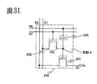
201:電晶體201: Transistor
202:電晶體202: Transistor
203:電晶體203: Transistor
204:電容器204: Capacitor
205:電容器205: capacitor
210:記憶單元陣列210: memory cell array
211:讀出電路211: readout circuit
212:信號線驅動電路212: signal line drive circuit
213:驅動電路213: drive circuit
214:電位產生電路214: Potential generating circuit
215:解碼器215: decoder
216:電晶體216: Transistor
217:電晶體217: Transistor
218:電晶體218: Transistor
219:升壓電路219: Boost circuit
220:類比緩衝器220: analog buffer
221:讀出電路221: readout circuit
223:偏壓電路223: Bias circuit
224:偏壓電路224: Bias circuit
225:參考單元225: Reference Unit
225a:參考單元225a: Reference unit
225b:參考單元225b: Reference unit
225c:參考單元225c: Reference unit
229:邏輯電路229: Logic Circuit
231:讀出電路231: readout circuit
240:記憶單元240: memory unit
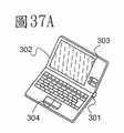
301:主體301: Subject
302:框體302: Frame
303:顯示部303: Display
304:鍵盤304: keyboard
311:主體311: Subject
312:觸控筆312: Stylus
313:顯示部313: Display
314:操作按鈕314: Operation button
315:外部介面315: external interface
320:電子書閱讀器320: e-book reader
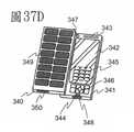
321:框體321: Frame
323:框體323: Frame
325:顯示部325: Display
327:顯示部327: Display
331:電源331: Power
333:操作鍵333: Operation key
335:揚聲器335: Speaker
337:軸部337: Shaft
340:框體340: Frame
341:框體341: Frame
342:顯示面板342: display panel
343:揚聲器343: Speaker
344:麥克風344: Microphone
345:操作鍵345: Operation key
346:指向裝置346: Pointing Device
347:照相用透鏡347: Camera lens
348:外部連接端子348: External connection terminal
349:太陽能電池單元349: Solar cell unit
350:外部記憶體插槽350: External memory slot
361:主體361: Subject
363:取景器363: Viewfinder
364:操作開關364: Operation Switch
365:顯示部(B)365: Display (B)
366:電池366: battery
367:顯示部(A)367: Display (A)
370:電視裝置370: TV installation
371:框體371: Frame
373:顯示部373: Display
375:支架375: Bracket
377:顯示部377: Display
379:操作鍵379: Operation key
380:遙控器380: remote control
402:二極體402: Diode
404:二極體404: Diode
406:二極體406: Diode
408:二極體408: Diode
410:二極體410: Diode
412:電容器412: capacitor
414:電容器414: Capacitor
416:電容器416: capacitor
418:電容器418: Capacitor
420:電容器420: capacitor
在附圖中:In the attached picture:
圖1是用來說明半導體裝置的電路圖;FIG. 1 is a circuit diagram for explaining the semiconductor device;
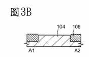
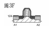
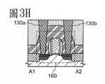
圖2A和圖2B是分別用來說明半導體裝置的截面圖及平面圖;2A and 2B are respectively a cross-sectional view and a plan view for explaining the semiconductor device;
圖3A至圖3H是用來說明半導體裝置的製造製程的截面圖;3A to 3H are cross-sectional views for explaining the manufacturing process of the semiconductor device;
圖4A至圖4G是用來說明半導體裝置的製造製程的截面圖;4A to 4G are cross-sectional views for explaining the manufacturing process of the semiconductor device;
圖5A至圖5D是用來說明半導體裝置的製造製程的截面圖;5A to 5D are cross-sectional views for explaining the manufacturing process of the semiconductor device;
圖6是使用氧化物半導體形成的電晶體的截面圖;6 is a cross-sectional view of a transistor formed using an oxide semiconductor;
圖7是沿著圖6的截面A-A’的能帶圖(示意圖);Fig. 7 is an energy band diagram (schematic diagram) along the section A-A' of Fig. 6;
圖8A是示出對閘極電極(GE)施加正電壓(VG>0)的狀態的圖;圖8B是示出對閘極電極(GE)施加負電位(VG<0)的狀態的圖;FIG. 8A is a diagram showing a state where a positive voltage (VG > 0) is applied to the gate electrode (GE); FIG. 8B is a diagram showing a state where a negative potential (VG <0) is applied to the gate electrode (GE) Figure;
圖9是示出真空能級和金屬的功函數(ΦM)、氧化物半導體的電子親和力(χ)的關係的圖;9 is a graph showing the relationship between the vacuum energy level and the work function (ΦM ) of the metal, and the electron affinity (χ) of the oxide semiconductor;
圖10是示出C-V特性的圖;Fig. 10 is a graph showing C-V characteristics;
圖11是示出Vg和(1/C)2的關係的圖;FIG. 11 is a diagram showing the relationship between Vg and (1/C)2 ;
圖12是用來說明半導體裝置的截面圖;FIG. 12 is a cross-sectional view for explaining the semiconductor device;
圖13A和圖13B是用來說明半導體裝置的截面圖;13A and 13B are cross-sectional views for explaining the semiconductor device;
圖14A和圖14B是用來說明半導體裝置的截面圖;14A and 14B are cross-sectional views for explaining the semiconductor device;
圖15A和圖15B是用來說明半導體裝置的截面圖;15A and 15B are cross-sectional views for explaining the semiconductor device;
圖16是用來說明記憶元件的電路圖;Figure 16 is a circuit diagram for explaining the memory element;
圖17是用來說明半導體裝置的電路圖;FIG. 17 is a circuit diagram for explaining the semiconductor device;
圖18是用來說明驅動電路的電路圖;FIG. 18 is a circuit diagram for explaining the driving circuit;
圖19是用來說明驅動電路的電路圖;FIG. 19 is a circuit diagram for explaining the driving circuit;
圖20是用來說明讀出電路的電路圖;FIG. 20 is a circuit diagram for explaining the readout circuit;
圖21是用來說明電位產生電路的電路圖;FIG. 21 is a circuit diagram for explaining the potential generating circuit;
圖22A和圖22B是用來說明升壓電路的電路圖;22A and 22B are circuit diagrams for explaining the booster circuit;
圖23是用來說明差動感測放大器的電路圖;Figure 23 is a circuit diagram for explaining a differential sense amplifier;
圖24是用來說明鎖存感測放大器的電路圖;Figure 24 is a circuit diagram used to illustrate the latch sense amplifier;
圖25A和圖25B是示出用來說明工作的時序圖的圖;25A and 25B are diagrams showing a timing chart for explaining the operation;
圖26是用來說明半導體裝置的電路圖;FIG. 26 is a circuit diagram for explaining the semiconductor device;
圖27是用來說明讀出電路的電路圖;Figure 27 is a circuit diagram for explaining the readout circuit;
圖28是示出用來說明工作的時序圖的圖;FIG. 28 is a diagram showing a timing chart for explaining the work;
圖29是用來說明讀出電路的圖;Figure 29 is a diagram for explaining the readout circuit;
圖30是示出用來說明工作的時序圖的圖;FIG. 30 is a diagram showing a timing chart for explaining the work;
圖31是用來說明記憶元件的電路圖;Figure 31 is a circuit diagram for explaining the memory element;
圖32是用來說明半導體裝置的電路圖;FIG. 32 is a circuit diagram for explaining the semiconductor device;
圖33是用來說明讀出電路的電路圖;FIG. 33 is a circuit diagram for explaining the readout circuit;
圖34是用來說明驅動電路的電路圖;FIG. 34 is a circuit diagram for explaining the driving circuit;
圖35是示出用來說明工作的時序圖的圖;FIG. 35 is a diagram showing a timing chart for explaining the work;
圖36是示出節點A和字線電位的關係的圖;FIG. 36 is a diagram showing the relationship between the node A and the word line potential;
圖37A至圖37F是用來說明電子設備的圖。37A to 37F are diagrams for explaining electronic equipment.
下面,關於本發明的實施例的一個例子參照附圖給予說明。但是,本發明並不侷限於下面的描述。所屬領域的普通技術人員可以很容易地理解一個事實就是其方式和詳細內容可以被變換為各種各樣的形式,而不脫離本發明的宗旨及其範圍。因此,本發明不應該解釋為侷限於以下所示的實施例的記載內容。Hereinafter, an example of an embodiment of the present invention will be described with reference to the drawings. However, the present invention is not limited to the following description. Those of ordinary skill in the art can easily understand the fact that the method and details can be transformed into various forms without departing from the purpose and scope of the present invention. Therefore, the present invention should not be interpreted as being limited to the description of the embodiments shown below.
注意,為了便於說明,附圖等所示出的各結構的位置、大小和範圍等有時不表示實際上的位置、大小和範圍等。因此,本發明不侷限於附圖等所示出的位置、大小和範圍等。Note that for convenience of description, the positions, sizes, and ranges of each structure shown in the drawings and the like sometimes do not indicate the actual positions, sizes, and ranges. Therefore, the present invention is not limited to the position, size, range, etc. shown in the drawings and the like.
另外,本說明書等中使用的“第一”、“第二”、“第三”等序數詞用來避免結構要素的混同,而不用來在數目方面上限定。In addition, the ordinal numbers such as "first", "second", and "third" used in this specification are used to avoid the confusion of structural elements, and are not used inThe number is limited.
實施例1Example 1
在本實施例中,參照圖1至圖15B說明根據所公開的發明的一個實施例的半導體裝置的結構及其製造方法。In this embodiment, a structure of a semiconductor device and a manufacturing method thereof according to an embodiment of the disclosed invention will be described with reference to FIGS. 1 to 15B.
<半導體裝置的電路結構><Circuit Structure of Semiconductor Device>
圖1示出半導體裝置的電路結構的一個例子。該半導體裝置由使用氧化物半導體以外的材料形成的電晶體160和使用氧化物半導體形成的電晶體162構成。注意,在圖1中,為了明瞭地示出使用氧化物半導體形成電晶體162,而附上OS的符號。FIG. 1 shows an example of the circuit structure of a semiconductor device. This semiconductor device is composed of a
這裏,電晶體160的閘極電極與電晶體162的源極電極和汲極電極中的一個電連接。另外,第一佈線(1st Line:也稱為源極電極線)與電晶體160的源極電極電連接,第二佈線(2nd Line:也稱為位元線)與電晶體160的汲極電極電連接。並且,第三佈線(3rd Line:也稱為第一信號線)與電晶體162的源極電極和汲極電極中的另一個電連接,第四佈線(4th Line:也稱為第二信號線)和電晶體162的閘極電極電連接。Here, the gate electrode of the
使用氧化物半導體以外的材料形成的電晶體160能夠進行充分的高速工作,因此藉由使用該使用氧化物半導體以外的材料形成的電晶體160而可以高速讀出儲存內容。另外,使用氧化物半導體形成的電晶體162具有截止電流極小的特徵。因此,藉由使電晶體162處於截止狀態,可以在極長時間內保持電晶體160的閘極電極的電位。The
藉由發揮能夠長時間保持閘極電極的電位的特徵,如下所述那樣可以進行資訊寫入、保持和讀出。By taking advantage of the feature of being able to maintain the potential of the gate electrode for a long time, information can be written, held, and read as described below.
說明資訊的寫入及保持。首先,藉由將第四佈線的電位設定為使電晶體162處於導通狀態的電位,使電晶體162處於導通狀態。由此,將第三佈線的電位施加到電晶體160的閘極電極(寫入)。然後,藉由將第四佈線的電位設定為使電晶體162處於截止狀態的電位,使電晶體162處於截止狀態,而保持電晶體160的閘極電極的電位(保持)。Explain the writing and keeping of information. First, by setting the potential of the fourth wiring to the potential at which the
因為電晶體162的截止電流極小,所以在長時間內保持電晶體160的閘極電極的電位。例如,在電晶體160的閘極電極的電位為使電晶體160處於導通狀態的電位的情況下,在長時間內保持電晶體160的導通狀態。另外,在電晶體160的閘極電極的電位為使電晶體160處於截止狀態的電位的情況下,在長時間內保持電晶體160的截止狀態。Since the off current of the
下面,說明資訊的讀出。如上所述,當在保持電晶體160的導通狀態或截止狀態的狀態下將預定的電位(低電位)施加到第一佈線時,第二佈線的電位根據電晶體160的導通狀態或截止狀態而成為不同的值。例如,在電晶體160處於導通狀態的情況下,第二佈線的電位根據第一佈線的電位而降低。與此相反,在電晶體160處於截止狀態的情況下,第二佈線的電位不變化。Next, the reading of information will be explained. As described above, when a predetermined potential (low potential) is applied to the first wiring while maintaining the on state or off state of the
如上所述,藉由在保持資訊的狀態下對第一佈線的電位和第二佈線的電位進行比較,可以讀出資訊。As described above, by comparing the potential of the first wiring with the potential of the second wiring while maintaining the information, the information can be read.
下面,說明資訊的重寫。與上述資訊的寫入及保持同樣,進行資訊的重寫。就是說,藉由將第四佈線的電位設定為使電晶體162處於導通狀態的電位,使電晶體162處於導通狀態。由此,將第三佈線的電位(根據新的資訊的電位)施加到電晶體160的閘極電極。然後,藉由將第四佈線的電位設定為使電晶體162處於截止狀態的電位,使電晶體162處於截止狀態,而處於保持新的資訊的狀態。Next, the rewriting of information will be explained. Similar to the writing and holding of the above information, the information is rewritten. That is, by setting the potential of the fourth wiring to a potential at which the
如上所述,根據所公開的發明的半導體裝置可以藉由再次寫入資訊而直接重寫資訊。由此,不需要快閃記憶體等所需要的擦除工作,而可以抑制起因於擦除工作的工作速度的降低。就是說,實現半導體裝置的高速工作。As described above, the semiconductor device according to the disclosed invention can directly rewrite information by rewriting the information. As a result, the erasing work required for flash memory or the like is not required, and it is possible to suppress a decrease in the operation speed due to the erasing operation. In other words, high-speed operation of the semiconductor device is realized.
另外,上述說明關於使用以電子為載子的n型電晶體(n通道型電晶體)的情況,但是,當然可以使用以電洞為載子的p型電晶體代替n型電晶體。In addition, the above description is about the case of using an n-type transistor (n-channel type transistor) that uses electrons as carriers, but it is of course possible to use a p-type transistor that uses holes as a carrier instead of the n-type transistor.
另外,為了容易保持電晶體160的閘極電極的電位,當然可以對電晶體160的閘極電極附加電容器等。In addition, in order to easily maintain the potential of the gate electrode of the
<半導體裝置的平面結構及截面結構><Plane structure and cross-sectional structure of semiconductor device>
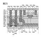
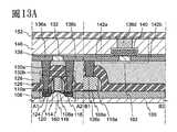
圖2A和圖2B是上述半導體裝置的結構的一個例子。圖2A示出半導體裝置的截面,而圖2B示出半導體裝置的平面。這裏,圖2A相當於沿圖2B的線A1-A2及線B1-B2的截面。圖2A和圖2B所示的半導體裝置在其下部具有使用氧化物半導體以外的材料形成的電晶體160並在其上部具有使用氧化物半導體形成的電晶體162。這裏,說明電晶體160及電晶體162都是n型電晶體的情況,但是也可以採用p型電晶體。尤其是,電晶體160可以為p型電晶體。2A and 2B are an example of the structure of the above-mentioned semiconductor device. FIG. 2A shows a cross section of the semiconductor device, and FIG. 2B shows a plane of the semiconductor device. Here, Figure 2A corresponds to the line A1-A2 andSection of line B1-B2. The semiconductor device shown in FIGS. 2A and 2B has a
電晶體160具有:設置在包含半導體材料的基板100中的通道形成區116;夾持通道形成區116地設置的雜質區114及高濃度雜質區120(也將這些區域總稱為雜質區);設置在通道形成區116上的閘極絕緣層108a;設置在閘極絕緣層108a上的閘極電極110a;電連接到設置在通道形成區116的一側的雜質區114的源極電極或汲極電極130a;以及電連接到設置在通道形成區116的另一側的雜質區114的源極電極或汲極電極130b。The
這裏,在閘極電極110a的側面設置有側壁絕緣層118。另外,在基板100上具有當從上面觀察時夾著側壁絕緣層118地設置的高濃度雜質區120,並且在高濃度雜質區120上存在著金屬化合物區124。另外,在基板100上圍繞p型電晶體160地設置有元件分離絕緣層106,並且覆蓋p型電晶體160地設置有層間絕緣層126及層間絕緣層128。藉由形成在層間絕緣層126及層間絕緣層128中的開口,源極電極或汲極電極130a電連接到設置在通道形成區116的一側的金屬化合物區124,並且源極電極或汲極電極130b電連接到設置在通道形成區116的另一側的金屬化合物區124。就是說,源極電極或汲極電極130a藉由設置在通道形成區116的一側的金屬化合物區124而電連接到設置在通道形成區116的一側的高濃度雜質區120及設置在通道形成區116的一側的雜質區114,並且源極電極或汲極電極130b藉由設置在通道形成區116的另一側的金屬化合物區124而電連接到設置在通道形成區116的另一側的高濃度雜質區120及設置在通道形成區116的另一側的雜質區114。另外,閘極電極110a電連接到與源極電極或汲極電極130a以及源極電極或汲極電極130b同樣設置的電極130c。Here, a
電晶體162具有:設置在層間絕緣層128上的閘極電極136d;設置在閘極電極136d上的閘極絕緣層138;設置在閘極絕緣層138上的氧化物半導體層140;設置在氧化物半導體層140上且電連接到氧化物半導體層140的源極電極或汲極電極142a;以及源極電極或汲極電極142b。The
這裏,閘極電極136d設置為埋入形成在層間絕緣層128上的絕緣層132。另外,與閘極電極136d同樣,分別形成有接觸於源極電極或汲極電極130a的電極136a、接觸於源極電極或汲極電極130b的電極136b以及接觸於電極130c的電極136c。Here, the
另外,在電晶體162上接觸於氧化物半導體層140的一部分地設置有保護絕緣層144,在保護絕緣層144上設置有層間絕緣層146。這裏,在保護絕緣層144和層間絕緣層146中設置有到達源極電極或汲極電極142a、源極電極或汲極電極142b的開口,並且以藉由該開口接觸於源極電極或汲極電極142a以及源極電極或汲極電極142b的方式形成有電極150d及電極150e。另外,與電極150d及電極150e同樣,形成有藉由設置在閘極絕緣層138、保護絕緣層144和層間絕緣層146中的開口接觸於電極136a、電極136b以及電極136c的電極150a、電極150b以及電極150c。In addition, a protective
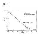
這裏,氧化物半導體層140最好為雜質如氫等充分得到去除而被高純度化的氧化物半導體層。明確地說,氧化物半導體層140的氫濃度為小於或等於5×10¹⁹atoms/cm3,最好為小於或等於5×1018atoms/cm3,更佳地為小於或等於5×1017atoms/cm3。另外,氧化物半導體層140最好為藉由含有充分的氧而起因於氧缺乏的缺陷減少的氧化物半導體層。氫濃度充分得到降低而被高純度化的氧化物半導體層140的載子濃度是小於或等於1×1012/cm3,最好是小於或等於1×1011/cm3。如上所述,藉由使用被i型化(本質化)或實際上被i型化的氧化物半導體,可以獲得截止電流特性極為優良的電晶體162。例如,在汲極電極電壓Vd為+1V或+10V且閘極電壓Vg為-5V至-20V的情況下,截止電流為小於或等於1×10-13A。如上所述,藉由使用氫濃度充分得到降低而被高純度化且起因於氧缺乏的缺陷減少的氧化物半導體層140而降低電晶體162的截止電流,可以實現新的結構的半導體裝置。另外,使用二次離子質譜(SIMS:Secondary Ion Mass Spectroscopy)測量上述氧化物半導體層140中的氫濃度。Here, the
另外,在層間絕緣層146上設置有絕緣層152,並埋入該絕緣層152地設置有電極154a、電極154b、電極154c以及電極154d。這裏,電極154a接觸於電極150a,電極154b接觸於電極150b,電極154c接觸於電極150c及電極150d,並且電極154d接觸於電極150e。In addition, an insulating
就是說,在圖2A和圖2B所示的半導體裝置中,電晶體160的閘極電極110a隔著電極130c、電極136c、電極150c、電極154c以及電極150d電連接到電晶體162的源極電極或汲極電極142a。That is, in the semiconductor device shown in FIGS. 2A and 2B, the
<半導體裝置的製造方法><Method of Manufacturing Semiconductor Device>
接著,說明上述半導體裝置的製造方法的一個例子。以下,首先,參照圖3A至圖3H說明下部的電晶體160的製造方法,然後,參照圖4A至圖4G和圖5A至圖5D說明上部的電晶體162的製造方法。Next, an example of a method of manufacturing the above-mentioned semiconductor device will be described. Hereinafter, first, the method of manufacturing the
<下部的電晶體的製造方法><Method of Manufacturing Lower Transistor>
首先,準備包含半導體材料的基板100(參照圖3A)。作為包含半導體材料的基板100,可以使用矽或碳化矽等的單晶半導體基板、多晶半導體基板、矽鍺等的化合物半導體基板、SOI基板等。這裏,示出作為包含半導體材料的基板100,使用單晶矽基板時的一個例子。一般來說,“SOI基板”是指在絕緣表面上設置有矽半導體層的基板,但是在本說明書等中,“SOI基板”還包括在絕緣表面上設置有由矽以外的材料構成的半導體層的基板。換言之,“SOI基板”所具有的半導體層不侷限於矽半導體層。另外,SOI基板還包括在玻璃基板等的絕緣基板上隔著絕緣層而設置有半導體層的基板。First, a
在基板100上形成用作用來形成元件分離絕緣層的掩模的保護層102(參照圖3A)。作為保護層102,例如可以使用以氧化矽、氮化矽、氮氧化矽等為其材料的絕緣層。另外,在該製程的前後,也可以將賦予n型導電性的雜質元素或賦予p型導電性的雜質元素添加到基板100,以控制電晶體的臨界值電壓。在半導體為矽時,作為賦予n型導電性的雜質,例如可以使用磷、砷等。另外,作為賦予p型導電性的雜質,例如可以使用硼、鋁、鎵等。A
接著,使用上述保護層102作為掩模進行蝕刻,去除不由保護層102覆蓋的區域(露出的區域)的基板100的一部分。由此,形成得到分離的半導體區104(參照圖3B)。該蝕刻最好使用乾蝕刻,但是也可以使用濕蝕刻。可以根據被蝕刻材料適當地選擇蝕刻氣體、蝕刻液。Next, etching is performed using the
接著,覆蓋半導體區104地形成絕緣層,並且藉由選擇性地去除重疊於半導體區104的區域的絕緣層,形成元件分離絕緣層106(參照圖3B)。該絕緣層使用氧化矽、氮化矽、氮氧化矽等而形成。作為絕緣層的去除方法,有CMP等拋光處理或蝕刻等,可以使用任何方法。另外,在形成半導體區104之後,或者,在形成元件分離絕緣層106之後,去除上述保護層102。Next, an insulating layer is formed to cover the
接著,在半導體區104上形成絕緣層,並在該絕緣層上形成包含導電材料的層。Next, an insulating layer is formed on the
絕緣層是之後成為閘極絕緣層的層,該絕緣層最好採用藉由CVD法或濺射法等來得到的包含氧化矽、氮氧化矽、氮化矽、氧化鉿、氧化鋁、氧化鉭等的膜的單層結構或疊層結構。另外,也可以藉由高密度電漿處理或熱氧化處理使半導體區104的表面氧化或氮化,形成上述絕緣層。例如,可以使用He、Ar、Kr、Xe等稀有氣體和氧、氧化氮、氨、氮、氫等的混合氣體來進行高密度電漿處理。另外,對絕緣層的厚度沒有特別的限制,例如可以將其厚度設定為大於或等於1nm且小於或等於100nm。The insulating layer is the layer that will become the gate insulating layer. The insulating layer is preferably obtained by CVD or sputtering, including silicon oxide, silicon oxynitride, silicon nitride, hafnium oxide, aluminum oxide, and tantalum oxide. Such as single-layer structure or laminated structure of the film. In addition, the surface of the
包含導電材料的層可以使用鋁、銅、鈦、鉭、鎢等的金屬材料而形成。另外,也可以藉由使用包含導電材料的多晶矽等的半導體材料形成包含導電材料的層。對形成方法也沒有特別的限制,可以使用蒸鍍法、CVD法、濺射法、旋塗法等的各種沉積方法。此外,在本實施例中,說明使用金屬材料形成包含導電材料的層時的一個例子。The layer containing a conductive material can be formed using metal materials such as aluminum, copper, titanium, tantalum, and tungsten. In addition, a layer containing a conductive material may be formed by using a semiconductor material such as polysilicon containing a conductive material. The formation method is not particularly limited, and various deposition methods such as vapor deposition, CVD, sputtering, and spin coating can be used. In addition, in this embodiment, an example when a metal material is used to form a layer containing a conductive material is described.
然後,藉由選擇性地蝕刻絕緣層和包含導電材料的層,形成閘極絕緣層108a和閘極電極110a。(參照圖3C)。Then, by selectively etching the insulating layer and the layer containing the conductive material, the
接著,形成覆蓋閘極電極110a的絕緣層112(參照圖3C)。然後,藉由將磷(P)或砷(As)等添加到半導體區104,形成接面深度淺的雜質區114(參照圖3C)。這裏,雖然添加磷或砷以形成n型電晶體,但是在形成p型電晶體時添加硼(B)或鋁(Al)等的雜質元素即可。另外,藉由形成雜質區114,在半導體區104的閘極絕緣層108a的下部形成通道形成區116(參照圖3C)。在此,雖然可以適當地設定所添加的雜質的濃度,但是在進行半導體元件的高微細化時最好提高其濃度。這裏,雖然採用在形成絕緣層112之後形成雜質區114的製程,但是也可以採用在形成雜質區114之後形成絕緣層112的製程。Next, an insulating
接著,形成側壁絕緣層118(參照圖3D)。藉由在覆蓋絕緣層112地形成絕緣層之後,對該絕緣層進行各向異性高的蝕刻,可以以自對準的方式形成側壁絕緣層118。另外,此時,最好對絕緣層112的一部分進行蝕刻,而使閘極電極110a的上面和雜質區114的上面露出。Next, a
接著,覆蓋閘極電極110a、雜質區114和側壁絕緣層118等地形成絕緣層。然後,藉由將磷(P)或砷(As)等添加到該絕緣層接觸於雜質區114的區域,形成高濃度雜質區120(參照圖3E)。然後,去除上述絕緣層,覆蓋閘極電極110a、側壁絕緣層118和高濃度雜質區120等地形成金屬層122(參照圖3E)。該金屬層122可以使用真空蒸鍍法、濺射法或旋塗法等的各種沉積方法形成。最好使用與構成半導體區104的半導體材料起反應而成為低電阻的金屬化合物的金屬材料形成金屬層122。作為上述金屬材料,例如有鈦、鉭、鎢、鎳、鈷、鉑等。Next, an insulating layer is formed to cover the
接著,進行熱處理,使上述金屬層122與半導體材料起反應。由此,形成接觸於高濃度雜質區120的金屬化合物區124(參照圖3F)。另外,在使用多晶矽等作為閘極電極110a的情況下,還在閘極電極110a與金屬層122接觸的部分中形成金屬化合物區。Next, heat treatment is performed to make the
作為上述熱處理,例如可以使用照射閃光燈的熱處理。當然,也可以使用其他熱處理方法,但是最好使用可以在極短的時間內進行熱處理的方法,以提高關於金屬化合物形成的化學反應的控制性。另外,上述金屬化合物區124由金屬材料與半導體材料之間的反應而形成,該金屬化合物區的導電性充分得到提高。藉由形成該金屬化合物區124,可以充分降低電阻,並可以提高元件特性。另外,在形成金屬化合物區124之後,去除金屬層122。As the above-mentioned heat treatment, for example, heat treatment of irradiating a flash lamp can be used. Of course, other heat treatment methods can also be used, but it is best to use a method that can be heat treated in a very short time to improve the controllability of the chemical reaction formed by the metal compound. In addition, the
接著,覆蓋藉由上述製程形成的各結構地形成層間絕緣層126和層間絕緣層128(參照圖3G)。層間絕緣層126和層間絕緣層128可以使用包含氧化矽、氮氧化矽、氮化矽、氧化鉿、氧化鋁、氧化鉭等無機絕緣材料的材料形成。此外,也可以使用聚醯亞胺、丙烯酸樹脂等有機絕緣材料形成層間絕緣層126和層間絕緣層128。這裏,雖然示出層間絕緣層126和層間絕緣層128的兩層結構,但是層間絕緣層的結構不侷限於此。在形成層間絕緣層128之後,最好藉由CMP或蝕刻等而使其表面平坦化。Next, an
然後,藉由在上述層間絕緣層中形成到達金屬化合物區124的開口,在該開口中形成源極電極或汲極電極130a和源極電極或汲極電極130b(參照圖3H)。例如,可以在包括開口的區域中使用PVD法或CVD法等形成導電層,然後使用蝕刻或CMP等的方法去除上述導電層的一部分,而形成源極電極或汲極電極130a和源極電極或汲極電極130b。Then, by forming an opening reaching the
另外,在去除上述導電層的一部分形成源極電極或汲極電極130a、源極電極或汲極電極130b時,最好將其表面加工為平坦。例如,當在包括開口的區域中形成薄的鈦膜或氮化鈦膜,然後將鎢膜形成為嵌入開口中時,藉由進行之後的CMP,可以在去除多餘的鎢膜、鈦膜、氮化鈦膜等的同時提高其表面的平坦性。像這樣,藉由對包括源極電極或汲極電極130a、源極電極或汲極電極130b的表面進行平坦化,可以在之後的製程中形成優良的電極、佈線、絕緣層或半導體層等。In addition, when a part of the above-mentioned conductive layer is removed to form the source electrode or
這裏,雖然附圖僅示出接觸於金屬化合物區124的源極電極或汲極電極130a、源極電極或汲極電極130b,但是也可以在該製程中形成接觸於閘極電極110a的電極(例如,圖2A中的電極130c)等。對可以用作源極電極或汲極電極130a、源極電極或汲極電極130b的材料沒有特別的限制,而可以使用各種導電材料。例如,可以使用鉬、鈦、鉻、鉭、鎢、鋁、銅、釹或鈧等導電材料。Here, although the drawings only show the source electrode or
藉由上述製程,形成使用包含半導體材料的基板100形成的電晶體160。另外,在進行上述製程之後,還可以形成電極、佈線或絕緣層等。藉由使用由層間絕緣層和導電層的疊層結構構成的多層佈線結構作為佈線的結構,可以提供高集成化的半導體裝置。Through the above process, a
<上部的電晶體的製造方法><Method of manufacturing upper transistor>
接著,參照圖4A至圖4G及圖5A至圖5D說明在層間絕緣層128上製造電晶體162的製程。另外,圖4A至圖4G及圖5A至圖5D示出層間絕緣層128上的各種電極或電晶體162等的製造製程,而省略存在於電晶體162的下部的電晶體160等。Next, the process of manufacturing the
首先,在層間絕緣層128、源極電極或汲極電極130a、源極電極或汲極電極130b以及電極130c上形成絕緣層132(參照圖4A)。絕緣層132可以使用PVD法或CVD法等而形成。另外,可以使用包含氧化矽、氮氧化矽、氮化矽、氧化鉿、氧化鋁、氧化鉭等無機絕緣材料的材料形成絕緣層132。First, an insulating
接著,在絕緣層132中形成到達源極電極或汲極電極130a、源極電極或汲極電極130b以及電極130c的開口。此時,還在之後形成閘極電極136d的區域中形成開口。然後,將導電層134形成為嵌入上述開口中(參照圖4B)。上述開口可以使用掩模藉由蝕刻等的方法而形成。上述掩模可以藉由使用光掩模的曝光等的方法而形成。作為蝕刻,可以使用濕蝕刻或乾蝕刻,但是從微細加工的觀點來看,最好使用乾蝕刻。導電層134可以使用PVD法或CVD法等的沉積法而形成。作為可以用來形成導電層134的材料,可以舉出鉬、鈦、鉻、鉭、鎢、鋁、銅、釹或鈧等導電材料、該材料的合金或化合物(例如,氮化物)等。Next, an opening that reaches the source electrode or
更明確地說,例如可以使用如下方法,即:在包括開口的區域中使用PVD法形成薄的鈦膜,並且使用CVD法形成薄的氮化鈦膜,然後將鎢膜形成為嵌入開口中的方法。這裏,藉由PVD法形成的鈦膜具有使介面的氧化膜還原並降低其與下部電極(這裏,源極電極或汲極電極130a、源極電極或汲極電極130b、電極130c等)的接觸電阻的功能。另外,之後形成的氮化鈦膜具有抑制導電材料的擴散的阻擋功能。另外,也可以在形成由鈦或氮化鈦等構成的障壁膜之後,使用鍍法形成銅膜。More specifically, for example, a method of forming a thin titanium film using a PVD method in a region including an opening, and forming a thin titanium nitride film using a CVD method, and then forming a tungsten film to be embedded in the opening method. Here, the titanium film formed by the PVD method reduces the oxide film of the interface and reduces its contact with the lower electrode (here, the source electrode or
在形成導電層134之後,藉由使用蝕刻或CMP等的方法去除導電層134的一部分,使絕緣層132露出,而形成電極136a、電極136b、電極136c以及閘極電極136d(參照圖4C)。另外,在去除上述導電層134的一部分而形成電極136a、電極136b、電極136c以及閘極電極136d時,最好將其表面加工為平坦。如此,藉由將絕緣層132、電極136a、電極136b、電極136c以及閘極電極136d的表面加工為平坦,可以在之後的製程中形成優良的電極、佈線、絕緣層以及半導體層等。After the
接著,覆蓋絕緣層132、電極136a、電極136b、電極136c以及閘極電極136d地形成閘極絕緣層138(參照圖4D)。閘極絕緣層138可以藉由CVD法或濺射法等形成。另外,閘極絕緣層138最好包含氧化矽、氮化矽、氧氮化矽、氮氧化矽、氧化鋁、氧化鉿或氧化鉭等。另外,閘極絕緣層138可以具有單層結構或者疊層結構。例如,藉由作為原料氣體使用矽烷(SiH4)、氧和氮的電漿CVD法,可以形成包含氧氮化矽的閘極絕緣層138。對閘極絕緣層138的厚度沒有特別的限制,例如可以將其厚度設定為大於或等於10nm且小於或等於500nm。在使用疊層結構時,例如,最好使用由厚度為大於或等於50nm且小於或等於200nm的第一閘極絕緣層和第一閘極絕緣層上的厚度為大於或等於5nm且小於或等於300nm的第二閘極絕緣層構成的疊層。Next, a
另外,因為藉由去除雜質而被i型化或者在實際上被i型化的氧化物半導體(高純度化的氧化物半導體)對介面能級或介面電荷極為敏感,所以在作為氧化物半導體層使用該氧化物半導體的情況下,其與閘極絕緣層的介面是重要的。就是說,接觸於被高純度化的氧化物半導體層的閘極絕緣層138被要求高品質化。In addition, since the oxide semiconductor (high-purity oxide semiconductor) that is i-typed by removing impurities or is actually i-typed is extremely sensitive to the interface energy level or interface charge, it is used as an oxide semiconductor layer In the case of using this oxide semiconductor, its interface with the gate insulating layer is important. In other words, the
另外,因為藉由使用微波(2.45GHz)的高密度電漿CVD法而可以形成緻密且絕緣耐壓高的高品質的閘極絕緣層138,所以該方法是較佳的。這是因為如下緣故:高純度化的氧化物半導體層與高品質閘極絕緣層密接,使得介面能級得到降低而可以得到優良的介面特性。In addition, since the high-density plasma CVD method using microwaves (2.45 GHz) can form a dense and high-quality
當然,只要是能夠作為閘極絕緣層形成優質的絕緣層的方法,就在使用高純度化的氧化物半導體層的情況下也可以使用濺射法或電漿CVD法等的其他方法。另外,也可以使用藉由形成後的熱處理而使膜品質或與氧化物半導體層的介面特性得到改善的絕緣層。無論在哪種情況下,形成作為閘極絕緣層138的膜品質優良且可以降低與氧化物半導體層的介面態密度而形成優良的介面的閘極絕緣層,即可。Of course, as long as it is a method capable of forming a high-quality insulating layer as a gate insulating layer, other methods such as a sputtering method or a plasma CVD method can also be used when a highly purified oxide semiconductor layer is used. In addition, it is also possible to use an insulating layer whose film quality or interface characteristics with the oxide semiconductor layer are improved by heat treatment after formation. In either case, it is sufficient to form a gate insulating layer that has good film quality as the
再者,在溫度為85℃,電場強度為2×10⁶V/cm且時間為12小時的閘極偏壓-熱應力試驗(稱為BT試驗)中,如果在氧化物半導體中添加有雜質,雜質和氧化物半導體的主要成分之間的鍵被強電場(B:偏壓)和高溫(T:溫度)切斷,產生的懸空鍵導致臨界值電壓(Vth)的漂移。Furthermore, in the gate bias-thermal stress test (called BT test) with a temperature of 85°C, an electric field intensity of 2×10⁶ V/cm and a time of 12 hours, if impurities are added to the oxide semiconductor , The bond between the impurity and the main component of the oxide semiconductor is cut off by a strong electric field (B: bias) and high temperature (T: temperature), and the resulting dangling bond causes a shift in the threshold voltage (Vth).
與此相反,藉由儘量去除氧化物半導體中的雜質,尤其是氫或水等,如上所述那樣使與閘極絕緣層的介面特性優良,而可以得到對BT試驗也穩定的電晶體。On the contrary, by removing impurities in the oxide semiconductor as much as possible, especially hydrogen or water, as described above, the interface characteristics with the gate insulating layer are excellent, and a transistor that is stable to the BT test can be obtained.
接著,在閘極絕緣層138上形成氧化物半導體層,藉由使用掩模的蝕刻等方法而加工該氧化物半導體層,而形成島狀的氧化物半導體層140(參照圖4E)。Next, an oxide semiconductor layer is formed on the
作為氧化物半導體層,可以採用使用如下材料的氧化物半導體層,該材料是:四元金屬氧化物的In-Sn-Ga-Zn-O;三元金屬氧化物的In-Ga-Zn-O、In-Sn-Zn-O、In-Al-Zn-O、Sn-Ga-Zn-O、Al-Ga-Zn-O、Sn-Al-Zn-O;二元金屬氧化物的In-Zn-O、Sn-Zn-O、Al-Zn-O、Zn-Mg-O、Sn-Mg-O、In-Mg-O;以及單元金屬氧化物的In-O、Sn-O、Zn-O等。另外,也可以使上述氧化物半導體材料包含SiO2。As the oxide semiconductor layer, an oxide semiconductor layer using the following materials may be used: In-Sn-Ga-Zn-O of quaternary metal oxide; In-Ga-Zn-O of ternary metal oxide , In-Sn-Zn-O, In-Al-Zn-O, Sn-Ga-Zn-O, Al-Ga-Zn-O, Sn-Al-Zn-O; In-Zn binary metal oxide -O, Sn-Zn-O, Al-Zn-O, Zn-Mg-O, Sn-Mg-O, In-Mg-O; and In-O, Sn-O, Zn-O of unit metal oxide Wait. In addition, the above-mentioned oxide semiconductor material may contain SiO2 .
作為氧化物半導體層,可以使用以InMO3(ZnO)m(m>0)表示的薄膜。在此,M表示選自Ga、Al、Mn及Co中的一種或多種金屬元素。例如,作為M,可以舉出:Ga;Ga及Al;Ga及Mn;或Ga及Co等。在具有表示為InMO3(ZnO)m(m>0)的結構的氧化物半導體膜中,將具有作為M而包含Ga的結構的氧化物半導體稱為In-Ga-Zn-O類氧化物半導體,並將其薄膜稱為In-Ga-Zn-O類氧化物半導體膜(In-Ga-Zn-O類非晶膜)等。As the oxide semiconductor layer, a thin film represented by InMO3 (ZnO)m (m>0) can be used. Here, M represents one or more metal elements selected from Ga, Al, Mn, and Co. For example, as M, Ga; Ga and Al; Ga and Mn; or Ga and Co, etc. can be mentioned. In an oxide semiconductor film having a structure expressed as InMO3 (ZnO)m (m>0), an oxide semiconductor having a structure containing Ga as M is called an In-Ga-Zn-O-based oxide semiconductor , And its thin film is called In-Ga-Zn-O-based oxide semiconductor film (In-Ga-Zn-O-based amorphous film) and the like.
在本實施例中,使用用來形成In-Ga-Zn-O類氧化物半導體膜的靶並藉由濺射法形成非晶氧化物半導體層作為氧化物半導體層。另外,因為藉由將矽添加到氧化物半導體層中來可以抑制其晶化,所以例如也可以使用包含大於或等於2wt%且小於或等於10wt%的SiO2的靶形成氧化物半導體層。In this embodiment, a target for forming an In-Ga-Zn-O-based oxide semiconductor film is used and an amorphous oxide semiconductor layer is formed by a sputtering method as the oxide semiconductor layer. In addition, since the crystallization of silicon can be suppressed by adding silicon to the oxide semiconductor layer, for example, the oxide semiconductor layer can be formed using a target containing 2 wt% or more and 10 wt% of SiO2 .
作為用來使用濺射法製造氧化物半導體層的靶,例如,可以使用以氧化鋅為主要成分的金屬氧化物的靶。另外,也可以使用包含In、Ga和Zn的用來形成氧化物半導體膜的靶(組成比為In2O3:Ga2O3:ZnO=1:1:1[摩爾比])等。另外,作為包含In、Ga和Zn的用來形成氧化物半導體膜的靶,也可以使用其組成比為In2O3:Ga2O3:ZnO=1:1:2[摩爾比]或In2O3:Ga2O3:ZnO=1:1:4[摩爾比]的靶等。用來形成氧化物半導體膜的靶的填充率為大於或等於90%且小於或等於100%,最好為大於或等於95%(例如,99.9%)。藉由使用填充率高的用來形成氧化物半導體膜的靶,形成緻密的氧化物半導體層。As a target for producing an oxide semiconductor layer using a sputtering method, for example, a target of a metal oxide containing zinc oxide as a main component can be used. In addition, a target for forming an oxide semiconductor film containing In, Ga, and Zn (composition ratio of In2 O3 :Ga2 O3 :ZnO=1:1:1 [molar ratio]) or the like may also be used. In addition, as a target for forming an oxide semiconductor film containing In, Ga, and Zn, the composition ratio of In2 O3 :Ga2 O3 :ZnO=1:1:2 [molar ratio] or In can also be used.2 O3 : Ga2 O3 : ZnO=1:1:4 [molar ratio] target, etc. The filling rate of the target used to form the oxide semiconductor film is 90% or more and 100% or less, preferably 95% or more (for example, 99.9%). By using a target for forming an oxide semiconductor film with a high filling rate, a dense oxide semiconductor layer is formed.
氧化物半導體層的形成氣圍最好為稀有氣體(典型為氬)氣圍、氧氣圍或稀有氣體(典型為氬)和氧的混合氣圍。明確地說,例如,最好使用氫、水、羥基或氫化物等的雜質的濃度降低到幾ppm左右(最好為幾ppb左右)的高純度氣體。The oxide semiconductor layer is preferably formed with a rare gas (typically argon) gas surrounding, an oxygen gas surrounding or a mixed gas surrounding of a rare gas (typically argon) and oxygen. Specifically, for example, it is preferable to use a high-purity gas in which the concentration of impurities such as hydrogen, water, hydroxyl, or hydride is reduced to about several ppm (preferably about several ppb).
在形成氧化物半導體層時,在保持為減壓狀態的處理室內固定基板,並且將基板溫度設定為高於或等於100℃且低於或等於600℃,最好為高於或等於200℃且低於或等於400℃。藉由在加熱基板的同時形成氧化物半導體層,可以降低氧化物半導體層所包含的雜質的濃度。另外,可以減輕由濺射導致的損傷。然後,在去除處理室內的殘留水分的同時引入氫和水得到去除的濺射氣體,並且將金屬氧化物用作靶來形成氧化物半導體層。最好使用吸附型真空泵,以去除處理室內的殘留水分。例如,可以使用低溫泵、離子泵或鈦昇華泵。另外,作為排氣單元,也可以使用提供有冷阱的渦輪泵。在使用低溫泵進行了排氣的沉積室中,例如排出氫原子、水(H2O)等包含氫原子的化合物(更佳的是,還有包含碳原子的化合物)等,因此可以降低在該沉積室中形成的氧化物半導體層所包含的雜質的濃度。When forming the oxide semiconductor layer, the substrate is fixed in a processing chamber maintained in a reduced pressure state, and the substrate temperature is set to be higher than or equal to 100°C and lower than or equal to 600°C, preferably higher than or equal to 200°C and Lower than or equal to 400°C. By forming the oxide semiconductor layer while heating the substrate, the concentration of impurities contained in the oxide semiconductor layer can be reduced. In addition, damage caused by sputtering can be reduced. Then, the sputtering gas from which hydrogen and water are removed is introduced while removing residual moisture in the processing chamber, and the metal oxide is used as a target to form an oxide semiconductor layer. It is best to use an adsorption vacuum pump to remove residual moisture in the processing chamber. For example, a cryopump, ion pump, or titanium sublimation pump can be used. In addition, as the exhaust unit, a turbo pump provided with a cold trap can also be used. In a deposition chamber exhausted with a cryopump, for example, hydrogen atoms, water (H2 O) and other compounds containing hydrogen atoms (preferably, compounds containing carbon atoms) are discharged, so that the The concentration of impurities contained in the oxide semiconductor layer formed in the deposition chamber.
作為形成條件,例如,可以採用如下條件:基板和靶之間的距離為100mm;壓力為0.6Pa;直流(DC)電力為0.5kW;並且氣圍為氧(氧流量比率為100%)氣圍。注意,當使用脈衝直流(DC)電源時,可以減少在形沉積時發生的粉狀物質(也稱為微粒或塵埃),並且膜厚度分佈也變得均勻,所以是較佳的。將氧化物半導體層的厚度設定為大於或等於2nm且小於或等於200nm、最好為大於或等於5nm且小於或等於30nm。另外,因為氧化物半導體層的適當的厚度根據使用的氧化物半導體材料而不同,所以可以根據使用的材料適當地選擇其厚度。As the formation conditions, for example, the following conditions may be adopted: the distance between the substrate and the target is 100mm; the pressure is 0.6Pa; the direct current (DC) power is 0.5kW; and the air enclosure is oxygen (oxygen flow rate is 100%) air enclosure . Note that when a pulsed direct current (DC) power supply is used, it is possible to reduce powdery substances (also called particles or dust) that occur during in-shape deposition, and the film thickness distribution becomes uniform, so it is preferable. The thickness of the oxide semiconductor layer is set to be greater than or equal to 2 nm and less than or equal to 200 nm, preferably greater than or equal to 5 nm and less than or equal to 30 nm. In addition, since the appropriate thickness of the oxide semiconductor layer differs according to the oxide semiconductor material used, the thickness can be appropriately selected according to the material used.
另外,最好在藉由濺射法形成氧化物半導體層之前進行引入氬氣體來產生電漿的反濺射,而去除附著在閘極絕緣層138的表面的塵埃。這裏,在通常的濺射中將離子碰撞到濺射靶的處理,而在反濺射中將離子碰撞到處理表面來改變其表面的性質。作為將離子碰撞到處理表面的方法,有在氬氣圍中將高頻電壓施加到處理表面一側而在基板附近產生電漿的方法等。另外,也可以使用氮氣圍、氦氣圍或氧氣圍等代替氬氣圍。In addition, it is preferable to perform reverse sputtering in which argon gas is introduced to generate plasma before forming the oxide semiconductor layer by the sputtering method to remove dust adhering to the surface of the
作為上述氧化物半導體層的蝕刻可以使用乾蝕刻和濕蝕刻中的任何一種。當然,也可以組合乾蝕刻和濕蝕刻而使用。根據材料適當地設定蝕刻條件(蝕刻氣體、蝕刻液、蝕刻時間、溫度等),以將其蝕刻成所希望的形狀。As the etching of the above-mentioned oxide semiconductor layer, any of dry etching and wet etching can be used. Of course, dry etching and wet etching can also be used in combination. The etching conditions (etching gas, etching solution, etching time, temperature, etc.) are appropriately set according to the material to etch it into a desired shape.
作為用於乾蝕刻的蝕刻氣體,例如有含有氯的氣體(氯類氣體,例如氯(Cl2)、氯化硼(BCl3)、氯化矽(SiCl4)、四氯化碳(CCl4)等)等。另外,還可以使用含有氟的氣體(氟類氣體,例如四氟化碳(CF4)、六氟化硫(SF6)、三氟化氮(NF3)、三氟甲烷(CHF3)等)、溴化氫(HBr)、氧(O2)或對上述氣體添加了氦(He)或氬(Ar)等的稀有氣體的氣體等。As the etching gas used for dry etching, there are, for example, a gas containing chlorine (chlorine-based gas, such as chlorine (Cl2 ), boron chloride (BCl3 ), silicon chloride (SiCl4 ), carbon tetrachloride (CCl4) )and many more. In addition, fluorine-containing gas (fluorine-based gas, such as carbon tetrafluoride (CF4 ), sulfur hexafluoride (SF6 ), nitrogen trifluoride (NF3 ), trifluoromethane (CHF3 ), etc. can also be used ), hydrogen bromide (HBr), oxygen (O2 ), or a gas in which rare gas such as helium (He) or argon (Ar) is added to the above gas.
作為乾蝕刻法,可以使用平行平板型RIE(反應性離子蝕刻)法或ICP(感應耦合電漿)蝕刻法。適當地設定蝕刻條件(施加到線圈形電極的電力量、施加到基板一側的電極的電力量、基板一側的電極溫度等),以將其蝕刻成所希望的形狀。As the dry etching method, a parallel plate type RIE (reactive ion etching) method or an ICP (inductively coupled plasma) etching method can be used. The etching conditions (the amount of power applied to the coil-shaped electrode, the amount of power applied to the electrode on the substrate side, the temperature of the electrode on the substrate side, etc.) are appropriately set to etch them into a desired shape.
作為用於濕蝕刻的蝕刻液,可以使用:磷酸、醋酸以及硝酸的混合溶液;以及氨水、過氧化氫水和純水的混合液(31wt%的過氧化氫水:28wt%的氨水:水=5:2:2)等。另外,還可以使用ITO07N(由Kanto Chemical Co.,Inc製造)等的蝕刻液。As an etching solution for wet etching, a mixed solution of phosphoric acid, acetic acid, and nitric acid can be used; and a mixed solution of ammonia, hydrogen peroxide, and pure water (31wt% hydrogen peroxide: 28wt% ammonia: water = 5: 2: 2) etc. In addition, etching solutions such as ITO07N (manufactured by Kanto Chemical Co., Inc.) can also be used.
接著,最好對氧化物半導體層進行第一熱處理。藉由進行該第一熱處理,可以進行氧化物半導體層的脫水化或脫氫化。將第一熱處理的溫度設定為高於或等於300℃且低於或等於750℃,最好為高於或等於400℃且低於基板的應變點。例如,將基板引入到使用電阻發熱體等的電爐中,在氮氣圍中且在450℃的溫度下對氧化物半導體層140進行熱處理1小時。在該期間,不使氧化物半導體層140接觸於大氣,以避免水或氫的再混入。Next, it is preferable to perform a first heat treatment on the oxide semiconductor layer. By performing this first heat treatment, dehydration or dehydrogenation of the oxide semiconductor layer can be performed. The temperature of the first heat treatment is set to be higher than or equal to 300°C and lower than or equal to 750°C, preferably higher than or equal to 400°C and lower than the strain point of the substrate. For example, the substrate is introduced into an electric furnace using a resistance heating element or the like, and the
另外,熱處理裝置不侷限於電爐,也可以為利用來自被加熱的氣體等介質的熱傳達或熱輻射加熱被處理物的裝置。例如,可以使用LRTA(燈快速熱退火)裝置、GRTA(氣體快速熱退火)裝置等的RTA(快速熱退火)裝置。LRTA裝置是利用從燈如鹵素燈、金鹵燈、氙弧燈、碳弧燈、高壓鈉燈或高壓汞燈等發出的光(電磁波)的輻射加熱被處理物的裝置。GRTA裝置是利用高溫氣體進行熱處理的裝置。作為氣體,使用氬等稀有氣體或氮等即使進行加熱處理也不與被處理物起反應的惰性氣體。In addition, the heat treatment device is not limited to an electric furnace, and may be a device that uses heat transfer or thermal radiation from a medium such as a heated gas to heat the object to be processed. For example, an RTA (rapid thermal annealing) device such as an LRTA (lamp rapid thermal annealing) device, a GRTA (gas rapid thermal annealing) device, or the like can be used. The LRTA device is a device that uses radiation (electromagnetic waves) emitted from lamps such as halogen lamps, metal halide lamps, xenon arc lamps, carbon arc lamps, high pressure sodium lamps, or high pressure mercury lamps to heat the object to be processed. GRTA device is a device that uses high-temperature gas for heat treatment. As the gas, a rare gas such as argon or an inert gas such as nitrogen that does not react with the object to be processed even if it is heated.
另外,作為第一熱處理,也可以進行如下GRTA處理,即將基板引入到被加熱到650℃至700℃的高溫的惰性氣體中,進行加熱幾分鐘,然後從該惰性氣體中抽出基板。藉由使用GRTA處理,可以在短時間內進行高溫熱處理。另外,因為GRTA處理是在短時間內進行的熱處理,所以即使在超過基板的應變點的溫度條件下也可以使用GRTA處理。In addition, as the first heat treatment, the following GRTA treatment may also be performed, that is, the substrate is introduced into an inert gas heated to a high temperature of 650°C to 700°C, heated for several minutes, and then the substrate is extracted from the inert gas. By using GRTA treatment, high temperature heat treatment can be performed in a short time. In addition, since the GRTA treatment is a heat treatment performed in a short time, the GRTA treatment can be used even under temperature conditions exceeding the strain point of the substrate.
另外,最好在以氮或稀有氣體(氦、氖或氬等)為主要成分且不包含水或氫等的氣圍中進行第一熱處理。例如,最好將引入加熱處理裝置中的氮或氦、氖、氬等的稀有氣體的純度設定為大於或等於6N(99.9999%),最好設定為大於或等於7N(99.99999%)(即,雜質濃度為小於或等於1ppm,最好為小於或等於0.1ppm)。In addition, it is preferable to perform the first heat treatment in an atmosphere containing nitrogen or a rare gas (helium, neon, argon, etc.) as a main component and not containing water, hydrogen, or the like. For example, it is best to set the purity of nitrogen or rare gases such as helium, neon, argon, etc., introduced into the heat treatment device to be greater than or equal to 6N (99.9999%), and preferably to be greater than or equal to 7N (99.99999%) (ie, The impurity concentration is less than or equal to 1 ppm, preferably less than or equal to 0.1 ppm).
根據第一熱處理的條件或氧化物半導體層的材料,氧化物半導體層有時晶化而成為微晶或多晶。例如,氧化物半導體層有時成為晶化率為大於或等於90%或大於或等於80%的微晶氧化物半導體層。另外,根據第一熱處理的條件或氧化物半導體層的材料,氧化物半導體層也有時成為不包含結晶成分的非晶氧化物半導體層。Depending on the conditions of the first heat treatment or the material of the oxide semiconductor layer, the oxide semiconductor layer may crystallize and become microcrystalline or polycrystalline. For example, oxideThe semiconductor layer sometimes becomes a microcrystalline oxide semiconductor layer with a crystallization rate of 90% or more or 80% or more. In addition, depending on the conditions of the first heat treatment or the material of the oxide semiconductor layer, the oxide semiconductor layer may also become an amorphous oxide semiconductor layer containing no crystalline component.
另外,氧化物半導體層也有時成為非晶氧化物半導體(例如,氧化物半導體層的表面)混合有結晶(粒徑為大於或等於1nm且小於或等於20nm,典型為大於或等於2nm且小於或等於4nm)的氧化物半導體層。In addition, the oxide semiconductor layer sometimes becomes an amorphous oxide semiconductor (for example, the surface of the oxide semiconductor layer) mixed with crystals (grain size is greater than or equal to 1nm and less than or equal to 20nm, typically greater than or equal to 2nm and less than or Equal to 4nm) oxide semiconductor layer.
另外,藉由在非晶表面上設置結晶層,也可以改變氧化物半導體層的電特性。例如,在使用用來形成In-Ga-Zn-O類氧化物半導體膜的靶形成氧化物半導體層時,藉由形成具有電各向異性的In2Ga2ZnO7的晶粒取向的結晶部,可以改變氧化物半導體層的電特性。In addition, by providing a crystalline layer on the amorphous surface, the electrical characteristics of the oxide semiconductor layer can also be changed. For example, when the oxide semiconductor layer is formed using a target for forming an In-Ga-Zn-O-based oxide semiconductor film, the crystal portion of In2 Ga2 ZnO7 having an electrical anisotropy is formed by crystal grain orientation. , Can change the electrical characteristics of the oxide semiconductor layer.
更明確地說,例如,藉由將In2Ga2ZnO7的晶粒取向為其c軸垂直於氧化物半導體層的表面,可以提高平行於氧化物半導體層表面的方向上的導電性,並提高垂直於氧化物半導體層表面的方向上的絕緣性。另外,上述結晶部具有抑制水或氫等雜質侵入到氧化物半導體層中的功能。More specifically, for example, by orienting the crystal grains of In2 Ga2 ZnO7 such that the c axis is perpendicular to the surface of the oxide semiconductor layer, the conductivity in the direction parallel to the surface of the oxide semiconductor layer can be improved, and Improve the insulation in the direction perpendicular to the surface of the oxide semiconductor layer. In addition, the crystal portion has a function of suppressing the intrusion of impurities such as water and hydrogen into the oxide semiconductor layer.
另外,具有上述結晶部的氧化物半導體層可以藉由GRTA處理加熱氧化物半導體層表面而形成。另外,藉由使用Zn含量小於In或Ga含量的濺射靶,可以更佳地形成該氧化物半導體層。In addition, the oxide semiconductor layer having the above-mentioned crystal portion can be formed by heating the surface of the oxide semiconductor layer by GRTA treatment. In addition, by using a sputtering target whose Zn content is less than In or Ga content, the oxide semiconductor layer can be formed more preferably.
也可以對被加工為島狀的氧化物半導體層140之前的氧化物半導體層進行對氧化物半導體層140的第一熱處理。在此情況下,在進行第一熱處理之後從加熱裝置抽出基板,並進行光刻製程。It is also possible to perform the first heat treatment on the
另外,上述熱處理具有對氧化物半導體層140進行脫水化或脫氫化的效果,所以也可以被稱為脫水化處理或脫氫化處理等。可以在形成氧化物半導體層之後,在將源極電極或汲極電極層疊在氧化物半導體層140上之後,或者,在將保護絕緣層形成在源極電極或汲極電極上之後等進行上述脫水化處理或脫氫化處理。另外,可以進行該脫水化處理或脫氫化處理一次或多次。In addition, the above heat treatment has the effect of dehydrating or dehydrogenating the
接著,接觸於氧化物半導體層140地形成源極電極或汲極電極142a、源極電極或汲極電極142b(參照圖4F)。藉由在覆蓋氧化物半導體層140地形成導電層之後對該導電層選擇性地進行蝕刻,可以形成源極電極或汲極電極142a、源極電極或汲極電極142b。Next, the source electrode or
導電層可以使用以濺射法為典型的PVD法或電漿CVD法等的CVD法而形成。另外,作為導電層的材料,可以使用選自鋁、鉻、銅、鉭、鈦、鉬和鎢的元素或以上述元素為成分的合金等。也可以使用以選自錳、鎂、鋯、鈹和釷中的任何一種或多種為成分的材料。另外,也可以使用組合鋁與選自鈦、鉭、鎢、鉬、鉻、釹和鈧中的一種元素或多種元素而成的材料。The conductive layer can be formed using a CVD method such as a PVD method typified by a sputtering method or a plasma CVD method. In addition, as the material of the conductive layer, an element selected from aluminum, chromium, copper, tantalum, titanium, molybdenum, and tungsten, or an alloy containing the foregoing elements as a component, or the like can be used. A material containing any one or more selected from manganese, magnesium, zirconium, beryllium, and thorium as a component can also be used. In addition, a combination of aluminum and one or more elements selected from titanium, tantalum, tungsten, molybdenum, chromium, neodymium, and scandium may also be used.
另外,導電層也可以使用具有導電性的金屬氧化物形成。作為具有導電性的金屬氧化物,可以使用氧化銦(In2O3)、氧化錫(SnO2)、氧化鋅(ZnO)、氧化銦氧化錫合金(In2O3-SnO2,有時將其縮寫為ITO)、氧化銦氧化鋅合金(In2O3-ZnO)或使上述金屬氧化物材料包含矽或氧化矽的物質。In addition, the conductive layer can also be formed using a conductive metal oxide. As conductive metal oxides, indium oxide (In2 O3 ), tin oxide (SnO2 ), zinc oxide (ZnO), indium oxide tin oxide alloy (In2 O3 -SnO2 ) can be used, and sometimes It is abbreviated as ITO), indium oxide zinc oxide alloy (In2 O3 -ZnO), or the above-mentioned metal oxide material containing silicon or silicon oxide.
導電層既可以具有單層結構,又可以具有大於或等於兩層的疊層結構。例如,可以舉出:包含矽的鋁膜的單層結構;在鋁膜上層疊有鈦膜的兩層結構;以及層疊有鈦膜、鋁膜和鈦膜的三層結構等。The conductive layer may have a single-layer structure or a stacked-layer structure of greater than or equal to two layers. For example, a single-layer structure of an aluminum film containing silicon; a two-layer structure in which a titanium film is laminated on an aluminum film; and a three-layer structure in which a titanium film, an aluminum film, and a titanium film are laminated.
這裏,形成用於蝕刻的掩模時的曝光最好使用紫外線、KrF雷射或ArF雷射。Here, it is preferable to use ultraviolet rays, KrF laser, or ArF laser for exposure when forming a mask for etching.
如圖4F所示,根據氧化物半導體層140上的源極電極或汲極電極142a的下端部和氧化物半導體層140上的源極電極或汲極電極142b的下端部的間隔而決定電晶體的通道長度(L)。另外,當進行通道長度(L)短於25nm的圖案的曝光時,使用波長極短,即幾nm至幾十nm的超紫外線(Extreme Ultraviolet)進行用來形成掩模的曝光。利用超紫外線的曝光的解析度高,並且聚焦深度也大。因此,也可以將之後形成的電晶體的通道長度(L)設定為大於或等於10nm且小於或等於1000nm,而可以實現電路的工作速度的高速化。再者,因為截止電流值極小,所以可以抑制耗電量的增大。As shown in FIG. 4F, the transistor is determined according to the distance between the lower end of the source electrode or
另外,在對導電層進行蝕刻時,適當地調節其材料和蝕刻條件,以避免氧化物半導體層140得到去除。另外,根據材料和蝕刻條件,有時在該製程中氧化物半導體層140的一部分被蝕刻而成為具有槽部(凹部)的氧化物半導體層。In addition, when the conductive layer is etched, its material and etching conditions are appropriately adjusted to prevent the
另外,也可以在氧化物半導體層140和源極電極或汲極電極142a之間或者在氧化物半導體層140和源極電極或汲極電極142b之間形成氧化物導電層。可以連續形成(連續沉積)氧化物導電層以及用來形成源極電極或汲極電極142a、源極電極或汲極電極142b的導電層。氧化物導電層可以用作源極區或汲極區。藉由設置該氧化物導電層,可以實現源極區或汲極區的低電阻化,而可以實現電晶體的高速工作。In addition, an oxide conductive layer may be formed between the
另外,也可以使用使透過的光具有多種強度的曝光掩模即多色調掩模來形成抗蝕劑掩模,並使用該抗蝕劑掩模進行蝕刻製程,以減少上述掩模的使用個數和製程數。使用多色調掩模形成的抗蝕劑掩模成為具有多種厚度的形狀(階梯狀),並進行灰化來可以進一步改變形狀,所以可以用於加工為不同的圖案的多個蝕刻製程。就是說,利用一個多色調掩模,可以形成對應於至少大於或等於兩種的不同圖案的抗蝕劑掩模。因此,可以削減曝光掩模數,並且可以削減所對應的光刻製程數,所以可以簡化製程。In addition, it is also possible to form a resist mask using a multi-tone mask, which is an exposure mask that allows the transmitted light to have multiple intensities, and use the resist mask to perform an etching process to reduce the number of masks used. And the number of processes. The resist mask formed by using the multi-tone mask becomes a shape (stepped) with various thicknesses, and is ashed to further change the shape, so it can be used in multiple etching processes for processing into different patterns. That is, with one multi-tone mask, a resist mask corresponding to at least two different patterns can be formed. Therefore, the number of exposure masks can be reduced, and the number of corresponding photolithography processes can be reduced, so the process can be simplified.
另外,在上述製程之後,最好進行使用N2O、N2或Ar等的氣體的電漿處理。藉由進行該電漿處理,去除附著於露出的氧化物半導體層表面的水等。另外,也可以使用氧和氬的混合氣體等的含有氧的氣體來進行電漿處理。由此,可以向氧化物半導體層供應氧而減少起因於氧缺乏的缺陷。In addition, after the above-mentioned process, it is better to perform plasma treatment using a gas such as N2 O, N2 or Ar. By performing this plasma treatment, water etc. adhering to the surface of the exposed oxide semiconductor layer are removed. In addition, a gas containing oxygen, such as a mixed gas of oxygen and argon, may be used for plasma treatment. Thereby, oxygen can be supplied to the oxide semiconductor layer to reduce defects caused by oxygen deficiency.
接著,不接觸於大氣地形成接觸於氧化物半導體層140的一部分的保護絕緣層144(參照圖4G)。Next, the protective insulating
保護絕緣層144可以藉由適當地使用濺射法等的不使水或氫等的雜質混入到保護絕緣層144的方法而形成。另外,其厚度為大於或等於1nm。作為可以用於保護絕緣層144的材料,有氧化矽、氮化矽、氧氮化矽、氮氧化矽等。此外,其結構可以為單層結構或者疊層結構。最好將形成保護絕緣層144時的基板溫度設定為高於或等於室溫且低於或等於300℃,最好採用稀有氣體(典型為氬)氣圍、氧氣圍或稀有氣體(典型為氬)和氧的混合氣圍。The protective
在保護絕緣層144包含氫的情況下,由於氫侵入到氧化物半導體層或者由氫從氧化物半導體層中抽出氧等,有時會導致氧化物半導體層的背通道一側的低電阻化而形成寄生通道。因此,重要的是在保護絕緣層144的形成方法中不使用氫,以儘量使保護絕緣層144不包含氫。In the case where the protective insulating
另外,最好去除處理室內的殘留水分並形成保護絕緣層144,這是因為不使氧化物半導體層140和保護絕緣層144包含氫、羥基或水分的緣故。In addition, it is preferable to remove residual moisture in the processing chamber and form the protective insulating
最好使用吸附型真空泵,以去除處理室內的殘留水分。例如,最好使用低溫泵、離子泵或鈦昇華泵。另外,作為排氣單元,也可以使用提供有冷阱的渦輪泵。在使用低溫泵進行了排氣的沉積室中,例如,氫原子、水(H2O)等包含氫原子的化合物等得到去除,因此可以降低在該沉積室中形成的保護絕緣層144所包含的雜質的濃度。It is best to use an adsorption vacuum pump to remove residual moisture in the processing chamber. For example, it is better to use a cryopump, ion pump, or titanium sublimation pump. In addition, as the exhaust unit, a turbo pump provided with a cold trap can also be used. In the deposition chamber exhausted by using a cryopump, for example, hydrogen atoms, water (H2 O) and other compounds containing hydrogen atoms are removed, so the content of the protective insulating
作為形成保護絕緣層144時使用的濺射氣體,最好使用將氫、水、羥基或氫化物等雜質的濃度降低到幾ppm左右(最好為幾ppb左右)的高純度氣體。As the sputtering gas used when forming the protective insulating
接著,最好在惰性氣體氣圍中或在氧氣體氣圍中進行第二熱處理(最好為高於或等於200℃且低於或等於400℃,例如高於或等於250℃且低於或等於350℃)。例如,在氮氣圍下並在250℃的溫度下進行1小時的第二熱處理。藉由進行第二熱處理,可以降低電晶體的電特性的偏差。並且,藉由第二熱處理可以向氧化物半導體層供應氧。Next, it is better to perform the second heat treatment in an inert gas enclosure or an oxygen gas enclosure (preferably higher than or equal to 200°C and lower than or equal to 400°C, for example, higher than or equal to 250°C and lower than or Equal to 350°C). For example, the second heat treatment is performed at a temperature of 250° C. for 1 hour under a nitrogen atmosphere. By performing the second heat treatment, the variation in the electrical characteristics of the transistor can be reduced. Also, oxygen can be supplied to the oxide semiconductor layer by the second heat treatment.
另外,也可以在大氣中並在高於或等於100℃且低於或等於200℃的溫度下進行大於或等於1小時且小於或等於30小時的熱處理。該熱處理既可以在保持一定的加熱溫度的狀態下進行加熱,又可以反復多次進行從室溫到高於或等於100℃且低於或等於200℃的加熱溫度的升溫和從加熱溫度到室溫的降溫。另外,也可以在形成保護絕緣層之前在減壓狀態下進行該熱處理。藉由在減壓狀態下進行熱處理,可以縮短加熱時間。另外,既可以進行該熱處理代替上述第二熱處理,又可以在進行第二熱處理前後等進行該熱處理。In addition, the heat treatment may be performed in the atmosphere at a temperature higher than or equal to 100° C. and lower than or equal to 200° C. for longer than or equal to 1 hour and less than or equal to 30 hours. This heat treatment can be performed while maintaining a certain heating temperature, and can be repeated multiple times from room temperature to heating temperature higher than or equal to 100°C and lower than or equal to 200°C and from heating temperature to room temperature. Cool down. In addition, this heat treatment may be performed in a reduced pressure state before forming the protective insulating layer. By performing heat treatment under reduced pressure, the heating time can be shortened. In addition, this heat treatment may be performed instead of the above-mentioned second heat treatment, or the heat treatment may be performed before and after the second heat treatment.
首先,在保護絕緣層144上形成層間絕緣層146(參照圖5A)。層間絕緣層146可以使用PVD法或CVD法等而形成。另外,可以使用包含氧化矽、氮氧化矽、氮化矽、氧化鉿、氧化鋁、氧化鉭等無機絕緣材料的材料形成層間絕緣層146。在形成層間絕緣層146之後,最好藉由CMP或蝕刻等的方法而使其表面平坦化。First, an
接著,在層間絕緣層146、保護絕緣層144以及閘極絕緣層138中形成到達電極136a、電極136b、電極136c、源極電極或汲極電極142a以及源極電極或汲極電極142b的開口,並將導電層148形成為嵌入該開口中(參照圖5B)。上述開口可以使用掩模並藉由蝕刻等的方法而形成。上述掩模藉由使用光掩模的曝光等的方法而形成。作為蝕刻,可以使用濕蝕刻和乾蝕刻中的任何一種,但是從微細加工的觀點來看,最好使用乾蝕刻。導電層148可以使用PVD法或CVD法等的沉積法而形成。作為可以用來形成導電層148的材料,可以舉出鉬、鈦、鉻、鉭、鎢、鋁、銅、釹和鈧等導電材料、該材料的合金或化合物(例如,氮化物)等。Then, openings are formed in the
明確地說,例如可以使用如下方法,即:在包括開口的區域中使用PVD法形成薄的鈦膜,並且使用CVD法形成薄的氮化鈦膜,然後將鎢膜形成為嵌入開口中。這裏,藉由PVD法形成的鈦膜具有使介面的氧化膜還原並降低其與下部電極(這裏,電極136a、電極136b、電極136c、源極電極或汲極電極142a以及源極電極或汲極電極142b等)的接觸電阻的功能。另外,之後形成的氮化鈦具有抑制導電材料的擴散的阻擋功能。另外,也可以在形成由鈦或氮化鈦等構成的障壁膜之後,使用鍍法形成銅膜。Specifically, for example, it is possible to use a method of forming a thin titanium film using a PVD method in a region including an opening, and forming a thin titanium nitride film using a CVD method, and then forming a tungsten film to be embedded in the opening. Here, the titanium film formed by the PVD method has the function of reducing the oxide film of the interface and lowering it and the lower electrode (here, electrode 136a,
在形成導電層148之後,藉由使用蝕刻或CMP等的方法去除導電層148的一部分,使層間絕緣層146露出,而形成電極150a、電極150b、電極150c、電極150d以及電極150e(參照圖5C)。另外,在去除上述導電層148的一部分來形成電極150a、電極150b、電極150c、電極150d以及電極150e時,最好將其表面加工為平坦。如此,藉由將層間絕緣層146、電極150a、電極150b、電極150c、電極150d以及電極150e的表面加工為平坦,可以在之後的製程中形成優良的電極、佈線、絕緣層以及半導體層等。After the
再者,形成絕緣層152,在絕緣層152中形成到達電極150a、電極150b、電極150c、電極150d以及電極150e的開口,並且將導電層形成為嵌入該開口,然後,使用蝕刻或CMP等的方法去除導電層的一部分來使絕緣層152露出,而形成電極154a、電極154b、電極154c以及電極154d(參照圖5D)。該製程與形成電極150a等的情況相同,而省略其詳細說明。Furthermore, an insulating
在使用上述方法製造電晶體162的情況下,氧化物半導體層140的氫濃度為小於或等於5×10¹⁹/cm3,另外,電晶體162的截止電流為小於或等於1×10-13A。像這樣,藉由使用氫濃度得到充分降低且高純度化的氧化物半導體層140,可以得到優良特性的電晶體162。另外,可以製造在下部具有使用氧化物半導體以外的材料形成的電晶體160並在上部具有使用氧化物半導體形成的電晶體162且具有優良特性的半導體裝置。In the case of manufacturing the
注意,雖然對氧化物半導體的物性諸如DOS(density of state:態密度)等已在進行各種各樣的研究,但是這些研究不包括充分降低能隙中的定域能級本身的技術思想。在所公開的發明的一個實施例中,藉由從氧化物半導體中去除成為定域能級的原因的水或氫,製造被高純度化的氧化物半導體。這是基於充分降低定域能級本身的技術思想。由此,可以製造極為優良的工業產品。Note that although various studies have been conducted on the physical properties of oxide semiconductors such as DOS (density of state), these studies do not include the technical idea of sufficiently reducing the localized energy level in the energy gap itself. In one embodiment of the disclosed invention, a highly purified oxide semiconductor is produced by removing water or hydrogen that causes a localized energy level from an oxide semiconductor. This is based on the technical idea of sufficiently reducing the localized energy level itself. As a result, extremely good industrial products can be manufactured.
當去除氫、水等時,有可能同時去除氧。最好藉由將氧供給給由氧缺乏而產生的金屬的懸空鍵來減少由氧缺陷而起的定域能級,而進一步使氧化物半導體高純度化(i型化)。例如,藉由接觸於通道形成區地形成氧過剩的氧化膜,進行200℃至400℃,典型為250℃左右的溫度條件下的熱處理,將氧從該氧化膜供給到氧化物半導體中,而可以減少由氧缺陷而起的定域能級。另外,也可以在第二熱處理中將惰性氣體切換為包含氧的氣體。也可以藉由在第二熱處理之後繼續經過氧氣圍或充分得到去除氫或水的氣圍中的降溫過程,而向氧化物半導體中供應氧。When removing hydrogen, water, etc., it is possible to remove oxygen at the same time. It is preferable to supply oxygen to the dangling bonds of the metal caused by oxygen deficiency to reduce the localized energy level caused by oxygen defects, and to further increase the purity (i-type) of the oxide semiconductor. For example, by forming an oxide film with excess oxygen in contact with the channel formation region, and performing heat treatment at a temperature of 200°C to 400°C, typically about 250°C, oxygen is supplied from the oxide film to the oxide semiconductor. The localized energy level caused by oxygen deficiency can be reduced. In addition, the inert gas may be switched to a gas containing oxygen in the second heat treatment. It is also possible to supply oxygen to the oxide semiconductor by continuing to pass through the oxygen enclosure after the second heat treatment, or in the air enclosure where the hydrogen or water is sufficiently removed.
氧化物半導體的特性的退化被認為起因於由氫過剩導致的傳導帶下0.1eV至0.2eV的較淺能級和由氧不足導致的較深能級等。儘量去除氫並且充分供給氧以消除上述缺陷的技術思想是相當準確的。The degradation of the characteristics of the oxide semiconductor is thought to be caused by a shallower energy level of 0.1 eV to 0.2 eV in the conduction band caused by excess hydrogen, a deeper energy level caused by insufficient oxygen, and the like. The technical idea of removing hydrogen as much as possible and supplying oxygen sufficiently to eliminate the above-mentioned defects is quite accurate.
因為在所公開的發明中使氧化物半導體高純度化,所以氧化物半導體中的載子密度充分小。Because of the high purity of the oxide semiconductor in the disclosed invention,The carrier density in the oxide semiconductor is sufficiently small.
並且,當使用常溫中的費米-狄拉克統計時,能隙是3.05eV至3.15eV的氧化物半導體的本質載子密度是1×10⁻⁷/cm3,其遠遠小於本質載子密度是1.45×1010/cm3的矽。Also, when Fermi-Dirac statistics at room temperature are used, the intrinsic carrier density of an oxide semiconductor with an energy gap of 3.05 eV to 3.15 eV is 1×10⁻⁷ /cm3 , which is much smaller than the intrinsic carrier density It is 1.45×10¹⁰ /cm3 silicon.
因此,作為少數載子的電洞也極少。在常溫下,IGFET(絕緣閘極場效應電晶體:Insulated Gate Field Effect Transistor)中的處於截止狀態的漏電流可以實現小於或等於100aA/μm,最好實現小於或等於10aA/μm,更佳地實現小於或等於1aA/μm。注意,在此1aA/μm是指電晶體的通道寬度的每1μm流過的電流是1aA(1×10-18A)的狀態。Therefore, there are very few holes as minority carriers. At room temperature, the off-state leakage current in IGFET (Insulated Gate Field Effect Transistor) can be less than or equal to 100aA/μm, preferably less than or equal to 10aA/μm, more preferably Achieve less than or equal to 1aA/μm. Note that 1aA/μm here refers to a state where the current flowing per 1μm of the channel width of the transistor is 1aA (1×10-18 A).
當然,作為能隙是大於或等於3eV的寬能隙半導體,SiC(3.26eV)、GaN(3.42eV)等是眾所周知的,並且被期待可以得到同樣的電晶體特性。但是,因為這些半導體材料經過高於或等於1500℃的製程溫度,所以實際上不能實現薄膜化。另外,因為製程溫度太高,所以不能在矽積體電路上實現三次元的層疊化。另一方面,至於氧化物半導體,可以藉由室溫至400℃的加熱濺射形成薄膜,並可以在450℃至700℃的溫度下實現脫水化或脫氫化(從氧化物半導體層去除氫或水)及氧的添加(向氧化物半導體層供應氧),從而可以在矽積體電路上形成三次元的疊層結構。Of course, as a wide band gap semiconductor with a band gap of 3 eV or more, SiC (3.26 eV), GaN (3.42 eV), etc. are well known, and it is expected that the same transistor characteristics can be obtained. However, because these semiconductor materials undergo a process temperature higher than or equal to 1500°C, they cannot actually be thinned. In addition, because the process temperature is too high, it is impossible to realize the three-dimensional stacking on the silicon integrated circuit. On the other hand, as for the oxide semiconductor, a thin film can be formed by heated sputtering from room temperature to 400°C, and dehydration or dehydrogenation (removal of hydrogen or hydrogen from the oxide semiconductor layer) can be achieved at a temperature of 450°C to 700°C. The addition of water) and oxygen (supplying oxygen to the oxide semiconductor layer) can form a three-dimensional laminated structure on the silicon integrated circuit.
另外,一般來說,氧化物半導體為n型,但是在所公開的發明的一個實施例中,藉由去除水或氫等的雜質並供應作為構成氧化物半導體的元素的氧,而實現i型化。在這一點上,所公開的發明的一個實施例與如矽等那樣添加雜質而實現i型化的方式不同,因此可以說其包括從來沒有的技術思想。In addition, generally speaking, oxide semiconductors are n-type, but in one embodiment of the disclosed invention, impurities such as water or hydrogen are removed and suppliedOxygen, which is an element constituting an oxide semiconductor, should be i-typed. In this regard, an embodiment of the disclosed invention is different from the way in which impurities are added to achieve i-type formation such as silicon and the like. Therefore, it can be said that it includes an unprecedented technical idea.
注意,雖然在本實施例中說明使用氧化物半導體形成的電晶體162採用底閘型的結構,但是本發明不侷限於該結構。電晶體162的結構也可以是頂閘極型或雙閘極型。雙閘極型電晶體是指一種電晶體,其中在通道區的上下隔著閘極絕緣層配置有兩個閘極電極層。Note that although it is described in this embodiment that the
<使用氧化物半導體的電晶體形成的導電機構><Conducting mechanism formed by using an oxide semiconductor transistor>
這裏,參照圖6至圖9說明使用氧化物半導體形成的電晶體的導電結構。注意,以下說明只是一個考察而已,發明的有效性不會根據該說明而被否定。Here, the conductive structure of a transistor formed using an oxide semiconductor will be described with reference to FIGS. 6 to 9. Note that the following description is only an investigation, and the validity of the invention will not be denied based on the description.
圖6是使用氧化物半導體形成的雙閘極型電晶體(薄膜電晶體)的截面圖。在閘極電極(GE)上隔著閘極絕緣層(GI)設置有氧化物半導體層(OS),在其上設置主動電極(S)和汲極電極(D),覆蓋源極電極(S)和汲極電極(D)地設置有絕緣層。6 is a cross-sectional view of a double gate type transistor (thin film transistor) formed using an oxide semiconductor. An oxide semiconductor layer (OS) is provided on the gate electrode (GE) with a gate insulating layer (GI) interposed, and an active electrode (S) and a drain electrode (D) are provided thereon, covering the source electrode (S) ) And the drain electrode (D) are provided with an insulating layer.
圖7A和圖7B示出沿著圖6的截面A-A’的能帶圖(示意圖)。注意,圖7A和圖7B中的黑色圓點(●)表示電子,而白色圓點(○)表示電洞,並且分別具有電荷(-q,+q)。Figs. 7A and 7B show energy band diagrams (schematics) along the section A-A' of Fig. 6. Note that the black dots (●) in FIGS. 7A and 7B represent electrons, and the white dots (○) represent holes, and have electric charges (-q, +q), respectively.
在對汲極電極施加正電壓(VD>0)的情況下,虛線示出對閘極電極不施加電壓的情況(VG=0)的情況,而實線示出對閘極電極施加正電壓(VG>0)的情況。在不將電壓施加到閘極電極的情況下,因為勢壘高,所以載子(電子)不從電極植入到氧化物半導體一側,而呈現不流過電流的截止狀態。另一方面,在將正電壓施加到閘極的情況下,勢壘得到降低,而呈現流過電流的導通狀態。When a positive voltage is applied to the drain electrode (VD > 0), the dotted line shows the case where no voltage is applied to the gate electrode (VG =0), and the solid line shows that a positive voltage is applied to the gate electrode. Voltage (VG >0) situation. When a voltage is not applied to the gate electrode, because the potential barrier is high, carriers (electrons) are not implanted from the electrode to the oxide semiconductor side, but are in an off state where no current flows. On the other hand, when a positive voltage is applied to the gate, the potential barrier is lowered, and an on state in which current flows is assumed.
圖8A和圖8B示出沿圖6中的截面B-B’的能帶圖(示意圖)。圖8A示出將正電壓(VG>0)施加到閘極電極(GE1)的狀態,並示出在源極電極和汲極電極之間流過載子(電子)的導通狀態。另外,圖8B示出將負電壓(VG<0)施加到閘極電極(GE1)的狀態,並示出截止狀態(不流過少數載子的狀態)。8A and 8B show energy band diagrams (schematics) along the section BB′ in FIG. 6. FIG. 8A shows a state in which a positive voltage (VG > 0) is applied to the gate electrode (GE1), and shows a conduction state in which carriers (electrons) flow between the source electrode and the drain electrode. In addition, FIG. 8B shows a state in which a negative voltage (VG <0) is applied to the gate electrode (GE1), and shows an off state (a state in which minority carriers do not flow).
圖9示出真空能級和金屬的功函數(ΦM)、氧化物半導體的電子親和力(χ)的關係。Fig. 9 shows the relationship between the vacuum level and the work function (ΦM ) of the metal and the electron affinity (χ) of the oxide semiconductor.
在常溫中,金屬中的電子處於簡並狀態,而費米能級位於傳導帶內。另一方面,現有的氧化物半導體為n型,其費米能級(EF)離位於帶隙中央的本質費米能級(Ei)遠,而位於接近傳導帶的一側。另外,氧化物半導體中的氫的一部分成為施體,這被認為是n型化的原因之一。At normal temperature, the electrons in the metal are in a degenerate state, and the Fermi level is in the conduction band. On the other hand, the existing oxide semiconductor is n-type, and its Fermi level (EF ) is far from the essential Fermi level (Ei ) located in the center of the band gap, and is located on the side close to the conduction band. In addition, part of the hydrogen in the oxide semiconductor becomes a donor, which is considered to be one of the causes of n-type formation.
與此相反,根據所公開的發明的一個實施例的氧化物半導體是:藉由從氧化物半導體去除成為n型化的原因的氫,並進行高純度化以儘量使其不包含氧化物半導體的主要成分以外的元素(雜質元素),而成為本質(i型)的氧化物半導體或無限趨近於本質的氧化物半導體。就是說,其特徵在於:藉由儘量去除氫或水等的雜質,來實現被高純度化的i型(本徵半導體)或接近本質,而不是添加雜質元素而實現i型化。由此,可以將費米能級(Ef)設定為與本質費米能級(Ei)大致相同。In contrast to this, the oxide semiconductor according to one embodiment of the disclosed invention is one that removes hydrogen, which causes n-type formation, from the oxide semiconductor and is purified so as not to contain the oxide semiconductor as much as possible. Elements other than the main components (impurity elements) become essential (i-type) oxide semiconductors or infinitely close to essential oxide semiconductors. That is, it is characterized by removing impurities such as hydrogen or water as much as possible to achieve a highly purified i-type (intrinsic semiconductor) or close to the essence, instead of adding impurity elements to achieve i-type. Thus, the Fermi level (Ef ) can be set to be approximately the same as the essential Fermi level (Ei ).
當氧化物半導體的帶隙(Eg)是3.15eV時,電子親和力(χ)被認為是4.3eV。構成源極電極或汲極電極的鈦(Ti)的功函數與氧化物半導體的電子親和力(χ)大致相同。在此情況下,在金屬-氧化物半導體介面未形成對電子的肖特基勢壘。When the band gap (Eg ) of the oxide semiconductor is 3.15 eV, the electron affinity (χ) is considered to be 4.3 eV. The work function of titanium (Ti) constituting the source electrode or the drain electrode is approximately the same as the electron affinity (χ) of the oxide semiconductor. In this case, no Schottky barrier to electrons is formed at the metal-oxide semiconductor interface.
此時,如圖8A所示,電子在閘極絕緣層和被高純度化的氧化物半導體的介面附近(氧化物半導體的能量穩定的最低部)遷移。At this time, as shown in FIG. 8A, electrons migrate near the interface between the gate insulating layer and the highly purified oxide semiconductor (the lowest part of the oxide semiconductor where the energy is stable).
另外,如圖8B所示,在將負電位施加到閘極電極(GE1)時,因為實際上沒有作為少數載子的電洞,所以電流成為極為接近0的數值。In addition, as shown in FIG. 8B, when a negative potential is applied to the gate electrode (GE1), since there are actually no holes as minority carriers, the current becomes extremely close to zero.
如上所述,藉由進行氧化物半導體的高純度化以儘量使其不包含氧化物半導體的主要成分以外的元素(雜質元素),得到本質(i型)或實際上本質的氧化物半導體,由此其與閘極絕緣層的介面特性明顯化。因此,作為閘極絕緣層,要求可以與氧化物半導體形成優良介面的閘極絕緣層。明確地說,例如,最好使用如下絕緣層,即:使用利用VHF頻帶至微波頻帶的電源頻率而產生的高密度電漿的CVD法製造的絕緣層;以及藉由濺射法而製造的絕緣層等。As described above, by increasing the purity of the oxide semiconductor so that it does not contain elements (impurity elements) other than the main components of the oxide semiconductor as much as possible, an essential (i-type) or substantially essential oxide semiconductor is obtained. As a result, its interface with the gate insulating layer has become apparent. Therefore, as a gate insulating layer, a gate insulating layer that can form an excellent interface with an oxide semiconductor is required. Specifically, for example, it is preferable to use an insulating layer made of an insulating layer produced by a CVD method using a high-density plasma generated from a power supply frequency in the VHF band to a microwave band; and an insulating layer produced by the sputtering method Layers and so on.
藉由對氧化物半導體進行高純度化並改善氧化物半導體和閘極絕緣層的介面,例如,在電晶體的通道寬度(W)為1×104μm且通道長度(L)為3μm的情況下可以實現小於或等於10-13A的截止電流和0.1V/dec.的亞臨界值擺幅值(S值)(閘極絕緣層的厚度:100nm)。By increasing the purity of the oxide semiconductor and improving the interface between the oxide semiconductor and the gate insulating layer, for example, when the channel width (W) of the transistor is 1×104 μm and the channel length (L) is 3 μm A cut-off current less than or equal to 10-13 A and a subcritical swing amplitude (S value) of 0.1V/dec. (thickness of the gate insulating layer: 100nm) can be achieved.
像這樣,藉由進行氧化物半導體的高純度化以儘量使其不包含氧化物半導體的主要成分以外的元素(雜質元素),可以實現電晶體的優良工作。In this way, by increasing the purity of the oxide semiconductor so that it does not contain elements (impurity elements) other than the main components of the oxide semiconductor as much as possible, excellent operation of the transistor can be achieved.
<載子濃度><carrier concentration>
在根據所公開的發明的技術思想中,藉由使氧化物半導體層中的載子濃度充分小,使電晶體儘量接近本質(i型)。以下,參照圖10和圖11說明求出載子濃度的方法以及實際上測定出來的載子濃度。In the technical idea according to the disclosed invention, by making the carrier concentration in the oxide semiconductor layer sufficiently small, the transistor is as close to the essence (i-type) as possible. Hereinafter, the method of obtaining the carrier concentration and the actually measured carrier concentration will be described with reference to FIGS. 10 and 11.
首先,對求出載子濃度的方法進行簡單的說明。藉由製造MOS電容器並評價對MOS電容器進行的CV測定的結果(CV特性)來可以求出載子濃度。First, the method of obtaining the carrier concentration will be briefly explained. The carrier concentration can be obtained by manufacturing a MOS capacitor and evaluating the results of the CV measurement (CV characteristics) of the MOS capacitor.
更明確而言,獲得示出MOS電容器的閘極電壓Vg和電容C的關係的C-V特性,根據該C-V特性獲得示出閘極電壓Vg和(1/C)2的關係的圖表,根據該圖表求出弱反轉區中的(1/C)2的微分值,將該微分值代入式(1)中,而可以求出載子濃度Nd的值。注意,在式(1)中,e是基元電荷,ε0是真空的介電常數,ε是氧化物半導體的相對介電常數。More specifically, the CV characteristic showing the relationship between the gate voltage Vg of the MOS capacitor and the capacitance C is obtained, and a graph showing the relationship between the gate voltage Vg and (1/C)2 is obtained from the CV characteristic, and according to the graph The differential value of (1/C)2 in the weak inversion region is obtained, and the differential value is substituted into equation (1) to obtain the value of the carrier concentration Nd . Note that in formula (1), e is the elementary charge, ε0 is the dielectric constant of vacuum, and ε is the relative dielectric constant of the oxide semiconductor.

接著,說明使用上述方法來實際測定出來的載子濃度。當進行測定時,使用如下樣品(MOS電容器)。在玻璃基板上形成300nm的鈦膜,在鈦膜上形成100nm的氮化鈦膜,在氮化鈦膜上形成2μm的使用In-Ga-Zn-O類氧化物半導體形成的氧化物半導體層,在氧化物半導體層上形成300nm的銀膜,而形成該樣品。另外,藉由濺射法並使用包含In、Ga及Zn的用來形成氧化物半導體膜的靶(In2O3:Ga2O3:ZnO=1:1:1[摩爾比])來形成氧化物半導體層。另外,形成氧化物半導體層時的氣圍是氬和氧的混合氣圍(流量比是Ar:O2=30(sccm):15(sccm))。Next, the carrier concentration actually measured using the above method will be explained. When performing the measurement, the following sample (MOS capacitor) was used. A 300nm titanium film is formed on the glass substrate, a 100nm titanium nitride film is formed on the titanium film, and a 2μm oxide semiconductor layer formed using an In-Ga-Zn-O-based oxide semiconductor is formed on the titanium nitride film, A 300 nm silver film was formed on the oxide semiconductor layer to form this sample. In addition, it is formed by a sputtering method using a target (In2 O3 :Ga2 O3 :ZnO=1:1:1 [molar ratio]) for forming an oxide semiconductor film containing In, Ga, and Zn Oxide semiconductor layer. In addition, the gas confinement when forming the oxide semiconductor layer is a mixed gas confinement of argon and oxygen (the flow ratio is Ar: O2 = 30 (sccm): 15 (sccm)).
圖10示出C-V特性,而圖11示出Vg和(1/C)2的關係。根據圖11的弱反轉區中的(1/C)2的微分值並使用式(1)而得到的載子濃度是6.0×1010/cm3。FIG. 10 shows the CV characteristics, and FIG. 11 shows the relationship between Vg and (1/C)2 . Based on the differential value of (1/C)2 in the weak inversion region of FIG. 11 and using formula (1), the carrier concentration obtained is 6.0×10¹⁰ /cm3 .
如上所述,藉由使用被i型化或實際上被i型化的氧化物半導體(例如,載子濃度是小於或等於1×10¹²/cm3,最好是小於或等於1×1011/cm3),可以得到其截止電流特性極優異的電晶體。As described above, by using an oxide semiconductor that is i-typed or actually i-typed (for example, the carrier concentration is less than or equal to 1×10¹² /cm3 , preferably less than or equal to 1×10¹¹ /cm3 ), a transistor with extremely excellent off-current characteristics can be obtained.
<變形例><Modifications>
圖12至圖15B示出半導體裝置的結構的變形例子。注意,以下,作為變形例子,說明電晶體162的結構與上述不同的例子。就是說,電晶體160的結構與上述同樣。12 to 15B show modified examples of the structure of the semiconductor device. Note that below, as a modified example, the structure of
圖12示出具有如下電晶體162的半導體裝置的例子,該電晶體162具有氧化物半導體層140下的閘極電極136d,並且源極電極或汲極電極142a、源極電極或汲極電極142b在氧化物半導體層140的下側表面接觸於氧化物半導體層140。另外,平面的結構可以根據截面而適當地改變,因此,這裏只示出截面。12 shows an example of a semiconductor device having a
圖12所示的結構和圖2A及圖2B所示的結構的最大的不同之處是:源極電極或汲極電極142a、源極電極或汲極電極142b與氧化物半導體層140的連接位置。就是說,在圖2A和圖2B所示的結構中,氧化物半導體層140的上側表面接觸於源極電極或汲極電極142a、源極電極或汲極電極142b,而在圖12所示的結構中,氧化物半導體層140的下側表面接觸於源極電極或汲極電極142a、源極電極或汲極電極142b。起因於上述接觸位置的不同,其他電極和絕緣層等的配置互不相同。各結構元件的詳細與圖2A和圖2B同樣。The biggest difference between the structure shown in FIG. 12 and the structure shown in FIGS. 2A and 2B is the connection position of the source electrode or
明確地說,半導體裝置包括:設置在層間絕緣層128上的閘極電極136d;設置在閘極電極136d上的閘極絕緣層138;設置在閘極絕緣層138上的源極電極或汲極電極142a、源極電極或汲極電極142b;以及接觸於源極電極或汲極電極142a、源極電極或汲極電極142b的上側表面的氧化物半導體層140。Specifically, the semiconductor device includes: a
這裏,閘極電極136d設置為埋入形成在層間絕緣層128上的絕緣層132。另外,與閘極電極136d同樣,分別形成接觸於源極電極或汲極電極130a的電極136a、接觸於源極電極或汲極電極130b的電極136b以及接觸於電極130c的電極136c。Here, the
另外,在電晶體162上接觸於氧化物半導體層140的一部分地設置有保護絕緣層144,並在保護絕緣層144上設置有層間絕緣層146。這裏,在保護絕緣層144和層間絕緣層146中設置有到達源極電極或汲極電極142a、源極電極或汲極電極142b的開口,並且藉由該開口接觸於源極電極或汲極電極142a、源極電極或汲極電極142b地形成有電極150d及電極150e。另外,與電極150d及電極150e同樣,以藉由設置在閘極絕緣層138、保護絕緣層144和層間絕緣層146中的開口接觸於電極136a、電極136b以及電極136c的方式形成有電極150a、電極150b以及電極150c。In addition, a protective
另外,在層間絕緣層146上設置有絕緣層152,並將電極154a、電極154b、電極154c以及電極154d設置為埋入該絕緣層152中。這裏,電極154a接觸於電極150a,電極154b接觸於電極150b,電極154c接觸於電極150c及電極150d,並且電極154d接觸於電極150e。In addition, an insulating
圖13A和圖13B示出在氧化物半導體層140上具有閘極電極136d的例子。這裏,圖13A示出源極電極或汲極電極142a、源極電極或汲極電極142b在氧化物半導體層140的下側表面接觸於氧化物半導體層140的例子,而圖13B示出源極電極或汲極電極142a、源極電極或汲極電極142b在氧化物半導體層140的上側表面接觸於氧化物半導體層140的例子。13A and 13B show an example in which a
圖2A和圖2B及圖12所示的結構與圖13A和圖13B所示的結構的最大不同之處是在氧化物半導體層140上具有閘極電極136d。另外,圖13A所示的結構和圖13B所示的結構的最大不同之處是:源極電極或汲極電極142a、源極電極或汲極電極142b在氧化物半導體層140的下側表面接觸於氧化物半導體層140還是在氧化物半導體層140的上側表面接觸於氧化物半導體層140。起因於這些的不同,其他電極和絕緣層等的配置也不同。各結構元件的詳細與圖2A和圖2B等同樣。The biggest difference between the structures shown in FIGS. 2A and 2B and FIG. 12 and the structures shown in FIGS. 13A and 13B is that the
明確地說,在圖13A中,半導體裝置包括:設置在層間絕緣層128上的源極電極或汲極電極142a、源極電極或汲極電極142b;接觸於源極電極或汲極電極142a、源極電極或汲極電極142b的上側表面的氧化物半導體層140;設置在氧化物半導體層140上的閘極絕緣層138;以及位於閘極絕緣層138上的重疊於氧化物半導體層140的區域中的閘極電極136d。Specifically, in FIG. 13A, the semiconductor device includes: a source electrode or a
另外,在圖13B中,半導體裝置包括:設置在層間絕緣層128上的氧化物半導體層140;接觸於氧化物半導體層140的上側表面地設置的源極電極或汲極電極142a、源極電極或汲極電極142b;設置在氧化物半導體層140、源極電極或汲極電極142a、源極電極或汲極電極142b上的閘極絕緣層138;以及位於閘極絕緣層138上的重疊於氧化物半導體層140的區域中的閘極電極136d。In addition, in FIG. 13B, the semiconductor device includes: an
另外,與圖2A和圖2B所示的結構等相比,在圖13A和圖13B所示的結構中,有時可以省略構成要素(例如,電極150a、電極154a等)。在此情況下,可以得到製造製程的簡化的間接效果。當然,在圖2A和圖2B等所示的結構中也可以省略不一定需要的構成要素。In addition, compared with the structure shown in FIGS. 2A and 2B, etc., in the structure shown in FIGS. 13A and 13B, the constituent elements (for example, the
圖14A和圖14B示出在元件的尺寸比較大的情況下在氧化物半導體層140下具有閘極電極136d的例子。在此情況下,因為對表面的平坦性或覆蓋度的要求不太高,所以不需要將佈線或電極等形成為埋入絕緣層中。例如,藉由在形成導電層之後進行構圖,可以形成閘極電極136d等。另外,雖然這裏未圖示,但是也可以同樣地製造電晶體160。14A and 14B show an example in which the
圖14A所示的結構和圖14B所示的結構的最大不同之處是:源極電極或汲極電極142a、源極電極或汲極電極142b在氧化物半導體層140的下側表面接觸於氧化物半導體層140還是在氧化物半導體層140的上側表面接觸於氧化物半導體層140。起因於這些的不同,其他電極和絕緣層等的配置彼此不同。各結構元件的詳細與圖2A和2B等同樣。The biggest difference between the structure shown in FIG. 14A and the structure shown in FIG. 14B is that the source electrode or
明確地說,在圖14A中,半導體裝置包括:設置在層間絕緣層128上的閘極電極136d;設置在閘極電極136d上的閘極絕緣層138;設置在閘極絕緣層138上的源極電極或汲極電極142a、源極電極或汲極電極142b;以及接觸於源極電極或汲極電極142a、源極電極或汲極電極142b的上側表面的氧化物半導體層140。Specifically, in FIG. 14A, the semiconductor device includes: a
另外,在圖14B中,半導體裝置包括:設置在層間絕緣層128上的閘極電極136d;設置在閘極電極136d上的閘極絕緣層138;設置在閘極絕緣層138上的重疊於閘極電極136d的區域中的氧化物半導體層140;以及接觸於氧化物半導體層140的上側表面地設置的源極電極或汲極電極142a、源極電極或汲極電極142b。In addition, in FIG. 14B, the semiconductor device includes: a
另外,與圖2A和圖2B所示的結構等相比,在圖14A和圖14B所示的結構中有時可以省略構成要素。在此情況下,也可以得到製造製程的簡化的效果。In addition, in comparison with the structure shown in FIGS. 2A and 2B and the like, the structure shown in FIGS. 14A and 14B may sometimes omit constituent elements. In this case, the effect of simplifying the manufacturing process can also be obtained.
圖15A和圖15B示出在元件的尺寸比較大的情況下在氧化物半導體層140上具有閘極電極136d的例子。在此情況下因為對表面的平坦性或覆蓋度的要求也不太高,所以不需要將佈線或電極等形成為埋入絕緣層中。例如,藉由在形成導電層之後進行構圖,可以形成閘極電極136d等。另外,雖然這裏未圖示,但是也可以同樣製造電晶體160。15A and 15B show an example in which the
圖15A所示的結構和圖15B所示的結構的最大不同之處是:源極電極或汲極電極142a、源極電極或汲極電極142b在氧化物半導體層140的下側表面接觸於氧化物半導體層140還是在氧化物半導體層140的上側表面接觸於氧化物半導體層140。起因於這些的不同,其他電極和絕緣層等的配置彼此不同。各結構元件的詳細與圖2A和圖2B等同樣。The biggest difference between the structure shown in FIG. 15A and the structure shown in FIG. 15B is that the source electrode or
明確地說,在圖15A中,半導體裝置包括:設置在層間絕緣層128上的源極電極或汲極電極142a、源極電極或汲極電極142b;接觸於源極電極或汲極電極142a、源極電極或汲極電極142b的上側表面的氧化物半導體層140;設置在源極電極或汲極電極142a、源極電極或汲極電極142b以及氧化物半導體層140上的閘極絕緣層138;以及設置在閘極絕緣層138上的重疊於氧化物半導體層140的區域中的閘極電極136d。Specifically, in FIG. 15A, the semiconductor device includes: a source electrode or a
另外,在圖15B中,半導體裝置包括:設置在層間絕緣層128上的氧化物半導體層140;接觸於氧化物半導體層140的上側表面地設置的源極電極或汲極電極142a、源極電極或汲極電極142b;設置在源極電極或汲極電極142a、源極電極或汲極電極142b以及氧化物半導體層140上的閘極絕緣層138;以及設置在閘極絕緣層138上的重疊於氧化物半導體層140的區域中的閘極電極136d。In addition, in FIG. 15B, the semiconductor device includes: an
另外,與圖2A和圖2B所示的結構等相比,在圖15A和圖15B所示的結構中有時也可以省略構成要素。在此情況下,也可以得到製造製程的簡化的效果。In addition, in comparison with the structure shown in FIGS. 2A and 2B and the like, the structure shown in FIGS. 15A and 15B may sometimes omit constituent elements. In this case, the effect of simplifying the manufacturing process can also be obtained.
如上所述,根據所公開的發明的一個實施例,實現具有新的結構的半導體裝置。在本實施例中,雖然說明了層疊形成電晶體160和電晶體162的例子,但是半導體裝置的結構不侷限於此。另外,在本實施例中,雖然說明了電晶體160和電晶體162的通道長度方向相互垂直的例子,但是電晶體160和電晶體162的位置關係不侷限於此。再者,也可以彼此重疊地設置電晶體160和電晶體162。As described above, according to one embodiment of the disclosed invention, a semiconductor device having a new structure is realized. In this embodiment, although the example in which the
另外,在本實施例中,為了便於理解而說明了最小儲存單位(1比特)的半導體裝置,但是半導體裝置的結構不侷限於此。也可以藉由適當地連接多個半導體裝置而構成更高級的半導體裝置。例如,可以使用多個上述半導體裝置構成NAND型或NOR型的半導體裝置。佈線的結構也不侷限於圖1,而可以適當地改變佈線的結構。In addition, in this embodiment, the semiconductor device of the smallest storage unit (1 bit) is described for ease of understanding, but the structure of the semiconductor device is not limited to this. It is also possible to form a higher-level semiconductor device by appropriately connecting a plurality of semiconductor devices. For example, a plurality of the above-mentioned semiconductor devices can be used to configure a NAND-type or NOR-type semiconductor device. The structure of the wiring is not limited to FIG. 1, but the structure of the wiring can be changed appropriately.
根據本實施例的半導體裝置因電晶體162的低截止電流特性而可以在極長時間內保持資訊。就是說,不需要進行DRAM等所需要的刷新工作,而可以抑制耗電量。另外,可以將其用作實質上非易失性的半導體裝置。The semiconductor device according to this embodiment can retain information for an extremely long time due to the low off-current characteristic of the
另外,因為利用電晶體162的開關工作而進行資訊寫入等,所以不需要高電壓,也沒有元件退化的問題。再者,根據電晶體的導通或截止而進行資訊寫入或擦除,而也可以容易實現高速工作。另外,也有不需要快閃記憶體等所需要的用來擦除資訊的工作的優點。In addition, since the switching operation of the
另外,使用氧化物半導體以外的材料形成的電晶體可以進行充分的高速工作,因此,藉由利用該使用氧化物半導體以外的材料形成的電晶體而可以進行高速的儲存內容的讀出。In addition, a transistor formed using a material other than an oxide semiconductor can perform sufficiently high-speed operation, and therefore, by using the transistor formed using a material other than an oxide semiconductor, a high-speed reading of stored content can be performed.
本實施例所示的結構或方法等可以與其他實施例所示的結構或方法等適當地組合而使用。The structure or method shown in this embodiment can be compared with those shown in other embodimentsThe structure, method, etc. are appropriately combined and used.
實施例2Example 2
在本實施例中,說明根據本發明的一個實施例的半導體裝置的電路結構及工作。In this embodiment, the circuit structure and operation of a semiconductor device according to an embodiment of the present invention will be described.
圖16示出半導體裝置所具有的記憶元件(以下也稱為記憶單元)的電路圖的一個例子。圖16所示的記憶單元200是多值型,並包括源極電極線SL、位元線BL第一信號線S1、第二信號線S2、字線WL、電晶體201、電晶體202、電晶體203以及電容器205。電晶體201及電晶體203使用氧化物半導體以外的材料而形成,電晶體202使用氧化物半導體而形成。FIG. 16 shows an example of a circuit diagram of a memory element (hereinafter also referred to as a memory cell) included in the semiconductor device. The
這裏,電晶體201的閘極電極與電晶體202的源極電極和汲極電極中的一個電連接。另外,源極電極線SL與電晶體201的源極電極電連接,並且電晶體201的汲極電極與電晶體203的源極電極電連接。位元線BL與電晶體203的汲極電極電連接,第一信號線S1與電晶體202的源極電極和汲極電極中的另一個電連接,第二信號線S2與電晶體202的閘極電極電連接,並且字線WL與電晶體203的閘極電極電連接。另外,電容器205的一個的電極與電晶體201的閘極電極及電晶體202的源極電極和汲極電極中的一個電連接,並且向電容器205的另一個的電極供應預定的電位。預定的電位例如是GND等。Here, the gate electrode of the
接著,說明圖16所示的記憶單元200的工作。說明四值型的情況。記憶單元200的四個狀態是資料“00b”、“01b”、“10b”、“11b”,並且此時的節點A的電位分別是V00、V01、V10、V11(V00<V01<V10<V11)。Next, the operation of the
當對記憶單元200進行寫入時,將源極電極線SL設定為0[V],將字線WL設定為0[V],將位元線BL設定為0[V],並將第二信號線S2設定為2[V]。當寫入資料“00b”時,將第一信號線S1設定為V00[V]。當寫入資料“01b”時,將第一信號線S1設定為V01[V]。當寫入資料“10b”時,將第一信號線S1設定為V10[V]。當寫入資料“11b”時,將第一信號線S1設定為V11[V]。此時,電晶體203處於截止狀態,而電晶體202處於導通狀態。另外,當結束寫入時,在第一信號線S1的電位變化之前,將第二信號線S2設定為0[V],而使電晶體202處於截止狀態。When writing to the
其結果是,在寫入“00b”、“01b”、“10b”、“11b”之後,連接到電晶體201的閘極電極的節點(以下,寫為節點A)的電位分別成為V00[V]左右、V01[V]左右、V10[V]左右、V11[V]左右。雖然對應於第一信號線S1的電位的電荷蓄積在節點A中,但是因為電晶體202的截止電流極小或實際上是0,所以在長時間內保持電晶體201的閘極電極的電位。As a result, after writing "00b", "01b", "10b", and "11b", the potential of the node connected to the gate electrode of the transistor 201 (hereinafter, referred to as node A) becomes V00[V ] Around, V01[V] around, V10[V] around, V11[V] around. Although the electric charge corresponding to the potential of the first signal line S1 is accumulated in the node A, since the off current of the
當對記憶單元200進行讀出時,首先對位元線BL進行預充電,將其設定為Vpc[V]。並且,將源極電極線SL設定為Vs_read[V],將字線WL設定為2[V],將第二信號線S2設定為0[V],將第一信號線S1設定為0[V]。此時,電晶體203處於導通狀態,而電晶體202處於截止狀態。另外,使電位Vpc低於V00-Vth。使Vs_read高於V11-Vth。When the
其結果是,電流從源極電極線SL流到位元線BL,位元線BL被充電到以(節點A的電位)-(電晶體201的臨界值電壓Vth)表示的電位。其結果是,相對於資料“00b”、“01b”、“10b”、“11b”,位元線BL電位分別成為V00-Vth、V01-Vth、V10-Vth、V11-Vth。根據這些電位的差異而連接到位元線BL的讀出電路可以讀出資料“00b”、“01b”、“10b”、“11b”。As a result, current flows from the source electrode line SL to the bit line BL, and the bit line BL is charged to a potential represented by (potential of node A)-(threshold voltage Vth of transistor 201). As a result, with respect to the data "00b", "01b", "10b", and "11b", the potentials of the bit line BL become V00-Vth, V01-Vth, V10-Vth, and V11-Vth, respectively. The readout circuit connected to the bit line BL based on the difference of these potentials can read the data "00b", "01b", "10b", and "11b".
圖17示出具有m×n位元的儲存容量的根據本發明的一個實施例的半導體裝置的區塊電路圖。FIG. 17 shows a block circuit diagram of a semiconductor device according to an embodiment of the present invention with a storage capacity of m×n bits.
根據本發明的一個實施例的半導體裝置包括:m個字線WL以及第二信號線S2;n個位元線BL、第一信號線S1以及源極電極線SL;將多個記憶單元200(1,1)至200(m,n)配置為縱m個(行)×橫n個(列)(m、n為自然數)的矩陣形狀的記憶單元陣列210;以及週邊電路如讀出電路211、第一信號線驅動電路212、第二信號線及字線的驅動電路213、電位產生電路214等。作為其他週邊電路,也可以設置有刷新電路等。A semiconductor device according to an embodiment of the present invention includes: m word lines WL and second signal lines S2; n bit lines BL, first signal lines S1, and source electrode lines SL; and multiple memory cells 200 ( 1, 1) to 200 (m, n) are arranged as a matrix-shaped
考慮各記憶單元,例如考慮記憶單元200(i,j)。在此,i是大於或等於1且小於或等於m的整數,j是大於或等於1且小於或等於n的整數。記憶單元200(i,j)分別連接到位元線BL(j)、第一信號線S1(j)、源極電極線SL(j)、字線WL(i)以及第二信號線S2(i)。另外,位元線BL(1)至BL(n)以及源極電極線SL(1)至SL(n)連接到讀出電路211,第一信號線S1(1)至S1(n)連接到第一信號線驅動電路212,字線WL(1)至WL(m)以及第二信號線S2(1)至S2(m)連接到第二信號線以及字線的驅動電路213。Consider each memory unit, for example, consider memory unit 200(i, j). Here, i is an integer greater than or equal to 1 and less than or equal to m, and j is an integer greater than or equal to 1 and less than or equal to n. Memory unit 200(i,j) Connect to the bit line BL(j), the first signal line S1(j), the source electrode line SL(j), the word line WL(i), and the second signal line S2(i), respectively. In addition, the bit lines BL(1) to BL(n) and the source electrode lines SL(1) to SL(n) are connected to the
圖18示出第二信號線以及字線的驅動電路213的一個例子。第二信號線以及字線的驅動電路213具有解碼器215,該解碼器215藉由開關連接到第二信號線S2以及字線WL。另外,第二信號線S2以及字線WL藉由開關連接到GND(接地電位)。藉由讀致能信號(RE信號)或寫致能信號(WE信號)控制上述開關。對解碼器215輸入來自外部的位址信號ADR。FIG. 18 shows an example of the driving
當對第二信號線以及字線的驅動電路213輸入位址信號ADR時,位址所指定的行(以下,也寫為選擇行)被有效化(assert),而其他行(以下,也寫為非選擇行)被無效化(de-assert)。另外,當RE信號被有效化時,字線WL連接到解碼器215的輸出。當RE信號被無效化時,字線WL連接到GND。當WE信號被有效化時,第二信號線S2連接到解碼器215的輸出。當WE信號被無效化時,第二信號線S2連接到GND。When the address signal ADR is input to the second signal line and the
圖19示出第一信號線驅動電路212的一個例子。第一信號線驅動電路212具有多工器(MUX1)。對多工器(MUX1)輸入輸入資料DI以及寫入電位V00、V01、V10、V11。多工器(MUX1)的輸出端子藉由開關連接到第一信號線S1。另外,第一信號線S1藉由開關連接到GND。利用寫致能信號(WE信號)控制上述開關。FIG. 19 shows an example of the first signal
當對第一信號線驅動電路212輸入DI時,多工器(MUX1)根據DI的值從V00、V01、V10、V11中選擇一個作為寫入電位Vw。表1示出多工器(MUX1)的動作。當WE信號被有效化時,被選擇的寫入電位Vw施加到第一信號線S1。當WE信號被無效化時,0[V]施加到第一信號線S1(第一信號線S1連接到GND)。When DI is input to the first signal

圖20示出讀出電路211的一個例子。讀出電路211具有多個感測放大器電路和邏輯電路229等。各感測放大器電路的一個的輸入端子藉由開關連接到位元線BL或者被施加Vpc。對各感測放大器電路的另一個的輸入端子輸入參考電位Vref0、Vref1、Vref2中的任一個。另外,各感測放大器電路的輸出端子連接到邏輯電路229的輸入端子。另外,利用讀致能信號(RE信號)控制上述開關。FIG. 20 shows an example of the
藉由以滿足V00-Vth<Vref0<V01-Vth<Vref1<V10-Vth<Vref2<V11-Vth的方式設定參考電位Vref0、Vref1、Vref2的值,可以以3位元的數位信號形式讀出記憶單元的狀態。例如,在資料“00b”的情況下,位元線BL的電位是V00-Vth。因為該值小於參考電位Vref0、Vref1、Vref2,所以感測放大器電路的輸出SA_OUT0、SA_OUT1、SA_OUT2都是“0”、“0”、“0”。同樣地,在資料“01b”的情況下,位元線BL的電位是V01-Vth,感測放大器電路的輸出SA_OUT0、SA_OUT1、SA_OUT2分別是“1”、“0”、“0”。在資料“10b”的情況下,位元線BL的電位是V10-Vth,感測放大器電路的輸出SA_OUT0、SA_OUT1、SA_OUT2分別是“1”、“1”、“0”。在資料“11b”的情況下,位元線BL的電位是V11-Vth,感測放大器電路的輸出SA_OUT0、SA_OUT1、SA_OUT2分別是“1”、“1”、“1”。然後,使用表2的真值表所示的邏輯電路229來產生2位元的資料DO,並將其從讀出電路211輸出。By setting the value of the reference potentials Vref0, Vref1, and Vref2 in a way that satisfies V00-Vth<Vref0<V01-Vth<Vref1<V10-Vth<Vref2<V11-Vth, the memory can be read out in the form of a 3-bit digital signal The status of the unit. For example, in the case of the data "00b", the potential of the bit line BL is V00-Vth. Because this value is less than the reference potentials Vref0, Vref1, and Vref2, the outputs SA_OUT0, SA_OUT1, and SA_OUT2 of the sense amplifier circuit are all "0", "0", and "0". Similarly, in the case of the data "01b", the potential of the bit line BL is V01-Vth, and the outputs SA_OUT0, SA_OUT1, and SA_OUT2 of the sense amplifier circuit are "1", "0", and "0", respectively. In the case of the data "10b", the potential of the bit line BL is V10-Vth, and the outputs SA_OUT0, SA_OUT1, and SA_OUT2 of the sense amplifier circuit are "1", "1", and "0", respectively. In the case of the data "11b", the potential of the bit line BL is V11-Vth, and the outputs SA_OUT0, SA_OUT1, and SA_OUT2 of the sense amplifier circuit are "1", "1", and "1", respectively. Then, the

另外,在圖示出的讀出電路211中,當RE信號被無效化時,源極電極線SL連接到GND,0[V]施加到源極電極線SL,並電位Vpc[V]施加到位元線BL及連接到位元線BL的感測放大器電路的端子。當RE信號被有效化時,Vs_read[V]施加到源極電極線SL,其結果是給位元線BL充電反映了資料的電位。並且,進行上述讀出。注意,使電位Vpc低於V00-Vth。使Vs_read高於V11-Vth。In addition, in the illustrated
注意,讀出時進行比較的“位元線BL的電位”包括藉由開關連接到位元線BL的感測放大器的輸入端子的節點的電位。換言之,不必嚴格地要求在讀出電路211中進行比較的電位與位元線BL的電位相同。Note that the "potential of the bit line BL" to be compared at the time of reading includes the potential of the node connected to the input terminal of the sense amplifier of the bit line BL by a switch. In other words, it is not strictly required that the potential to be compared in the
圖21示出電位產生電路214的一個例子。在電位產生電路214中,可以利用Vdd-GND間的電阻分割來產生所希望的電位。並且,藉由類比緩衝器220輸出所產生的電位。由此,產生寫入電位V00、V01、V10、V11及參考電位Vref0、Vref1、Vref2。另外,雖然在圖中示出V00<Vref0<V01<Vref1<V10<Vref2<V11的結構,但是電位的大小關係不侷限於此。藉由調整電阻器或所參照的節點,可以適當地產生所需要的電位。另外,也可以使用不同電位產生電路來產生V00、V01、V10、V11和參考電位Vref0、Vref1、Vref2。FIG. 21 shows an example of the
也可以向電位產生電路214供應由升壓電路進行升壓的電位代替電源電位Vdd。藉由向電位產生電路供應升壓電路的輸出,可以使電位差的絕對值大,從而可以供應更高的電位。Instead of the power supply potential Vdd, a potential boosted by a booster circuit may be supplied to the
另外,即使向電位產生電路直接供應電源電位Vdd也可以將電源電位Vdd分割為多個電位。但是,此時難以區別彼此相鄰的電位,因此寫入錯誤或讀出錯誤增大。從這觀點而言,因為藉由向電位產生電路供應升壓電路的輸出,可以使電位差的絕對值大,所以即使使分割數增大也可以充分地確保相鄰的電位之間的差異。In addition, even if the power supply potential Vdd is directly supplied to the potential generation circuit, the power supply potential Vdd can be divided into a plurality of potentials. However, at this time, it is difficult to distinguish the potentials adjacent to each other, and therefore write errors or read errors increase. From this point of view, since the absolute value of the potential difference can be made large by supplying the output of the booster circuit to the potential generation circuit, even if the number of divisions is increased, the difference between adjacent potentials can be sufficiently ensured.
由此,可以增大一個記憶單元的儲存容量而不使寫入錯誤或讀出錯誤增大。As a result, the storage capacity of one memory cell can be increased without increasing write errors or read errors.
圖22A示出進行四級升壓的升壓電路的一個例子,即升壓電路219。在圖22A中,向第一二極體402的輸入端子供應電源電位Vdd。第二二極體404的輸入端子及第一電容器412的一個的端子連接到第一二極體402的輸出端子。同樣地,第三二極體406的輸入端子及第二電容器414的一個的端子連接到第二二極體404的輸出端子。因為其他部分的連接與上述同樣,所以省略詳細說明,但是也可以說第n電容器的一個的端子連接到第n二極體的輸出端子(n:自然數)。另外,第五二極體410的輸出成為升壓電路219的輸出Vout。FIG. 22A shows an example of a booster circuit that performs four-stage boosting, that is, the
另外,對第一電容器412的另一個的端子及第三電容器416的另一個的端子輸入時鐘信號CLK。另外,對第二電容器414的另一個的端子及第四電容器418的另一個的端子輸入反相時鐘信號CLKB。換言之,對第2k-1的電容器的另一個的端子輸入時鐘信號CLK,對第2k的電容器的另一個的端子輸入反相時鐘信號CLKB(k:自然數)。但是,對最後一級的電容器的另一個的端子輸入接地電位GND。In addition, the clock signal CLK is input to the other terminal of the
當時鐘信號CLK處於High時,即當反相時鐘信號CLKB處於Low時,給第一電容器412及第三電容器416充電,而與時鐘信號CLK電容耦合的節點N1及節點N3的電位僅升高預定的電壓。另一方面,與反相時鐘信號CLKB電容耦合的節點N2及節點N4的電位僅降低預定的電壓。When the clock signal CLK is High, that is, when the inverted clock signal CLKB is Low, the
由此,電荷藉由第一二極體402、第三二極體406、第五二極體410而移動,節點N2及節點N4的電位升高到預定的值。As a result, the electric charges move through the
接著,當時鐘信號CLK處於Low且反相時鐘信號CLKB處於High時,節點N2及節點N4的電位進一步升高。另一方面,節點N1、節點N3、節點N5的電位僅降低預定的電壓。Then, when the clock signal CLK is Low and the inverted clock signal CLKB is High, the potentials of the node N2 and the node N4 further rise. On the other hand, the potentials of the node N1, the node N3, and the node N5 are lowered only by a predetermined voltage.
由此,電荷藉由第二二極體404、第四二極體408而移動,其結果是,節點N3及節點N5的電位升高到預定的電位。如上所述,藉由各節點的電位滿足VN5>VN4(CLKB=High)>VN3(CLK=High)>VN2(CLKB=High)>VN1(CLK=High)>Vdd,進行升壓。另外,升壓電路219的結構不侷限於進行四級升壓的結構。可以適當地改變升壓的級數。As a result, the charges are moved by the
另外,二極體特性的偏差對升壓電路219的輸出Vout產生大影響。例如,藉由連接電晶體的源極電極與閘極電極而實現二極體,但是此時電晶體的臨界值的偏差對二極體產生影響。In addition, the deviation of the diode characteristics greatly affects the output Vout of the
為了對輸出Vout進行高精度的控制,採用使輸出Vout回饋的結構,即可。圖22B示出使輸出Vout回饋時的電路結構的一個例子。圖22B中的升壓電路219相當於圖22A所示的升壓電路219。In order to control the output Vout with high accuracy, it is only necessary to adopt a structure in which the output Vout is fed back. FIG. 22B shows an example of the circuit configuration when the output Vout is fed back. The
升壓電路219的輸出端子藉由電阻R1連接到感測放大器電路的一個的輸入端子。另外,感測放大器電路的一個的輸入端子藉由電阻R2接地。換言之,對感測放大器電路的一個的輸入端子輸入對應於輸出Vout的電位V1。在此,V1=Vout.R2/(R1+R2)。The output terminal of the
另外,對感測放大器電路的另一個的輸入端子輸入參考電位Vref。換言之,在感測放大器電路中,比較V1和Vref。感測放大器電路的輸出端子連接到控制電路。另外,對控制電路輸入時鐘信號CLK0。控制電路對應來自感測放大器電路的輸出而對升壓電路219輸出時鐘信號CLK及反相時鐘信號CLKB。In addition, the reference potential Vref is input to the other input terminal of the sense amplifier circuit. In other words, in the sense amplifier circuit, compare V1 and Vref. The output terminal of the sense amplifier circuit is connected to the control circuit. In addition, a clock signal CLK0 is input to the control circuit. The control circuit outputs the clock signal CLK and the inverted clock signal CLKB to the
當V1>Vref時,感測放大器電路的輸出sig_1被有效化,並且控制電路停止向升壓電路219供應時鐘信號CLK及反相時鐘信號CLKB。由此,升壓工作停止,因此電位Vout的上升停止。藉由連接到升壓電路219的輸出的電路費電,電位Vout逐漸降低。When V1>Vref, the output sig_1 of the sense amplifier circuit is activated, and the control circuit stops supplying the clock signal CLK and the inverted clock signal CLKB to the
當V1<Vref時,感測放大器電路的輸出sig_1被無效化,控制電路開始向升壓電路219供應時鐘信號CLK及反相信號CLKB。由此,進行升壓工作,而電位Vout逐漸上升。When V1<Vref, the output sig_1 of the sense amplifier circuit is invalidated, and the control circuit starts to supply the clock signal CLK and the
如上所述,藉由使升壓電路219的輸出電位Vout回饋,可以將升壓電路219的輸出電位Vout保持為一定的值。當二極體具有偏差時,該結構特別有效。另外,當基於參考電位Vref而產生預定的電位時,該結構也有效。另外,在升壓電路219中,也可以藉由使用多個不同參考電位來產生多個電位。As described above, by feeding back the output potential Vout of the
藉由向電位產生電路供應升壓電路的輸出,可以使電位差的絕對值大。由此,可以產生更高的電位而不改變電位差的最小單位。換言之,可以增大一個記憶單元的儲存容量。By supplying the output of the booster circuit to the potential generating circuit, the absolute value of the potential difference can be made large. Thus, a higher potential can be generated without changing the minimum unit of the potential difference. In other words, the storage capacity of one memory cell can be increased.
圖23示出作為感測放大器電路的一個例子的差動感測放大器。差動感測放大器具有輸入端子Vin(+)、Vin(-)和輸出端子Vout,並放大Vin(+)和Vin(-)的差。當Vin(+)>Vin(-)時,Vout大概是High輸出。當Vin(+)<Vin(-)時,Vout大概是Low輸出。FIG. 23 shows a differential sense amplifier as an example of a sense amplifier circuit. The differential sense amplifier has input terminals Vin (+), Vin (-), and an output terminal Vout, and amplifies the difference between Vin (+) and Vin (-). When Vin(+)>Vin(-), Vout is probably High output. When Vin(+)<Vin(-), Vout is probably Low output.
圖24示出作為感測放大器電路的一個例子的鎖存感測放大器。鎖存感測放大器具有輸出入端子V1及V2以及控制信號Sp、Sn的輸入端子。首先,使信號Sp處於High狀態,使信號Sn處於Low狀態,並且切斷電源。然後,向V1和V2供應進行比較的電位。然後,使信號Sp處於Low狀態,使信號Sn處於High狀態,供應電源。此時,若供應電源之前的電位滿足V1>V2,V1是High輸出,V2是Low輸出。若V1<V2,V1是Low輸出,V2是High輸出。如上所述,放大V1和V2的差。FIG. 24 shows a latched sense amplifier as an example of a sense amplifier circuit. The latch sense amplifier has input and output terminals V1 and V2 and input terminals for control signals Sp and Sn. First, the signal Sp is in the High state, the signal Sn is in the Low state, and the power supply is cut off. Then, the potentials to be compared are supplied to V1 and V2. Then, the signal Sp is in the Low state and the signal Sn is in the High state, and power is supplied. At this time, if the potential before the power supply satisfies V1>V2, V1 is High outputOut, V2 is Low output. If V1<V2, V1 is Low output and V2 is High output. As described above, the difference between V1 and V2 is amplified.
圖25A示出寫入工作的時序圖的一個例子。該圖是對記憶單元寫入資料“10b”時的時序圖。被選擇的第二信號線S2比第一信號線S1更先變為0[V]。寫入期間中的第一信號線S1的電位是V10。另外,字線WL、位元線BL、源極電極線SL是0[V]。另外,圖25B示出讀出工作的時序圖的一個例子。該圖是從記憶單元讀出資料“10b”時的時序圖。當被選擇的字線WL被有效化且源極電極線SL處於Vs_read時,對應記憶單元的資料“10b”而位元線BL被充電到V10-Vth[V]。其結果是,SA_OUT0、SA_OUT1、SA_OUT2分別成為“1”、“1”、“0”。另外,第一信號線S1、第二信號線S2是0V。FIG. 25A shows an example of a timing chart of the writing operation. This figure is a timing chart when data "10b" is written to the memory cell. The selected second signal line S2 becomes 0 [V] earlier than the first signal line S1. The potential of the first signal line S1 in the writing period is V10. In addition, the word line WL, the bit line BL, and the source electrode line SL are 0 [V]. In addition, FIG. 25B shows an example of a timing chart of the read operation. This figure is a timing chart when data "10b" is read from the memory cell. When the selected word line WL is activated and the source electrode line SL is at Vs_read, the bit line BL is charged to V10-Vth[V] corresponding to the data "10b" of the memory cell. As a result, SA_OUT0, SA_OUT1, and SA_OUT2 become "1", "1", and "0", respectively. In addition, the first signal line S1 and the second signal line S2 are at 0V.
在此,示出具體的工作電位(電壓)的一個例子。例如,可以將電晶體201的臨界值電壓設定為0.3V左右並將其電源電位設定為VDD=2V,並且分別設定如下值,即V11=1.6V,V10=1.2V,V01=0.8V,V00=0V,Vref0=0.6V,Vref1=1.0V,Vref2=1.4V。例如將電位Vpc設定為0V。Here, an example of a specific operating potential (voltage) is shown. For example, the threshold voltage of
另外,雖然在本實施例中在位元線BL方向(列方向)上配置第一信號線S1且在字線WL方向(行方向)上配置第二信號線S2,但是本發明的一個實施例不侷限於該結構。例如,也可以在字線WL方向(行方向)上配置第一信號線S1,在位元線BL方向(列方向)上配置第二信號線S2。此時,適當地配置與第一信號線S1連接的驅動電路及與第二信號線S2連接的驅動電路,即可。In addition, although the first signal line S1 is arranged in the bit line BL direction (column direction) and the second signal line S2 is arranged in the word line WL direction (row direction) in this embodiment, an embodiment of the present invention It is not limited to this structure. For example, it can also be arranged in the word line WL direction (row direction).The first signal line S1 is arranged, and the second signal line S2 is arranged in the direction of the bit line BL (column direction). In this case, it is only necessary to appropriately arrange the drive circuit connected to the first signal line S1 and the drive circuit connected to the second signal line S2.
雖然在本實施例中說明4值記憶單元的工作即對一個記憶單元寫入四個不同狀態中的任一狀態或從一個記憶單元讀出四個不同狀態中的任一狀態的情況,但是藉由適當地改變電路結構,可以進行n值記憶單元的工作即寫入/讀出任意n個不同狀態中的任一狀態(n是大於或等於2的整數)。Although the description of the operation of the 4-value memory cell in this embodiment is to write any one of the four different states to a memory cell or read any one of the four different states from one memory cell, it is borrowed By appropriately changing the circuit structure, it is possible to perform the work of the n-value memory cell, that is, to write/read any one of n different states (n is an integer greater than or equal to 2).
例如,8值記憶單元的儲存容量是2值記憶單元的儲存容量的3倍。在寫入時,準備決定節點A的電位的八種寫入電位,而產生八個狀態。在讀出時,準備能夠區別八個狀態的七種參考電位。在讀出時,可以設置一個感測放大器並進行七次比較來進行讀出。另外,藉由使比較結果回饋,可以將比較次數減少為3次。在驅動源極電極線SL的讀出方式中,藉由設置七個感測放大器,可以以一次的比較進行讀出。另外,也可以設置多個感測放大器並進行多次的比較。For example, the storage capacity of an 8-value memory cell is 3 times the storage capacity of a 2-value memory cell. At the time of writing, eight writing potentials that determine the potential of the node A are prepared, and eight states are generated. When reading, prepare seven reference potentials that can distinguish eight states. When reading, you can set a sense amplifier and perform seven comparisons to read. In addition, by making the comparison result feedback, the number of comparisons can be reduced to three. In the readout method of driving the source electrode line SL, by providing seven sense amplifiers, the readout can be performed with one comparison. In addition, multiple sense amplifiers can be provided and multiple comparisons can be performed.
一般,2k(k是大於或等於1的整數)值記憶單元的儲存容量是2值記憶單元的儲存容量的k倍。在寫入時,準備決定節點A的電位的2k種寫入電位,而產生2k個狀態。在讀出時,準備能夠區別2k個狀態的2k-1種參考電位。可以設置一個感測放大器並進行2k-1次比較來進行讀出。另外,藉由使比較結果回饋,可以將比較次數減少為k次。在驅動源極電極線SL的讀出方式中,也可以設置2k-1個感測放大器,以一次的比較進行讀出。另外,也可以設置多個感測放大器並進行多次的比較。Generally, the storage capacity of a2k (k is an integer greater than or equal to 1) value memory unit is k times the storage capacity of a binary memory unit. At the time of writing, 2k types of writing potentials that determine the potential of the node A are prepared, and 2k states are generated. When reading, prepare 2k -1 reference potentials capable of distinguishing 2k states. You can set a sense amplifier and perform 2k -1 comparisons to read out. In addition, by making the comparison result feedback, the number of comparisons can be reduced to k times. In the readout mode of driving the source electrode line SL, 2k -1 sense amplifiers can also be provided, and readout can be performed with one comparison. In addition, multiple sense amplifiers can be provided and multiple comparisons can be performed.
根據本實施例的半導體裝置因電晶體202的低截止電流特性而可以在極長時間內保持資訊。就是說,不需要進行DRAM等所需要的刷新工作,而可以抑制耗電量。另外,可以將其用作實質上非易失性的記憶裝置。The semiconductor device according to this embodiment can retain information for an extremely long time due to the low off-current characteristic of the
另外,因為利用電晶體202的開關工作而進行資訊寫入等,所以不需要高電壓,也沒有元件退化的問題。再者,根據電晶體的導通或截止而進行資訊寫入或擦除,而也可以容易實現高速工作。另外,藉由控制輸入到電晶體的電位,可以直接重寫資訊。由此,不需要快閃記憶體等所需要的擦除工作,而可以抑制起因於擦除工作的工作速度的降低。In addition, since the switching operation of the
另外,使用氧化物半導體以外的材料形成的電晶體可以進行充分的高速工作,因此,藉由利用該使用氧化物半導體以外的材料形成的電晶體而可以進行高速的儲存內容的讀出。In addition, a transistor formed using a material other than an oxide semiconductor can perform sufficiently high-speed operation, and therefore, by using the transistor formed using a material other than an oxide semiconductor, a high-speed reading of stored content can be performed.
另外,因為根據本實施例的半導體裝置是多值型,所以每面積的儲存容量大。因此,可以實現半導體裝置的小型化、高集成化。另外,因為在寫入工作中可以直接控制成為浮置電位的節點的電位,所以可以容易進行高精度的對半導體裝置的臨界值電壓的控制,一般要求多值型的記憶體進行該高精度的對半導體裝置的臨界值電壓的控制。另外,因為由此可以省略寫入後的狀態確認,所以可以縮短寫入所需的時間,一般要求多值型的記憶體進行該寫入後的狀態確認。In addition, because the semiconductor device according to the present embodiment is a multi-value type, the storage capacity per area is large. Therefore, miniaturization and high integration of the semiconductor device can be achieved. In addition, because the potential of the node that becomes the floating potential can be directly controlled during the write operation, it is easy to perform high-precision control of the threshold voltage of the semiconductor device. Generally, a multi-value type memory is required to perform this high-precision Control of the threshold voltage of semiconductor devices.In addition, since the state confirmation after writing can be omitted, the time required for writing can be shortened. Generally, a multi-value type memory is required to confirm the state after writing.
實施例3Example 3
在本實施例中,說明根據本發明的一個實施例的半導體裝置的電路結構以及工作。In this embodiment, the circuit structure and operation of a semiconductor device according to an embodiment of the present invention will be described.
在本實施例中,示出使用圖16所示的記憶元件的電路結構而進行與實施例2不同的讀出工作時的情況。另外,在圖16中,也可以不具有電容器205。記憶元件是多值型,在此說明四值型的情況。記憶單元200的四個狀態是資料“00b”、“01b”、“10b”、“11b”,並且此時的節點A的電位是V00、V01、V10、V11(V00<V01<V10<V11)。In this embodiment, a case where a read operation different from that in
當對記憶單元200進行寫入時,將源極電極線SL設定為0[V],將字線WL設定為0[V],將位元線BL設定為0[V],將第二信號線S2設定為2[V]。當寫入資料“00b”時,將第一信號線S1設定為V00[V]。當寫入資料“01b”時,將第一信號線S1設定為V01[V]。當寫入資料“10b”時,將第一信號線S1設定為V10[V]。當寫入資料“11b”時,將第一信號線S1設定為V11[V]。此時,電晶體203處於截止狀態,而電晶體202處於導通狀態。另外,當結束寫入時,在第一信號線S1的電位變化之前,將第二信號線S2設定為0[V],而使電晶體202處於截止狀態。When writing the
其結果是,在寫入“00b”、“01b”、“10b”、“11b”之後,連接到電晶體201的閘極電極的節點(以下,寫為節點A)的電位分別成為V00[V]左右、V01[V]左右、V10[V]左右、V11[V]左右。雖然對應於第一信號線S1的電位的電荷蓄積在節點A中,但是因為電晶體202的截止電流極小或實際上是0,所以在長時間內保持電晶體201的閘極電極的電位。As a result, after writing "00b", "01b", "10b", and "11b", the potential of the node connected to the gate electrode of the transistor 201 (hereinafter, referred to as node A) becomes V00[V ] Around, V01[V] around, V10[V] around, V11[V] around. Although the electric charge corresponding to the potential of the first signal line S1 is accumulated in the node A, since the off current of the
接著,當進行對記憶單元200的讀出時,將源極電極線SL設定為0[V],將字線WL設定為VDD,將第二信號線S2設定為0[V],將第一信號線S1設定為0[V],並且使連接到位元線BL的讀出電路211處於工作狀態。此時,電晶體203處於導通狀態,電晶體202處於截止狀態。Next, when the
其結果是,源極電極線SL和對應的位元線BL之間的記憶單元200的實效性的電阻值根據記憶單元200的狀態而決定。節點A的電位越高,實效性的電阻值越低。讀出電路可以根據該電阻值的差別所產生的電位的差別而讀出資料“00b”、“01b”、“10b”、“11b”。另外,除了在節點A的電位最低的狀態“00b”以外,電晶體201最好處於導通狀態。As a result, the effective resistance value of the
圖26示出根據本發明的一個實施例的半導體裝置的區塊電路圖的另一個例子,該半導體裝置具有m×n位元的儲存容量。FIG. 26 shows another example of a block circuit diagram of a semiconductor device according to an embodiment of the present invention, the semiconductor device having a storage capacity of m×n bits.
圖26所示的半導體裝置包括:m個字線WL以及第二信號線S2;n個位元線BL以及第一信號線S1;將多個記憶單元200(1,1)至200(m,n)配置為縱m個(行)×橫n個(列)(m、n為自然數)的矩陣形狀的記憶單元陣列210;以及週邊電路如讀出電路211、第一信號線驅動電路212、第二信號線及字線的驅動電路213、電位產生電路214等。作為其他週邊電路,也可以設置有刷新電路等。The semiconductor device shown in FIG. 26 includes: m word lines WL and second signal lines S2; n bit lines BL and first signal lines S1; and a plurality of memory cells 200 (1, 1) to 200 (m, n) A
考慮各記憶單元,例如記憶單元200(i、j)。在此,i是大於或等於1且小於或等於m的整數,j是大於或等於1且小於或等於n的整數。記憶單元200(i、j)分別連接到位元線BL(j)、第一信號線S1(j)、字線WL(i)、第二信號線S2(i)以及源極電極佈線。對源極電極佈線施加源極電極線電位Vs(例如0[V])。另外,位元線BL(1)至BL(n)連接到讀出電路211,第一信號線S1(1)至S1(n)連接到第一信號線驅動電路212,字線WL(1)至WL(m)以及第二信號線S2(1)至S2(m)分別連接到第二信號線以及字線的驅動電路213。Consider each memory unit, such as memory unit 200 (i, j). Here, i is an integer greater than or equal to 1 and less than or equal to m, and j is an integer greater than or equal to 1 and less than or equal to n. The memory cells 200(i, j) are respectively connected to the bit line BL(j), the first signal line S1(j), the word line WL(i), the second signal line S2(i), and the source electrode wiring. The source electrode line potential Vs (for example, 0 [V]) is applied to the source electrode wiring. In addition, the bit lines BL(1) to BL(n) are connected to the
另外,電位產生電路214、第二信號線以及字線的驅動電路213、第一信號線驅動電路212的結構例如可以與圖21的結構、圖18的結構及圖19的結構相同。In addition, the structure of the
圖27示出讀出電路221的一個例子。讀出電路221具有感測放大器電路、參考單元225、邏輯電路229、多工器(MUX2)、正反器電路FF0、FF1、FF2、偏壓電路223等。參考單元225具有電晶體216、電晶體217、電晶體218。參考單元225所具有的電晶體216、217、218分別對應於記憶單元所具有的電晶體201、202、203,並具有與記憶單元相同的電路結構。電晶體216及電晶體218最好使用氧化物半導體以外的材料形成,而電晶體217最好使用氧化物半導體形成。另外,當記憶單元具有電容器205時,最好參考單元225也具有電容器。偏壓電路223的兩個輸出端子分別藉由開關而連接到位元線BL及參考單元225所具有的電晶體218的汲極電極。另外,偏壓電路223的輸出端子連接到感測放大器電路的輸入端子。感測放大器電路的輸出端子連接到正反器電路FF0、FF1、FF2。正反器電路FF0、FF1、FF2的輸出端子連接到邏輯電路229的輸入端子。對多工器(MUX2)輸入信號RE0、RE1、RE2及參考電位Vref0、Vref1、Vref2、GND。多工器(MUX2)的輸出端子連接到參考單元225所具有的電晶體217的源極電極和汲極電極中的一個。另外,位元線BL以及參考單元225所具有的電晶體218的汲極電極藉由開關而連接到Vpc。另外,信號ΦA控制上述開關。FIG. 27 shows an example of the
讀出電路221具有比較從記憶單元輸出的電位和從參考單元225輸出的電位而比較記憶單元和參考單元225的導電率的結構。該結構具有一個感測放大器電路,並進行三次的比較來讀出四個狀態。換言之,對於三種參考電位分別比較記憶單元和參考單元225的導電率。信號RE0、RE1、RE2及ΦA控制三次的比較。多工器(MUX2)根據信號RE0、RE1、RE2的值而選擇三種參考電位Vref0、Vref1、Vref2和GND中的任一電位。表3示出多工器(MUX2)的動作。另外,信號RE0、RE1、RE2分別控制正反器電路FF0、FF1、FF2,並且正反器電路FF0、FF1、FF2容納感測放大器的輸出信號SA_OUT的值。The

以滿足V00<Vref0<V01<Vref1<V10<Vref2<V11的方式決定參考電位的值。由此,可以進行三次的比較來讀出四個狀態。在資料“00b”的情況下,FF0、FF1、FF2的值分別是“0”、“0”、“0”。在資料“01b”的情況下,FF0、FF1、FF2的值分別是“1”、“0”、“0”。在資料“10b”的情況下,FF0、FF1、FF2的值分別是“1”、“1”、“0”。在資料“11b”的情況下,FF0、FF1、FF2的值分別是“1”、“1”、“1”。如此,可以以3位元的數位信號形式讀出記憶單元的狀態。然後,使用表2的真值表所示的邏輯電路229來產生2位元的資料DO,並將其從讀出電路211輸出。The value of the reference potential is determined in the manner of satisfying V00<Vref0<V01<Vref1<V10<Vref2<V11. Thus, three comparisons can be performed to read the four states. In the case of the data "00b", the values of FF0, FF1, and FF2 are "0", "0", and "0", respectively. In the case of the data "01b", the values of FF0, FF1, and FF2 are "1", "0", and "0", respectively. In the case of the material "10b", the values of FF0, FF1, and FF2 are "1", "1", and "0", respectively. In the case of the material "11b", the values of FF0, FF1, and FF2 are "1", "1", and "1", respectively. In this way, the state of the memory cell can be read in the form of a 3-bit digital signal. Then, use the
另外,在圖27所示的讀出電路中,當信號RE被無效化時,將位元線BL及參考單元225連接到佈線Vpc而進行預充電。當信號RE被有效化時,位元線BL與偏壓電路223導通,並且參考單元225與偏壓電路223導通。In addition, in the readout circuit shown in FIG. 27, when the signal RE is invalidated, the bit line BL and the
另外,也可以不進行預充電。在本電路中,最好盡可能地使產生輸入到感測放大器電路的兩個信號的電路具有相同的結構。例如,最好使參考單元225的電晶體和記憶單元的電晶體具有相同的結構。最好也使偏壓電路223、開關的電晶體也具有相同的結構。In addition, precharging may not be performed. In this circuit, it is best to make the circuit that generates the two signals input to the sense amplifier circuit have the same structure as much as possible. For example, it is preferable that the transistor of the
寫入工作的時序圖與圖25A同樣。圖28示出讀出工作的時序圖的一個例子。圖示出從記憶單元讀出資料“10b”時的時序圖。在信號RE0、RE1、RE2被有效化的期間,對多工器(MUX2)的輸出MUX2_OUT分別輸入Vref0、Vref1、Vref2。在各期間的前一半,信號ΦA被有效化,並且對參考單元225的電晶體的節點B施加預定的電位。在各期間的後一半,信號ΦA被無效化,參考單元225的電晶體的節點B保持預定的電位,並且參考單元225所具有的電晶體218的汲極電極連接到偏壓電路223。並且,正反器電路FF0、FF1、FF2分別容納感測放大器電路中的比較結果。當記憶單元的資料是“10b”的情況下,正反器電路FF0、FF1、FF2的值分別是“1”、“1”、“0”。另外,第一信號線S1、第二信號線S2是0[V]。The timing chart of the writing operation is the same as that of FIG. 25A. Fig. 28 shows an example of a timing chart of the readout operation. The figure shows a timing chart when the data "10b" is read from the memory cell. While the signals RE0, RE1, and RE2 are activated, Vref0, Vref1, and Vref2 are input to the output MUX2_OUT of the multiplexer (MUX2), respectively. In the first half of each period, the signal ΦA is validated, and a predetermined potential is applied to the node B of the transistor of the
接著,說明與圖20所示出的方式不同的讀出電路及讀出方法。Next, a readout circuit and a readout method different from those shown in FIG. 20 will be described.
圖29示出讀出電路231的一個例子。讀出電路231具有感測放大器電路、多個參考單元(參考單元225a、參考單元225b、參考單元225c)、邏輯電路229、正反器電路FF0、FF1、FF2、偏壓電路223等。FIG. 29 shows an example of the
多個參考單元分別具有電晶體216、電晶體217、電晶體218。電晶體216、217、218分別對應於記憶單元200所具有的電晶體201、202、203,並具有與記憶單元200相同的電路結構。電晶體216及電晶體218最好使用氧化物半導體以外的材料形成,而電晶體217最好使用氧化物半導體形成。另外,當記憶單元具有電容器205時,最好參考單元也具有電容器。偏壓電路223的兩個輸出端子分別藉由開關而連接到位元線BL及多個參考單元所具有的電晶體218的汲極電極。另外,偏壓電路223的輸出端子連接到感測放大器電路的輸入端子。感測放大器電路的輸出端子連接到正反器電路FF0、FF1、FF2。正反器電路FF0、FF1、FF2的輸出端子連接到邏輯電路229的輸入端子。另外,位元線BL以及多個參考單元所具有的電晶體218的汲極電極藉由開關而連接到佈線Vpc。另外,讀致能信號(RE信號)控制上述開關。The multiple reference units respectively have a
讀出電路231具有比較從記憶單元輸出的電位和從參考單元225輸出的電位而比較記憶單元和多個參考單元的導電率的結構。該結構具有一個感測放大器電路,並進行三次的比較來讀出四個狀態。換言之,分別比較記憶單元和三個參考單元的導電率。信號RE0、RE1、RE2控制三次的比較。在三個參考單元中,電晶體216的閘極電極藉由電晶體217分別輸入有Vref0、Vref1、Vref2。在進行讀出之前,預先將信號ΦA有效化,使所有電晶體217處於導通狀態,對參考單元225進行寫入。在讀出工作之前對參考單元225進行寫入一次,即可。當然,也可以對於多次的讀出進行一次寫入或者對於每次的讀出進行寫入。另外,信號RE0、RE1、RE2分別控制正反器電路FF0、FF1、FF2,並且正反器電路FF0、FF1、FF2容納感測放大器的輸出信號SA_OUT的值。The
以滿足V00<Vref0<V01<Vref1<V10<Vref2<V11的方式決定參考電位的值。由此,可以進行三次的比較來讀出四個狀態。在資料“00b”的情況下,FF0、FF1、FF2的值分別是“0”、“0”、“0”。在資料“01b”的情況下,FF0、FF1、FF2的值分別是“1”、“0”、“0”。在資料“10b”的情況下,FF0、FF1、FF2的值分別是“1”、“1”、“0”。在資料“11b”的情況下,FF0、FF1、FF2的值分別是“1”、“1”、“1”。如此,可以以3位元的數位信號形式讀出記憶單元的狀態。然後,使用表2的真值表所示的邏輯電路229來產生2位元的資料DO,並將其從讀出電路輸出。The value of the reference potential is determined in the manner of satisfying V00<Vref0<V01<Vref1<V10<Vref2<V11. Thus, three comparisons can be performed to read the four states. In the case of the data "00b", the values of FF0, FF1, and FF2 are "0", "0", and "0", respectively. In the case of the data "01b", the values of FF0, FF1, and FF2 are "1", "0", and "0", respectively. In the case of the material "10b", the values of FF0, FF1, and FF2 are "1", "1", and "0", respectively. In the case of the material "11b", the values of FF0, FF1, and FF2 are "1", "1", and "1", respectively. In this way, the state of the memory cell can be read in the form of a 3-bit digital signal. Then, the
另外,在圖29所示的讀出電路中,當信號RE被無效化時,將位元線BL及參考單元連接到Vpc而進行預充電。當信號RE被有效化時,位元線BL與偏壓電路223導通,並且參考單元與偏壓電路223導通。In addition, in the readout circuit shown in FIG. 29, when the signal RE is invalidated, the bit line BL and the reference cell are connected to Vpc for precharging.Electricity. When the signal RE is activated, the bit line BL and the
另外,也可以不進行預充電。在本電路中,最好盡可能地使產生輸入到感測放大器電路的兩個信號的電路具有相同的結構。例如,最好使參考單元的電晶體和記憶單元的電晶體具有相同的結構。最好也使偏壓電路223、開關的電晶體也具有相同的結構。In addition, precharging may not be performed. In this circuit, it is best to make the circuit that generates the two signals input to the sense amplifier circuit have the same structure as much as possible. For example, it is preferable that the transistor of the reference cell and the transistor of the memory cell have the same structure. It is preferable that the
寫入工作的時序圖與圖25A同樣。圖30示出讀出工作的時序圖的一個例子。圖示出從記憶單元讀出資料“10b”時的時序圖。在信號RE0、RE1、RE2被有效化的期間,參考單元225a、參考單元225b、參考單元225c分別被選擇而連接到偏壓電路223。並且,正反器電路FF0、FF1、FF2分別容納感測放大器電路中的比較結果。當記憶單元的資料是“10b”的情況下,正反器電路FF0、FF1、FF2的值分別是“1”、“1”、“0”。另外,第一信號線S1、第二信號線S2是0[V]。The timing chart of the writing operation is the same as that of FIG. 25A. Fig. 30 shows an example of a timing chart of the read operation. The figure shows a timing chart when the data "10b" is read from the memory cell. While the signals RE0, RE1, and RE2 are activated, the
示出具體的工作電位(電壓)的一個例子。例如,可以將電晶體201的臨界值電壓設定為0.3V左右並將其電源電位設定為VDD=2V,並且分別設定如下值,即V11=1.6V,V10=1.2V,V01=0.8V,V00=0V,Vref0=0.6V,Vref1=1.0V,Vref2=1.4V。最好將電位Vpc例如設定為0V。An example of a specific working potential (voltage) is shown. For example, the threshold voltage of
另外,雖然在本實施例中在位元線BL方向(列方向)上配置第一信號線S1且在字線WL方向(行方向)上配置第二信號線S2,但是本發明的一個實施例不一定侷限於該結構。例如,也可以在字線WL方向(行方向)上配置第一信號線S1,在位元線BL方向(列方向)上配置第二信號線S2。此時,適當地配置與第一信號線S1連接的驅動電路及與第二信號線S2連接的驅動電路,即可。In addition, although the first signal line S1 is arranged in the bit line BL direction (column direction) and in the word line WL direction (row direction) in this embodimentThe second signal line S2 is arranged on the upper side, but an embodiment of the present invention is not necessarily limited to this structure. For example, the first signal line S1 may be arranged in the word line WL direction (row direction), and the second signal line S2 may be arranged in the bit line BL direction (column direction). In this case, it is only necessary to appropriately arrange the drive circuit connected to the first signal line S1 and the drive circuit connected to the second signal line S2.
雖然在本實施例中說明4值記憶單元的工作即對一個記憶單元寫入四個不同狀態中的任一狀態或從一個記憶單元讀出四個不同狀態中的任一狀態的情況,但是藉由適當地改變電路結構,可以進行n值記憶單元的工作即寫入/讀出任意n個不同狀態中的任一狀態(n是大於或等於2的整數)。Although the description of the operation of the 4-value memory cell in this embodiment is to write any one of the four different states to a memory cell or read any one of the four different states from one memory cell, it is borrowed By appropriately changing the circuit structure, it is possible to perform the work of the n-value memory cell, that is, to write/read any one of n different states (n is an integer greater than or equal to 2).
例如,8值記憶單元的儲存容量是2值記憶單元的儲存容量的3倍。在寫入時,準備決定節點A的電位的八種寫入電位,而產生八個狀態。在讀出時,準備能夠區別八個狀態的七種參考電位。在讀出時,可以設置一個感測放大器並進行七次比較來進行讀出。另外,藉由使比較結果回饋,可以將比較次數減少為3次。在驅動源極電極線SL的讀出方式中,藉由設置七個感測放大器,可以以一次的比較進行讀出。另外,也可以設置多個感測放大器並進行多次的比較。For example, the storage capacity of an 8-value memory cell is 3 times the storage capacity of a 2-value memory cell. At the time of writing, eight writing potentials that determine the potential of the node A are prepared, and eight states are generated. When reading, prepare seven reference potentials that can distinguish eight states. When reading, you can set a sense amplifier and perform seven comparisons to read. In addition, by making the comparison result feedback, the number of comparisons can be reduced to three. In the readout method of driving the source electrode line SL, by providing seven sense amplifiers, the readout can be performed with one comparison. In addition, multiple sense amplifiers can be provided and multiple comparisons can be performed.
一般,2k(k是大於或等於1的整數)值記憶單元的儲存容量是2值記憶單元的儲存容量的k倍。在寫入時,準備決定節點A的電位的2k種寫入電位,而產生2k個狀態。在讀出時,準備能夠區別2k個狀態的2k-1種參考電位。可以設置一個感測放大器並進行2k-1次比較來進行讀出。另外,藉由使比較結果回饋,可以將比較次數減少為k次。在驅動源極電極線SL的讀出方式中,也可以設置2k-1個感測放大器,以一次的比較進行讀出。另外,也可以設置多個感測放大器並進行多次的比較。Generally, the storage capacity of a2k (k is an integer greater than or equal to 1) value memory unit is k times the storage capacity of a binary memory unit. At the time of writing, 2k types of writing potentials that determine the potential of the node A are prepared, and 2k states are generated. When reading, prepare 2k -1 reference potentials capable of distinguishing 2k states. You can set a sense amplifier and perform 2k -1 comparisons to read out. In addition, by making the comparison result feedback, the number of comparisons can be reduced to k times. In the readout mode of driving the source electrode line SL, 2k -1 sense amplifiers can also be provided, and readout can be performed with one comparison. In addition, multiple sense amplifiers can be provided and multiple comparisons can be performed.
根據本實施例的半導體裝置因電晶體202的低截止電流特性而可以在極長時間內保持資訊。就是說,不需要進行DRAM等所需要的刷新工作,而可以抑制耗電量。另外,可以將其用作實質上非易失性的記憶裝置。The semiconductor device according to this embodiment can retain information for an extremely long time due to the low off-current characteristic of the
另外,因為利用電晶體202的開關工作而進行資訊寫入,所以不需要高電壓,也沒有元件退化的問題。再者,根據電晶體的導通或截止而進行資訊寫入或擦除,而也可以容易實現高速工作。另外,藉由控制輸入到電晶體的電位,可以直接重寫資訊。由此,不需要快閃記憶體等所需要的擦除工作,而可以抑制起因於擦除工作的工作速度的降低。In addition, because the switching operation of the
另外,使用氧化物半導體以外的材料形成的電晶體可以進行充分的高速工作,因此,藉由該使用氧化物半導體以外的材料形成的電晶體而可以進行高速的儲存內容的讀出。In addition, a transistor formed using a material other than an oxide semiconductor can perform sufficiently high-speed operation. Therefore, the transistor formed using a material other than an oxide semiconductor can perform high-speed reading of stored contents.
另外,因為根據本實施例的半導體裝置是多值型,所以每面積的儲存容量大。因此,可以實現半導體裝置的小型化、高集成化。另外,因為在寫入工作中可以直接控制成為浮置電位的節點的電位,所以可以容易進行高精度的對半導體裝置的臨界值電壓的控制,一般要求多值型的記憶體進行該高精度的對半導體裝置的臨界值電壓的控制。另外,因為由此可以省略寫入後的狀態確認,所以可以縮短寫入所需的時間,一般要求多值型的記憶體進行該寫入後的狀態確認。In addition, because the semiconductor device according to the present embodiment is a multi-value type, the storage capacity per area is large. Therefore, miniaturization and high integration of the semiconductor device can be achieved. In addition, because it can be directly controlled during writingThe potential of the node that becomes the floating potential makes it possible to easily control the threshold voltage of the semiconductor device with high precision. Generally, a multi-value type memory is required to perform the high precision control of the threshold voltage of the semiconductor device. In addition, since the state confirmation after writing can be omitted, the time required for writing can be shortened. Generally, a multi-value type memory is required to confirm the state after writing.
實施例4Example 4
在本實施例中,說明與實施例2及實施例3不同的半導體裝置的電路結構以及工作的一個例子。In this embodiment, an example of the circuit structure and operation of a semiconductor device different from those in the second and third embodiments will be described.
圖31示出半導體裝置所具有的記憶單元的電路圖的一個例子。圖31所示的記憶單元240具有源極電極線SL、位元線BL、第一信號線S1、第二信號線S2、字線WL、電晶體201、電晶體202、電容器204。電晶體201使用氧化物半導體以外的材料形成,而電晶體202使用氧化物半導體形成。FIG. 31 shows an example of a circuit diagram of a memory cell included in the semiconductor device. The
在此,電晶體201的閘極電極與電晶體202的源極電極和汲極電極中的一個與電容器204的一個的電極電連接。另外,源極電極線SL與電晶體201的源極電極電連接。位元線BL與電晶體201的汲極電極電連接。第一信號線S1與電晶體202的源極電極和汲極電極中的另一個電連接。第二信號線S2與電晶體202的閘極電極電連接。字線WL與電容器204的另一個的電極電連接。Here, the gate electrode of the
接著,說明圖31所示的記憶單元240的工作。在此,說明四值型的情況。記憶單元240的四個狀態是資料“00b”、“01b”、“10b”、“11b”,並且此時的節點A的電位分別是V00、V01、V10、V11(V00<V01<V10<V11)。Next, the operation of the
當對記憶單元240進行寫入時,將源極電極線SL設定為0[V],將字線WL設定為0[V],將位元線BL設定為0[V],將第二信號線S2設定為VDD。當寫入資料“00b”時,將第一信號線S1設定為V00[V]。當寫入資料“01b”時,將第一信號線S1設定為V01[V]。當寫入資料“10b”時,將第一信號線S1設定為V10[V]。當寫入資料“11b”時,將第一信號線S1設定為V11[V]。此時,電晶體201處於截止狀態,而電晶體202處於導通狀態。另外,當結束寫入時,在第一信號線S1的電位變化之前,將第二信號線S2設定為0[V],而使電晶體202處於截止狀態。When writing to the
其結果是,在寫入“00b”、“01b”、“10b”、“11b”之後(將字線WL電位設定為0[V]),連接到電晶體201的閘極電極的節點(以下,寫為節點A)的電位分別成為V00[V]左右、V01[V]左右、V10[V]左右、V11[V]左右。雖然對應於第一信號線S1的電位的電荷蓄積在節點A中,但是因為電晶體202的截止電流極小或實際上是0,所以在長時間內保持電晶體201的閘極電極的電位。As a result, after writing "00b", "01b", "10b", and "11b" (the potential of the word line WL is set to 0 [V]), the node connected to the gate electrode of the transistor 201 (below , The potential of node A) is about V00[V], about V01[V], about V10[V], and about V11[V]. Although the electric charge corresponding to the potential of the first signal line S1 is accumulated in the node A, since the off current of the
當對記憶單元240進行讀出時,將源極電極線SL設定為0[V],將第二信號線S2設定為0[V],將第一信號線S1設定為0[V],並且使連接到位元線BL的讀出電路處於工作狀態。此時,電晶體202處於截止狀態。When reading the
將字線WL設定為V_WL[V]。記憶單元240的節點A的電位依賴於字線WL的電位。字線WL的電位越高,記憶單元240的節點A的電位也越高。例如,當在具有彼此不同的四個狀態的記憶單元中使字線WL的電位從低變高時,資料“11b”的記憶單元的電晶體201先變為導通狀態,接著資料“10b”、“01b”、“00b”的記憶單元依次變為導通狀態。這意味著藉由適當地選擇字線WL電位,可以辨別記憶單元的狀態(即記憶單元的資料)。當適當地選擇字線WL的電位時,電晶體201處於導通狀態的記憶單元處於低電阻狀態,而電晶體201處於截止狀態的記憶單元處於高電阻狀態,因此藉由利用讀出電路區別該電阻狀態,可以讀出資料“00b”、“01b”、“10b”、“11b”。Set the word line WL to V_WL[V]. The potential of the node A of the
圖32示出具有m×n位元的儲存容量的根據本發明的一個實施例的半導體裝置的區塊電路圖的另一個例子。FIG. 32 shows another example of a block circuit diagram of a semiconductor device according to an embodiment of the present invention having a storage capacity of m×n bits.
圖32所示的半導體裝置包括:m個字線WL以及第二信號線S2;n個位元線BL以及第一信號線S1;將多個記憶單元240(1,1)至240(m,n)配置為縱m個(行)×橫n個(列)(m、n為自然數)的矩陣形狀的記憶單元陣列210;以及週邊電路如讀出電路231、第一信號驅動電路212、第二信號線及字線的驅動電路213、電位產生電路214等。作為其他週邊電路,也可以設置有刷新電路等。The semiconductor device shown in FIG. 32 includes: m word lines WL and second signal lines S2; n bit lines BL and first signal lines S1; and a plurality of memory cells 240 (1, 1) to 240 (m, n) A
考慮各記憶單元,例如考慮記憶單元240(i,j)。在此,i是大於或等於1且小於或等於m的整數,j是大於或等於1且小於或等於n的整數。記憶單元240(i,j)分別連接到位元線BL(j)、第一信號線S1(j)、字線WL(i)、第二信號線S2(i)以及源極電極佈線SL。對源極電極佈線SL施加源極電極線電位Vs(例如0[V])。另外,位元線BL(1)至BL(n)連接到讀出電路231,第一信號線S1(1)至S1(n)連接到第一信號線驅動電路212,字線WL(1)至WL(m)以及第二信號線S2(1)至S2(m)連接到第二信號線S2以及字線WL的驅動電路213。Consider each memory unit, for example, consider memory unit 240(i, j). Here, i is an integer greater than or equal to 1 and less than or equal to m, and j is an integer greater than or equal to 1 and less than or equal to n. The memory cell 240(i,j) is connected to the bit line BL(j), the first signal line S1(j), the word line WL(i), the second signal line S2(i), and the source electrode wiring SL, respectively. The source electrode line potential Vs (for example, 0 [V]) is applied to the source electrode wiring SL. In addition, the bit lines BL(1) to BL(n) are connected to the
注意,第一信號線驅動電路212以及電位產生電路214的結構分別採用圖19以及圖21所示的結構,即可。Note that the structures of the first signal
圖33示出讀出電路的一個例子。讀出電路具有感測放大器電路、正反器電路、偏壓電路224等。偏壓電路224藉由開關連接到位元線BL。另外,偏壓電路224連接到放大器電路的輸入端子。對放大器電路的另一個的輸入端子輸入參考電位Vr。另外,放大器電路的輸出端子連接到正反器電路FF0、FF1的輸入端子。另外,讀致能信號(RE信號)控制上述開關。讀出電路藉由讀出與位元線BL連接的被指定的記憶單元所輸出到位元線BL的電位來可以讀出資料。位元線BL的電位對應導電率而變化。另外,讀出記憶單元的導電率是指讀出構成記憶單元的電晶體201的導通狀態或截止狀態。Fig. 33 shows an example of a readout circuit. The readout circuit has a sense amplifier circuit, a flip-flop circuit, a
圖33所示的讀出電路具有一個感測放大器電路,並進行兩次的比較來讀出四個不同的狀態。信號RE0、RE1控制兩次的比較。信號RE0、RE1分別控制正反器電路FF0、FF1,並且正反器電路FF0、FF1容納感測放大器電路的輸出信號的值。將正反器電路FF0的輸出設定為DO[1],將正反器電路FF1的輸出設定為DO[0],並將其從讀出電路輸出。The readout circuit shown in FIG. 33 has a sense amplifier circuit, and compares it twice to read four different states. The signals RE0 and RE1 control the two comparisons. The signals RE0 and RE1 respectively control the flip-flop circuits FF0 and FF1, and the flip-flop circuits FF0 and FF1 contain the value of the output signal of the sense amplifier circuit. Set the output of the flip-flop circuit FF0 to DO[1], set the output of the flip-flop circuit FF1 to DO[0], and output it from the readout circuit.
另外,在圖所示的讀出電路中,當RE信號被無效化時,將位元線BL連接到佈線Vpc並進行預充電。當RE信號被有效化時,位元線BL和偏壓電路224導通。注意,也可以不進行預充電。In addition, in the readout circuit shown in the figure, when the RE signal is invalidated, the bit line BL is connected to the wiring Vpc and precharged. When the RE signal is activated, the bit line BL and the
圖34示出第二信號線S2以及字線WL的驅動電路213的另一例子。FIG. 34 shows another example of the
當對圖34所示的第二信號線以及字線的驅動電路213輸入位址信號ADR時,位址所指定的行(選擇行)被有效化,而其他行(非選擇行)被無效化。當WE信號被有效化時,第二信號線S2連接到解碼器輸出。當WE信號被無效化時,第二信號線S2連接到GND。選擇行的字線WL連接到多工器(MUX3)的輸出V_WL,而非選擇行的字線WL連接到GND。多工器(MUX3)根據信號RE0、RE1、DO0的值而選擇三種參考電位Vref0、Vref1、Vref2和GND中的任一電位。表4示出多工器(MUX3)的動作。When the address signal ADR is input to the second signal line and word

說明三種參考電位Vref0、Vref1、Vref2(Vref0<Vref1<Vref2)。作為Vref0,選擇:當作為字線WL的電位被選擇時,使資料“00b”的記憶單元的電晶體201處於截止狀態並使資料“01b”的記憶單元的電晶體201處於導通狀態的電位。另外,作為Vref1,選擇:當作為字線WL的電位被選擇時,使資料“01b”的記憶單元的電晶體201處於截止狀態並使資料“10b”的記憶單元的電晶體201處於導通狀態的電位。另外,作為Vref2,選擇:當Vref2作為字線WL的電位被選擇時,使資料“10b”的記憶單元的電晶體201處於截止狀態並使資料“11b”的記憶單元的電晶體201處於導通狀態的電位。Explain three reference potentials Vref0, Vref1, Vref2 (Vref0<Vref1<Vref2). As Vref0, select: when the potential of the word line WL is selected, the
本讀出電路進行兩次的比較來進行讀出。當進行第一次的比較時,使用Vref1進行比較。如果使用Vref1而得到的比較結果FF0是“0”,則使用Vref2進行第二次的比較。如果使用Vref1而得到的比較結果FF0是“1”,則使用Vref0進行第二次的比較。由此,可以進行兩次的比較來讀出四個狀態。This readout circuit performs two comparisons for readout. When performing the first comparison, use Vref1 for comparison. If the comparison result FF0 obtained by using Vref1 is "0", then Vref2 is used for the second comparison. If the comparison result FF0 obtained by using Vref1 is "1", then Vref0 is used for the second comparison. As a result, twoCompare to read the four states.
寫入工作的時序圖與圖25A同樣。另外,圖35示出讀出工作的時序圖的一個例子。圖示出從記憶單元讀出資料“10b”時的時序圖。在信號RE0、RE1被有效化的期間,Vref1、Vref2分別輸入到被選擇的字線WL,並且正反器電路FF0、FF1分別容納感測放大器電路中的比較結果。當記憶單元的資料是“10b”的情況下,正反器電路FF0、FF1的值分別是“1”、“0”。另外,第一信號線S1、第二信號線S2是0[V]。The timing chart of the writing operation is the same as that of FIG. 25A. In addition, FIG. 35 shows an example of a timing chart of the read operation. The figure shows a timing chart when the data "10b" is read from the memory cell. During the period when the signals RE0 and RE1 are activated, Vref1 and Vref2 are respectively input to the selected word line WL, and the flip-flop circuits FF0 and FF1 respectively contain the comparison results in the sense amplifier circuit. When the data of the memory cell is "10b", the values of the flip-flop circuits FF0 and FF1 are "1" and "0" respectively. In addition, the first signal line S1 and the second signal line S2 are 0 [V].
示出具體的工作電位(電壓)的一個例子。例如,將電晶體201的臨界值電壓Vth設定為2.2V。節點A的電位依賴於字線WL-節點A間電容C1和電晶體202的閘極電容C2。在此,作為一個例子,假設當電晶體202處於截止狀態時C1/C2>>1成立,且當第二電晶體202處於導通狀態時C1/C2=1成立。圖36示出源極電極線SL是0[V]時的節點A的電位和字線WL電位的關係。根據圖36,可知:例如當將寫入時的資料“00b”的節點A電位設定為0V,將資料“01b”的節點A電位設定為0.8V,將資料“10b”的節點A電位設定為1.2V,並將資料“11b”的節點A電位設定為1.6V時,將參考電位設定為Vref0=0.6V,Vref1=1.0V,Vref2=1.4V即可。An example of a specific working potential (voltage) is shown. For example, the threshold voltage Vth of the
另外,最好將寫入後(字線WL電位是0[V])的電晶體201的節點A的電位設定為電晶體201的臨界值電壓或以下的值。In addition, it is preferable to set the potential of the node A of the
另外,雖然在本實施例中在位元線BL方向(列方向)上配置第一信號線S1且在字線WL方向(行方向)上配置第二信號線S2,但是本發明的一個實施例不侷限於該結構。例如,也可以在字線WL方向(行方向)上配置第一信號線S1,在位元線BL方向(列方向)上配置第二信號線S2。此時,適當地配置與第一信號線S1連接的驅動電路及與第二信號線S2連接的驅動電路,即可。In addition, although the first signal line S1 is arranged in the bit line BL direction (column direction) and the second signal line S2 is arranged in the word line WL direction (row direction) in this embodiment, an embodiment of the present invention It is not limited to this structure. For example, the first signal line S1 may be arranged in the word line WL direction (row direction), and the second signal line S2 may be arranged in the bit line BL direction (column direction). In this case, it is only necessary to appropriately arrange the drive circuit connected to the first signal line S1 and the drive circuit connected to the second signal line S2.
雖然在本實施例中說明4值記憶單元的工作即對一個記憶單元寫入四個不同狀態中的任一狀態或從一個記憶單元讀出四個不同狀態中的任一狀態的情況,但是藉由適當地改變電路結構,可以進行n值記憶單元的工作即寫入/讀出任意n個不同狀態中的任一狀態(n是大於或等於2的整數)。Although the description of the operation of the 4-value memory cell in this embodiment is to write any one of the four different states to a memory cell or read any one of the four different states from one memory cell, it is borrowed By appropriately changing the circuit structure, it is possible to perform the work of the n-value memory cell, that is, to write/read any one of n different states (n is an integer greater than or equal to 2).
例如,8值記憶單元的儲存容量是2值記憶單元的儲存容量的3倍。在寫入時,準備決定節點A的電位的八種寫入電位,而產生八個狀態。在讀出時,準備能夠區別八個狀態的七種參考電位。在讀出時,可以設置一個感測放大器並進行七次比較來進行讀出。另外,藉由使比較結果回饋,可以將比較次數減少為3次。For example, the storage capacity of an 8-value memory cell is 3 times the storage capacity of a 2-value memory cell. At the time of writing, eight writing potentials that determine the potential of the node A are prepared, and eight states are generated. When reading, prepare seven reference potentials that can distinguish eight states. When reading, you can set a sense amplifier and perform seven comparisons to read. In addition, by making the comparison result feedback, the number of comparisons can be reduced to three.
一般,2k(k是大於或等於1的整數)值記憶單元的儲存容量是2值記憶單元的儲存容量的k倍。在寫入時,準備決定節點A的電位的2k種寫入電位,而產生2k個狀態。在讀出時,最好準備能夠區別2k個狀態的2k-1種參考電位。可以設置一個感測放大器並進行2k-1次的比較來進行讀出。另外,藉由使比較結果回饋,可以將比較次數減少為k次。在驅動源極電極線SL的讀出方式中,也可以設置2k-1個感測放大器,以一次的比較進行讀出。另外,也可以設置多個感測放大器並進行多次的比較。Generally, the storage capacity of a2k (k is an integer greater than or equal to 1) value memory unit is k times the storage capacity of a binary memory unit. At the time of writing, 2k types of writing potentials that determine the potential of the node A are prepared, and 2k states are generated. When reading, it is better to prepare 2k -1 reference potentials capable of distinguishing 2k states. You can set up a sense amplifier and perform 2k -1 comparisons for readout. In addition, by making the comparison result feedback, the number of comparisons can be reduced to k times. In the readout mode of driving the source electrode line SL, 2k -1 sense amplifiers can also be provided, and readout can be performed with one comparison. In addition, multiple sense amplifiers can be provided and multiple comparisons can be performed.
根據本實施例的半導體裝置因電晶體202的低截止電流特性而可以在極長時間內保持資訊。就是說,不需要進行DRAM等所需要的刷新工作,而可以抑制耗電量。另外,可以將其用作實質上非易失性的記憶裝置。The semiconductor device according to this embodiment can retain information for an extremely long time due to the low off-current characteristic of the
另外,因為利用電晶體202的開關工作而進行資訊寫入,所以不需要高電壓,也沒有元件退化的問題。再者,根據電晶體的導通或截止而進行資訊寫入或擦除,而也可以容易實現高速工作。另外,藉由控制輸入到電晶體的電位,可以直接重寫資訊。由此,不需要快閃記憶體等所需要的擦除工作,而可以抑制起因於擦除工作的工作速度的降低。In addition, because the switching operation of the
另外,使用氧化物半導體以外的材料形成的電晶體可以進行充分的高速工作,因此,藉由該使用氧化物半導體以外的材料形成的電晶體而可以進行高速的儲存內容的讀出。In addition, a transistor formed using a material other than an oxide semiconductor can perform sufficiently high-speed operation. Therefore, the transistor formed using a material other than an oxide semiconductor can perform high-speed reading of stored contents.
另外,因為根據本實施例的半導體裝置是多值型,所以每面積的儲存容量大。因此,可以實現半導體裝置的小型化、高集成化。另外,因為在寫入工作中可以直接控制成為浮置電位的節點的電位,所以可以容易進行高精度的對半導體裝置的臨界值電壓的控制,一般要求多值型的記憶體進行該高精度的對半導體裝置的臨界值電壓的控制。另外,因為由此可以省略寫入後的狀態確認,所以可以縮短寫入所需的時間,一般要求多值型的記憶體進行該寫入後的狀態確認。In addition, because the semiconductor device according to the present embodiment is a multi-value type, the storage capacity per area is large. Therefore, miniaturization and high integration of the semiconductor device can be achieved. In addition, because the potential of the node that becomes the floating potential can be directly controlled during the write operation, it is possible to easily control the threshold voltage of the semiconductor device with high accuracy, and generally requires a multi-value type register.The memory performs this high-precision control of the threshold voltage of the semiconductor device. In addition, since the state confirmation after writing can be omitted, the time required for writing can be shortened. Generally, a multi-value type memory is required to confirm the state after writing.
實施例5Example 5
在本實施例中,參照圖37A至圖37F說明安裝有根據上述實施例而得到的半導體裝置的電子設備的例子。根據上述實施例而得到的半導體裝置即使沒有電力供給也可以保持資訊。另外,不發生由寫入和擦除導致的退化。再者,其工作速度快。由此,可以藉由使用該半導體裝置來提供具有新的結構的電子設備。另外,根據上述實施例的半導體裝置被集成化而安裝到電路基板等上,並安裝在各電子設備的內部。In this embodiment, an example of an electronic device in which the semiconductor device obtained according to the above embodiment is mounted will be described with reference to FIGS. 37A to 37F. The semiconductor device obtained according to the above embodiment can retain information even without power supply. In addition, degradation caused by writing and erasing does not occur. Furthermore, its working speed is fast. Thus, it is possible to provide electronic equipment with a new structure by using the semiconductor device. In addition, the semiconductor device according to the above-described embodiment is integrated and mounted on a circuit board or the like, and is mounted inside each electronic device.
圖37A示出包括根據上述實施例的半導體裝置的筆記本型個人電腦,其包括主體301、框體302、顯示部303和鍵盤304等。藉由將根據本發明的一個實施例的半導體裝置應用於筆記本型個人電腦,即使沒有電力供給也可以保持資訊。另外,不發生由寫入和擦除導致的退化。再者,其工作速度快。由此,最好將根據本發明的一個實施例的半導體裝置應用於筆記本型個人電腦。FIG. 37A shows a notebook-type personal computer including the semiconductor device according to the above-described embodiment, which includes a
圖37B示出包括根據上述實施例的半導體裝置的可攜式資訊終端(PDA),在主體311中設置有顯示部313、外部介面315和操作按鈕314等。另外,作為用於操作的配件,有觸控筆312。藉由將根據本發明的一個實施例的半導體裝置應用於PDA,即使沒有電力供給也可以保持資訊。另外,不發生由寫入和擦除導致的退化。再者,其工作速度快。由此,最好將根據本發明的一個實施例的半導體裝置應用於PDA。FIG. 37B shows a portable information terminal (PDA) including the semiconductor device according to the above-described embodiment. A
作為包括根據上述實施例的半導體裝置的電子紙的一個例子,圖37C示出電子書閱讀器320。電子書閱讀器320由兩個框體,即框體321及框體323構成。框體321及框體323由軸部337形成為一體,且使電子書閱讀器320可以以該軸部337為軸進行開閉工作。藉由這種結構,電子書閱讀器320可以像紙質圖書一樣使用。藉由將根據本發明的一個實施例的半導體裝置應用於電子紙,即使沒有電力供給也可以保持資訊。另外,不發生由寫入和擦除導致的退化。再者,其工作速度快。由此,最好將根據本發明的一個實施例的半導體裝置應用於電子紙。As an example of electronic paper including the semiconductor device according to the above-described embodiment, FIG. 37C shows an
框體321安裝有顯示部325,而框體323安裝有顯示部327。顯示部325和顯示部327可顯示連屏畫面或不同畫面。藉由採用顯示不同的圖像的結構,例如可以在右側的顯示部(圖37C中的顯示部325)上顯示文章,而在左側的顯示部(圖37C中的顯示部327)上顯示圖像。The
此外,在圖37C中示出框體321具備操作部等的例子。例如,框體321具備電源331、操作鍵333以及揚聲器335等。利用操作鍵333可以翻頁。注意,在與框體的顯示部相同的面上可以設置鍵盤、指向裝置等。另外,也可以採用在框體的背面及側面具備外部連接端子(耳機端子、USB端子或能夠與AC適配器及USB電纜等的各種電纜連接的端子等)、記錄媒體插入部等的結構。再者,電子書閱讀器320也可以具有電子詞典的功能。In addition, FIG. 37C shows an example in which the
此外,電子書閱讀器320也可以採用以無線的方式收發資料的結構。還可以採用以無線的方式從電子書籍伺服器購買所希望的書籍資料等,然後下載的結構。In addition, the
另外,電子紙可以用於顯示資訊的所有領域的電子設備。例如,除了可以將電子紙應用於電子書閱讀器以外,還可以將其應用於招貼、電車等交通工具的車廂廣告、信用卡等各種卡片中的顯示等。In addition, electronic paper can be used for electronic devices in all fields that display information. For example, in addition to applying electronic paper to e-book readers, it can also be applied to posters, advertisements in the carriages of vehicles such as trams, and display in various cards such as credit cards.
圖37D示出包括根據上述實施例的半導體裝置的行動電話。該行動電話由框體340及框體341的兩個框體構成。框體341具備顯示面板342、揚聲器343、麥克風344、指向裝置346、照相用透鏡347、外部連接端子348等。另外,框體341具備給該行動電話充電的太陽能電池單元349和外部記憶體插槽350等。此外,天線被內置在框體341中。藉由將根據本發明的一個實施例的半導體裝置應用於行動電話,即使沒有電力供給也可以保持信息。另外,不發生由寫入和擦除導致的退化。再者,其工作速度快。由此,最好將根據本發明的一個實施例的半導體裝置應用於行動電話。FIG. 37D shows a mobile phone including the semiconductor device according to the above-described embodiment. This mobile phone is composed of two housings, a
顯示面板342具有觸摸屏功能,圖37D使用虛線示出被顯示出來的多個操作鍵345。另外,該行動電話安裝有用來將太陽能電池單元349所輸出的電壓升壓到各電路所需要的電壓的升壓電路。另外,除了上述結構以外,還可以安裝有非接觸IC晶片、小型記錄裝置等。The
顯示面板342根據使用模式適當地改變顯示的方向。另外,由於在與顯示面板342同一面上具有照相用透鏡347,所以可以進行可視通話。揚聲器343及麥克風344不侷限於聲音通話,還可以用於可視通話、錄音、再生等的用途。再者,框體340和框體341滑動而可以處於如圖37D那樣的展開狀態和重疊狀態,可以進行適於攜帶的小型化。The
外部連接端子348可以連接到各種纜線,比如AC適配器或USB纜線,由此行動電話可以被充電,或者可以進行資料通信。另外,將記錄媒體插入到外部記憶體插槽350中來可以對應更大容量的資料儲存及移動。另外,行動電話除了上述功能以外還可以具有紅外線通訊功能、電視接收功能等。The
圖37E示出包括根據上述實施例的半導體裝置的數位相機。該數位相機包括主體361、顯示部(A)367、取景器363、操作開關364、顯示部(B)365以及電池366等。藉由將根據本發明的一個實施例的半導體裝置應用於數位相機,即使沒有電力供給也可以保持資訊。另外,不發生由寫入和擦除導致的退化。再者,其工作速度快。由此,最好將根據本發明的一個實施例的半導體裝置應用於數位相機。FIG. 37E shows a digital camera including the semiconductor device according to the above-described embodiment. The digital camera includes a
圖37F示出包括根據上述實施例的半導體裝置的電視裝置。在電視裝置370的框體371中安裝有顯示部373。利用顯示部373可以顯示映射。此外,在此示出利用支架375支撐框體371的結構。FIG. 37F shows a television device including the semiconductor device according to the above-described embodiment. A
可以藉由利用框體371所具備的操作開關、另行提供的遙控器380進行電視裝置370的操作。可利用遙控器380所具備的操作鍵379控制頻道和音量,並可控制顯示部373上顯示的圖像。此外,也可以採用在遙控器380中設置顯示從該遙控器380輸出的資訊的顯示部377的結構。藉由將根據本發明的一個實施例的半導體裝置應用於電視裝置,即使沒有電力供給也可以保持資訊。另外,不發生由寫入和擦除導致的退化。再者,其工作速度快。由此,最好將根據本發明的一個實施例的半導體裝置應用於電視裝置。The
另外,電視裝置370最好設置有接收器、數據機等。藉由接收器,可接收一般電視廣播。此外,當顯示裝置藉由有線或無線經由數據機連接到通信網路時,可執行單向(從發送器到接收器)或雙向(在發送器與接收器之間或者在接收器之間)的資料通信。In addition, the
本實施例所示的結構和方法等可以與其他實施例所示的結構和方法等適當地組合而使用。The structure, method, etc. shown in this embodiment can be used in appropriate combination with the structure, method, etc. shown in other embodiments.
本申請案係根據2009年11月20日於日本專利局申請之日本專利申請案第2009-264623號,在此以引用方式將其內容併入參照。This application is based on Japanese Patent Application No. 2009-264623 filed at the Japan Patent Office on November 20, 2009, the content of which is incorporated herein by reference.
160:電晶體160: Transistor
162:電晶體162: Transistor
Claims (2)
Translated fromChineseApplications Claiming Priority (2)
| Application Number | Priority Date | Filing Date | Title |
|---|---|---|---|
| JP2009264623 | 2009-11-20 | ||
| JP2009-264623 | 2009-11-20 |
Publications (2)
| Publication Number | Publication Date |
|---|---|
| TW202030840Atrue TW202030840A (en) | 2020-08-16 |
| TWI754894B TWI754894B (en) | 2022-02-11 |
Family
ID=44059540
Family Applications (6)
| Application Number | Title | Priority Date | Filing Date |
|---|---|---|---|
| TW099138829ATWI529865B (en) | 2009-11-20 | 2010-11-11 | Semiconductor device |
| TW109104519ATWI754894B (en) | 2009-11-20 | 2010-11-11 | Semiconductor device |
| TW110147763ATWI793930B (en) | 2009-11-20 | 2010-11-11 | Semiconductor device |
| TW106102978ATWI686902B (en) | 2009-11-20 | 2010-11-11 | Semiconductor device |
| TW105102036ATWI579976B (en) | 2009-11-20 | 2010-11-11 | Semiconductor device |
| TW112104187ATWI829525B (en) | 2009-11-20 | 2010-11-11 | Semiconductor device |
Family Applications Before (1)
| Application Number | Title | Priority Date | Filing Date |
|---|---|---|---|
| TW099138829ATWI529865B (en) | 2009-11-20 | 2010-11-11 | Semiconductor device |
Family Applications After (4)
| Application Number | Title | Priority Date | Filing Date |
|---|---|---|---|
| TW110147763ATWI793930B (en) | 2009-11-20 | 2010-11-11 | Semiconductor device |
| TW106102978ATWI686902B (en) | 2009-11-20 | 2010-11-11 | Semiconductor device |
| TW105102036ATWI579976B (en) | 2009-11-20 | 2010-11-11 | Semiconductor device |
| TW112104187ATWI829525B (en) | 2009-11-20 | 2010-11-11 | Semiconductor device |
Country Status (5)
| Country | Link |
|---|---|
| US (6) | US8339828B2 (en) |
| JP (9) | JP5706136B2 (en) |
| KR (8) | KR20190124813A (en) |
| TW (6) | TWI529865B (en) |
| WO (1) | WO2011062058A1 (en) |
Families Citing this family (128)
| Publication number | Priority date | Publication date | Assignee | Title |
|---|---|---|---|---|
| US2916031A (en)* | 1955-11-17 | 1959-12-08 | John B Parsons | Reverse gear operating system for marine engines |
| SG10201406869QA (en)* | 2009-10-29 | 2014-12-30 | Semiconductor Energy Lab | Semiconductor device |
| WO2011052367A1 (en)* | 2009-10-30 | 2011-05-05 | Semiconductor Energy Laboratory Co., Ltd. | Semiconductor device |
| CN102576708B (en) | 2009-10-30 | 2015-09-23 | 株式会社半导体能源研究所 | Semiconductor device |
| WO2011055660A1 (en) | 2009-11-06 | 2011-05-12 | Semiconductor Energy Laboratory Co., Ltd. | Semiconductor device |
| KR20190124813A (en) | 2009-11-20 | 2019-11-05 | 가부시키가이샤 한도오따이 에네루기 켄큐쇼 | Semiconductor device |
| KR101481399B1 (en) | 2009-12-18 | 2015-01-14 | 가부시키가이샤 한도오따이 에네루기 켄큐쇼 | Semiconductor device |
| CN103985760B (en) | 2009-12-25 | 2017-07-18 | 株式会社半导体能源研究所 | Semiconductor device |
| KR20250048807A (en) | 2009-12-25 | 2025-04-10 | 가부시키가이샤 한도오따이 에네루기 켄큐쇼 | Semiconductor device |
| US8780629B2 (en) | 2010-01-15 | 2014-07-15 | Semiconductor Energy Laboratory Co., Ltd. | Semiconductor device and driving method thereof |
| US8415731B2 (en) | 2010-01-20 | 2013-04-09 | Semiconductor Energy Laboratory Co., Ltd. | Semiconductor storage device with integrated capacitor and having transistor overlapping sections |
| WO2011096270A1 (en) | 2010-02-05 | 2011-08-11 | Semiconductor Energy Laboratory Co., Ltd. | Semiconductor device |
| WO2011096277A1 (en) | 2010-02-05 | 2011-08-11 | Semiconductor Energy Laboratory Co., Ltd. | Semiconductor device and method of driving semiconductor device |
| WO2011096262A1 (en) | 2010-02-05 | 2011-08-11 | Semiconductor Energy Laboratory Co., Ltd. | Semiconductor device |
| KR101921618B1 (en)* | 2010-02-05 | 2018-11-26 | 가부시키가이샤 한도오따이 에네루기 켄큐쇼 | Semiconductor device and method of driving semiconductor device |
| US8664658B2 (en) | 2010-05-14 | 2014-03-04 | Semiconductor Energy Laboratory Co., Ltd. | Semiconductor device |
| JP5923248B2 (en) | 2010-05-20 | 2016-05-24 | 株式会社半導体エネルギー研究所 | Semiconductor device |
| US8588000B2 (en) | 2010-05-20 | 2013-11-19 | Semiconductor Energy Laboratory Co., Ltd. | Semiconductor memory device having a reading transistor with a back-gate electrode |
| WO2011162104A1 (en) | 2010-06-25 | 2011-12-29 | Semiconductor Energy Laboratory Co., Ltd. | Semiconductor device and method for driving the same |
| WO2012002186A1 (en) | 2010-07-02 | 2012-01-05 | Semiconductor Energy Laboratory Co., Ltd. | Semiconductor device |
| WO2012008304A1 (en) | 2010-07-16 | 2012-01-19 | Semiconductor Energy Laboratory Co., Ltd. | Semiconductor device |
| TWI524347B (en) | 2010-08-06 | 2016-03-01 | 半導體能源研究所股份有限公司 | Semiconductor device and method for driving semiconductor device |
| TWI545587B (en)* | 2010-08-06 | 2016-08-11 | 半導體能源研究所股份有限公司 | Semiconductor device and method for driving semiconductor device |
| US8422272B2 (en) | 2010-08-06 | 2013-04-16 | Semiconductor Energy Laboratory Co., Ltd. | Semiconductor device and driving method thereof |
| JP5727892B2 (en) | 2010-08-26 | 2015-06-03 | 株式会社半導体エネルギー研究所 | Semiconductor device |
| US8339837B2 (en) | 2010-08-26 | 2012-12-25 | Semiconductor Energy Laboratory Co., Ltd. | Driving method of semiconductor device |
| KR101851817B1 (en) | 2010-09-03 | 2018-04-24 | 가부시키가이샤 한도오따이 에네루기 켄큐쇼 | Semiconductor device and driving method thereof |
| JP2012256821A (en) | 2010-09-13 | 2012-12-27 | Semiconductor Energy Lab Co Ltd | Memory device |
| TWI608486B (en) | 2010-09-13 | 2017-12-11 | 半導體能源研究所股份有限公司 | Semiconductor device |
| JP5852874B2 (en)* | 2010-12-28 | 2016-02-03 | 株式会社半導体エネルギー研究所 | Semiconductor device |
| US9048142B2 (en) | 2010-12-28 | 2015-06-02 | Semiconductor Energy Laboratory Co., Ltd. | Semiconductor device |
| US8735892B2 (en) | 2010-12-28 | 2014-05-27 | Semiconductor Energy Laboratory Co., Ltd. | Semiconductor device using oxide semiconductor |
| TWI572009B (en) | 2011-01-14 | 2017-02-21 | 半導體能源研究所股份有限公司 | Semiconductor memory device |
| TWI520273B (en)* | 2011-02-02 | 2016-02-01 | 半導體能源研究所股份有限公司 | Semiconductor storage device |
| WO2012121265A1 (en) | 2011-03-10 | 2012-09-13 | Semiconductor Energy Laboratory Co., Ltd. | Memory device and method for manufacturing the same |
| JP5839474B2 (en) | 2011-03-24 | 2016-01-06 | 株式会社半導体エネルギー研究所 | Signal processing circuit |
| US8686486B2 (en) | 2011-03-31 | 2014-04-01 | Semiconductor Energy Laboratory Co., Ltd. | Memory device |
| US9070776B2 (en)* | 2011-04-15 | 2015-06-30 | Semiconductor Energy Laboratory Co., Ltd. | Semiconductor device and driving method thereof |
| US9111795B2 (en) | 2011-04-29 | 2015-08-18 | Semiconductor Energy Laboratory Co., Ltd. | Semiconductor device with capacitor connected to memory element through oxide semiconductor film |
| JP6013682B2 (en) | 2011-05-20 | 2016-10-25 | 株式会社半導体エネルギー研究所 | Driving method of semiconductor device |
| JP6091083B2 (en) | 2011-05-20 | 2017-03-08 | 株式会社半導体エネルギー研究所 | Storage device |
| KR101933741B1 (en) | 2011-06-09 | 2018-12-28 | 가부시키가이샤 한도오따이 에네루기 켄큐쇼 | Cache memory and method for driving the same |
| JP2013016243A (en)* | 2011-06-09 | 2013-01-24 | Semiconductor Energy Lab Co Ltd | Memory device |
| JP6012263B2 (en) | 2011-06-09 | 2016-10-25 | 株式会社半導体エネルギー研究所 | Semiconductor memory device |
| JP6005401B2 (en)* | 2011-06-10 | 2016-10-12 | 株式会社半導体エネルギー研究所 | Method for manufacturing semiconductor device |
| US8841675B2 (en) | 2011-09-23 | 2014-09-23 | Semiconductor Energy Laboratory Co., Ltd. | Minute transistor |
| US9431545B2 (en) | 2011-09-23 | 2016-08-30 | Semiconductor Energy Laboratory Co., Ltd. | Semiconductor device and method for manufacturing the same |
| JP5912394B2 (en) | 2011-10-13 | 2016-04-27 | 株式会社半導体エネルギー研究所 | Semiconductor device |
| US8637864B2 (en) | 2011-10-13 | 2014-01-28 | Semiconductor Energy Laboratory Co., Ltd. | Semiconductor device and method of manufacturing the same |
| JP6239227B2 (en)* | 2011-11-30 | 2017-11-29 | 株式会社半導体エネルギー研究所 | Semiconductor device and manufacturing method of semiconductor device |
| US8981367B2 (en) | 2011-12-01 | 2015-03-17 | Semiconductor Energy Laboratory Co., Ltd. | Semiconductor device |
| US9076505B2 (en) | 2011-12-09 | 2015-07-07 | Semiconductor Energy Laboratory Co., Ltd. | Memory device |
| JP6053490B2 (en) | 2011-12-23 | 2016-12-27 | 株式会社半導体エネルギー研究所 | Method for manufacturing semiconductor device |
| US9312257B2 (en)* | 2012-02-29 | 2016-04-12 | Semiconductor Energy Laboratory Co., Ltd. | Semiconductor device |
| JP5777798B2 (en)* | 2012-03-12 | 2015-09-09 | 三菱電機株式会社 | Method for manufacturing solar battery cell |
| US9208849B2 (en) | 2012-04-12 | 2015-12-08 | Semiconductor Energy Laboratory Co., Ltd. | Semiconductor device and method for driving semiconductor device, and electronic device |
| US9048323B2 (en) | 2012-04-30 | 2015-06-02 | Semiconductor Energy Laboratory Co., Ltd. | Semiconductor device |
| WO2013164958A1 (en)* | 2012-05-02 | 2013-11-07 | Semiconductor Energy Laboratory Co., Ltd. | Programmable logic device |
| TWI595502B (en)* | 2012-05-18 | 2017-08-11 | 半導體能源研究所股份有限公司 | Memory device and method for driving a memory device |
| WO2013176199A1 (en)* | 2012-05-25 | 2013-11-28 | Semiconductor Energy Laboratory Co., Ltd. | Programmable logic device and semiconductor device |
| JP6250955B2 (en) | 2012-05-25 | 2017-12-20 | 株式会社半導体エネルギー研究所 | Driving method of semiconductor device |
| JP6377317B2 (en)* | 2012-05-30 | 2018-08-22 | 株式会社半導体エネルギー研究所 | Programmable logic device |
| US9135182B2 (en) | 2012-06-01 | 2015-09-15 | Semiconductor Energy Laboratory Co., Ltd. | Central processing unit and driving method thereof |
| JP2014195243A (en) | 2013-02-28 | 2014-10-09 | Semiconductor Energy Lab Co Ltd | Semiconductor device |
| JP6405097B2 (en) | 2013-02-28 | 2018-10-17 | 株式会社半導体エネルギー研究所 | Semiconductor device |
| KR20150128820A (en) | 2013-03-14 | 2015-11-18 | 가부시키가이샤 한도오따이 에네루기 켄큐쇼 | Method for driving semiconductor device and semiconductor device |
| US9612795B2 (en) | 2013-03-14 | 2017-04-04 | Semiconductor Energy Laboratory Co., Ltd. | Data processing device, data processing method, and computer program |
| JP2014199708A (en)* | 2013-03-14 | 2014-10-23 | 株式会社半導体エネルギー研究所 | Method for driving semiconductor device |
| TWI618058B (en)* | 2013-05-16 | 2018-03-11 | 半導體能源研究所股份有限公司 | Semiconductor device |
| TWI618081B (en)* | 2013-05-30 | 2018-03-11 | 半導體能源研究所股份有限公司 | Driving method of semiconductor device |
| KR102522133B1 (en) | 2013-06-27 | 2023-04-17 | 가부시키가이샤 한도오따이 에네루기 켄큐쇼 | Semiconductor device |
| JP6516978B2 (en) | 2013-07-17 | 2019-05-22 | 株式会社半導体エネルギー研究所 | Semiconductor device |
| JP6570817B2 (en) | 2013-09-23 | 2019-09-04 | 株式会社半導体エネルギー研究所 | Semiconductor device |
| JP2015084418A (en) | 2013-09-23 | 2015-04-30 | 株式会社半導体エネルギー研究所 | Semiconductor device |
| US9383407B2 (en)* | 2013-10-16 | 2016-07-05 | Apple Inc. | Instantaneous IR drop measurement circuit |
| KR102244460B1 (en)* | 2013-10-22 | 2021-04-23 | 가부시키가이샤 한도오따이 에네루기 켄큐쇼 | Semiconductor device |
| US9349418B2 (en) | 2013-12-27 | 2016-05-24 | Semiconductor Energy Laboratory Co., Ltd. | Semiconductor device and method for driving the same |
| US9379713B2 (en)* | 2014-01-17 | 2016-06-28 | Semiconductor Energy Laboratory Co., Ltd. | Data processing device and driving method thereof |
| KR102251176B1 (en)* | 2014-02-24 | 2021-05-11 | 엘지디스플레이 주식회사 | Thin Film Transistor Substrate And Display Using The Same |
| US10074576B2 (en)* | 2014-02-28 | 2018-09-11 | Semiconductor Energy Laboratory Co., Ltd. | Semiconductor memory device |
| JP6560508B2 (en)* | 2014-03-13 | 2019-08-14 | 株式会社半導体エネルギー研究所 | Semiconductor device |
| US9716100B2 (en) | 2014-03-14 | 2017-07-25 | Semiconductor Energy Laboratory Co., Ltd. | Semiconductor device, method for driving semiconductor device, and electronic device |
| US9887212B2 (en)* | 2014-03-14 | 2018-02-06 | Semiconductor Energy Laboratory Co., Ltd. | Semiconductor device and electronic device |
| CN105097793B (en)* | 2014-04-22 | 2018-03-16 | 中芯国际集成电路制造(北京)有限公司 | The design method and integrated circuit of a kind of integrated circuit |
| WO2015170220A1 (en)* | 2014-05-09 | 2015-11-12 | Semiconductor Energy Laboratory Co., Ltd. | Memory device and electronic device |
| JP6525722B2 (en) | 2014-05-29 | 2019-06-05 | 株式会社半導体エネルギー研究所 | Memory device, electronic component, and electronic device |
| WO2015194127A1 (en)* | 2014-06-17 | 2015-12-23 | パナソニックIpマネジメント株式会社 | Semiconductor device |
| JP6552336B2 (en)* | 2014-08-29 | 2019-07-31 | 株式会社半導体エネルギー研究所 | Semiconductor device |
| JP6563313B2 (en)* | 2014-11-21 | 2019-08-21 | 株式会社半導体エネルギー研究所 | Semiconductor device and electronic device |
| US9424890B2 (en)* | 2014-12-01 | 2016-08-23 | Semiconductor Energy Laboratory Co., Ltd. | Semiconductor device and driving method thereof |
| JP6667267B2 (en) | 2014-12-08 | 2020-03-18 | 株式会社半導体エネルギー研究所 | Semiconductor device |
| JP6689062B2 (en) | 2014-12-10 | 2020-04-28 | 株式会社半導体エネルギー研究所 | Semiconductor device |
| US9583177B2 (en) | 2014-12-10 | 2017-02-28 | Semiconductor Energy Laboratory Co., Ltd. | Memory device and semiconductor device including memory device |
| WO2016092416A1 (en) | 2014-12-11 | 2016-06-16 | Semiconductor Energy Laboratory Co., Ltd. | Semiconductor device, memory device, and electronic device |
| US10522693B2 (en) | 2015-01-16 | 2019-12-31 | Semiconductor Energy Laboratory Co., Ltd. | Memory device and electronic device |
| US9633710B2 (en) | 2015-01-23 | 2017-04-25 | Semiconductor Energy Laboratory Co., Ltd. | Method for operating semiconductor device |
| US9905700B2 (en) | 2015-03-13 | 2018-02-27 | Semiconductor Energy Laboratory Co., Ltd. | Semiconductor device or memory device and driving method thereof |
| KR20160117222A (en) | 2015-03-30 | 2016-10-10 | 가부시키가이샤 한도오따이 에네루기 켄큐쇼 | Test method of semiconductor device |
| US9589611B2 (en) | 2015-04-01 | 2017-03-07 | Semiconductor Energy Laboratory Co., Ltd. | Memory device, semiconductor device, and electronic device |
| JP6773453B2 (en)* | 2015-05-26 | 2020-10-21 | 株式会社半導体エネルギー研究所 | Storage devices and electronic devices |
| JP6901831B2 (en) | 2015-05-26 | 2021-07-14 | 株式会社半導体エネルギー研究所 | Memory system and information processing system |
| WO2017068478A1 (en) | 2015-10-22 | 2017-04-27 | Semiconductor Energy Laboratory Co., Ltd. | Semiconductor device or memory device including the semiconductor device |
| US9773787B2 (en) | 2015-11-03 | 2017-09-26 | Semiconductor Energy Laboratory Co., Ltd. | Semiconductor device, memory device, electronic device, or method for driving the semiconductor device |
| JP6822853B2 (en) | 2016-01-21 | 2021-01-27 | 株式会社半導体エネルギー研究所 | Storage device and driving method of storage device |
| US20170338252A1 (en)* | 2016-05-17 | 2017-11-23 | Innolux Corporation | Display device |
| WO2018004659A1 (en)* | 2016-07-01 | 2018-01-04 | Intel Corporation | Three transistor memory cell with metal oxide semiconductors and si transistors |
| WO2018004663A1 (en)* | 2016-07-01 | 2018-01-04 | Intel Corporation | Two transistor memory cell with metal oxide semiconductors and silicon transistors |
| WO2018004667A1 (en)* | 2016-07-01 | 2018-01-04 | Intel Corporation | Two transistor memory cell using high mobility metal oxide semiconductors |
| KR102458660B1 (en) | 2016-08-03 | 2022-10-26 | 가부시키가이샤 한도오따이 에네루기 켄큐쇼 | Display device and electronic device |
| WO2018047035A1 (en) | 2016-09-12 | 2018-03-15 | Semiconductor Energy Laboratory Co., Ltd. | Memory device, driving method thereof, semiconductor device, electronic component, and electronic device |
| JP6963463B2 (en) | 2016-11-10 | 2021-11-10 | 株式会社半導体エネルギー研究所 | Semiconductor devices, electronic components, and electronic devices |
| KR102673490B1 (en) | 2016-11-28 | 2024-06-11 | 삼성전자주식회사 | Nonvolatile memory device performing partial read operation and reading method thereof |
| KR102565380B1 (en)* | 2016-12-07 | 2023-08-10 | 삼성디스플레이 주식회사 | Thin film transistor substrate |
| US10319453B2 (en)* | 2017-03-16 | 2019-06-11 | Intel Corporation | Board level leakage testing for memory interface |
| US11004982B2 (en)* | 2017-03-31 | 2021-05-11 | Intel Corporation | Gate for a transistor |
| CN110692099A (en) | 2017-05-19 | 2020-01-14 | 株式会社半导体能源研究所 | Semiconductor device or memory device |
| US10186492B1 (en)* | 2017-07-18 | 2019-01-22 | Taiwan Semiconductor Manufacturing Co., Ltd. | Package structure and manufacturing method thereof |
| JP6538902B2 (en)* | 2018-02-14 | 2019-07-03 | 株式会社半導体エネルギー研究所 | Semiconductor device |
| CN109032405B (en)* | 2018-07-06 | 2021-09-21 | 京东方科技集团股份有限公司 | Display panel, display device and manufacturing method of display panel |
| US20200091156A1 (en)* | 2018-09-17 | 2020-03-19 | Intel Corporation | Two transistor memory cell using stacked thin-film transistors |
| WO2020161552A1 (en) | 2019-02-05 | 2020-08-13 | 株式会社半導体エネルギー研究所 | Display apparatus and electronic equipment |
| US11929415B2 (en)* | 2019-06-20 | 2024-03-12 | Intel Corporation | Thin film transistors with offset source and drain structures and process for forming such |
| KR102746536B1 (en) | 2019-10-08 | 2024-12-23 | 주식회사 엘지에너지솔루션 | Apparatus for transporting battery |
| US11646379B2 (en)* | 2020-06-23 | 2023-05-09 | Taiwan Semiconductor Manufacturing Company Limited | Dual-layer channel transistor and methods of forming same |
| US12040333B2 (en) | 2020-08-27 | 2024-07-16 | Semiconductor Energy Laboratory Co., Ltd. | Semiconductor device, display device, and electronic device |
| US20230280976A1 (en) | 2022-03-03 | 2023-09-07 | Taiwan Semiconductor Manufacturing Co., Ltd. | Using reduced read energy based on the partial-sum |
| JP7381679B1 (en) | 2022-09-13 | 2023-11-15 | 華邦電子股▲ふん▼有限公司 | Voltage generation circuit and semiconductor memory device |
| CN118251010B (en)* | 2024-05-11 | 2025-02-28 | 北京超弦存储器研究院 | Semiconductor device and manufacturing method thereof, and electronic device |
Family Cites Families (205)
| Publication number | Priority date | Publication date | Assignee | Title |
|---|---|---|---|---|
| JPS6034199B2 (en) | 1980-12-20 | 1985-08-07 | 株式会社東芝 | semiconductor storage device |
| EP0053878B1 (en) | 1980-12-08 | 1985-08-14 | Kabushiki Kaisha Toshiba | Semiconductor memory device |
| JPS60198861A (en) | 1984-03-23 | 1985-10-08 | Fujitsu Ltd | Thin film transistor |
| JPS62274773A (en)* | 1986-05-23 | 1987-11-28 | Hitachi Ltd | semiconductor storage device |
| JPH0244256B2 (en) | 1987-01-28 | 1990-10-03 | Kagaku Gijutsucho Mukizaishitsu Kenkyushocho | INGAZN2O5DESHIMESARERUROTSUHOSHOKEINOSOJOKOZOOJUSURUKAGOBUTSUOYOBISONOSEIZOHO |
| JPS63210023A (en) | 1987-02-24 | 1988-08-31 | Natl Inst For Res In Inorg Mater | Compound having a hexagonal layered structure represented by InGaZn↓4O↓7 and its manufacturing method |
| JPH0244258B2 (en) | 1987-02-24 | 1990-10-03 | Kagaku Gijutsucho Mukizaishitsu Kenkyushocho | INGAZN3O6DESHIMESARERUROTSUHOSHOKEINOSOJOKOZOOJUSURUKAGOBUTSUOYOBISONOSEIZOHO |
| JPH0244260B2 (en) | 1987-02-24 | 1990-10-03 | Kagaku Gijutsucho Mukizaishitsu Kenkyushocho | INGAZN5O8DESHIMESARERUROTSUHOSHOKEINOSOJOKOZOOJUSURUKAGOBUTSUOYOBISONOSEIZOHO |
| JPH0244262B2 (en) | 1987-02-27 | 1990-10-03 | Kagaku Gijutsucho Mukizaishitsu Kenkyushocho | INGAZN6O9DESHIMESARERUROTSUHOSHOKEINOSOJOKOZOOJUSURUKAGOBUTSUOYOBISONOSEIZOHO |
| JPH0244263B2 (en) | 1987-04-22 | 1990-10-03 | Kagaku Gijutsucho Mukizaishitsu Kenkyushocho | INGAZN7O10DESHIMESARERUROTSUHOSHOKEINOSOJOKOZOOJUSURUKAGOBUTSUOYOBISONOSEIZOHO |
| JPS63268184A (en) | 1987-04-24 | 1988-11-04 | Sony Corp | semiconductor memory device |
| US5366922A (en) | 1989-12-06 | 1994-11-22 | Seiko Instruments Inc. | Method for producing CMOS transistor |
| US7071910B1 (en)* | 1991-10-16 | 2006-07-04 | Semiconductor Energy Laboratory Co., Ltd. | Electrooptical device and method of driving and manufacturing the same |
| JP2775040B2 (en) | 1991-10-29 | 1998-07-09 | 株式会社 半導体エネルギー研究所 | Electro-optical display device and driving method thereof |
| JPH05251705A (en) | 1992-03-04 | 1993-09-28 | Fuji Xerox Co Ltd | Thin-film transistor |
| JP3311092B2 (en)* | 1993-07-23 | 2002-08-05 | 株式会社東芝 | Multi-valued memory |
| JP2007189235A (en)* | 1993-07-26 | 2007-07-26 | Seiko Epson Corp | Thin film semiconductor device and display system |
| WO1995003629A1 (en) | 1993-07-26 | 1995-02-02 | Seiko Epson Corporation | Thin film semiconductor device, its manufacture, and display system |
| JP3836166B2 (en)* | 1993-11-22 | 2006-10-18 | 株式会社半導体エネルギー研究所 | Two-layer transistor and manufacturing method thereof |
| JPH07201173A (en)* | 1993-12-28 | 1995-08-04 | Matsushita Electron Corp | Semiconductor device |
| JPH07211084A (en)* | 1994-01-18 | 1995-08-11 | Sunao Shibata | Semiconductor device |
| JP3947575B2 (en) | 1994-06-10 | 2007-07-25 | Hoya株式会社 | Conductive oxide and electrode using the same |
| JP3565613B2 (en)* | 1995-03-20 | 2004-09-15 | 株式会社ルネサステクノロジ | Semiconductor integrated circuit device |
| JP3479375B2 (en) | 1995-03-27 | 2003-12-15 | 科学技術振興事業団 | Metal oxide semiconductor device in which a pn junction is formed with a thin film transistor made of a metal oxide semiconductor such as cuprous oxide, and methods for manufacturing the same |
| KR100394896B1 (en) | 1995-08-03 | 2003-11-28 | 코닌클리케 필립스 일렉트로닉스 엔.브이. | A semiconductor device including a transparent switching element |
| US5687114A (en)* | 1995-10-06 | 1997-11-11 | Agate Semiconductor, Inc. | Integrated circuit for storage and retrieval of multiple digital bits per nonvolatile memory cell |
| JP3392604B2 (en) | 1995-11-14 | 2003-03-31 | 株式会社東芝 | Nonvolatile semiconductor memory device |
| JP3625598B2 (en) | 1995-12-30 | 2005-03-02 | 三星電子株式会社 | Manufacturing method of liquid crystal display device |
| US5724284A (en)* | 1996-06-24 | 1998-03-03 | Advanced Micro Devices, Inc. | Multiple bits-per-cell flash shift register page buffer |
| JP4103968B2 (en) | 1996-09-18 | 2008-06-18 | 株式会社半導体エネルギー研究所 | Insulated gate type semiconductor device |
| KR100234700B1 (en) | 1996-11-27 | 1999-12-15 | 김영환 | Manufacturing method of semiconductor device |
| JP3424891B2 (en)* | 1996-12-27 | 2003-07-07 | 三洋電機株式会社 | Method of manufacturing thin film transistor and display device |
| JP3544815B2 (en)* | 1997-02-27 | 2004-07-21 | 株式会社東芝 | Power supply circuit and nonvolatile semiconductor memory device |
| JPH10284696A (en) | 1997-04-02 | 1998-10-23 | Nissan Motor Co Ltd | Semiconductor storage device |
| US5796650A (en) | 1997-05-19 | 1998-08-18 | Lsi Logic Corporation | Memory circuit including write control unit wherein subthreshold leakage may be reduced |
| JPH11126491A (en) | 1997-08-20 | 1999-05-11 | Fujitsu Ltd | Semiconductor storage device |
| US5909449A (en)* | 1997-09-08 | 1999-06-01 | Invox Technology | Multibit-per-cell non-volatile memory with error detection and correction |
| JPH11233789A (en) | 1998-02-12 | 1999-08-27 | Semiconductor Energy Lab Co Ltd | Semiconductor device |
| JP4170454B2 (en) | 1998-07-24 | 2008-10-22 | Hoya株式会社 | Article having transparent conductive oxide thin film and method for producing the same |
| JP2000049314A (en)* | 1998-07-29 | 2000-02-18 | Sony Corp | Nonvolatile semiconductor memory device |
| JP2000150861A (en) | 1998-11-16 | 2000-05-30 | Tdk Corp | Oxide thin film |
| JP3276930B2 (en) | 1998-11-17 | 2002-04-22 | 科学技術振興事業団 | Transistor and semiconductor device |
| JP3954245B2 (en)* | 1999-07-22 | 2007-08-08 | 株式会社東芝 | Voltage generation circuit |
| JP4654471B2 (en)* | 1999-07-29 | 2011-03-23 | ソニー株式会社 | Semiconductor device |
| TW460731B (en) | 1999-09-03 | 2001-10-21 | Ind Tech Res Inst | Electrode structure and production method of wide viewing angle LCD |
| US7082056B2 (en)* | 2004-03-12 | 2006-07-25 | Super Talent Electronics, Inc. | Flash memory device and architecture with multi level cells |
| JP4282197B2 (en) | 2000-01-24 | 2009-06-17 | 株式会社ルネサステクノロジ | Nonvolatile semiconductor memory device |
| JP3735855B2 (en) | 2000-02-17 | 2006-01-18 | 日本電気株式会社 | Semiconductor integrated circuit device and driving method thereof |
| WO2001073846A1 (en) | 2000-03-29 | 2001-10-04 | Hitachi, Ltd. | Semiconductor device |
| JP2001351386A (en)* | 2000-06-07 | 2001-12-21 | Sony Corp | Semiconductor memory and its operation method |
| US6266269B1 (en) | 2000-06-07 | 2001-07-24 | Xilinx, Inc. | Three terminal non-volatile memory element |
| US6628551B2 (en) | 2000-07-14 | 2003-09-30 | Infineon Technologies Aktiengesellschaft | Reducing leakage current in memory cells |
| JP4089858B2 (en) | 2000-09-01 | 2008-05-28 | 国立大学法人東北大学 | Semiconductor device |
| JP2002093924A (en)* | 2000-09-20 | 2002-03-29 | Sony Corp | Semiconductor storage device |
| KR100390144B1 (en)* | 2000-09-28 | 2003-07-04 | 삼성전자주식회사 | Transfer circuit of semiconductor device and structure thereof |
| JP2002133876A (en) | 2000-10-23 | 2002-05-10 | Hitachi Ltd | Semiconductor storage device |
| KR20020038482A (en) | 2000-11-15 | 2002-05-23 | 모리시타 요이찌 | Thin film transistor array, method for producing the same, and display panel using the same |
| JP3997731B2 (en) | 2001-03-19 | 2007-10-24 | 富士ゼロックス株式会社 | Method for forming a crystalline semiconductor thin film on a substrate |
| JP2002289859A (en) | 2001-03-23 | 2002-10-04 | Minolta Co Ltd | Thin film transistor |
| JP4731718B2 (en) | 2001-04-27 | 2011-07-27 | 株式会社半導体エネルギー研究所 | Display device |
| JP2002368226A (en)* | 2001-06-11 | 2002-12-20 | Sharp Corp | Semiconductor device, semiconductor storage device and manufacturing method thereof, and portable information device |
| US6762445B2 (en)* | 2001-07-19 | 2004-07-13 | Matsushita Electric Industrial Co., Ltd. | DRAM memory cell with dummy lower electrode for connection between upper electrode and upper layer interconnect |
| JP4090716B2 (en) | 2001-09-10 | 2008-05-28 | 雅司 川崎 | Thin film transistor and matrix display device |
| JP3925839B2 (en) | 2001-09-10 | 2007-06-06 | シャープ株式会社 | Semiconductor memory device and test method thereof |
| WO2003040441A1 (en) | 2001-11-05 | 2003-05-15 | Japan Science And Technology Agency | Natural superlattice homologous single crystal thin film, method for preparation thereof, and device using said single crystal thin film |
| JP4164562B2 (en) | 2002-09-11 | 2008-10-15 | 独立行政法人科学技術振興機構 | Transparent thin film field effect transistor using homologous thin film as active layer |
| JP2002319682A (en)* | 2002-01-04 | 2002-10-31 | Japan Science & Technology Corp | Transistor and semiconductor device |
| JP4083486B2 (en) | 2002-02-21 | 2008-04-30 | 独立行政法人科学技術振興機構 | Method for producing LnCuO (S, Se, Te) single crystal thin film |
| CN1445821A (en) | 2002-03-15 | 2003-10-01 | 三洋电机株式会社 | Forming method of ZnO film and ZnO semiconductor layer, semiconductor element and manufacturing method thereof |
| JP3933591B2 (en) | 2002-03-26 | 2007-06-20 | 淳二 城戸 | Organic electroluminescent device |
| US7339187B2 (en) | 2002-05-21 | 2008-03-04 | State Of Oregon Acting By And Through The Oregon State Board Of Higher Education On Behalf Of Oregon State University | Transistor structures |
| US6787835B2 (en) | 2002-06-11 | 2004-09-07 | Hitachi, Ltd. | Semiconductor memories |
| JP2004022625A (en) | 2002-06-13 | 2004-01-22 | Murata Mfg Co Ltd | Semiconductor device and method of manufacturing the semiconductor device |
| US7105868B2 (en) | 2002-06-24 | 2006-09-12 | Cermet, Inc. | High-electron mobility transistor with zinc oxide |
| US6882010B2 (en) | 2002-10-03 | 2005-04-19 | Micron Technology, Inc. | High performance three-dimensional TFT-based CMOS inverters, and computer systems utilizing such novel CMOS inverters |
| US7067843B2 (en) | 2002-10-11 | 2006-06-27 | E. I. Du Pont De Nemours And Company | Transparent oxide semiconductor thin film transistors |
| DE10248722A1 (en)* | 2002-10-18 | 2004-05-06 | Infineon Technologies Ag | Integrated circuit arrangement with capacitor and manufacturing process |
| JP2004265944A (en)* | 2003-02-21 | 2004-09-24 | Handotai Rikougaku Kenkyu Center:Kk | Semiconductor storage device |
| JP4209219B2 (en)* | 2003-02-21 | 2009-01-14 | 株式会社ルネサステクノロジ | Nonvolatile semiconductor memory device, memory device, and defective memory element detection and repair method |
| JP4166105B2 (en) | 2003-03-06 | 2008-10-15 | シャープ株式会社 | Semiconductor device and manufacturing method thereof |
| JP2004273732A (en) | 2003-03-07 | 2004-09-30 | Sharp Corp | Active matrix substrate and manufacturing method thereof |
| US6765825B1 (en) | 2003-03-12 | 2004-07-20 | Ami Semiconductor, Inc. | Differential nor memory cell having two floating gate transistors |
| EP1624435A1 (en) | 2003-05-07 | 2006-02-08 | Toshiba Matsushita Display Technology Co., Ltd. | El display and its driving method |
| JP4108633B2 (en) | 2003-06-20 | 2008-06-25 | シャープ株式会社 | THIN FILM TRANSISTOR, MANUFACTURING METHOD THEREOF, AND ELECTRONIC DEVICE |
| US7262463B2 (en) | 2003-07-25 | 2007-08-28 | Hewlett-Packard Development Company, L.P. | Transistor including a deposited channel region having a doped portion |
| DE10344604B4 (en)* | 2003-09-25 | 2011-08-11 | Infineon Technologies AG, 81669 | Storage unit with collecting electrodes |
| KR100522547B1 (en)* | 2003-12-10 | 2005-10-19 | 삼성전자주식회사 | Method for manufacturing insulating layer in semiconductor device |
| JP4418254B2 (en)* | 2004-02-24 | 2010-02-17 | 株式会社ルネサステクノロジ | Semiconductor integrated circuit |
| CN1998087B (en) | 2004-03-12 | 2014-12-31 | 独立行政法人科学技术振兴机构 | Amorphous oxide and thin film transistor |
| US7282782B2 (en) | 2004-03-12 | 2007-10-16 | Hewlett-Packard Development Company, L.P. | Combined binary oxide semiconductor device |
| US7145174B2 (en) | 2004-03-12 | 2006-12-05 | Hewlett-Packard Development Company, Lp. | Semiconductor device |
| US7297977B2 (en) | 2004-03-12 | 2007-11-20 | Hewlett-Packard Development Company, L.P. | Semiconductor device |
| US7211825B2 (en) | 2004-06-14 | 2007-05-01 | Yi-Chi Shih | Indium oxide-based thin film transistors and circuits |
| KR100534216B1 (en)* | 2004-06-18 | 2005-12-08 | 삼성전자주식회사 | Word line driver circuits for use in semiconductor memory and method for driving therefore |
| JP2006100760A (en) | 2004-09-02 | 2006-04-13 | Casio Comput Co Ltd | Thin film transistor and manufacturing method thereof |
| US7285501B2 (en) | 2004-09-17 | 2007-10-23 | Hewlett-Packard Development Company, L.P. | Method of forming a solution processed device |
| JP2005094025A (en) | 2004-10-15 | 2005-04-07 | Renesas Technology Corp | Semiconductor device and transistor |
| US7298084B2 (en) | 2004-11-02 | 2007-11-20 | 3M Innovative Properties Company | Methods and displays utilizing integrated zinc oxide row and column drivers in conjunction with organic light emitting diodes |
| JP5053537B2 (en) | 2004-11-10 | 2012-10-17 | キヤノン株式会社 | Semiconductor device using amorphous oxide |
| US7453065B2 (en) | 2004-11-10 | 2008-11-18 | Canon Kabushiki Kaisha | Sensor and image pickup device |
| US7829444B2 (en) | 2004-11-10 | 2010-11-09 | Canon Kabushiki Kaisha | Field effect transistor manufacturing method |
| US7863611B2 (en) | 2004-11-10 | 2011-01-04 | Canon Kabushiki Kaisha | Integrated circuits utilizing amorphous oxides |
| AU2005302964B2 (en) | 2004-11-10 | 2010-11-04 | Canon Kabushiki Kaisha | Field effect transistor employing an amorphous oxide |
| KR100953596B1 (en) | 2004-11-10 | 2010-04-21 | 캐논 가부시끼가이샤 | Light emitting device |
| EP2453481B1 (en) | 2004-11-10 | 2017-01-11 | Canon Kabushiki Kaisha | Field effect transistor with amorphous oxide |
| US7791072B2 (en) | 2004-11-10 | 2010-09-07 | Canon Kabushiki Kaisha | Display |
| US7579224B2 (en) | 2005-01-21 | 2009-08-25 | Semiconductor Energy Laboratory Co., Ltd. | Method for manufacturing a thin film semiconductor device |
| TWI445178B (en) | 2005-01-28 | 2014-07-11 | Semiconductor Energy Lab | Semiconductor device, electronic device, and method of manufacturing semiconductor device |
| TWI505473B (en) | 2005-01-28 | 2015-10-21 | Semiconductor Energy Lab | Semiconductor device, electronic device, and method of manufacturing semiconductor device |
| US7858451B2 (en) | 2005-02-03 | 2010-12-28 | Semiconductor Energy Laboratory Co., Ltd. | Electronic device, semiconductor device and manufacturing method thereof |
| US7948171B2 (en) | 2005-02-18 | 2011-05-24 | Semiconductor Energy Laboratory Co., Ltd. | Light emitting device |
| US20060197092A1 (en) | 2005-03-03 | 2006-09-07 | Randy Hoffman | System and method for forming conductive material on a substrate |
| KR100704784B1 (en) | 2005-03-07 | 2007-04-10 | 삼성전자주식회사 | Stacked semiconductor device and manufacturing method thereof |
| US8681077B2 (en) | 2005-03-18 | 2014-03-25 | Semiconductor Energy Laboratory Co., Ltd. | Semiconductor device, and display device, driving method and electronic apparatus thereof |
| US7544967B2 (en) | 2005-03-28 | 2009-06-09 | Massachusetts Institute Of Technology | Low voltage flexible organic/transparent transistor for selective gas sensing, photodetecting and CMOS device applications |
| US7645478B2 (en) | 2005-03-31 | 2010-01-12 | 3M Innovative Properties Company | Methods of making displays |
| JP4849817B2 (en)* | 2005-04-08 | 2012-01-11 | ルネサスエレクトロニクス株式会社 | Semiconductor memory device |
| US8300031B2 (en) | 2005-04-20 | 2012-10-30 | Semiconductor Energy Laboratory Co., Ltd. | Semiconductor device comprising transistor having gate and drain connected through a current-voltage conversion element |
| US7483013B2 (en) | 2005-05-20 | 2009-01-27 | Semiconductor Energy Laboratory Co., Ltd. | Semiconductor circuit, display device, and electronic appliance therewith |
| JP2006344849A (en) | 2005-06-10 | 2006-12-21 | Casio Comput Co Ltd | Thin film transistor |
| US7691666B2 (en) | 2005-06-16 | 2010-04-06 | Eastman Kodak Company | Methods of making thin film transistors comprising zinc-oxide-based semiconductor materials and transistors made thereby |
| US7402506B2 (en) | 2005-06-16 | 2008-07-22 | Eastman Kodak Company | Methods of making thin film transistors comprising zinc-oxide-based semiconductor materials and transistors made thereby |
| US7507618B2 (en) | 2005-06-27 | 2009-03-24 | 3M Innovative Properties Company | Method for making electronic devices using metal oxide nanoparticles |
| KR100711890B1 (en) | 2005-07-28 | 2007-04-25 | 삼성에스디아이 주식회사 | OLED display and manufacturing method thereof |
| JP2007042172A (en) | 2005-08-01 | 2007-02-15 | Sony Corp | Semiconductor memory apparatus |
| JP2007059128A (en) | 2005-08-23 | 2007-03-08 | Canon Inc | Organic EL display device and manufacturing method thereof |
| JP4280736B2 (en) | 2005-09-06 | 2009-06-17 | キヤノン株式会社 | Semiconductor element |
| JP5116225B2 (en) | 2005-09-06 | 2013-01-09 | キヤノン株式会社 | Manufacturing method of oxide semiconductor device |
| JP4850457B2 (en) | 2005-09-06 | 2012-01-11 | キヤノン株式会社 | Thin film transistor and thin film diode |
| JP4560502B2 (en) | 2005-09-06 | 2010-10-13 | キヤノン株式会社 | Field effect transistor |
| JP2007073705A (en) | 2005-09-06 | 2007-03-22 | Canon Inc | Oxide semiconductor channel thin film transistor and method for manufacturing the same |
| JP5006598B2 (en) | 2005-09-16 | 2012-08-22 | キヤノン株式会社 | Field effect transistor |
| EP1770788A3 (en) | 2005-09-29 | 2011-09-21 | Semiconductor Energy Laboratory Co., Ltd. | Semiconductor device having oxide semiconductor layer and manufacturing method thereof |
| JP5037808B2 (en) | 2005-10-20 | 2012-10-03 | キヤノン株式会社 | Field effect transistor using amorphous oxide, and display device using the transistor |
| CN101577231B (en) | 2005-11-15 | 2013-01-02 | 株式会社半导体能源研究所 | Semiconductor device and method of manufacturing the same |
| JP2007157982A (en) | 2005-12-05 | 2007-06-21 | Seiko Epson Corp | Transistor type ferroelectric memory and manufacturing method thereof |
| JP4233563B2 (en) | 2005-12-28 | 2009-03-04 | パナソニック株式会社 | Nonvolatile semiconductor memory device for storing multi-value data |
| TWI292281B (en) | 2005-12-29 | 2008-01-01 | Ind Tech Res Inst | Pixel structure of active organic light emitting diode and method of fabricating the same |
| US7867636B2 (en) | 2006-01-11 | 2011-01-11 | Murata Manufacturing Co., Ltd. | Transparent conductive film and method for manufacturing the same |
| JP4977478B2 (en) | 2006-01-21 | 2012-07-18 | 三星電子株式会社 | ZnO film and method of manufacturing TFT using the same |
| US7576394B2 (en) | 2006-02-02 | 2009-08-18 | Kochi Industrial Promotion Center | Thin film transistor including low resistance conductive thin films and manufacturing method thereof |
| KR100714401B1 (en) | 2006-02-08 | 2007-05-04 | 삼성전자주식회사 | A semiconductor device having a stacked transistor and a method of forming the same |
| US7977169B2 (en) | 2006-02-15 | 2011-07-12 | Kochi Industrial Promotion Center | Semiconductor device including active layer made of zinc oxide with controlled orientations and manufacturing method thereof |
| KR20070101595A (en) | 2006-04-11 | 2007-10-17 | 삼성전자주식회사 | ZnO TFT |
| US20070252928A1 (en) | 2006-04-28 | 2007-11-01 | Toppan Printing Co., Ltd. | Structure, transmission type liquid crystal display, reflection type display and manufacturing method thereof |
| TWI545380B (en)* | 2006-05-16 | 2016-08-11 | 半導體能源研究所股份有限公司 | Liquid crystal display device and semiconductor device |
| JP5028033B2 (en) | 2006-06-13 | 2012-09-19 | キヤノン株式会社 | Oxide semiconductor film dry etching method |
| JP4999400B2 (en) | 2006-08-09 | 2012-08-15 | キヤノン株式会社 | Oxide semiconductor film dry etching method |
| JP4609797B2 (en) | 2006-08-09 | 2011-01-12 | Nec液晶テクノロジー株式会社 | Thin film device and manufacturing method thereof |
| JP4332545B2 (en) | 2006-09-15 | 2009-09-16 | キヤノン株式会社 | Field effect transistor and manufacturing method thereof |
| JP4274219B2 (en) | 2006-09-27 | 2009-06-03 | セイコーエプソン株式会社 | Electronic devices, organic electroluminescence devices, organic thin film semiconductor devices |
| JP5164357B2 (en) | 2006-09-27 | 2013-03-21 | キヤノン株式会社 | Semiconductor device and manufacturing method of semiconductor device |
| US7622371B2 (en) | 2006-10-10 | 2009-11-24 | Hewlett-Packard Development Company, L.P. | Fused nanocrystal thin film semiconductor and method |
| US7772021B2 (en) | 2006-11-29 | 2010-08-10 | Samsung Electronics Co., Ltd. | Flat panel displays comprising a thin-film transistor having a semiconductive oxide in its channel and methods of fabricating the same for use in flat panel displays |
| JP2008140684A (en) | 2006-12-04 | 2008-06-19 | Toppan Printing Co Ltd | Color EL display and manufacturing method thereof |
| US8217435B2 (en) | 2006-12-22 | 2012-07-10 | Intel Corporation | Floating body memory cell having gates favoring different conductivity type regions |
| KR101303578B1 (en) | 2007-01-05 | 2013-09-09 | 삼성전자주식회사 | Etching method of thin film |
| KR100885912B1 (en)* | 2007-01-23 | 2009-02-26 | 삼성전자주식회사 | A data verification method and semiconductor memory device for selectively verifying data based on a written data value |
| US8207063B2 (en) | 2007-01-26 | 2012-06-26 | Eastman Kodak Company | Process for atomic layer deposition |
| US7675799B2 (en)* | 2007-02-26 | 2010-03-09 | Infineon Technologies Ag | Method of operating a memory cell, memory cell and memory unit |
| KR100851215B1 (en) | 2007-03-14 | 2008-08-07 | 삼성에스디아이 주식회사 | Thin film transistor and organic light emitting display device using same |
| JP5022106B2 (en)* | 2007-03-30 | 2012-09-12 | 株式会社ニフコ | Damper device |
| US7795613B2 (en) | 2007-04-17 | 2010-09-14 | Toppan Printing Co., Ltd. | Structure with transistor |
| KR101325053B1 (en) | 2007-04-18 | 2013-11-05 | 삼성디스플레이 주식회사 | Thin film transistor substrate and manufacturing method thereof |
| KR20080094300A (en) | 2007-04-19 | 2008-10-23 | 삼성전자주식회사 | Thin film transistors and methods of manufacturing the same and flat panel displays comprising thin film transistors |
| KR101334181B1 (en) | 2007-04-20 | 2013-11-28 | 삼성전자주식회사 | Thin Film Transistor having selectively crystallized channel layer and method of manufacturing the same |
| CN101663762B (en) | 2007-04-25 | 2011-09-21 | 佳能株式会社 | Oxynitride semiconductor |
| JP5294651B2 (en)* | 2007-05-18 | 2013-09-18 | キヤノン株式会社 | Inverter manufacturing method and inverter |
| KR101345376B1 (en) | 2007-05-29 | 2013-12-24 | 삼성전자주식회사 | Fabrication method of ZnO family Thin film transistor |
| KR101402189B1 (en)* | 2007-06-22 | 2014-06-02 | 삼성전자주식회사 | Oxide thin film transistor and etchant of Zn oxide |
| US8566502B2 (en) | 2008-05-29 | 2013-10-22 | Vmware, Inc. | Offloading storage operations to storage hardware using a switch |
| US8354674B2 (en) | 2007-06-29 | 2013-01-15 | Semiconductor Energy Laboratory Co., Ltd. | Semiconductor device wherein a property of a first semiconductor layer is different from a property of a second semiconductor layer |
| KR20090002841A (en)* | 2007-07-04 | 2009-01-09 | 삼성전자주식회사 | Oxide semiconductor, thin film transistor comprising same, and method of manufacturing |
| KR100889688B1 (en) | 2007-07-16 | 2009-03-19 | 삼성모바일디스플레이주식회사 | A method of manufacturing a semiconductor active layer, a method of manufacturing a thin film transistor using the same, and a thin film transistor comprising a semiconductor active layer |
| US8232598B2 (en) | 2007-09-20 | 2012-07-31 | Semiconductor Energy Laboratory Co., Ltd. | Display device and method for manufacturing the same |
| US8044464B2 (en)* | 2007-09-21 | 2011-10-25 | Semiconductor Energy Laboratory Co., Ltd. | Semiconductor device |
| US7982250B2 (en)* | 2007-09-21 | 2011-07-19 | Semiconductor Energy Laboratory Co., Ltd. | Semiconductor device |
| JP5354999B2 (en) | 2007-09-26 | 2013-11-27 | キヤノン株式会社 | Method for manufacturing field effect transistor |
| JP5430846B2 (en)* | 2007-12-03 | 2014-03-05 | 株式会社半導体エネルギー研究所 | Method for manufacturing semiconductor device |
| US8202365B2 (en) | 2007-12-17 | 2012-06-19 | Fujifilm Corporation | Process for producing oriented inorganic crystalline film, and semiconductor device using the oriented inorganic crystalline film |
| JP5213458B2 (en)* | 2008-01-08 | 2013-06-19 | キヤノン株式会社 | Amorphous oxide and field effect transistor |
| WO2009093625A1 (en)* | 2008-01-23 | 2009-07-30 | Idemitsu Kosan Co., Ltd. | Field-effect transistor, method for manufacturing field-effect transistor, display device using field-effect transistor, and semiconductor device |
| JP5121478B2 (en) | 2008-01-31 | 2013-01-16 | 株式会社ジャパンディスプレイウェスト | Optical sensor element, imaging device, electronic device, and memory element |
| KR101043824B1 (en)* | 2008-02-04 | 2011-06-22 | 주식회사 하이닉스반도체 | Pumping voltage generator and its method |
| JP5305730B2 (en)* | 2008-05-12 | 2013-10-02 | キヤノン株式会社 | Semiconductor device manufacturing method and manufacturing apparatus thereof |
| JP5288141B2 (en)* | 2008-05-22 | 2013-09-11 | 出光興産株式会社 | Sputtering target, method for forming amorphous oxide thin film using the same, and method for manufacturing thin film transistor |
| JP4623179B2 (en) | 2008-09-18 | 2011-02-02 | ソニー株式会社 | Thin film transistor and manufacturing method thereof |
| JP5451280B2 (en) | 2008-10-09 | 2014-03-26 | キヤノン株式会社 | Wurtzite crystal growth substrate, manufacturing method thereof, and semiconductor device |
| JP2010140919A (en) | 2008-12-09 | 2010-06-24 | Hitachi Ltd | Oxide semiconductor device, manufacturing method thereof, and active matrix substrate |
| JP5781720B2 (en) | 2008-12-15 | 2015-09-24 | ルネサスエレクトロニクス株式会社 | Semiconductor device and manufacturing method of semiconductor device |
| US8271855B2 (en)* | 2008-12-22 | 2012-09-18 | Unity Semiconductor Corporation | Memory scrubbing in third dimension memory |
| US8288222B2 (en)* | 2009-10-20 | 2012-10-16 | International Business Machines Corporation | Application of cluster beam implantation for fabricating threshold voltage adjusted FETs |
| EP2491585B1 (en) | 2009-10-21 | 2020-01-22 | Semiconductor Energy Laboratory Co. Ltd. | Semiconductor device |
| KR101490726B1 (en) | 2009-10-21 | 2015-02-09 | 가부시키가이샤 한도오따이 에네루기 켄큐쇼 | Semiconductor device |
| SG10201406869QA (en) | 2009-10-29 | 2014-12-30 | Semiconductor Energy Lab | Semiconductor device |
| KR101969279B1 (en) | 2009-10-29 | 2019-04-15 | 가부시키가이샤 한도오따이 에네루기 켄큐쇼 | Semiconductor device |
| CN102576708B (en) | 2009-10-30 | 2015-09-23 | 株式会社半导体能源研究所 | Semiconductor device |
| WO2011052367A1 (en) | 2009-10-30 | 2011-05-05 | Semiconductor Energy Laboratory Co., Ltd. | Semiconductor device |
| WO2011055660A1 (en) | 2009-11-06 | 2011-05-12 | Semiconductor Energy Laboratory Co., Ltd. | Semiconductor device |
| KR101753927B1 (en) | 2009-11-06 | 2017-07-04 | 가부시키가이샤 한도오따이 에네루기 켄큐쇼 | Semiconductor device |
| WO2011062068A1 (en)* | 2009-11-20 | 2011-05-26 | Semiconductor Energy Laboratory Co., Ltd. | Semiconductor device |
| KR101448908B1 (en)* | 2009-11-20 | 2014-10-15 | 가부시키가이샤 한도오따이 에네루기 켄큐쇼 | Semiconductor device |
| KR20190124813A (en)* | 2009-11-20 | 2019-11-05 | 가부시키가이샤 한도오따이 에네루기 켄큐쇼 | Semiconductor device |
| WO2011065183A1 (en)* | 2009-11-24 | 2011-06-03 | Semiconductor Energy Laboratory Co., Ltd. | Semiconductor device including memory cell |
| CN102656801B (en)* | 2009-12-25 | 2016-04-27 | 株式会社半导体能源研究所 | Memory device, semiconductor device and electronic device |
- 2010
- 2010-10-27KRKR1020197031840Apatent/KR20190124813A/ennot_activeCeased
- 2010-10-27KRKR1020127015709Apatent/KR101811999B1/enactiveActive
- 2010-10-27KRKR1020187035370Apatent/KR20180133548A/ennot_activeCeased
- 2010-10-27KRKR1020177036396Apatent/KR101928723B1/enactiveActive
- 2010-10-27KRKR1020207022300Apatent/KR20200096317A/ennot_activeCeased
- 2010-10-27KRKR1020227034182Apatent/KR102682982B1/enactiveActive
- 2010-10-27WOPCT/JP2010/069546patent/WO2011062058A1/enactiveApplication Filing
- 2010-10-27KRKR1020217033092Apatent/KR102451852B1/enactiveActive
- 2010-10-27KRKR1020247022147Apatent/KR20240108579A/enactivePending
- 2010-11-11TWTW099138829Apatent/TWI529865B/ennot_activeIP Right Cessation
- 2010-11-11TWTW109104519Apatent/TWI754894B/enactive
- 2010-11-11TWTW110147763Apatent/TWI793930B/enactive
- 2010-11-11TWTW106102978Apatent/TWI686902B/enactive
- 2010-11-11TWTW105102036Apatent/TWI579976B/enactive
- 2010-11-11TWTW112104187Apatent/TWI829525B/enactive
- 2010-11-17JPJP2010256904Apatent/JP5706136B2/ennot_activeExpired - Fee Related
- 2010-11-17USUS12/947,846patent/US8339828B2/enactiveActive
- 2012
- 2012-11-19USUS13/680,378patent/US8619454B2/ennot_activeExpired - Fee Related
- 2013
- 2013-10-22USUS14/059,475patent/US8804396B2/enactiveActive
- 2014
- 2014-08-05USUS14/451,671patent/US9135958B2/enactiveActive
- 2015
- 2015-02-26JPJP2015036252Apatent/JP2015144293A/ennot_activeWithdrawn
- 2015-08-18USUS14/828,669patent/US9705005B2/ennot_activeExpired - Fee Related
- 2016
- 2016-10-13JPJP2016201639Apatent/JP2017016731A/ennot_activeWithdrawn
- 2017
- 2017-06-28USUS15/635,550patent/US20170301380A1/ennot_activeAbandoned
- 2017-10-19JPJP2017202503Apatent/JP2018045756A/ennot_activeWithdrawn
- 2019
- 2019-09-04JPJP2019161582Apatent/JP6978473B2/enactiveActive
- 2021
- 2021-11-11JPJP2021184061Apatent/JP7256246B2/enactiveActive
- 2023
- 2023-03-30JPJP2023054482Apatent/JP7502516B2/enactiveActive
- 2023-12-14JPJP2023211473Apatent/JP7665721B2/enactiveActive
- 2024
- 2024-06-21JPJP2024100237Apatent/JP2024111241A/ennot_activeWithdrawn
Also Published As
Similar Documents
| Publication | Publication Date | Title |
|---|---|---|
| JP7256246B2 (en) | semiconductor equipment | |
| JP7357753B2 (en) | semiconductor equipment | |
| CN102576708B (en) | Semiconductor device | |
| CN102598266B (en) | Semiconductor device | |
| CN104282691B (en) | Semiconductor device | |
| TWI655626B (en) | Semiconductor device | |
| CN102668063B (en) | Semiconductor device | |
| CN104600074A (en) | Semiconductor device | |
| TWI897141B (en) | Semiconductor device |