TW202028525A - Atomic layer deposition chamber with funnel-shaped gas dispersion channel and gas distribution plate - Google Patents
Atomic layer deposition chamber with funnel-shaped gas dispersion channel and gas distribution plateDownload PDFInfo
- Publication number
- TW202028525A TW202028525ATW109112814ATW109112814ATW202028525ATW 202028525 ATW202028525 ATW 202028525ATW 109112814 ATW109112814 ATW 109112814ATW 109112814 ATW109112814 ATW 109112814ATW 202028525 ATW202028525 ATW 202028525A
- Authority
- TW
- Taiwan
- Prior art keywords
- cover
- gas
- gas distribution
- plate
- distribution plate
- Prior art date
Links
- 238000009826distributionMethods0.000titleclaimsabstractdescription53
- 239000006185dispersionSubstances0.000titledescription53
- 238000000231atomic layer depositionMethods0.000titledescription15
- 239000000758substrateSubstances0.000claimsabstractdescription74
- 238000012545processingMethods0.000claimsabstractdescription72
- 230000002093peripheral effectEffects0.000claimsabstractdescription8
- 229910052751metalInorganic materials0.000claimsdescription10
- 239000002184metalSubstances0.000claimsdescription10
- 229910052782aluminiumInorganic materials0.000claimsdescription7
- XAGFODPZIPBFFR-UHFFFAOYSA-NaluminiumChemical compound[Al]XAGFODPZIPBFFR-UHFFFAOYSA-N0.000claimsdescription7
- 239000012530fluidSubstances0.000claimsdescription5
- 150000002739metalsChemical class0.000claimsdescription5
- 239000010935stainless steelSubstances0.000claimsdescription5
- 229910001220stainless steelInorganic materials0.000claimsdescription5
- 229910045601alloyInorganic materials0.000claimsdescription4
- 239000000956alloySubstances0.000claimsdescription4
- TWNQGVIAIRXVLR-UHFFFAOYSA-Noxo(oxoalumanyloxy)alumaneChemical compoundO=[Al]O[Al]=OTWNQGVIAIRXVLR-UHFFFAOYSA-N0.000claimsdescription4
- 229910000838Al alloyInorganic materials0.000claimsdescription3
- 229910000831SteelInorganic materials0.000claimsdescription3
- 229910010293ceramic materialInorganic materials0.000claimsdescription3
- PMHQVHHXPFUNSP-UHFFFAOYSA-Mcopper(1+);methylsulfanylmethane;bromideChemical compoundBr[Cu].CSCPMHQVHHXPFUNSP-UHFFFAOYSA-M0.000claimsdescription3
- 230000009972noncorrosive effectEffects0.000claimsdescription3
- 239000010959steelSubstances0.000claimsdescription3
- 238000000034methodMethods0.000abstractdescription17
- 239000007789gasSubstances0.000description207
- 238000004140cleaningMethods0.000description23
- 239000000376reactantSubstances0.000description19
- 238000006243chemical reactionMethods0.000description17
- 238000005086pumpingMethods0.000description16
- 238000000151depositionMethods0.000description14
- 238000002955isolationMethods0.000description14
- 230000008021depositionEffects0.000description12
- 238000010926purgeMethods0.000description12
- 239000000463materialSubstances0.000description10
- 238000010438heat treatmentMethods0.000description6
- 238000000746purificationMethods0.000description6
- PXHVJJICTQNCMI-UHFFFAOYSA-NNickelChemical compound[Ni]PXHVJJICTQNCMI-UHFFFAOYSA-N0.000description4
- 239000006227byproductSubstances0.000description4
- 238000005516engineering processMethods0.000description4
- 238000004891communicationMethods0.000description3
- 239000002243precursorSubstances0.000description3
- 238000005137deposition processMethods0.000description2
- 238000010574gas phase reactionMethods0.000description2
- 239000010410layerSubstances0.000description2
- 229910052759nickelInorganic materials0.000description2
- 239000004065semiconductorSubstances0.000description2
- 239000002356single layerSubstances0.000description2
- 239000007787solidSubstances0.000description2
- 230000015572biosynthetic processEffects0.000description1
- 239000011248coating agentSubstances0.000description1
- 238000000576coating methodMethods0.000description1
- 230000008878couplingEffects0.000description1
- 238000010168coupling processMethods0.000description1
- 238000005859coupling reactionMethods0.000description1
- 238000010586diagramMethods0.000description1
- 239000003989dielectric materialSubstances0.000description1
- 235000012489doughnutsNutrition0.000description1
- 239000011521glassSubstances0.000description1
- 238000002347injectionMethods0.000description1
- 239000007924injectionSubstances0.000description1
- 239000007788liquidSubstances0.000description1
- 238000004519manufacturing processMethods0.000description1
- QKCGXXHCELUCKW-UHFFFAOYSA-Nn-[4-[4-(dinaphthalen-2-ylamino)phenyl]phenyl]-n-naphthalen-2-ylnaphthalen-2-amineChemical compoundC1=CC=CC2=CC(N(C=3C=CC(=CC=3)C=3C=CC(=CC=3)N(C=3C=C4C=CC=CC4=CC=3)C=3C=C4C=CC=CC4=CC=3)C3=CC4=CC=CC=C4C=C3)=CC=C21QKCGXXHCELUCKW-UHFFFAOYSA-N0.000description1
- 239000000047productSubstances0.000description1
- 238000007789sealingMethods0.000description1
- 230000011218segmentationEffects0.000description1
- 238000001179sorption measurementMethods0.000description1
- 125000006850spacer groupChemical group0.000description1
- 238000012546transferMethods0.000description1
Images


Classifications
- C—CHEMISTRY; METALLURGY
- C23—COATING METALLIC MATERIAL; COATING MATERIAL WITH METALLIC MATERIAL; CHEMICAL SURFACE TREATMENT; DIFFUSION TREATMENT OF METALLIC MATERIAL; COATING BY VACUUM EVAPORATION, BY SPUTTERING, BY ION IMPLANTATION OR BY CHEMICAL VAPOUR DEPOSITION, IN GENERAL; INHIBITING CORROSION OF METALLIC MATERIAL OR INCRUSTATION IN GENERAL
- C23C—COATING METALLIC MATERIAL; COATING MATERIAL WITH METALLIC MATERIAL; SURFACE TREATMENT OF METALLIC MATERIAL BY DIFFUSION INTO THE SURFACE, BY CHEMICAL CONVERSION OR SUBSTITUTION; COATING BY VACUUM EVAPORATION, BY SPUTTERING, BY ION IMPLANTATION OR BY CHEMICAL VAPOUR DEPOSITION, IN GENERAL
- C23C16/00—Chemical coating by decomposition of gaseous compounds, without leaving reaction products of surface material in the coating, i.e. chemical vapour deposition [CVD] processes
- C23C16/44—Chemical coating by decomposition of gaseous compounds, without leaving reaction products of surface material in the coating, i.e. chemical vapour deposition [CVD] processes characterised by the method of coating
- C23C16/455—Chemical coating by decomposition of gaseous compounds, without leaving reaction products of surface material in the coating, i.e. chemical vapour deposition [CVD] processes characterised by the method of coating characterised by the method used for introducing gases into reaction chamber or for modifying gas flows in reaction chamber
- C23C16/45523—Pulsed gas flow or change of composition over time
- C23C16/45525—Atomic layer deposition [ALD]
- C23C16/45544—Atomic layer deposition [ALD] characterized by the apparatus
- C—CHEMISTRY; METALLURGY
- C23—COATING METALLIC MATERIAL; COATING MATERIAL WITH METALLIC MATERIAL; CHEMICAL SURFACE TREATMENT; DIFFUSION TREATMENT OF METALLIC MATERIAL; COATING BY VACUUM EVAPORATION, BY SPUTTERING, BY ION IMPLANTATION OR BY CHEMICAL VAPOUR DEPOSITION, IN GENERAL; INHIBITING CORROSION OF METALLIC MATERIAL OR INCRUSTATION IN GENERAL
- C23C—COATING METALLIC MATERIAL; COATING MATERIAL WITH METALLIC MATERIAL; SURFACE TREATMENT OF METALLIC MATERIAL BY DIFFUSION INTO THE SURFACE, BY CHEMICAL CONVERSION OR SUBSTITUTION; COATING BY VACUUM EVAPORATION, BY SPUTTERING, BY ION IMPLANTATION OR BY CHEMICAL VAPOUR DEPOSITION, IN GENERAL
- C23C16/00—Chemical coating by decomposition of gaseous compounds, without leaving reaction products of surface material in the coating, i.e. chemical vapour deposition [CVD] processes
- C23C16/44—Chemical coating by decomposition of gaseous compounds, without leaving reaction products of surface material in the coating, i.e. chemical vapour deposition [CVD] processes characterised by the method of coating
- C23C16/4401—Means for minimising impurities, e.g. dust, moisture or residual gas, in the reaction chamber
- C23C16/4405—Cleaning of reactor or parts inside the reactor by using reactive gases
- C—CHEMISTRY; METALLURGY
- C23—COATING METALLIC MATERIAL; COATING MATERIAL WITH METALLIC MATERIAL; CHEMICAL SURFACE TREATMENT; DIFFUSION TREATMENT OF METALLIC MATERIAL; COATING BY VACUUM EVAPORATION, BY SPUTTERING, BY ION IMPLANTATION OR BY CHEMICAL VAPOUR DEPOSITION, IN GENERAL; INHIBITING CORROSION OF METALLIC MATERIAL OR INCRUSTATION IN GENERAL
- C23C—COATING METALLIC MATERIAL; COATING MATERIAL WITH METALLIC MATERIAL; SURFACE TREATMENT OF METALLIC MATERIAL BY DIFFUSION INTO THE SURFACE, BY CHEMICAL CONVERSION OR SUBSTITUTION; COATING BY VACUUM EVAPORATION, BY SPUTTERING, BY ION IMPLANTATION OR BY CHEMICAL VAPOUR DEPOSITION, IN GENERAL
- C23C16/00—Chemical coating by decomposition of gaseous compounds, without leaving reaction products of surface material in the coating, i.e. chemical vapour deposition [CVD] processes
- C23C16/44—Chemical coating by decomposition of gaseous compounds, without leaving reaction products of surface material in the coating, i.e. chemical vapour deposition [CVD] processes characterised by the method of coating
- C23C16/4401—Means for minimising impurities, e.g. dust, moisture or residual gas, in the reaction chamber
- C23C16/4408—Means for minimising impurities, e.g. dust, moisture or residual gas, in the reaction chamber by purging residual gases from the reaction chamber or gas lines
- C—CHEMISTRY; METALLURGY
- C23—COATING METALLIC MATERIAL; COATING MATERIAL WITH METALLIC MATERIAL; CHEMICAL SURFACE TREATMENT; DIFFUSION TREATMENT OF METALLIC MATERIAL; COATING BY VACUUM EVAPORATION, BY SPUTTERING, BY ION IMPLANTATION OR BY CHEMICAL VAPOUR DEPOSITION, IN GENERAL; INHIBITING CORROSION OF METALLIC MATERIAL OR INCRUSTATION IN GENERAL
- C23C—COATING METALLIC MATERIAL; COATING MATERIAL WITH METALLIC MATERIAL; SURFACE TREATMENT OF METALLIC MATERIAL BY DIFFUSION INTO THE SURFACE, BY CHEMICAL CONVERSION OR SUBSTITUTION; COATING BY VACUUM EVAPORATION, BY SPUTTERING, BY ION IMPLANTATION OR BY CHEMICAL VAPOUR DEPOSITION, IN GENERAL
- C23C16/00—Chemical coating by decomposition of gaseous compounds, without leaving reaction products of surface material in the coating, i.e. chemical vapour deposition [CVD] processes
- C23C16/44—Chemical coating by decomposition of gaseous compounds, without leaving reaction products of surface material in the coating, i.e. chemical vapour deposition [CVD] processes characterised by the method of coating
- C23C16/4412—Details relating to the exhausts, e.g. pumps, filters, scrubbers, particle traps
- C—CHEMISTRY; METALLURGY
- C23—COATING METALLIC MATERIAL; COATING MATERIAL WITH METALLIC MATERIAL; CHEMICAL SURFACE TREATMENT; DIFFUSION TREATMENT OF METALLIC MATERIAL; COATING BY VACUUM EVAPORATION, BY SPUTTERING, BY ION IMPLANTATION OR BY CHEMICAL VAPOUR DEPOSITION, IN GENERAL; INHIBITING CORROSION OF METALLIC MATERIAL OR INCRUSTATION IN GENERAL
- C23C—COATING METALLIC MATERIAL; COATING MATERIAL WITH METALLIC MATERIAL; SURFACE TREATMENT OF METALLIC MATERIAL BY DIFFUSION INTO THE SURFACE, BY CHEMICAL CONVERSION OR SUBSTITUTION; COATING BY VACUUM EVAPORATION, BY SPUTTERING, BY ION IMPLANTATION OR BY CHEMICAL VAPOUR DEPOSITION, IN GENERAL
- C23C16/00—Chemical coating by decomposition of gaseous compounds, without leaving reaction products of surface material in the coating, i.e. chemical vapour deposition [CVD] processes
- C23C16/44—Chemical coating by decomposition of gaseous compounds, without leaving reaction products of surface material in the coating, i.e. chemical vapour deposition [CVD] processes characterised by the method of coating
- C23C16/448—Chemical coating by decomposition of gaseous compounds, without leaving reaction products of surface material in the coating, i.e. chemical vapour deposition [CVD] processes characterised by the method of coating characterised by the method used for generating reactive gas streams, e.g. by evaporation or sublimation of precursor materials
- C23C16/452—Chemical coating by decomposition of gaseous compounds, without leaving reaction products of surface material in the coating, i.e. chemical vapour deposition [CVD] processes characterised by the method of coating characterised by the method used for generating reactive gas streams, e.g. by evaporation or sublimation of precursor materials by activating reactive gas streams before their introduction into the reaction chamber, e.g. by ionisation or addition of reactive species
- C—CHEMISTRY; METALLURGY
- C23—COATING METALLIC MATERIAL; COATING MATERIAL WITH METALLIC MATERIAL; CHEMICAL SURFACE TREATMENT; DIFFUSION TREATMENT OF METALLIC MATERIAL; COATING BY VACUUM EVAPORATION, BY SPUTTERING, BY ION IMPLANTATION OR BY CHEMICAL VAPOUR DEPOSITION, IN GENERAL; INHIBITING CORROSION OF METALLIC MATERIAL OR INCRUSTATION IN GENERAL
- C23C—COATING METALLIC MATERIAL; COATING MATERIAL WITH METALLIC MATERIAL; SURFACE TREATMENT OF METALLIC MATERIAL BY DIFFUSION INTO THE SURFACE, BY CHEMICAL CONVERSION OR SUBSTITUTION; COATING BY VACUUM EVAPORATION, BY SPUTTERING, BY ION IMPLANTATION OR BY CHEMICAL VAPOUR DEPOSITION, IN GENERAL
- C23C16/00—Chemical coating by decomposition of gaseous compounds, without leaving reaction products of surface material in the coating, i.e. chemical vapour deposition [CVD] processes
- C23C16/44—Chemical coating by decomposition of gaseous compounds, without leaving reaction products of surface material in the coating, i.e. chemical vapour deposition [CVD] processes characterised by the method of coating
- C23C16/455—Chemical coating by decomposition of gaseous compounds, without leaving reaction products of surface material in the coating, i.e. chemical vapour deposition [CVD] processes characterised by the method of coating characterised by the method used for introducing gases into reaction chamber or for modifying gas flows in reaction chamber
- C23C16/45502—Flow conditions in reaction chamber
- C—CHEMISTRY; METALLURGY
- C23—COATING METALLIC MATERIAL; COATING MATERIAL WITH METALLIC MATERIAL; CHEMICAL SURFACE TREATMENT; DIFFUSION TREATMENT OF METALLIC MATERIAL; COATING BY VACUUM EVAPORATION, BY SPUTTERING, BY ION IMPLANTATION OR BY CHEMICAL VAPOUR DEPOSITION, IN GENERAL; INHIBITING CORROSION OF METALLIC MATERIAL OR INCRUSTATION IN GENERAL
- C23C—COATING METALLIC MATERIAL; COATING MATERIAL WITH METALLIC MATERIAL; SURFACE TREATMENT OF METALLIC MATERIAL BY DIFFUSION INTO THE SURFACE, BY CHEMICAL CONVERSION OR SUBSTITUTION; COATING BY VACUUM EVAPORATION, BY SPUTTERING, BY ION IMPLANTATION OR BY CHEMICAL VAPOUR DEPOSITION, IN GENERAL
- C23C16/00—Chemical coating by decomposition of gaseous compounds, without leaving reaction products of surface material in the coating, i.e. chemical vapour deposition [CVD] processes
- C23C16/44—Chemical coating by decomposition of gaseous compounds, without leaving reaction products of surface material in the coating, i.e. chemical vapour deposition [CVD] processes characterised by the method of coating
- C23C16/455—Chemical coating by decomposition of gaseous compounds, without leaving reaction products of surface material in the coating, i.e. chemical vapour deposition [CVD] processes characterised by the method of coating characterised by the method used for introducing gases into reaction chamber or for modifying gas flows in reaction chamber
- C23C16/45523—Pulsed gas flow or change of composition over time
- C23C16/45525—Atomic layer deposition [ALD]
- C23C16/45527—Atomic layer deposition [ALD] characterized by the ALD cycle, e.g. different flows or temperatures during half-reactions, unusual pulsing sequence, use of precursor mixtures or auxiliary reactants or activations
- C23C16/45536—Use of plasma, radiation or electromagnetic fields
- C23C16/4554—Plasma being used non-continuously in between ALD reactions
- C—CHEMISTRY; METALLURGY
- C23—COATING METALLIC MATERIAL; COATING MATERIAL WITH METALLIC MATERIAL; CHEMICAL SURFACE TREATMENT; DIFFUSION TREATMENT OF METALLIC MATERIAL; COATING BY VACUUM EVAPORATION, BY SPUTTERING, BY ION IMPLANTATION OR BY CHEMICAL VAPOUR DEPOSITION, IN GENERAL; INHIBITING CORROSION OF METALLIC MATERIAL OR INCRUSTATION IN GENERAL
- C23C—COATING METALLIC MATERIAL; COATING MATERIAL WITH METALLIC MATERIAL; SURFACE TREATMENT OF METALLIC MATERIAL BY DIFFUSION INTO THE SURFACE, BY CHEMICAL CONVERSION OR SUBSTITUTION; COATING BY VACUUM EVAPORATION, BY SPUTTERING, BY ION IMPLANTATION OR BY CHEMICAL VAPOUR DEPOSITION, IN GENERAL
- C23C16/00—Chemical coating by decomposition of gaseous compounds, without leaving reaction products of surface material in the coating, i.e. chemical vapour deposition [CVD] processes
- C23C16/44—Chemical coating by decomposition of gaseous compounds, without leaving reaction products of surface material in the coating, i.e. chemical vapour deposition [CVD] processes characterised by the method of coating
- C23C16/455—Chemical coating by decomposition of gaseous compounds, without leaving reaction products of surface material in the coating, i.e. chemical vapour deposition [CVD] processes characterised by the method of coating characterised by the method used for introducing gases into reaction chamber or for modifying gas flows in reaction chamber
- C23C16/45561—Gas plumbing upstream of the reaction chamber
- C—CHEMISTRY; METALLURGY
- C23—COATING METALLIC MATERIAL; COATING MATERIAL WITH METALLIC MATERIAL; CHEMICAL SURFACE TREATMENT; DIFFUSION TREATMENT OF METALLIC MATERIAL; COATING BY VACUUM EVAPORATION, BY SPUTTERING, BY ION IMPLANTATION OR BY CHEMICAL VAPOUR DEPOSITION, IN GENERAL; INHIBITING CORROSION OF METALLIC MATERIAL OR INCRUSTATION IN GENERAL
- C23C—COATING METALLIC MATERIAL; COATING MATERIAL WITH METALLIC MATERIAL; SURFACE TREATMENT OF METALLIC MATERIAL BY DIFFUSION INTO THE SURFACE, BY CHEMICAL CONVERSION OR SUBSTITUTION; COATING BY VACUUM EVAPORATION, BY SPUTTERING, BY ION IMPLANTATION OR BY CHEMICAL VAPOUR DEPOSITION, IN GENERAL
- C23C16/00—Chemical coating by decomposition of gaseous compounds, without leaving reaction products of surface material in the coating, i.e. chemical vapour deposition [CVD] processes
- C23C16/44—Chemical coating by decomposition of gaseous compounds, without leaving reaction products of surface material in the coating, i.e. chemical vapour deposition [CVD] processes characterised by the method of coating
- C23C16/455—Chemical coating by decomposition of gaseous compounds, without leaving reaction products of surface material in the coating, i.e. chemical vapour deposition [CVD] processes characterised by the method of coating characterised by the method used for introducing gases into reaction chamber or for modifying gas flows in reaction chamber
- C23C16/45563—Gas nozzles
- C23C16/45565—Shower nozzles
- C—CHEMISTRY; METALLURGY
- C23—COATING METALLIC MATERIAL; COATING MATERIAL WITH METALLIC MATERIAL; CHEMICAL SURFACE TREATMENT; DIFFUSION TREATMENT OF METALLIC MATERIAL; COATING BY VACUUM EVAPORATION, BY SPUTTERING, BY ION IMPLANTATION OR BY CHEMICAL VAPOUR DEPOSITION, IN GENERAL; INHIBITING CORROSION OF METALLIC MATERIAL OR INCRUSTATION IN GENERAL
- C23C—COATING METALLIC MATERIAL; COATING MATERIAL WITH METALLIC MATERIAL; SURFACE TREATMENT OF METALLIC MATERIAL BY DIFFUSION INTO THE SURFACE, BY CHEMICAL CONVERSION OR SUBSTITUTION; COATING BY VACUUM EVAPORATION, BY SPUTTERING, BY ION IMPLANTATION OR BY CHEMICAL VAPOUR DEPOSITION, IN GENERAL
- C23C16/00—Chemical coating by decomposition of gaseous compounds, without leaving reaction products of surface material in the coating, i.e. chemical vapour deposition [CVD] processes
- C23C16/44—Chemical coating by decomposition of gaseous compounds, without leaving reaction products of surface material in the coating, i.e. chemical vapour deposition [CVD] processes characterised by the method of coating
- C23C16/455—Chemical coating by decomposition of gaseous compounds, without leaving reaction products of surface material in the coating, i.e. chemical vapour deposition [CVD] processes characterised by the method of coating characterised by the method used for introducing gases into reaction chamber or for modifying gas flows in reaction chamber
- C23C16/45582—Expansion of gas before it reaches the substrate
- C—CHEMISTRY; METALLURGY
- C23—COATING METALLIC MATERIAL; COATING MATERIAL WITH METALLIC MATERIAL; CHEMICAL SURFACE TREATMENT; DIFFUSION TREATMENT OF METALLIC MATERIAL; COATING BY VACUUM EVAPORATION, BY SPUTTERING, BY ION IMPLANTATION OR BY CHEMICAL VAPOUR DEPOSITION, IN GENERAL; INHIBITING CORROSION OF METALLIC MATERIAL OR INCRUSTATION IN GENERAL
- C23C—COATING METALLIC MATERIAL; COATING MATERIAL WITH METALLIC MATERIAL; SURFACE TREATMENT OF METALLIC MATERIAL BY DIFFUSION INTO THE SURFACE, BY CHEMICAL CONVERSION OR SUBSTITUTION; COATING BY VACUUM EVAPORATION, BY SPUTTERING, BY ION IMPLANTATION OR BY CHEMICAL VAPOUR DEPOSITION, IN GENERAL
- C23C16/00—Chemical coating by decomposition of gaseous compounds, without leaving reaction products of surface material in the coating, i.e. chemical vapour deposition [CVD] processes
- C23C16/44—Chemical coating by decomposition of gaseous compounds, without leaving reaction products of surface material in the coating, i.e. chemical vapour deposition [CVD] processes characterised by the method of coating
- C23C16/455—Chemical coating by decomposition of gaseous compounds, without leaving reaction products of surface material in the coating, i.e. chemical vapour deposition [CVD] processes characterised by the method of coating characterised by the method used for introducing gases into reaction chamber or for modifying gas flows in reaction chamber
- C23C16/45587—Mechanical means for changing the gas flow
- C23C16/45591—Fixed means, e.g. wings, baffles
- H—ELECTRICITY
- H01—ELECTRIC ELEMENTS
- H01J—ELECTRIC DISCHARGE TUBES OR DISCHARGE LAMPS
- H01J37/00—Discharge tubes with provision for introducing objects or material to be exposed to the discharge, e.g. for the purpose of examination or processing thereof
- H01J37/32—Gas-filled discharge tubes
- H01J37/32009—Arrangements for generation of plasma specially adapted for examination or treatment of objects, e.g. plasma sources
- H01J37/32357—Generation remote from the workpiece, e.g. down-stream
- H—ELECTRICITY
- H01—ELECTRIC ELEMENTS
- H01J—ELECTRIC DISCHARGE TUBES OR DISCHARGE LAMPS
- H01J37/00—Discharge tubes with provision for introducing objects or material to be exposed to the discharge, e.g. for the purpose of examination or processing thereof
- H01J37/32—Gas-filled discharge tubes
- H01J37/32431—Constructional details of the reactor
- H01J37/3244—Gas supply means
- H01J37/32449—Gas control, e.g. control of the gas flow
- H—ELECTRICITY
- H01—ELECTRIC ELEMENTS
- H01J—ELECTRIC DISCHARGE TUBES OR DISCHARGE LAMPS
- H01J37/00—Discharge tubes with provision for introducing objects or material to be exposed to the discharge, e.g. for the purpose of examination or processing thereof
- H01J37/32—Gas-filled discharge tubes
- H01J37/32431—Constructional details of the reactor
- H01J37/32798—Further details of plasma apparatus not provided for in groups H01J37/3244 - H01J37/32788; special provisions for cleaning or maintenance of the apparatus
- H01J37/32816—Pressure
- H01J37/32834—Exhausting
Landscapes
- Chemical & Material Sciences (AREA)
- Engineering & Computer Science (AREA)
- Metallurgy (AREA)
- Chemical Kinetics & Catalysis (AREA)
- Materials Engineering (AREA)
- Mechanical Engineering (AREA)
- General Chemical & Material Sciences (AREA)
- Organic Chemistry (AREA)
- Physics & Mathematics (AREA)
- Plasma & Fusion (AREA)
- Analytical Chemistry (AREA)
- Electromagnetism (AREA)
- Chemical Vapour Deposition (AREA)
- Crystals, And After-Treatments Of Crystals (AREA)
Abstract
Description
Translated fromChinese所揭露之實施例一般地關於原子層沉積之設備與方法。The disclosed embodiments generally relate to equipment and methods for atomic layer deposition.
可靠地製造亞微米級與更小的特徵,對下一世代的半導體設備的超大型積體電路(VLSI)與極大型積體電路(ULSI)而言,是一項關鍵科技。然而,隨著逼近電路科技的邊緣,要使VLSI與ULSI科技中互連件的尺寸縮小,對處理能力要有額外要求。處於VLSI與ULSI科技之心臟地位的該多層之互連使用高深寬比特徵之精確處理,比如介層窗(via)與其他互連件。對於VLSI與ULSI之成功與增加個別基板的電路密度與品質之持續努力而言,可靠形成這些互連是非常重要的。Reliably manufacturing sub-micron and smaller features is a key technology for the very large integrated circuit (VLSI) and ultra-large integrated circuit (ULSI) of the next generation of semiconductor equipment. However, as the edge of circuit technology is approaching, the size of interconnects in VLSI and ULSI technology must be reduced, requiring additional processing capabilities. At the heart of VLSI and ULSI technology, this multilayer interconnection uses precise processing of high aspect ratio features, such as vias and other interconnects. For the success of VLSI and ULSI and continuous efforts to increase the circuit density and quality of individual substrates, reliable formation of these interconnections is very important.
隨電路密度增加,互連件(比如介層窗、溝槽、接觸件,與其他特徵)之寬度以及居間的介電材料的寬度隨之減少,但同時介電層之厚度保持實質地恆定,造成了該特徵之高度對寬度深寬比之增加。許多傳統的沉積處理難以填充深寬比超過4:1的亞微米級結構,特別是難以填充該深寬比超過10:1的亞微米級結構。因此,當前已極為致力於形成具有高深寬比之實質地無孔隙與無接縫的亞微米級特徵。As the circuit density increases, the width of interconnects (such as vias, trenches, contacts, and other features) and the width of the intervening dielectric material decrease, but at the same time the thickness of the dielectric layer remains substantially constant. This results in an increase in the height to width aspect ratio of the feature. Many conventional deposition processes are difficult to fill sub-micron-level structures with an aspect ratio exceeding 4:1, especially difficult to fill sub-micron-level structures with an aspect ratio exceeding 10:1. Therefore, there is currently a great effort to form sub-micron features with high aspect ratios that are substantially non-porous and seamless.
原子層沉積(ALD)係為在具有高深寬比之特徵上沉積材料層所開發之沉積技術。ALD製程的一個範例包含氣體脈衝之依序導入。例如,氣體脈衝之依序導入的一個循環可含有第一反應物氣體之脈衝,接著是淨化(purge)氣體與/或幫浦抽空之脈衝,接著是第二反應物氣體之脈衝,再接著是由淨化氣體與/或幫浦抽空之脈衝。在此所用之該用語「氣體」被定義為包含單一氣體或複數種之氣體。該第一反應物與該第二反應物之分別脈衝之依序導入可造成該反應物單層交替式自限吸附於該基板之表面,且因此在每一循環中形成材料之單層。該循環可重複至所欲之該沉積材料厚度。介於第一反應物氣體之脈衝與第二反應物氣體之脈衝之間的淨化氣體與/或幫浦抽空之脈衝係用於降低該反應物氣相反應之可能性,該反應物氣相反應是因反應物過量殘存於該腔室而造成。Atomic layer deposition (ALD) is a deposition technique developed to deposit material layers on features with high aspect ratio. An example of the ALD process involves the sequential introduction of gas pulses. For example, a cycle of sequential introduction of gas pulses may include a pulse of the first reactant gas, followed by a pulse of purge gas and/or pump evacuation, followed by a pulse of the second reactant gas, and then Pulse pumped down by purified gas and/or pump. The term "gas" as used herein is defined as containing a single gas or a plurality of gases. The sequential introduction of the respective pulses of the first reactant and the second reactant can cause the reactant monolayer to be alternately self-limiting adsorption on the surface of the substrate, and thus form a monolayer of material in each cycle. The cycle can be repeated to the desired thickness of the deposited material. The purge gas and/or the pump evacuated pulse between the pulse of the first reactant gas and the pulse of the second reactant gas is used to reduce the possibility of the reactant gas phase reaction, the reactant gas phase reaction It is caused by excess reactants remaining in the chamber.
在一些用於ALD處理之腔室設計中,前驅物與氣體是透過使用漏斗蓋輸送,前驅物經過多個在漏斗形蓋之上的注射器而分配穿過該漏斗蓋。該等發射器產生該注射氣體之環形運動,該注射氣體經在該蓋中心之漏斗剖面以分配。該氣體/ALD前驅物分子之轉動慣量將該等分子從中心分配至邊緣,造成改善的均勻沉積。然而,在一些應用中,發明人已觀察到,在正受處理的基板之中心附近有甜甜圈形的沉積分佈曲線(deposition profile)。相信該甜甜圈形的沉積分佈曲線是因該蓋之漏斗形所導致,並且能引起客戶的積體問題。In some chamber designs for ALD processing, the precursor and gas are delivered through the use of a funnel cap, and the precursor is distributed through the funnel cap through a plurality of syringes on the funnel-shaped cap. The emitters generate circular motion of the injected gas, which is distributed through a funnel section in the center of the cover. The moment of inertia of the gas/ALD precursor molecules distributes these molecules from the center to the edges, resulting in improved uniform deposition. However, in some applications, the inventors have observed that there is a donut-shaped deposition profile near the center of the substrate being processed. It is believed that the donut-shaped deposition distribution curve is caused by the funnel shape of the cover, and can cause customers' body problems.
因此,發明人已提供用於基板之ALD處理的改良設備與方法。Therefore, the inventors have provided improved equipment and methods for ALD processing of substrates.
在此提供用於處理基板之方法與設備。一些實施例中,基板處理腔室包含:腔室主體;腔室蓋組件,具有外殼(housing),該外殼包圍中央通道,該中央通道沿著中央軸延伸並具有上部與下部;蓋板,耦合於該外殼並具有有輪廓(contoured)的底表面,該有輪廓的底表面從耦合於該中央通道之下部的中央開口向下且向外延伸至該蓋板之周邊部;以及氣體分配板,配置於該蓋板之下並具有複數個縫隙(aperture),該等縫隙配置成穿過該氣體分配板。Provided here are methods and equipment for processing substrates. In some embodiments, the substrate processing chamber includes: a chamber body; a chamber cover assembly having a housing that surrounds a central channel that extends along the central axis and has an upper portion and a lower portion; a cover plate, coupled The housing has a contoured bottom surface, which extends downwardly and outwardly from the central opening coupled to the lower part of the central channel to the periphery of the cover plate; and a gas distribution plate, It is arranged under the cover plate and has a plurality of apertures, and the apertures are arranged to pass through the gas distribution plate.
一些實施例中,基板處理腔室包含:腔室主體;腔室蓋組件,具有外殼,該外殼包圍中央通道,該中央通道沿著中央軸延伸並具有上部與下部;蓋板,耦合於該外殼並具有有輪廓的底表面,該有輪廓的底表面從耦合於該中央通道之下部的中央開口向下且向外延伸至該蓋板之周邊部延伸;氣體分配板,配置於該蓋板之下並具有複數個縫隙,該等縫隙配置成過該氣體分配板;遠端電漿源(RPS)流體連通式(fluidly)耦合於該中央通道;隔離套環,在該遠端電漿源與該外殼間耦合,其中該隔離套環具有內通道,該內通道延伸通過該隔離套環以流體連通式耦合該遠端電漿源與該中央通道;排氣導管,在第一端處耦合該隔離套環,且於第二端處耦合主要泵送通道;以及閥,耦合於該排氣導管以選擇性地開啟或關閉該排氣導管。In some embodiments, the substrate processing chamber includes: a chamber body; a chamber cover assembly having a housing that surrounds a central channel that extends along the central axis and has an upper portion and a lower portion; and a cover plate coupled to the housing And has a contoured bottom surface, the contoured bottom surface extends downwardly and outwardly from the central opening coupled to the lower part of the central channel to the periphery of the cover plate; a gas distribution plate is arranged on the cover plate There are a plurality of gaps at the bottom, and the gaps are configured to pass through the gas distribution plate; a remote plasma source (RPS) is fluidly coupled to the central channel; an isolation collar, where the remote plasma source and The housing is coupled, wherein the isolation collar has an inner channel, and the inner channel extends through the isolation collar to couple the distal plasma source and the central channel in fluid communication; an exhaust duct is coupled to the The isolation collar is coupled to the main pumping channel at the second end; and a valve is coupled to the exhaust duct to selectively open or close the exhaust duct.
一些實施例中,處理基板之方法包含:使第一處理氣體流入氣體分散通道與處理腔室之反應區;使該第一處理氣體流動穿過經配置於該反應區中之氣體分配板中的複數個縫隙,且流至該基板上;使清洗氣體流入該氣體分散通道與該反應區;經排氣系統排出該清洗氣體;使第二處理氣體流入該氣體分散通道與該反應區;使該第二處理氣體流動穿過該在氣體分配板中之該複數個縫隙,且流至該基板上;將該清洗氣體流入該氣體分散通道與該反應區;以及經該排氣系統排出該清洗氣體。In some embodiments, the method for processing a substrate includes: flowing a first processing gas into a reaction zone of a gas dispersion channel and a processing chamber; flowing the first processing gas through a gas distribution plate disposed in the reaction zone A plurality of gaps and flow to the substrate; make the cleaning gas flow into the gas dispersion channel and the reaction zone; discharge the cleaning gas through the exhaust system; make the second processing gas flow into the gas dispersion channel and the reaction zone; make the The second processing gas flows through the plurality of gaps in the gas distribution plate and flows onto the substrate; the cleaning gas flows into the gas dispersion channel and the reaction zone; and the cleaning gas is discharged through the exhaust system .
下文敘述本案揭露之其他與進一步實施例。The following describes other and further embodiments disclosed in this case.
本案揭露之實施例提供設備與方法,該設備與方法可用於清洗基板處理腔室(比如原子層沉積(ALD)腔室),以及用於在如ALD製程期間沉積材料。實施例包含基板處理腔室與氣體輸送系統,包含遠端電漿源與氣體分配板。其他實施例提供用於在ALD製程期間利用此等氣體輸送系統沉積材料之方法。用於併入此處敘述設備之處理腔室的範例包含高介電常數(即,高k)與金屬ALD沉積腔室,該等腔室可由加州聖塔克拉拉之應用材料公司獲得。下文針對處理腔室之敘述係為上下文意與範例目的而提供,並且,不應被解讀或認定限制本案揭露之範疇。The embodiments disclosed in this case provide an apparatus and method, which can be used to clean a substrate processing chamber (such as an atomic layer deposition (ALD) chamber) and to deposit materials during, for example, an ALD process. The embodiment includes a substrate processing chamber and a gas delivery system, including a remote plasma source and a gas distribution plate. Other embodiments provide methods for depositing materials using these gas delivery systems during the ALD process. Examples of processing chambers used to incorporate the equipment described herein include high dielectric constant (ie, high-k) and metal ALD deposition chambers, which are available from Applied Materials, Inc. of Santa Clara, California. The following description of the treatment chamber is provided for contextual and exemplary purposes, and should not be interpreted or deemed to limit the scope of the disclosure of this case.
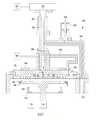
圖1係根據本案揭露之一些實施例的基板處理腔室(處理腔室100)之概略視圖,該處理腔室包含適合用於ALD製程的氣體輸送系統130。圖2係該處理腔室100之概略剖面視圖。處理腔室100包含腔室主體102,該腔室主體102具有在該腔室主體102內且在該腔室蓋組件132下方之處理空間。該處理腔室100之狹縫閥108提供機器人(圖中未顯示)進出途徑(access),以將基板110傳送到該處理腔室100以及從該處理腔室100收回基板110,所述基板110比如為200 mm或300 mm之半導體晶圓或玻璃基板。腔室襯墊177係沿著該處理腔室100之牆面以配置,以保護該腔室隔絕在處理/清洗期間使用之腐蝕性氣體。FIG. 1 is a schematic view of a substrate processing chamber (processing chamber 100) according to some embodiments disclosed in the present application. The processing chamber includes a
基板支撐件112將該基板110支撐在該處理腔室100中的基板接受表面111上。該基板支撐件112係架設於升舉馬達114以升起與下降該基板支撐件112與配置於該基板支撐件上之該基板110。升舉板116(如圖2所示)連接至升舉馬達118,該升舉板116係架設在該處理腔室100中以升起與下降升舉銷120,該等升舉銷可動式配置成穿過該基板支撐件112。該等升舉銷120在該基板支撐件112表面之上方升起與下降該基板110。該基板支撐件112可包含真空卡盤(圖中未顯示)、靜電卡盤(圖中未顯示)、夾環(圖中未顯示)以在沉積製程中將該基板110固定至該基板支撐件112。The
該基板支撐件112之溫度可被調整以控制該基板110之溫度。例如,基板支撐件112可用內嵌之加熱元件來加熱,所述內嵌之加熱元件比如電阻加熱器(圖中未顯示),或者是基板支撐件112可使用輻射熱來加熱,所述輻射熱比如配置於該基板支撐件112之上之加熱燈(圖中未顯示)。淨化環122可配置於該基板支撐件112上以界定淨化通道124,該淨化通道提供淨化氣體至該基板110之周邊部以防止該基板110之周邊部上的沉積。The temperature of the
氣體輸送系統130係被配置於該腔室主體102之上部以提供氣體至處理腔室100,所述氣體比如處理氣體與/或淨化氣體。真空系統(圖中未顯示)係與泵送通道179連通以從該處理腔室100排空任何所欲之氣體並且幫助維持在該處理腔室100內之所欲氣壓或氣壓範圍。The
在一些實施例中,該腔室蓋組件132包含氣體分散通道134,該氣體分散通道延伸通過該腔室蓋組件132之中央部。如圖式1與2所示,該氣體分散通道134向該基板接受表面111垂直延伸並且也沿著該氣體分散通道134之中央軸133延伸,通過蓋板170、至下表面160。在一些實施例中,該氣體分散通道134之上部係實質地沿著中央軸133呈圓柱形,並且該氣體分散通道134之下部漸縮(taper)遠離中央軸133。該下表面160之尺寸與構形設計成實質地覆蓋該基板110,該基板110配置於該基板支撐件112之該基板接受表面111上。該下表面160從該蓋板170之外邊緣朝向該氣體分散通道134漸縮。該氣體輸送系統130可提供一或多種氣體至該氣體分散通道134以處理該基板110。在一些實施例中,氣體輸送系統130可以經由一個氣體入口耦合於該氣體分散通道134。在一些實施例中,比如如圖3所示者,該氣體輸送系統可以經由複數個入口耦合於該氣體分散通道134。In some embodiments, the
如圖3所說明者,環形氣流174說明通過該氣體分散通道134之該處理氣體之流動,該環形氣流174可含有各種類型的流動形態(flow pattern)。在一些實施例中,當處理氣體通過該分散通道時,可以迫使處理氣體繞著氣體分散通道134之中央軸133周圍迴轉(revolution)。在此實施例中,該環形氣流174可含有各種環形流動形態,比如渦流形態、螺旋(helix)形態、繞軸(spiral)形態、或前述形態之衍生形態。As illustrated in FIG. 3, the
雖然提供環形氣流174係對於眾多應用為有利的,發明人已發現在一些應用中,該環形氣流能引起非均勻處理之結果。發明人已觀察到該氣流在靠近正受處理之該基板110之中心可引起甜甜圈形沉積分佈曲線。該甜甜圈形型態可能是由該氣體分散通道134之漏斗狀所導致。因此,在一些實施例中,該處理腔室100進一步包含氣體分配板125,該氣體分配板具有複數個縫隙126,該等縫隙126配置成穿過該氣體分配板125。該氣體分配板125延伸至該氣體分散通道134之表面,以使得僅有從該氣體分散通道134至該基板之路徑係經該氣體分配板125之複數個縫隙126。該氣體分配板125有利地創造通過該氣體分配板125之氣體之扼流,造成基板110上有更均勻之沉積,並且因此實質地消除由該氣體之轉動流所導致之該甜甜圈形沉積。Although the provision of
在一些實施例中,該氣體分配板125係由非腐蝕性陶瓷材料形成,比如,例如鋁氧化物或鋁氮化物。在一些實施例中,該複數個縫隙126之各者可具有相等的流體傳導率。在一些實施例中,該複數個縫隙126之密度(比如,每單位面積之縫隙數量或縫隙開口之尺寸)可遍及該氣體分配板125變化以在該基板110上達成所欲之沉積型態。例如,可於氣體分配板125之中心配置較高密度的縫隙126,以增加相對於該基板邊緣的在基板中心之沉積速率,而進一步改善沉積均勻度。In some embodiments, the
雖然該複數個縫隙126係被描述為圓柱狀通孔,但該複數個縫隙126可具有不同之輪廓。圖式4A至圖4C描述複數個縫隙126的輪廓的不同、非限制性實施例。於圖4A描述之實施例中,該縫隙126係圓柱狀通孔,該圓柱狀通孔具有環繞於該縫隙的彎曲邊緣402。於圖4B描述之該實施例中,該縫隙126係通孔,該通孔具有向內朝該縫隙中心漸縮之上部404、垂直延伸至氣體分配板125上表面127之圓柱中央部405、以及從該縫隙中心向外漸縮之下部406。於圖4C描述之該實施例中,該縫隙126係通孔,該通孔具有上部408,垂直延伸至氣體分配板125上表面127之圓柱中央部409、以及從該縫隙中心向外漸縮之下部410,而該上部408具有錐坑孔(countersunk hole)。可取而代之使用複數個縫隙126之其他輪廓,以在該基板110處理期間達成最佳沉積均勻度。Although the plurality of
不希望被理論所囿,發明人相信氣體分散通道134之直徑(所述直徑從氣體分散通道134之上部至沿著中央軸133之第一點為定值,並且該直徑從該第一點至氣體分散通道134之下部135增加)允許較少的通過氣體分散通道134的氣體絕熱膨脹,而幫助控制該環形氣流174中所含的處理氣體之溫度。例如,輸送進入氣體分散通道134之氣體的突然絕熱膨脹可能造成該氣體溫度下墜,而可能導致該氣體冷凝與形成液滴。另一方面,相信逐漸地漸縮的氣體分散通道134提供較少之氣體絕熱膨脹。因此,更多的熱可傳遞至該氣體或從該氣體傳遞,並且因此該氣體之溫度可以更簡單地藉由控制該腔室蓋組件132之溫度而控制。氣體分散通道134可逐漸地漸縮並且含有一或多個漸縮之內表面,比如漸縮筆直表面、內凹表面、外凸表面或上述表面之組合,或可含有一或多個漸縮之內表面的分段(亦即,部分漸縮與部分未漸縮)。Without wishing to be bound by theory, the inventor believes that the diameter of the gas dispersion channel 134 (the diameter from the upper part of the
如圖3所示,氣體分散通道134之上部係以配置於外殼375之內區域中之插入件300界定。該插入件300包含位在插入件300之上部的帽302與至少部分界定該氣體分散通道134之中央通路。該帽302延伸過該外殼375以固著該插入件300到位。該插入件300與帽302包含複數個O形環385,該O形環配置於該插入件300與該外殼375之間,以確保適當密封。該插入件300包含複數個周圍縫隙,當該插入件300插入外殼375時,該周圍縫隙形成相對應之複數個周圍通道360、365、370。該複數個周圍通道360、365、370係經由相對應之複數個孔 340、345、350流體連通式耦合於該氣體分散通道134。在圖3所示之實施例中,該氣體輸送系統130係經由複數個氣體饋送線路310、315、320耦合於該氣體分散通道134。該氣體饋送線路310、315、320係流體連通式耦合於該複數個周圍通道360、365、370以提供一或多種氣體至該氣體分散通道134。As shown in FIG. 3, the upper portion of the
回到圖1與圖2,該處理腔室100進一步包含腔室清洗系統,該腔室清洗系統包含遠端電漿源(RPS)190、於一端耦合該RPS 190並於相對端耦合該帽302的隔離套環192、耦合於蓋板170上表面之加熱板198、以及流體連通式耦合於該RPS 190之清洗氣體(亦即,淨化氣體)之氣源197。該清洗氣源可包含任合適合形成電漿以清洗處理腔室100的氣體。在一些實施例中,例如,該清洗氣體可以為三氟化氮(NF3)。該隔離套環192包含內通道193,該內通道193透過配置於帽302中央部之複數個孔285流體連通式耦合於該氣體分散通道134,以使電漿從該RPS 190流動通過該氣體分散通道134且流入該反應區164。該加熱板198可以由不銹鋼形成並且包含複數個耐熱元件,該等耐熱元件分散在該板各處。Returning to FIGS. 1 and 2, the
典型地,在氣體輸送系統130提供第一氣體至氣體分散通道134之後,清洗氣體流動通過該氣體分散通道134與反應區164,以快速地從氣體分散通道134與反應區164淨化第一氣體。之後,由氣體輸送系統130提供第二氣體至氣體分散通道134,並且該清洗氣體再一次地流動通過氣體分散通道134而至反應區164,以快速地從氣體分散通道134與反應區164淨化第二氣體。然而,添加氣體分配板125會堵塞(choke)該清洗氣體至泵送通道179之流動,並且延長了清洗製程。就此而言,發明人已併入排氣系統180,該排氣系統180具有排氣導管184,該排氣導管184在第一端186耦合隔離套環192,並且在第二端188耦合泵送通道179。閥182係配置於排氣導管184中,以選擇性地將排氣導管184流體連通式耦合至內通道193。在一些實施例中,例如,該閥182可以為具有柱塞202的柱塞形式閥,該柱塞202可在第一位置(如圖2所示)與第二位置之間移動,該柱塞202在該第一位置將排氣導管184流體連通式耦合至內通道193,而該柱塞202在該第二位置使排氣導管184密封隔絕該內通道193。每一次當清洗氣流動通過該氣體分散通道134與該反應區164,該閥182開啟並且該清洗氣體快速地排出至泵送通道179。Typically, after the
當處理腔室100之內側氣壓超過於該RPS 190內側之氣壓時,處理氣體可向上流至該RPS 190並損壞該RPS 190。該複數個孔285係用於作為扼流點以防止處理氣體之逆流向上流動通過內通道193並且進入該RPS 190中。該隔離套環192可由任何對所用之清洗氣體不反應之材料所形成。在一些實施例中,當該清洗氣體係NF3時,該隔離套環192可為鋁所形成。在一些實施例中,隔離套環192與插入件300可由鋁所形成並且鍍上塗層以防止隔離套環192與插入件300因所使用之腐蝕性氣體之腐蝕。例如,該塗層可以鎳或鋁氧化物形成。When the pressure inside the
參照圖3,RPS 190在小於或等於約40°C之溫度下運作。為求有利地使RPS 190隔絕處理腔室100中所產生之熱,絕熱環394係配置於該隔離套環192與帽302之間。該絕熱環394係由具低熱導率之金屬形成(例如,低於隔離套環192與帽302之熱導率)。還有,O形環385也可配置於隔離套環192與帽302之間以進一步減低隔離套環192與帽302之間之接觸面積。絕熱環394與O形環385之組合扮演熱的扼流(thermal choke)以確保在處理腔室100中產生之熱不會負面地影響該RPS 190。Referring to Figure 3, the
在一些實施例中,當蓋板170被加熱過100°C時,該處理腔室100可包含差動泵送線路250以確保任何陷於O形環385之間的處理氣體或副產物排出至該泵送通道179。該差動泵送線路250於第一端耦合蓋板170且於第二端耦合外殼375,該第二端與該第一端相對。該差動泵送線路係流體連通式耦合於氣體分散通道134與一或更多個通道260,該通道260在二個或更多個O形環385之間的區域形成。當該閥182係開啟以使氣體分散通道134排氣時,該差動泵送線路排出被陷於O形環385之間之氣體。In some embodiments, when the
回到圖3,腔室蓋組件132之下表面160之一部分可從耦合氣體分散通道134的中央開口至腔室蓋組件132之周邊部向下與向外呈一輪廓或呈一角度,以幫助來自氣體分散通道134在橫跨該基板110之表面(亦即,從該基板之中心至該基板之邊緣)上有改善的速率分佈曲線(velocity profile)。下表面160可含有一或更多個表面,比如筆直表面、外凸表面、內凹表面或上述表面之組合。在一個範例中,下表面160係外凸呈漏斗狀。Returning to FIG. 3, a part of the
在一個範例中,下表面160係朝基板接受表面111之邊緣向下向外傾斜,以助於使在腔室蓋組件132之下表面160與基板110之間行進的處理氣體的速率變化減少,同時協助該基板110之表面均勻地暴露至反應物氣體。腔室蓋組件132之部件與零件可含有材料,比如不銹鋼、鋁、鍍鎳鋁、鎳、上述材料之合金、或其他合適之材料。在一個實施例中,蓋板170可從金屬獨立地建造、機械加工(machine)、鍛造、或其他方式製作,所述金屬比如鋁、鋁合金、鋼、不鏽鋼、上述金屬之合金、或上述金屬之組合。In one example, the
在一些實施例中,氣體分散通道134之內表面131與腔室蓋組件132之下表面160可含有鏡面拋光面以幫助氣體沿著氣體分散通道134與腔室蓋組件132之下表面160流動。In some embodiments, the inner surface 131 of the
參照圖1至圖3,在處理運作中,基板110係藉由機器人(圖中未顯示)經狹縫閥108輸送至處理腔室100。基板110係透過升舉銷120與該機器人之合作而定位在基板支撐件112上。基板支撐件112升起基板110至與該氣體分配板125之下表面相對且接近之位置(close opposition)。第一氣流可藉由氣體輸送系統130注入處理腔室100之氣體分散通道134,該第一氣流之注入是與第二氣流一起或分開(亦即,脈衝)。該第一氣流可含有來自淨化氣源的連續的淨化氣體之連續流以及來自反應物氣源的反應物氣體之脈衝,或可含有來自反應物氣源的反應物氣體之脈衝以及來自淨化氣源的淨化氣體之脈衝。該第二氣流可含有來自淨化氣源的淨化氣流之連續流以及來自反應物氣源的反應物氣體之脈衝,或可含有來自反應物氣源的反應物氣體之脈衝以及來自淨化氣源的淨化氣體之脈衝。1 to 3, in the processing operation, the
該環形氣流174行進通過氣體分散通道134並且之後通過氣體分配板125中之該複數個縫隙126。然後該氣體沉積在基板110之表面上。腔室蓋組件132之下表面160係向下傾斜,該腔室蓋組件132之下表面160幫助減低遍及氣體分配板125之表面上的氣流之速率變化。過多氣體、副產物等流入該泵送通道179,然後從處理腔室100排出。在整個處理運作中,該加熱板198可加熱該腔室蓋組件132至預定溫度,以加熱已累積在該處理腔室100牆面(或配置在該腔室之處理套件)上的任何固體副產物。結果為,任何累積的固體副產物皆被汽化。該汽化之副產物被真空系統(未顯示)與泵送通道179抽空。在一些實施例中,預定溫度係大於或等於150 °C。The
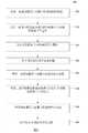
圖5說明根據本案揭露之一些實施例之處理基板之方法500。於步驟505,使第一處理氣體從氣體輸送系統130流入氣體分散通道134與反應區164中。於步驟510,該第一處理氣體流動通過該氣體分配板125中之複數個縫隙126,並且流至基板110上。於步驟515,清洗氣體係流入該氣體分散通道134與該反應區164,以淨化該第一處理氣體。於步驟520,該清洗氣體係經由該排氣系統180排出。於步驟525,第二處理氣體流入氣體分散通道134與反應區164。於步驟530,該第二處理氣體流動通過該氣體分配板125中之複數個縫隙126,並且流至基板110上。於步驟535,該清洗氣體流入該氣體分散通道134與該反應區164,以淨化該第二處理氣體。於步驟540,該清洗氣體係經由該排氣系統180排出。FIG. 5 illustrates a
其他適用於原子層沉積之腔室之實施例併有一或多個此等特徵。Other embodiments of chambers suitable for atomic layer deposition do not have one or more of these features.
雖然上述內容述係針對本案揭露之一些實施例,但可不脫離本案揭露之實施例的基本範疇而設計其他與進一步之實施例。Although the above description is directed to some embodiments disclosed in this case, other and further embodiments can be designed without departing from the basic scope of the embodiments disclosed in this case.
100:處理腔室102:腔室主體108:狹縫閥110:基板111:基板接受表面112:基板支撐件114:升舉馬達116:升舉板118:升舉馬達120:升舉銷122:淨化環124:淨化通道125:氣體分配板126:縫隙127:上表面130:氣體輸送系統132:腔室蓋組件133:中央軸134:氣體分散通道135:下部160:下表面164:反應區170:蓋板174:氣流177:腔室襯墊179:泵送通道180:排氣系統182:閥184:排氣導管186:第一端188:第二端190:遠端電漿源(RPS)192:隔離套環193:內通道197:清洗氣源198:加熱板202:柱塞250:差動泵送線路260:通道285:孔300:插入件302:帽310:氣體饋送線路315:氣體饋送線路320:氣體饋送線路340:孔345:孔350:孔360:周圍通道365:周圍通道370:周圍通道375:外殼385:O形環394:絕熱環402:彎曲邊緣404:上部405:圓柱中央部406:下部408:上部409:圓柱中央部410:下部500:方法505:步驟510:步驟515:步驟520:步驟525:步驟530:步驟535:步驟540:步驟100: processing chamber102: Chamber body108: slit valve110: substrate111: substrate receiving surface112: substrate support114: Lift Motor116: Lift Board118: Lift motor120: lift pin122: Purification Ring124: Purification Channel125: Gas distribution plate126: Gap127: upper surface130: Gas delivery system132: Chamber cover assembly133: Central axis134: Gas dispersion channel135: Lower160: lower surface164: reaction zone170: cover174: Airflow177: Chamber Liner179: Pumping channel180: exhaust system182: Valve184: Exhaust duct186: The first end188: second end190: Remote Plasma Source (RPS)192: isolation collar193: Inner Channel197: Cleaning Air Source198: heating plate202: Plunger250: Differential pumping line260: Channel285: hole300: Insert302: cap310: Gas feed line315: Gas feed line320: Gas feed line340: hole345: hole350: hole360: Surrounding channel365: Surrounding channel370: Surrounding Channel375: Shell385: O-ring394: Adiabatic Ring402: curved edge404: Upper405: Central part of column406: Lower408: Upper409: central part of column410: Lower500: method505: step510: Step515: step520: step525: step530: step535: step540: step
透過參考附圖所繪的本案揭露之說明性實施例,能理解上文簡要概述且於下文更詳細討論的本案揭露之實施例。然而,該附圖僅說明本案揭露之典型實施例,因此不被認為是限制範疇,因為本案揭露內容可容認其他等效實施例。The illustrative embodiments of the present disclosure, which are briefly summarized above and discussed in more detail below, can be understood through the illustrative embodiments of the present disclosure drawn with reference to the accompanying drawings. However, the drawings only illustrate the typical embodiments disclosed in this case, and therefore are not considered to be a limiting category, because the contents disclosed in this case can recognize other equivalent embodiments.
圖1描述根據本案揭露之一些實施例之處理腔室概略視圖。Figure 1 depicts a schematic view of a processing chamber according to some embodiments disclosed in the present application.
圖2描述根據本案揭露之一些實施例之處理腔室的概略剖面視圖。Figure 2 depicts a schematic cross-sectional view of a processing chamber according to some embodiments disclosed in the present application.
圖3描述根據本案揭露之一些實施例之蓋組件的概略剖面視圖。FIG. 3 depicts a schematic cross-sectional view of a cover assembly according to some embodiments disclosed in this application.
圖4A至圖4C描述根據本案揭露之一些實施例之配置成穿過氣體分配板的縫隙的概略視圖圖。4A to 4C depict schematic views of some embodiments according to the present disclosure configured to pass through the gap of the gas distribution plate.
圖5描述流程圖,說明根據本案揭露之實施例之處理基板方法。FIG. 5 depicts a flowchart illustrating a method of processing a substrate according to an embodiment disclosed in this application.
為幫助理解,如可能則已使用相同的元件符號指定該等圖式共通的相同元件。該等圖式不按比例繪製並且為了清楚起見可被簡化。一個實施例之元件與特徵可被有益地併入其他實施例而無需另外記載。To aid understanding, the same component symbols have been used to designate the same components common to the drawings if possible. The diagrams are not drawn to scale and may be simplified for clarity. The elements and features of one embodiment can be beneficially incorporated into other embodiments without additional description.
國內寄存資訊(請依寄存機構、日期、號碼順序註記)無國外寄存資訊(請依寄存國家、機構、日期、號碼順序註記)無Domestic deposit information (please note in the order of deposit institution, date and number)noForeign hosting information (please note in the order of hosting country, institution, date and number)no
114:升舉馬達114: Lift Motor
116:升舉板116: Lift Board
118:升舉馬達118: Lift motor
120:升舉銷120: lift pin
122:淨化環122: Purification Ring
124:淨化通道124: Purification Channel
125:氣體分配板125: Gas distribution plate
126:縫隙126: Gap
130:氣體輸送系統130: Gas delivery system
134:氣體分散通道134: Gas dispersion channel
135:下部135: Lower
160:下表面160: lower surface
164反應區164 reaction zone
170:蓋板170: cover
179:泵送通道179: Pumping channel
180:排氣系統180: exhaust system
182:閥182: Valve
184:排氣導管184: Exhaust duct
190:遠端電漿源(RPS)190: Remote Plasma Source (RPS)
192:隔離套環192: isolation collar
193:內通道193: Inner Channel
197:清洗氣源197: Cleaning Air Source
198:加熱板198: heating plate
202:柱塞202: Plunger
250:差動泵送線路250: Differential pumping line
260:通道260: Channel
285:孔285: hole
Claims (20)
Translated fromChineseApplications Claiming Priority (4)
| Application Number | Priority Date | Filing Date | Title |
|---|---|---|---|
| US201562151180P | 2015-04-22 | 2015-04-22 | |
| US62/151,180 | 2015-04-22 | ||
| US14/734,838US11384432B2 (en) | 2015-04-22 | 2015-06-09 | Atomic layer deposition chamber with funnel-shaped gas dispersion channel and gas distribution plate |
| US14/734,838 | 2015-06-09 |
Publications (2)
| Publication Number | Publication Date |
|---|---|
| TW202028525Atrue TW202028525A (en) | 2020-08-01 |
| TWI722871B TWI722871B (en) | 2021-03-21 |
Family
ID=57144181
Family Applications (2)
| Application Number | Title | Priority Date | Filing Date |
|---|---|---|---|
| TW109112814ATWI722871B (en) | 2015-04-22 | 2016-04-18 | Lid and lid assembly kit for substrate processing chamber |
| TW105112023ATWI693298B (en) | 2015-04-22 | 2016-04-18 | Atomic layer deposition chamber with funnel-shaped gas dispersion channel and gas distribution plate |
Family Applications After (1)
| Application Number | Title | Priority Date | Filing Date |
|---|---|---|---|
| TW105112023ATWI693298B (en) | 2015-04-22 | 2016-04-18 | Atomic layer deposition chamber with funnel-shaped gas dispersion channel and gas distribution plate |
Country Status (8)
| Country | Link |
|---|---|
| US (2) | US11384432B2 (en) |
| EP (1) | EP3286352B1 (en) |
| KR (2) | KR102631744B1 (en) |
| CN (2) | CN112877675B (en) |
| IL (2) | IL284142B2 (en) |
| SG (2) | SG10202111772XA (en) |
| TW (2) | TWI722871B (en) |
| WO (1) | WO2016172085A1 (en) |
Families Citing this family (385)
| Publication number | Priority date | Publication date | Assignee | Title |
|---|---|---|---|---|
| US10378106B2 (en) | 2008-11-14 | 2019-08-13 | Asm Ip Holding B.V. | Method of forming insulation film by modified PEALD |
| US9394608B2 (en) | 2009-04-06 | 2016-07-19 | Asm America, Inc. | Semiconductor processing reactor and components thereof |
| US8802201B2 (en) | 2009-08-14 | 2014-08-12 | Asm America, Inc. | Systems and methods for thin-film deposition of metal oxides using excited nitrogen-oxygen species |
| US9312155B2 (en) | 2011-06-06 | 2016-04-12 | Asm Japan K.K. | High-throughput semiconductor-processing apparatus equipped with multiple dual-chamber modules |
| US10364496B2 (en) | 2011-06-27 | 2019-07-30 | Asm Ip Holding B.V. | Dual section module having shared and unshared mass flow controllers |
| US10854498B2 (en) | 2011-07-15 | 2020-12-01 | Asm Ip Holding B.V. | Wafer-supporting device and method for producing same |
| US20130023129A1 (en) | 2011-07-20 | 2013-01-24 | Asm America, Inc. | Pressure transmitter for a semiconductor processing environment |
| US9017481B1 (en) | 2011-10-28 | 2015-04-28 | Asm America, Inc. | Process feed management for semiconductor substrate processing |
| US9659799B2 (en) | 2012-08-28 | 2017-05-23 | Asm Ip Holding B.V. | Systems and methods for dynamic semiconductor process scheduling |
| US10714315B2 (en) | 2012-10-12 | 2020-07-14 | Asm Ip Holdings B.V. | Semiconductor reaction chamber showerhead |
| US20160376700A1 (en) | 2013-02-01 | 2016-12-29 | Asm Ip Holding B.V. | System for treatment of deposition reactor |
| US9484191B2 (en) | 2013-03-08 | 2016-11-01 | Asm Ip Holding B.V. | Pulsed remote plasma method and system |
| US9589770B2 (en) | 2013-03-08 | 2017-03-07 | Asm Ip Holding B.V. | Method and systems for in-situ formation of intermediate reactive species |
| US9240412B2 (en) | 2013-09-27 | 2016-01-19 | Asm Ip Holding B.V. | Semiconductor structure and device and methods of forming same using selective epitaxial process |
| US10683571B2 (en) | 2014-02-25 | 2020-06-16 | Asm Ip Holding B.V. | Gas supply manifold and method of supplying gases to chamber using same |
| US10167557B2 (en) | 2014-03-18 | 2019-01-01 | Asm Ip Holding B.V. | Gas distribution system, reactor including the system, and methods of using the same |
| US11015245B2 (en) | 2014-03-19 | 2021-05-25 | Asm Ip Holding B.V. | Gas-phase reactor and system having exhaust plenum and components thereof |
| US10858737B2 (en) | 2014-07-28 | 2020-12-08 | Asm Ip Holding B.V. | Showerhead assembly and components thereof |
| US9890456B2 (en) | 2014-08-21 | 2018-02-13 | Asm Ip Holding B.V. | Method and system for in situ formation of gas-phase compounds |
| US9793096B2 (en)* | 2014-09-12 | 2017-10-17 | Lam Research Corporation | Systems and methods for suppressing parasitic plasma and reducing within-wafer non-uniformity |
| US10407771B2 (en)* | 2014-10-06 | 2019-09-10 | Applied Materials, Inc. | Atomic layer deposition chamber with thermal lid |
| US9657845B2 (en) | 2014-10-07 | 2017-05-23 | Asm Ip Holding B.V. | Variable conductance gas distribution apparatus and method |
| US10941490B2 (en) | 2014-10-07 | 2021-03-09 | Asm Ip Holding B.V. | Multiple temperature range susceptor, assembly, reactor and system including the susceptor, and methods of using the same |
| KR102263121B1 (en) | 2014-12-22 | 2021-06-09 | 에이에스엠 아이피 홀딩 비.브이. | Semiconductor device and manufacuring method thereof |
| US10529542B2 (en) | 2015-03-11 | 2020-01-07 | Asm Ip Holdings B.V. | Cross-flow reactor and method |
| US10276355B2 (en) | 2015-03-12 | 2019-04-30 | Asm Ip Holding B.V. | Multi-zone reactor, system including the reactor, and method of using the same |
| US11384432B2 (en)* | 2015-04-22 | 2022-07-12 | Applied Materials, Inc. | Atomic layer deposition chamber with funnel-shaped gas dispersion channel and gas distribution plate |
| KR101792941B1 (en)* | 2015-04-30 | 2017-11-02 | 어드밴스드 마이크로 패브리케이션 이큅먼트 인코퍼레이티드, 상하이 | A Chemical Vapor Deposition Apparatus and Its Cleaning Method |
| US10458018B2 (en) | 2015-06-26 | 2019-10-29 | Asm Ip Holding B.V. | Structures including metal carbide material, devices including the structures, and methods of forming same |
| US10600673B2 (en) | 2015-07-07 | 2020-03-24 | Asm Ip Holding B.V. | Magnetic susceptor to baseplate seal |
| US9960072B2 (en) | 2015-09-29 | 2018-05-01 | Asm Ip Holding B.V. | Variable adjustment for precise matching of multiple chamber cavity housings |
| US10211308B2 (en) | 2015-10-21 | 2019-02-19 | Asm Ip Holding B.V. | NbMC layers |
| US10322384B2 (en) | 2015-11-09 | 2019-06-18 | Asm Ip Holding B.V. | Counter flow mixer for process chamber |
| US11139308B2 (en) | 2015-12-29 | 2021-10-05 | Asm Ip Holding B.V. | Atomic layer deposition of III-V compounds to form V-NAND devices |
| US10468251B2 (en) | 2016-02-19 | 2019-11-05 | Asm Ip Holding B.V. | Method for forming spacers using silicon nitride film for spacer-defined multiple patterning |
| US10529554B2 (en) | 2016-02-19 | 2020-01-07 | Asm Ip Holding B.V. | Method for forming silicon nitride film selectively on sidewalls or flat surfaces of trenches |
| US10501866B2 (en) | 2016-03-09 | 2019-12-10 | Asm Ip Holding B.V. | Gas distribution apparatus for improved film uniformity in an epitaxial system |
| US10343920B2 (en) | 2016-03-18 | 2019-07-09 | Asm Ip Holding B.V. | Aligned carbon nanotubes |
| US9892913B2 (en) | 2016-03-24 | 2018-02-13 | Asm Ip Holding B.V. | Radial and thickness control via biased multi-port injection settings |
| US10190213B2 (en) | 2016-04-21 | 2019-01-29 | Asm Ip Holding B.V. | Deposition of metal borides |
| US10865475B2 (en) | 2016-04-21 | 2020-12-15 | Asm Ip Holding B.V. | Deposition of metal borides and silicides |
| US10367080B2 (en) | 2016-05-02 | 2019-07-30 | Asm Ip Holding B.V. | Method of forming a germanium oxynitride film |
| US10032628B2 (en) | 2016-05-02 | 2018-07-24 | Asm Ip Holding B.V. | Source/drain performance through conformal solid state doping |
| KR102592471B1 (en) | 2016-05-17 | 2023-10-20 | 에이에스엠 아이피 홀딩 비.브이. | Method of forming metal interconnection and method of fabricating semiconductor device using the same |
| US11453943B2 (en) | 2016-05-25 | 2022-09-27 | Asm Ip Holding B.V. | Method for forming carbon-containing silicon/metal oxide or nitride film by ALD using silicon precursor and hydrocarbon precursor |
| KR102102320B1 (en)* | 2016-06-28 | 2020-04-22 | 주식회사 원익아이피에스 | Wafer Processing Apparatus And Method of depositing Thin film Using The Same |
| US10388509B2 (en) | 2016-06-28 | 2019-08-20 | Asm Ip Holding B.V. | Formation of epitaxial layers via dislocation filtering |
| US9859151B1 (en) | 2016-07-08 | 2018-01-02 | Asm Ip Holding B.V. | Selective film deposition method to form air gaps |
| US10612137B2 (en) | 2016-07-08 | 2020-04-07 | Asm Ip Holdings B.V. | Organic reactants for atomic layer deposition |
| US10714385B2 (en) | 2016-07-19 | 2020-07-14 | Asm Ip Holding B.V. | Selective deposition of tungsten |
| KR102354490B1 (en) | 2016-07-27 | 2022-01-21 | 에이에스엠 아이피 홀딩 비.브이. | Method of processing a substrate |
| US10395919B2 (en) | 2016-07-28 | 2019-08-27 | Asm Ip Holding B.V. | Method and apparatus for filling a gap |
| US9812320B1 (en) | 2016-07-28 | 2017-11-07 | Asm Ip Holding B.V. | Method and apparatus for filling a gap |
| US9887082B1 (en) | 2016-07-28 | 2018-02-06 | Asm Ip Holding B.V. | Method and apparatus for filling a gap |
| KR102532607B1 (en) | 2016-07-28 | 2023-05-15 | 에이에스엠 아이피 홀딩 비.브이. | Substrate processing apparatus and method of operating the same |
| KR102613349B1 (en) | 2016-08-25 | 2023-12-14 | 에이에스엠 아이피 홀딩 비.브이. | Exhaust apparatus and substrate processing apparatus and thin film fabricating method using the same |
| US10410943B2 (en) | 2016-10-13 | 2019-09-10 | Asm Ip Holding B.V. | Method for passivating a surface of a semiconductor and related systems |
| US10643826B2 (en) | 2016-10-26 | 2020-05-05 | Asm Ip Holdings B.V. | Methods for thermally calibrating reaction chambers |
| US11532757B2 (en) | 2016-10-27 | 2022-12-20 | Asm Ip Holding B.V. | Deposition of charge trapping layers |
| US10643904B2 (en) | 2016-11-01 | 2020-05-05 | Asm Ip Holdings B.V. | Methods for forming a semiconductor device and related semiconductor device structures |
| US10229833B2 (en) | 2016-11-01 | 2019-03-12 | Asm Ip Holding B.V. | Methods for forming a transition metal nitride film on a substrate by atomic layer deposition and related semiconductor device structures |
| US10435790B2 (en) | 2016-11-01 | 2019-10-08 | Asm Ip Holding B.V. | Method of subatmospheric plasma-enhanced ALD using capacitively coupled electrodes with narrow gap |
| US10714350B2 (en) | 2016-11-01 | 2020-07-14 | ASM IP Holdings, B.V. | Methods for forming a transition metal niobium nitride film on a substrate by atomic layer deposition and related semiconductor device structures |
| US10134757B2 (en) | 2016-11-07 | 2018-11-20 | Asm Ip Holding B.V. | Method of processing a substrate and a device manufactured by using the method |
| KR102546317B1 (en) | 2016-11-15 | 2023-06-21 | 에이에스엠 아이피 홀딩 비.브이. | Gas supply unit and substrate processing apparatus including the same |
| US10340135B2 (en) | 2016-11-28 | 2019-07-02 | Asm Ip Holding B.V. | Method of topologically restricted plasma-enhanced cyclic deposition of silicon or metal nitride |
| KR102762543B1 (en) | 2016-12-14 | 2025-02-05 | 에이에스엠 아이피 홀딩 비.브이. | Substrate processing apparatus |
| US11447861B2 (en) | 2016-12-15 | 2022-09-20 | Asm Ip Holding B.V. | Sequential infiltration synthesis apparatus and a method of forming a patterned structure |
| US11581186B2 (en) | 2016-12-15 | 2023-02-14 | Asm Ip Holding B.V. | Sequential infiltration synthesis apparatus |
| KR102700194B1 (en) | 2016-12-19 | 2024-08-28 | 에이에스엠 아이피 홀딩 비.브이. | Substrate processing apparatus |
| US10269558B2 (en) | 2016-12-22 | 2019-04-23 | Asm Ip Holding B.V. | Method of forming a structure on a substrate |
| US10867788B2 (en) | 2016-12-28 | 2020-12-15 | Asm Ip Holding B.V. | Method of forming a structure on a substrate |
| US11390950B2 (en) | 2017-01-10 | 2022-07-19 | Asm Ip Holding B.V. | Reactor system and method to reduce residue buildup during a film deposition process |
| EP3568504A4 (en)* | 2017-01-16 | 2021-01-06 | Sustainable Energy Solutions, LLC | Method and apparatus for desublimation prevention in a direct contact heat exchanger |
| US10655221B2 (en) | 2017-02-09 | 2020-05-19 | Asm Ip Holding B.V. | Method for depositing oxide film by thermal ALD and PEALD |
| US10468261B2 (en) | 2017-02-15 | 2019-11-05 | Asm Ip Holding B.V. | Methods for forming a metallic film on a substrate by cyclical deposition and related semiconductor device structures |
| US9972501B1 (en)* | 2017-03-14 | 2018-05-15 | Nano-Master, Inc. | Techniques and systems for continuous-flow plasma enhanced atomic layer deposition (PEALD) |
| US10529563B2 (en) | 2017-03-29 | 2020-01-07 | Asm Ip Holdings B.V. | Method for forming doped metal oxide films on a substrate by cyclical deposition and related semiconductor device structures |
| US10283353B2 (en) | 2017-03-29 | 2019-05-07 | Asm Ip Holding B.V. | Method of reforming insulating film deposited on substrate with recess pattern |
| KR102457289B1 (en) | 2017-04-25 | 2022-10-21 | 에이에스엠 아이피 홀딩 비.브이. | Method for depositing a thin film and manufacturing a semiconductor device |
| US10770286B2 (en) | 2017-05-08 | 2020-09-08 | Asm Ip Holdings B.V. | Methods for selectively forming a silicon nitride film on a substrate and related semiconductor device structures |
| US10892156B2 (en) | 2017-05-08 | 2021-01-12 | Asm Ip Holding B.V. | Methods for forming a silicon nitride film on a substrate and related semiconductor device structures |
| US10446393B2 (en) | 2017-05-08 | 2019-10-15 | Asm Ip Holding B.V. | Methods for forming silicon-containing epitaxial layers and related semiconductor device structures |
| US10504742B2 (en) | 2017-05-31 | 2019-12-10 | Asm Ip Holding B.V. | Method of atomic layer etching using hydrogen plasma |
| US10886123B2 (en) | 2017-06-02 | 2021-01-05 | Asm Ip Holding B.V. | Methods for forming low temperature semiconductor layers and related semiconductor device structures |
| US12040200B2 (en) | 2017-06-20 | 2024-07-16 | Asm Ip Holding B.V. | Semiconductor processing apparatus and methods for calibrating a semiconductor processing apparatus |
| US11306395B2 (en) | 2017-06-28 | 2022-04-19 | Asm Ip Holding B.V. | Methods for depositing a transition metal nitride film on a substrate by atomic layer deposition and related deposition apparatus |
| US10685834B2 (en) | 2017-07-05 | 2020-06-16 | Asm Ip Holdings B.V. | Methods for forming a silicon germanium tin layer and related semiconductor device structures |
| KR20190009245A (en) | 2017-07-18 | 2019-01-28 | 에이에스엠 아이피 홀딩 비.브이. | Methods for forming a semiconductor device structure and related semiconductor device structures |
| US11374112B2 (en) | 2017-07-19 | 2022-06-28 | Asm Ip Holding B.V. | Method for depositing a group IV semiconductor and related semiconductor device structures |
| US11018002B2 (en) | 2017-07-19 | 2021-05-25 | Asm Ip Holding B.V. | Method for selectively depositing a Group IV semiconductor and related semiconductor device structures |
| US10541333B2 (en) | 2017-07-19 | 2020-01-21 | Asm Ip Holding B.V. | Method for depositing a group IV semiconductor and related semiconductor device structures |
| US10312055B2 (en) | 2017-07-26 | 2019-06-04 | Asm Ip Holding B.V. | Method of depositing film by PEALD using negative bias |
| US10590535B2 (en) | 2017-07-26 | 2020-03-17 | Asm Ip Holdings B.V. | Chemical treatment, deposition and/or infiltration apparatus and method for using the same |
| US10605530B2 (en) | 2017-07-26 | 2020-03-31 | Asm Ip Holding B.V. | Assembly of a liner and a flange for a vertical furnace as well as the liner and the vertical furnace |
| TWI815813B (en) | 2017-08-04 | 2023-09-21 | 荷蘭商Asm智慧財產控股公司 | Showerhead assembly for distributing a gas within a reaction chamber |
| US10770336B2 (en) | 2017-08-08 | 2020-09-08 | Asm Ip Holding B.V. | Substrate lift mechanism and reactor including same |
| US10692741B2 (en) | 2017-08-08 | 2020-06-23 | Asm Ip Holdings B.V. | Radiation shield |
| US11769682B2 (en) | 2017-08-09 | 2023-09-26 | Asm Ip Holding B.V. | Storage apparatus for storing cassettes for substrates and processing apparatus equipped therewith |
| US10249524B2 (en) | 2017-08-09 | 2019-04-02 | Asm Ip Holding B.V. | Cassette holder assembly for a substrate cassette and holding member for use in such assembly |
| US11139191B2 (en) | 2017-08-09 | 2021-10-05 | Asm Ip Holding B.V. | Storage apparatus for storing cassettes for substrates and processing apparatus equipped therewith |
| US20190048467A1 (en)* | 2017-08-10 | 2019-02-14 | Applied Materials, Inc. | Showerhead and process chamber incorporating same |
| USD900036S1 (en) | 2017-08-24 | 2020-10-27 | Asm Ip Holding B.V. | Heater electrical connector and adapter |
| US11830730B2 (en) | 2017-08-29 | 2023-11-28 | Asm Ip Holding B.V. | Layer forming method and apparatus |
| US11295980B2 (en) | 2017-08-30 | 2022-04-05 | Asm Ip Holding B.V. | Methods for depositing a molybdenum metal film over a dielectric surface of a substrate by a cyclical deposition process and related semiconductor device structures |
| KR102491945B1 (en) | 2017-08-30 | 2023-01-26 | 에이에스엠 아이피 홀딩 비.브이. | Substrate processing apparatus |
| US11164737B2 (en)* | 2017-08-30 | 2021-11-02 | Applied Materials, Inc. | Integrated epitaxy and preclean system |
| US11056344B2 (en) | 2017-08-30 | 2021-07-06 | Asm Ip Holding B.V. | Layer forming method |
| KR102401446B1 (en) | 2017-08-31 | 2022-05-24 | 에이에스엠 아이피 홀딩 비.브이. | Substrate processing apparatus |
| US10147597B1 (en) | 2017-09-14 | 2018-12-04 | Lam Research Corporation | Turbulent flow spiral multi-zone precursor vaporizer |
| US10607895B2 (en) | 2017-09-18 | 2020-03-31 | Asm Ip Holdings B.V. | Method for forming a semiconductor device structure comprising a gate fill metal |
| KR102630301B1 (en) | 2017-09-21 | 2024-01-29 | 에이에스엠 아이피 홀딩 비.브이. | Method of sequential infiltration synthesis treatment of infiltrateable material and structures and devices formed using same |
| US10844484B2 (en) | 2017-09-22 | 2020-11-24 | Asm Ip Holding B.V. | Apparatus for dispensing a vapor phase reactant to a reaction chamber and related methods |
| US10658205B2 (en) | 2017-09-28 | 2020-05-19 | Asm Ip Holdings B.V. | Chemical dispensing apparatus and methods for dispensing a chemical to a reaction chamber |
| US10403504B2 (en) | 2017-10-05 | 2019-09-03 | Asm Ip Holding B.V. | Method for selectively depositing a metallic film on a substrate |
| US10319588B2 (en) | 2017-10-10 | 2019-06-11 | Asm Ip Holding B.V. | Method for depositing a metal chalcogenide on a substrate by cyclical deposition |
| US10923344B2 (en) | 2017-10-30 | 2021-02-16 | Asm Ip Holding B.V. | Methods for forming a semiconductor structure and related semiconductor structures |
| US10910262B2 (en) | 2017-11-16 | 2021-02-02 | Asm Ip Holding B.V. | Method of selectively depositing a capping layer structure on a semiconductor device structure |
| KR102443047B1 (en) | 2017-11-16 | 2022-09-14 | 에이에스엠 아이피 홀딩 비.브이. | Method of processing a substrate and a device manufactured by the same |
| US11022879B2 (en) | 2017-11-24 | 2021-06-01 | Asm Ip Holding B.V. | Method of forming an enhanced unexposed photoresist layer |
| CN111344522B (en) | 2017-11-27 | 2022-04-12 | 阿斯莫Ip控股公司 | Including clean mini-environment device |
| WO2019103613A1 (en) | 2017-11-27 | 2019-05-31 | Asm Ip Holding B.V. | A storage device for storing wafer cassettes for use with a batch furnace |
| US10290508B1 (en) | 2017-12-05 | 2019-05-14 | Asm Ip Holding B.V. | Method for forming vertical spacers for spacer-defined patterning |
| US10872771B2 (en) | 2018-01-16 | 2020-12-22 | Asm Ip Holding B. V. | Method for depositing a material film on a substrate within a reaction chamber by a cyclical deposition process and related device structures |
| TWI799494B (en) | 2018-01-19 | 2023-04-21 | 荷蘭商Asm 智慧財產控股公司 | Deposition method |
| KR102695659B1 (en) | 2018-01-19 | 2024-08-14 | 에이에스엠 아이피 홀딩 비.브이. | Method for depositing a gap filling layer by plasma assisted deposition |
| USD903477S1 (en) | 2018-01-24 | 2020-12-01 | Asm Ip Holdings B.V. | Metal clamp |
| US11018047B2 (en) | 2018-01-25 | 2021-05-25 | Asm Ip Holding B.V. | Hybrid lift pin |
| USD880437S1 (en) | 2018-02-01 | 2020-04-07 | Asm Ip Holding B.V. | Gas supply plate for semiconductor manufacturing apparatus |
| US10535516B2 (en) | 2018-02-01 | 2020-01-14 | Asm Ip Holdings B.V. | Method for depositing a semiconductor structure on a surface of a substrate and related semiconductor structures |
| US11081345B2 (en) | 2018-02-06 | 2021-08-03 | Asm Ip Holding B.V. | Method of post-deposition treatment for silicon oxide film |
| US10896820B2 (en) | 2018-02-14 | 2021-01-19 | Asm Ip Holding B.V. | Method for depositing a ruthenium-containing film on a substrate by a cyclical deposition process |
| WO2019158960A1 (en) | 2018-02-14 | 2019-08-22 | Asm Ip Holding B.V. | A method for depositing a ruthenium-containing film on a substrate by a cyclical deposition process |
| US10731249B2 (en) | 2018-02-15 | 2020-08-04 | Asm Ip Holding B.V. | Method of forming a transition metal containing film on a substrate by a cyclical deposition process, a method for supplying a transition metal halide compound to a reaction chamber, and related vapor deposition apparatus |
| US10658181B2 (en) | 2018-02-20 | 2020-05-19 | Asm Ip Holding B.V. | Method of spacer-defined direct patterning in semiconductor fabrication |
| KR102636427B1 (en) | 2018-02-20 | 2024-02-13 | 에이에스엠 아이피 홀딩 비.브이. | Substrate processing method and apparatus |
| US10975470B2 (en) | 2018-02-23 | 2021-04-13 | Asm Ip Holding B.V. | Apparatus for detecting or monitoring for a chemical precursor in a high temperature environment |
| US11473195B2 (en) | 2018-03-01 | 2022-10-18 | Asm Ip Holding B.V. | Semiconductor processing apparatus and a method for processing a substrate |
| US11014853B2 (en)* | 2018-03-07 | 2021-05-25 | Applied Materials, Inc. | Y2O3—ZrO2 erosion resistant material for chamber components in plasma environments |
| US11629406B2 (en) | 2018-03-09 | 2023-04-18 | Asm Ip Holding B.V. | Semiconductor processing apparatus comprising one or more pyrometers for measuring a temperature of a substrate during transfer of the substrate |
| US11114283B2 (en) | 2018-03-16 | 2021-09-07 | Asm Ip Holding B.V. | Reactor, system including the reactor, and methods of manufacturing and using same |
| KR102646467B1 (en) | 2018-03-27 | 2024-03-11 | 에이에스엠 아이피 홀딩 비.브이. | Method of forming an electrode on a substrate and a semiconductor device structure including an electrode |
| US11088002B2 (en) | 2018-03-29 | 2021-08-10 | Asm Ip Holding B.V. | Substrate rack and a substrate processing system and method |
| US10510536B2 (en) | 2018-03-29 | 2019-12-17 | Asm Ip Holding B.V. | Method of depositing a co-doped polysilicon film on a surface of a substrate within a reaction chamber |
| US11230766B2 (en) | 2018-03-29 | 2022-01-25 | Asm Ip Holding B.V. | Substrate processing apparatus and method |
| KR102501472B1 (en) | 2018-03-30 | 2023-02-20 | 에이에스엠 아이피 홀딩 비.브이. | Substrate processing method |
| KR102600229B1 (en) | 2018-04-09 | 2023-11-10 | 에이에스엠 아이피 홀딩 비.브이. | Substrate supporting device, substrate processing apparatus including the same and substrate processing method |
| US12025484B2 (en) | 2018-05-08 | 2024-07-02 | Asm Ip Holding B.V. | Thin film forming method |
| TWI811348B (en) | 2018-05-08 | 2023-08-11 | 荷蘭商Asm 智慧財產控股公司 | Methods for depositing an oxide film on a substrate by a cyclical deposition process and related device structures |
| US12272527B2 (en) | 2018-05-09 | 2025-04-08 | Asm Ip Holding B.V. | Apparatus for use with hydrogen radicals and method of using same |
| KR20190129718A (en) | 2018-05-11 | 2019-11-20 | 에이에스엠 아이피 홀딩 비.브이. | Methods for forming a doped metal carbide film on a substrate and related semiconductor device structures |
| KR102596988B1 (en) | 2018-05-28 | 2023-10-31 | 에이에스엠 아이피 홀딩 비.브이. | Method of processing a substrate and a device manufactured by the same |
| TWI840362B (en) | 2018-06-04 | 2024-05-01 | 荷蘭商Asm Ip私人控股有限公司 | Wafer handling chamber with moisture reduction |
| US11718913B2 (en) | 2018-06-04 | 2023-08-08 | Asm Ip Holding B.V. | Gas distribution system and reactor system including same |
| US11286562B2 (en) | 2018-06-08 | 2022-03-29 | Asm Ip Holding B.V. | Gas-phase chemical reactor and method of using same |
| US10797133B2 (en) | 2018-06-21 | 2020-10-06 | Asm Ip Holding B.V. | Method for depositing a phosphorus doped silicon arsenide film and related semiconductor device structures |
| KR102568797B1 (en) | 2018-06-21 | 2023-08-21 | 에이에스엠 아이피 홀딩 비.브이. | Substrate processing system |
| KR102854019B1 (en) | 2018-06-27 | 2025-09-02 | 에이에스엠 아이피 홀딩 비.브이. | Periodic deposition method for forming a metal-containing material and films and structures comprising the metal-containing material |
| TWI873894B (en) | 2018-06-27 | 2025-02-21 | 荷蘭商Asm Ip私人控股有限公司 | Cyclic deposition methods for forming metal-containing material and films and structures including the metal-containing material |
| US10612136B2 (en) | 2018-06-29 | 2020-04-07 | ASM IP Holding, B.V. | Temperature-controlled flange and reactor system including same |
| KR102686758B1 (en) | 2018-06-29 | 2024-07-18 | 에이에스엠 아이피 홀딩 비.브이. | Method for depositing a thin film and manufacturing a semiconductor device |
| US10755922B2 (en) | 2018-07-03 | 2020-08-25 | Asm Ip Holding B.V. | Method for depositing silicon-free carbon-containing film as gap-fill layer by pulse plasma-assisted deposition |
| US10388513B1 (en) | 2018-07-03 | 2019-08-20 | Asm Ip Holding B.V. | Method for depositing silicon-free carbon-containing film as gap-fill layer by pulse plasma-assisted deposition |
| US10767789B2 (en) | 2018-07-16 | 2020-09-08 | Asm Ip Holding B.V. | Diaphragm valves, valve components, and methods for forming valve components |
| US10483099B1 (en) | 2018-07-26 | 2019-11-19 | Asm Ip Holding B.V. | Method for forming thermally stable organosilicon polymer film |
| JP2021532268A (en)* | 2018-07-31 | 2021-11-25 | アプライド マテリアルズ インコーポレイテッドApplied Materials, Incorporated | Gas box for CVD chamber |
| US11053591B2 (en) | 2018-08-06 | 2021-07-06 | Asm Ip Holding B.V. | Multi-port gas injection system and reactor system including same |
| US10883175B2 (en) | 2018-08-09 | 2021-01-05 | Asm Ip Holding B.V. | Vertical furnace for processing substrates and a liner for use therein |
| US10829852B2 (en) | 2018-08-16 | 2020-11-10 | Asm Ip Holding B.V. | Gas distribution device for a wafer processing apparatus |
| US11430674B2 (en) | 2018-08-22 | 2022-08-30 | Asm Ip Holding B.V. | Sensor array, apparatus for dispensing a vapor phase reactant to a reaction chamber and related methods |
| KR102707956B1 (en) | 2018-09-11 | 2024-09-19 | 에이에스엠 아이피 홀딩 비.브이. | Method for deposition of a thin film |
| US11024523B2 (en) | 2018-09-11 | 2021-06-01 | Asm Ip Holding B.V. | Substrate processing apparatus and method |
| US11049751B2 (en) | 2018-09-14 | 2021-06-29 | Asm Ip Holding B.V. | Cassette supply system to store and handle cassettes and processing apparatus equipped therewith |
| US11417534B2 (en)* | 2018-09-21 | 2022-08-16 | Applied Materials, Inc. | Selective material removal |
| CN110970344B (en) | 2018-10-01 | 2024-10-25 | Asmip控股有限公司 | Substrate holding apparatus, system comprising the same and method of using the same |
| US11232963B2 (en) | 2018-10-03 | 2022-01-25 | Asm Ip Holding B.V. | Substrate processing apparatus and method |
| KR102592699B1 (en) | 2018-10-08 | 2023-10-23 | 에이에스엠 아이피 홀딩 비.브이. | Substrate support unit and apparatuses for depositing thin film and processing the substrate including the same |
| US10847365B2 (en) | 2018-10-11 | 2020-11-24 | Asm Ip Holding B.V. | Method of forming conformal silicon carbide film by cyclic CVD |
| US10811256B2 (en) | 2018-10-16 | 2020-10-20 | Asm Ip Holding B.V. | Method for etching a carbon-containing feature |
| KR102546322B1 (en) | 2018-10-19 | 2023-06-21 | 에이에스엠 아이피 홀딩 비.브이. | Substrate processing apparatus and substrate processing method |
| KR102605121B1 (en) | 2018-10-19 | 2023-11-23 | 에이에스엠 아이피 홀딩 비.브이. | Substrate processing apparatus and substrate processing method |
| USD948463S1 (en) | 2018-10-24 | 2022-04-12 | Asm Ip Holding B.V. | Susceptor for semiconductor substrate supporting apparatus |
| US10381219B1 (en) | 2018-10-25 | 2019-08-13 | Asm Ip Holding B.V. | Methods for forming a silicon nitride film |
| US12378665B2 (en) | 2018-10-26 | 2025-08-05 | Asm Ip Holding B.V. | High temperature coatings for a preclean and etch apparatus and related methods |
| US11087997B2 (en) | 2018-10-31 | 2021-08-10 | Asm Ip Holding B.V. | Substrate processing apparatus for processing substrates |
| KR102748291B1 (en) | 2018-11-02 | 2024-12-31 | 에이에스엠 아이피 홀딩 비.브이. | Substrate support unit and substrate processing apparatus including the same |
| US11572620B2 (en) | 2018-11-06 | 2023-02-07 | Asm Ip Holding B.V. | Methods for selectively depositing an amorphous silicon film on a substrate |
| US11031242B2 (en) | 2018-11-07 | 2021-06-08 | Asm Ip Holding B.V. | Methods for depositing a boron doped silicon germanium film |
| US10847366B2 (en) | 2018-11-16 | 2020-11-24 | Asm Ip Holding B.V. | Methods for depositing a transition metal chalcogenide film on a substrate by a cyclical deposition process |
| US10818758B2 (en) | 2018-11-16 | 2020-10-27 | Asm Ip Holding B.V. | Methods for forming a metal silicate film on a substrate in a reaction chamber and related semiconductor device structures |
| US10559458B1 (en) | 2018-11-26 | 2020-02-11 | Asm Ip Holding B.V. | Method of forming oxynitride film |
| US12040199B2 (en) | 2018-11-28 | 2024-07-16 | Asm Ip Holding B.V. | Substrate processing apparatus for processing substrates |
| US11217444B2 (en) | 2018-11-30 | 2022-01-04 | Asm Ip Holding B.V. | Method for forming an ultraviolet radiation responsive metal oxide-containing film |
| KR102636428B1 (en) | 2018-12-04 | 2024-02-13 | 에이에스엠 아이피 홀딩 비.브이. | A method for cleaning a substrate processing apparatus |
| US11158513B2 (en) | 2018-12-13 | 2021-10-26 | Asm Ip Holding B.V. | Methods for forming a rhenium-containing film on a substrate by a cyclical deposition process and related semiconductor device structures |
| TWI874340B (en) | 2018-12-14 | 2025-03-01 | 荷蘭商Asm Ip私人控股有限公司 | Method of forming device structure, structure formed by the method and system for performing the method |
| TWI866480B (en) | 2019-01-17 | 2024-12-11 | 荷蘭商Asm Ip 私人控股有限公司 | Methods of forming a transition metal containing film on a substrate by a cyclical deposition process |
| KR102727227B1 (en) | 2019-01-22 | 2024-11-07 | 에이에스엠 아이피 홀딩 비.브이. | Semiconductor processing device |
| CN111524788B (en) | 2019-02-01 | 2023-11-24 | Asm Ip私人控股有限公司 | Method for forming topologically selective films of silicon oxide |
| KR102626263B1 (en) | 2019-02-20 | 2024-01-16 | 에이에스엠 아이피 홀딩 비.브이. | Cyclical deposition method including treatment step and apparatus for same |
| TWI873122B (en) | 2019-02-20 | 2025-02-21 | 荷蘭商Asm Ip私人控股有限公司 | Method of filling a recess formed within a surface of a substrate, semiconductor structure formed according to the method, and semiconductor processing apparatus |
| TWI838458B (en) | 2019-02-20 | 2024-04-11 | 荷蘭商Asm Ip私人控股有限公司 | Apparatus and methods for plug fill deposition in 3-d nand applications |
| TWI845607B (en) | 2019-02-20 | 2024-06-21 | 荷蘭商Asm Ip私人控股有限公司 | Cyclical deposition method and apparatus for filling a recess formed within a substrate surface |
| TWI842826B (en) | 2019-02-22 | 2024-05-21 | 荷蘭商Asm Ip私人控股有限公司 | Substrate processing apparatus and method for processing substrate |
| KR102782593B1 (en) | 2019-03-08 | 2025-03-14 | 에이에스엠 아이피 홀딩 비.브이. | Structure Including SiOC Layer and Method of Forming Same |
| KR102858005B1 (en) | 2019-03-08 | 2025-09-09 | 에이에스엠 아이피 홀딩 비.브이. | Method for Selective Deposition of Silicon Nitride Layer and Structure Including Selectively-Deposited Silicon Nitride Layer |
| US11742198B2 (en) | 2019-03-08 | 2023-08-29 | Asm Ip Holding B.V. | Structure including SiOCN layer and method of forming same |
| JP2020167398A (en) | 2019-03-28 | 2020-10-08 | エーエスエム・アイピー・ホールディング・ベー・フェー | Door openers and substrate processing equipment provided with door openers |
| KR102809999B1 (en) | 2019-04-01 | 2025-05-19 | 에이에스엠 아이피 홀딩 비.브이. | Method of manufacturing semiconductor device |
| KR20200123380A (en) | 2019-04-19 | 2020-10-29 | 에이에스엠 아이피 홀딩 비.브이. | Layer forming method and apparatus |
| KR20200125453A (en) | 2019-04-24 | 2020-11-04 | 에이에스엠 아이피 홀딩 비.브이. | Gas-phase reactor system and method of using same |
| US11289326B2 (en) | 2019-05-07 | 2022-03-29 | Asm Ip Holding B.V. | Method for reforming amorphous carbon polymer film |
| KR20200130121A (en) | 2019-05-07 | 2020-11-18 | 에이에스엠 아이피 홀딩 비.브이. | Chemical source vessel with dip tube |
| KR20200130652A (en) | 2019-05-10 | 2020-11-19 | 에이에스엠 아이피 홀딩 비.브이. | Method of depositing material onto a surface and structure formed according to the method |
| JP7598201B2 (en) | 2019-05-16 | 2024-12-11 | エーエスエム・アイピー・ホールディング・ベー・フェー | Wafer boat handling apparatus, vertical batch furnace and method |
| JP7612342B2 (en) | 2019-05-16 | 2025-01-14 | エーエスエム・アイピー・ホールディング・ベー・フェー | Wafer boat handling apparatus, vertical batch furnace and method |
| USD975665S1 (en) | 2019-05-17 | 2023-01-17 | Asm Ip Holding B.V. | Susceptor shaft |
| USD947913S1 (en) | 2019-05-17 | 2022-04-05 | Asm Ip Holding B.V. | Susceptor shaft |
| USD935572S1 (en) | 2019-05-24 | 2021-11-09 | Asm Ip Holding B.V. | Gas channel plate |
| TWI833954B (en)* | 2019-05-28 | 2024-03-01 | 美商應用材料股份有限公司 | Apparatus for improved flow control in process chambers |
| TWI838240B (en) | 2019-05-28 | 2024-04-01 | 美商應用材料股份有限公司 | Thermal process chamber lid with backside pumping |
| USD922229S1 (en) | 2019-06-05 | 2021-06-15 | Asm Ip Holding B.V. | Device for controlling a temperature of a gas supply unit |
| KR20200141002A (en) | 2019-06-06 | 2020-12-17 | 에이에스엠 아이피 홀딩 비.브이. | Method of using a gas-phase reactor system including analyzing exhausted gas |
| KR20200141931A (en) | 2019-06-10 | 2020-12-21 | 에이에스엠 아이피 홀딩 비.브이. | Method for cleaning quartz epitaxial chambers |
| KR20200143254A (en) | 2019-06-11 | 2020-12-23 | 에이에스엠 아이피 홀딩 비.브이. | Method of forming an electronic structure using an reforming gas, system for performing the method, and structure formed using the method |
| USD944946S1 (en) | 2019-06-14 | 2022-03-01 | Asm Ip Holding B.V. | Shower plate |
| USD931978S1 (en) | 2019-06-27 | 2021-09-28 | Asm Ip Holding B.V. | Showerhead vacuum transport |
| KR20210005515A (en) | 2019-07-03 | 2021-01-14 | 에이에스엠 아이피 홀딩 비.브이. | Temperature control assembly for substrate processing apparatus and method of using same |
| JP7499079B2 (en) | 2019-07-09 | 2024-06-13 | エーエスエム・アイピー・ホールディング・ベー・フェー | Plasma device using coaxial waveguide and substrate processing method |
| CN112216646A (en) | 2019-07-10 | 2021-01-12 | Asm Ip私人控股有限公司 | Substrate supporting assembly and substrate processing device comprising same |
| KR20210010307A (en) | 2019-07-16 | 2021-01-27 | 에이에스엠 아이피 홀딩 비.브이. | Substrate processing apparatus |
| KR102860110B1 (en) | 2019-07-17 | 2025-09-16 | 에이에스엠 아이피 홀딩 비.브이. | Methods of forming silicon germanium structures |
| KR20210010816A (en) | 2019-07-17 | 2021-01-28 | 에이에스엠 아이피 홀딩 비.브이. | Radical assist ignition plasma system and method |
| US11643724B2 (en) | 2019-07-18 | 2023-05-09 | Asm Ip Holding B.V. | Method of forming structures using a neutral beam |
| TWI839544B (en) | 2019-07-19 | 2024-04-21 | 荷蘭商Asm Ip私人控股有限公司 | Method of forming topology-controlled amorphous carbon polymer film |
| KR20210010817A (en) | 2019-07-19 | 2021-01-28 | 에이에스엠 아이피 홀딩 비.브이. | Method of Forming Topology-Controlled Amorphous Carbon Polymer Film |
| TWI851767B (en) | 2019-07-29 | 2024-08-11 | 荷蘭商Asm Ip私人控股有限公司 | Methods for selective deposition utilizing n-type dopants and/or alternative dopants to achieve high dopant incorporation |
| US12169361B2 (en) | 2019-07-30 | 2024-12-17 | Asm Ip Holding B.V. | Substrate processing apparatus and method |
| CN112309899A (en) | 2019-07-30 | 2021-02-02 | Asm Ip私人控股有限公司 | Substrate processing apparatus |
| CN112309900A (en) | 2019-07-30 | 2021-02-02 | Asm Ip私人控股有限公司 | Substrate processing apparatus |
| US11587814B2 (en) | 2019-07-31 | 2023-02-21 | Asm Ip Holding B.V. | Vertical batch furnace assembly |
| US11587815B2 (en) | 2019-07-31 | 2023-02-21 | Asm Ip Holding B.V. | Vertical batch furnace assembly |
| US11227782B2 (en) | 2019-07-31 | 2022-01-18 | Asm Ip Holding B.V. | Vertical batch furnace assembly |
| CN112323048B (en) | 2019-08-05 | 2024-02-09 | Asm Ip私人控股有限公司 | Liquid level sensor for chemical source container |
| CN112342526A (en) | 2019-08-09 | 2021-02-09 | Asm Ip私人控股有限公司 | Heater assembly including cooling device and method of using same |
| USD965044S1 (en) | 2019-08-19 | 2022-09-27 | Asm Ip Holding B.V. | Susceptor shaft |
| USD965524S1 (en) | 2019-08-19 | 2022-10-04 | Asm Ip Holding B.V. | Susceptor support |
| JP2021031769A (en) | 2019-08-21 | 2021-03-01 | エーエスエム アイピー ホールディング ビー.ブイ. | Production apparatus of mixed gas of film deposition raw material and film deposition apparatus |
| USD979506S1 (en) | 2019-08-22 | 2023-02-28 | Asm Ip Holding B.V. | Insulator |
| KR20210024423A (en) | 2019-08-22 | 2021-03-05 | 에이에스엠 아이피 홀딩 비.브이. | Method for forming a structure with a hole |
| USD949319S1 (en) | 2019-08-22 | 2022-04-19 | Asm Ip Holding B.V. | Exhaust duct |
| USD940837S1 (en) | 2019-08-22 | 2022-01-11 | Asm Ip Holding B.V. | Electrode |
| USD930782S1 (en) | 2019-08-22 | 2021-09-14 | Asm Ip Holding B.V. | Gas distributor |
| US11286558B2 (en) | 2019-08-23 | 2022-03-29 | Asm Ip Holding B.V. | Methods for depositing a molybdenum nitride film on a surface of a substrate by a cyclical deposition process and related semiconductor device structures including a molybdenum nitride film |
| KR20210024420A (en) | 2019-08-23 | 2021-03-05 | 에이에스엠 아이피 홀딩 비.브이. | Method for depositing silicon oxide film having improved quality by peald using bis(diethylamino)silane |
| CN119980191A (en)* | 2019-08-28 | 2025-05-13 | 朗姆研究公司 | Metal Deposition |
| KR102806450B1 (en) | 2019-09-04 | 2025-05-12 | 에이에스엠 아이피 홀딩 비.브이. | Methods for selective deposition using a sacrificial capping layer |
| KR102733104B1 (en) | 2019-09-05 | 2024-11-22 | 에이에스엠 아이피 홀딩 비.브이. | Substrate processing apparatus |
| TWI850452B (en)* | 2019-09-22 | 2024-08-01 | 美商應用材料股份有限公司 | Ald cycle time reduction using process chamber lid with tunable pumping |
| US12054826B2 (en)* | 2019-09-22 | 2024-08-06 | Applied Materials, Inc. | ALD cycle time reduction using process chamber lid with tunable pumping |
| US11562901B2 (en) | 2019-09-25 | 2023-01-24 | Asm Ip Holding B.V. | Substrate processing method |
| CN112593212B (en) | 2019-10-02 | 2023-12-22 | Asm Ip私人控股有限公司 | Method for forming topologically selective silicon oxide film by cyclic plasma enhanced deposition process |
| TWI846953B (en) | 2019-10-08 | 2024-07-01 | 荷蘭商Asm Ip私人控股有限公司 | Substrate processing device |
| KR20210042810A (en) | 2019-10-08 | 2021-04-20 | 에이에스엠 아이피 홀딩 비.브이. | Reactor system including a gas distribution assembly for use with activated species and method of using same |
| TW202128273A (en) | 2019-10-08 | 2021-08-01 | 荷蘭商Asm Ip私人控股有限公司 | Gas injection system, reactor system, and method of depositing material on surface of substratewithin reaction chamber |
| TWI846966B (en) | 2019-10-10 | 2024-07-01 | 荷蘭商Asm Ip私人控股有限公司 | Method of forming a photoresist underlayer and structure including same |
| US12009241B2 (en) | 2019-10-14 | 2024-06-11 | Asm Ip Holding B.V. | Vertical batch furnace assembly with detector to detect cassette |
| TWI834919B (en) | 2019-10-16 | 2024-03-11 | 荷蘭商Asm Ip私人控股有限公司 | Method of topology-selective film formation of silicon oxide |
| US11637014B2 (en) | 2019-10-17 | 2023-04-25 | Asm Ip Holding B.V. | Methods for selective deposition of doped semiconductor material |
| KR102845724B1 (en) | 2019-10-21 | 2025-08-13 | 에이에스엠 아이피 홀딩 비.브이. | Apparatus and methods for selectively etching films |
| KR20210050453A (en) | 2019-10-25 | 2021-05-07 | 에이에스엠 아이피 홀딩 비.브이. | Methods for filling a gap feature on a substrate surface and related semiconductor structures |
| US11646205B2 (en) | 2019-10-29 | 2023-05-09 | Asm Ip Holding B.V. | Methods of selectively forming n-type doped material on a surface, systems for selectively forming n-type doped material, and structures formed using same |
| KR20210054983A (en) | 2019-11-05 | 2021-05-14 | 에이에스엠 아이피 홀딩 비.브이. | Structures with doped semiconductor layers and methods and systems for forming same |
| US11501968B2 (en) | 2019-11-15 | 2022-11-15 | Asm Ip Holding B.V. | Method for providing a semiconductor device with silicon filled gaps |
| KR102861314B1 (en) | 2019-11-20 | 2025-09-17 | 에이에스엠 아이피 홀딩 비.브이. | Method of depositing carbon-containing material on a surface of a substrate, structure formed using the method, and system for forming the structure |
| US11450529B2 (en) | 2019-11-26 | 2022-09-20 | Asm Ip Holding B.V. | Methods for selectively forming a target film on a substrate comprising a first dielectric surface and a second metallic surface |
| CN112951697B (en) | 2019-11-26 | 2025-07-29 | Asmip私人控股有限公司 | Substrate processing apparatus |
| CN120432376A (en) | 2019-11-29 | 2025-08-05 | Asm Ip私人控股有限公司 | Substrate processing apparatus |
| CN112885692B (en) | 2019-11-29 | 2025-08-15 | Asmip私人控股有限公司 | Substrate processing apparatus |
| JP7527928B2 (en) | 2019-12-02 | 2024-08-05 | エーエスエム・アイピー・ホールディング・ベー・フェー | Substrate processing apparatus and substrate processing method |
| KR20210070898A (en) | 2019-12-04 | 2021-06-15 | 에이에스엠 아이피 홀딩 비.브이. | Substrate processing apparatus |
| KR20210078405A (en) | 2019-12-17 | 2021-06-28 | 에이에스엠 아이피 홀딩 비.브이. | Method of forming vanadium nitride layer and structure including the vanadium nitride layer |
| CN114787415B (en)* | 2019-12-17 | 2024-09-13 | 应用材料公司 | High density plasma enhanced chemical vapor deposition chamber |
| KR20210080214A (en) | 2019-12-19 | 2021-06-30 | 에이에스엠 아이피 홀딩 비.브이. | Methods for filling a gap feature on a substrate and related semiconductor structures |
| KR102800139B1 (en)* | 2019-12-30 | 2025-04-28 | 주성엔지니어링(주) | Substrate processing method and apparatus |
| JP7730637B2 (en) | 2020-01-06 | 2025-08-28 | エーエスエム・アイピー・ホールディング・ベー・フェー | Gas delivery assembly, components thereof, and reactor system including same |
| JP7636892B2 (en) | 2020-01-06 | 2025-02-27 | エーエスエム・アイピー・ホールディング・ベー・フェー | Channeled Lift Pins |
| US11993847B2 (en) | 2020-01-08 | 2024-05-28 | Asm Ip Holding B.V. | Injector |
| US11087959B2 (en) | 2020-01-09 | 2021-08-10 | Nano-Master, Inc. | Techniques for a hybrid design for efficient and economical plasma enhanced atomic layer deposition (PEALD) and plasma enhanced chemical vapor deposition (PECVD) |
| KR20210093163A (en) | 2020-01-16 | 2021-07-27 | 에이에스엠 아이피 홀딩 비.브이. | Method of forming high aspect ratio features |
| KR102675856B1 (en) | 2020-01-20 | 2024-06-17 | 에이에스엠 아이피 홀딩 비.브이. | Method of forming thin film and method of modifying surface of thin film |
| TWI889744B (en) | 2020-01-29 | 2025-07-11 | 荷蘭商Asm Ip私人控股有限公司 | Contaminant trap system, and baffle plate stack |
| TW202513845A (en) | 2020-02-03 | 2025-04-01 | 荷蘭商Asm Ip私人控股有限公司 | Semiconductor structures and methods for forming the same |
| KR20210100010A (en) | 2020-02-04 | 2021-08-13 | 에이에스엠 아이피 홀딩 비.브이. | Method and apparatus for transmittance measurements of large articles |
| US11776846B2 (en) | 2020-02-07 | 2023-10-03 | Asm Ip Holding B.V. | Methods for depositing gap filling fluids and related systems and devices |
| US11640900B2 (en) | 2020-02-12 | 2023-05-02 | Nano-Master, Inc. | Electron cyclotron rotation (ECR)-enhanced hollow cathode plasma source (HCPS) |
| KR20210103956A (en) | 2020-02-13 | 2021-08-24 | 에이에스엠 아이피 홀딩 비.브이. | Substrate processing apparatus including light receiving device and calibration method of light receiving device |
| TW202146691A (en) | 2020-02-13 | 2021-12-16 | 荷蘭商Asm Ip私人控股有限公司 | Gas distribution assembly, shower plate assembly, and method of adjusting conductance of gas to reaction chamber |
| TWI855223B (en) | 2020-02-17 | 2024-09-11 | 荷蘭商Asm Ip私人控股有限公司 | Method for growing phosphorous-doped silicon layer |
| CN113410160A (en) | 2020-02-28 | 2021-09-17 | Asm Ip私人控股有限公司 | System specially used for cleaning parts |
| KR20210113043A (en) | 2020-03-04 | 2021-09-15 | 에이에스엠 아이피 홀딩 비.브이. | Alignment fixture for a reactor system |
| KR20210116240A (en) | 2020-03-11 | 2021-09-27 | 에이에스엠 아이피 홀딩 비.브이. | Substrate handling device with adjustable joints |
| US11876356B2 (en) | 2020-03-11 | 2024-01-16 | Asm Ip Holding B.V. | Lockout tagout assembly and system and method of using same |
| KR102775390B1 (en) | 2020-03-12 | 2025-02-28 | 에이에스엠 아이피 홀딩 비.브이. | Method for Fabricating Layer Structure Having Target Topological Profile |
| US12173404B2 (en) | 2020-03-17 | 2024-12-24 | Asm Ip Holding B.V. | Method of depositing epitaxial material, structure formed using the method, and system for performing the method |
| KR102755229B1 (en) | 2020-04-02 | 2025-01-14 | 에이에스엠 아이피 홀딩 비.브이. | Thin film forming method |
| TWI887376B (en) | 2020-04-03 | 2025-06-21 | 荷蘭商Asm Ip私人控股有限公司 | Method for manufacturing semiconductor device |
| TWI888525B (en) | 2020-04-08 | 2025-07-01 | 荷蘭商Asm Ip私人控股有限公司 | Apparatus and methods for selectively etching silcon oxide films |
| US11821078B2 (en) | 2020-04-15 | 2023-11-21 | Asm Ip Holding B.V. | Method for forming precoat film and method for forming silicon-containing film |
| US11854839B2 (en)* | 2020-04-15 | 2023-12-26 | Mks Instruments, Inc. | Valve apparatuses and related methods for reactive process gas isolation and facilitating purge during isolation |
| KR20210128343A (en) | 2020-04-15 | 2021-10-26 | 에이에스엠 아이피 홀딩 비.브이. | Method of forming chromium nitride layer and structure including the chromium nitride layer |
| US11996289B2 (en) | 2020-04-16 | 2024-05-28 | Asm Ip Holding B.V. | Methods of forming structures including silicon germanium and silicon layers, devices formed using the methods, and systems for performing the methods |
| KR20210130646A (en) | 2020-04-21 | 2021-11-01 | 에이에스엠 아이피 홀딩 비.브이. | Method for processing a substrate |
| TW202208671A (en) | 2020-04-24 | 2022-03-01 | 荷蘭商Asm Ip私人控股有限公司 | Methods of forming structures including vanadium boride and vanadium phosphide layers |
| KR20210132600A (en) | 2020-04-24 | 2021-11-04 | 에이에스엠 아이피 홀딩 비.브이. | Methods and systems for depositing a layer comprising vanadium, nitrogen, and a further element |
| CN113555279A (en) | 2020-04-24 | 2021-10-26 | Asm Ip私人控股有限公司 | Methods of forming vanadium nitride-containing layers and structures comprising the same |
| KR20210132612A (en) | 2020-04-24 | 2021-11-04 | 에이에스엠 아이피 홀딩 비.브이. | Methods and apparatus for stabilizing vanadium compounds |
| KR102866804B1 (en) | 2020-04-24 | 2025-09-30 | 에이에스엠 아이피 홀딩 비.브이. | Vertical batch furnace assembly comprising a cooling gas supply |
| KR102783898B1 (en) | 2020-04-29 | 2025-03-18 | 에이에스엠 아이피 홀딩 비.브이. | Solid source precursor vessel |
| KR20210134869A (en) | 2020-05-01 | 2021-11-11 | 에이에스엠 아이피 홀딩 비.브이. | Fast FOUP swapping with a FOUP handler |
| JP7726664B2 (en) | 2020-05-04 | 2025-08-20 | エーエスエム・アイピー・ホールディング・ベー・フェー | Substrate processing system for processing a substrate |
| KR102788543B1 (en) | 2020-05-13 | 2025-03-27 | 에이에스엠 아이피 홀딩 비.브이. | Laser alignment fixture for a reactor system |
| TW202146699A (en) | 2020-05-15 | 2021-12-16 | 荷蘭商Asm Ip私人控股有限公司 | Method of forming a silicon germanium layer, semiconductor structure, semiconductor device, method of forming a deposition layer, and deposition system |
| KR20210143653A (en) | 2020-05-19 | 2021-11-29 | 에이에스엠 아이피 홀딩 비.브이. | Substrate processing apparatus |
| KR20210145079A (en) | 2020-05-21 | 2021-12-01 | 에이에스엠 아이피 홀딩 비.브이. | Flange and apparatus for processing substrates |
| KR102795476B1 (en) | 2020-05-21 | 2025-04-11 | 에이에스엠 아이피 홀딩 비.브이. | Structures including multiple carbon layers and methods of forming and using same |
| TWI873343B (en) | 2020-05-22 | 2025-02-21 | 荷蘭商Asm Ip私人控股有限公司 | Reaction system for forming thin film on substrate |
| KR20210146802A (en) | 2020-05-26 | 2021-12-06 | 에이에스엠 아이피 홀딩 비.브이. | Method for depositing boron and gallium containing silicon germanium layers |
| TWI876048B (en) | 2020-05-29 | 2025-03-11 | 荷蘭商Asm Ip私人控股有限公司 | Substrate processing device |
| TW202212620A (en) | 2020-06-02 | 2022-04-01 | 荷蘭商Asm Ip私人控股有限公司 | Apparatus for processing substrate, method of forming film, and method of controlling apparatus for processing substrate |
| TW202208659A (en) | 2020-06-16 | 2022-03-01 | 荷蘭商Asm Ip私人控股有限公司 | Method for depositing boron containing silicon germanium layers |
| US11447866B2 (en) | 2020-06-17 | 2022-09-20 | Applied Materials, Inc. | High temperature chemical vapor deposition lid |
| TW202218133A (en) | 2020-06-24 | 2022-05-01 | 荷蘭商Asm Ip私人控股有限公司 | Method for forming a layer provided with silicon |
| TWI873359B (en) | 2020-06-30 | 2025-02-21 | 荷蘭商Asm Ip私人控股有限公司 | Substrate processing method |
| US12431354B2 (en) | 2020-07-01 | 2025-09-30 | Asm Ip Holding B.V. | Silicon nitride and silicon oxide deposition methods using fluorine inhibitor |
| TW202202649A (en) | 2020-07-08 | 2022-01-16 | 荷蘭商Asm Ip私人控股有限公司 | Substrate processing method |
| US20230253189A1 (en)* | 2020-07-13 | 2023-08-10 | Lam Research Corporation | Seal venting in a substrate processing chamber |
| KR20220010438A (en) | 2020-07-17 | 2022-01-25 | 에이에스엠 아이피 홀딩 비.브이. | Structures and methods for use in photolithography |
| KR20220011092A (en) | 2020-07-20 | 2022-01-27 | 에이에스엠 아이피 홀딩 비.브이. | Method and system for forming structures including transition metal layers |
| TWI878570B (en) | 2020-07-20 | 2025-04-01 | 荷蘭商Asm Ip私人控股有限公司 | Method and system for depositing molybdenum layers |
| US12322591B2 (en) | 2020-07-27 | 2025-06-03 | Asm Ip Holding B.V. | Thin film deposition process |
| KR20220021863A (en) | 2020-08-14 | 2022-02-22 | 에이에스엠 아이피 홀딩 비.브이. | Method for processing a substrate |
| US12040177B2 (en) | 2020-08-18 | 2024-07-16 | Asm Ip Holding B.V. | Methods for forming a laminate film by cyclical plasma-enhanced deposition processes |
| TW202228863A (en) | 2020-08-25 | 2022-08-01 | 荷蘭商Asm Ip私人控股有限公司 | Method for cleaning a substrate, method for selectively depositing, and reaction system |
| US11725280B2 (en) | 2020-08-26 | 2023-08-15 | Asm Ip Holding B.V. | Method for forming metal silicon oxide and metal silicon oxynitride layers |
| TW202229601A (en) | 2020-08-27 | 2022-08-01 | 荷蘭商Asm Ip私人控股有限公司 | Method of forming patterned structures, method of manipulating mechanical property, device structure, and substrate processing system |
| WO2022051079A1 (en)* | 2020-09-02 | 2022-03-10 | Applied Materials, Inc. | Showerhead design to control stray deposition |
| TW202217045A (en) | 2020-09-10 | 2022-05-01 | 荷蘭商Asm Ip私人控股有限公司 | Methods for depositing gap filing fluids and related systems and devices |
| USD990534S1 (en) | 2020-09-11 | 2023-06-27 | Asm Ip Holding B.V. | Weighted lift pin |
| KR20220036866A (en) | 2020-09-16 | 2022-03-23 | 에이에스엠 아이피 홀딩 비.브이. | Silicon oxide deposition method |
| US11605544B2 (en) | 2020-09-18 | 2023-03-14 | Applied Materials, Inc. | Methods and systems for cleaning high aspect ratio structures |
| USD1012873S1 (en) | 2020-09-24 | 2024-01-30 | Asm Ip Holding B.V. | Electrode for semiconductor processing apparatus |
| TWI889903B (en) | 2020-09-25 | 2025-07-11 | 荷蘭商Asm Ip私人控股有限公司 | Semiconductor processing method |
| US12009224B2 (en) | 2020-09-29 | 2024-06-11 | Asm Ip Holding B.V. | Apparatus and method for etching metal nitrides |
| KR20220045900A (en) | 2020-10-06 | 2022-04-13 | 에이에스엠 아이피 홀딩 비.브이. | Deposition method and an apparatus for depositing a silicon-containing material |
| CN114293174A (en) | 2020-10-07 | 2022-04-08 | Asm Ip私人控股有限公司 | Gas supply unit and substrate processing apparatus including the same |
| TW202229613A (en) | 2020-10-14 | 2022-08-01 | 荷蘭商Asm Ip私人控股有限公司 | Method of depositing material on stepped structure |
| TW202232565A (en) | 2020-10-15 | 2022-08-16 | 荷蘭商Asm Ip私人控股有限公司 | Method of manufacturing semiconductor device, and substrate treatment apparatus using ether-cat |
| TW202217037A (en) | 2020-10-22 | 2022-05-01 | 荷蘭商Asm Ip私人控股有限公司 | Method of depositing vanadium metal, structure, device and a deposition assembly |
| TW202223136A (en) | 2020-10-28 | 2022-06-16 | 荷蘭商Asm Ip私人控股有限公司 | Method for forming layer on substrate, and semiconductor processing system |
| TW202229620A (en) | 2020-11-12 | 2022-08-01 | 特文特大學 | Deposition system, method for controlling reaction condition, method for depositing |
| TW202229795A (en) | 2020-11-23 | 2022-08-01 | 荷蘭商Asm Ip私人控股有限公司 | A substrate processing apparatus with an injector |
| TW202235649A (en) | 2020-11-24 | 2022-09-16 | 荷蘭商Asm Ip私人控股有限公司 | Methods for filling a gap and related systems and devices |
| TW202235675A (en) | 2020-11-30 | 2022-09-16 | 荷蘭商Asm Ip私人控股有限公司 | Injector, and substrate processing apparatus |
| US12255053B2 (en) | 2020-12-10 | 2025-03-18 | Asm Ip Holding B.V. | Methods and systems for depositing a layer |
| TW202233884A (en) | 2020-12-14 | 2022-09-01 | 荷蘭商Asm Ip私人控股有限公司 | Method of forming structures for threshold voltage control |
| US11946137B2 (en) | 2020-12-16 | 2024-04-02 | Asm Ip Holding B.V. | Runout and wobble measurement fixtures |
| TW202232639A (en) | 2020-12-18 | 2022-08-16 | 荷蘭商Asm Ip私人控股有限公司 | Wafer processing apparatus with a rotatable table |
| US12197125B2 (en) | 2020-12-22 | 2025-01-14 | Nano-Master, Inc. | Mask and reticle protection with atomic layer deposition (ALD) |
| TW202231903A (en) | 2020-12-22 | 2022-08-16 | 荷蘭商Asm Ip私人控股有限公司 | Transition metal deposition method, transition metal layer, and deposition assembly for depositing transition metal on substrate |
| TW202242184A (en) | 2020-12-22 | 2022-11-01 | 荷蘭商Asm Ip私人控股有限公司 | Precursor capsule, precursor vessel, vapor deposition assembly, and method of loading solid precursor into precursor vessel |
| TW202226899A (en) | 2020-12-22 | 2022-07-01 | 荷蘭商Asm Ip私人控股有限公司 | Plasma treatment device having matching box |
| US11742185B2 (en)* | 2021-03-26 | 2023-08-29 | Applied Materials, Inc. | Uniform in situ cleaning and deposition |
| USD981973S1 (en) | 2021-05-11 | 2023-03-28 | Asm Ip Holding B.V. | Reactor wall for substrate processing apparatus |
| USD1023959S1 (en) | 2021-05-11 | 2024-04-23 | Asm Ip Holding B.V. | Electrode for substrate processing apparatus |
| USD980813S1 (en) | 2021-05-11 | 2023-03-14 | Asm Ip Holding B.V. | Gas flow control plate for substrate processing apparatus |
| USD980814S1 (en) | 2021-05-11 | 2023-03-14 | Asm Ip Holding B.V. | Gas distributor for substrate processing apparatus |
| TW202403086A (en)* | 2021-07-12 | 2024-01-16 | 美商應用材料股份有限公司 | Improved showerhead pumping geometry for precursor containment |
| US12180586B2 (en) | 2021-08-13 | 2024-12-31 | NanoMaster, Inc. | Apparatus and methods for roll-to-roll (R2R) plasma enhanced/activated atomic layer deposition (PEALD/PAALD) |
| USD990441S1 (en) | 2021-09-07 | 2023-06-27 | Asm Ip Holding B.V. | Gas flow control plate |
| USD1060598S1 (en) | 2021-12-03 | 2025-02-04 | Asm Ip Holding B.V. | Split showerhead cover |
| CN114783909A (en)* | 2022-03-31 | 2022-07-22 | 北京北方华创微电子装备有限公司 | Semiconductor processing equipment and process chamber thereof |
| CN115572938B (en)* | 2022-07-18 | 2024-03-22 | 江西弘耀光学水晶有限公司 | High-precision optical lens coating method |
| WO2024238572A2 (en)* | 2023-05-16 | 2024-11-21 | Eugenus, Inc. | Showerhead assembly for cyclic vapor deposition with enhanced gas mixing |
| USD1089130S1 (en) | 2024-01-19 | 2025-08-19 | Applied Materials, Inc. | Process chamber manifold |
Family Cites Families (149)
| Publication number | Priority date | Publication date | Assignee | Title |
|---|---|---|---|---|
| US3144035A (en)* | 1963-02-01 | 1964-08-11 | Nat Res Corp | High vacuum system |
| US4229655A (en)* | 1979-05-23 | 1980-10-21 | Nova Associates, Inc. | Vacuum chamber for treating workpieces with beams |
| JPS5764228A (en)* | 1980-10-08 | 1982-04-19 | Fuji Photo Film Co Ltd | Silver halide photographic material |
| CA1272661A (en)* | 1985-05-11 | 1990-08-14 | Yuji Chiba | Reaction apparatus |
| US4854263B1 (en)* | 1987-08-14 | 1997-06-17 | Applied Materials Inc | Inlet manifold and methods for increasing gas dissociation and for PECVD of dielectric films |
| US5359254A (en)* | 1990-06-26 | 1994-10-25 | Research Institute Of Applied Mechanics And Electrodynamics | Plasma compensation cathode |
| GB9202434D0 (en)* | 1992-02-05 | 1992-03-18 | Xaar Ltd | Method of and apparatus for forming nozzles |
| US5578132A (en)* | 1993-07-07 | 1996-11-26 | Tokyo Electron Kabushiki Kaisha | Apparatus for heat treating semiconductors at normal pressure and low pressure |
| US5512078A (en)* | 1994-03-24 | 1996-04-30 | Griffin; Stephen E. | Apparatus for making linearly tapered bores in quartz tubing with a controlled laser |
| EP0738788B1 (en)* | 1995-04-20 | 2003-08-13 | Ebara Corporation | Thin-Film vapor deposition apparatus |
| JP3380091B2 (en)* | 1995-06-09 | 2003-02-24 | 株式会社荏原製作所 | Reactive gas injection head and thin film vapor phase growth apparatus |
| KR100492258B1 (en)* | 1996-10-11 | 2005-09-02 | 가부시키가이샤 에바라 세이사꾸쇼 | Reaction gas ejection head |
| EP1008674B1 (en)* | 1997-04-11 | 2013-05-29 | Tokyo Electron Limited | Elecrode unit and processor |
| US6024799A (en)* | 1997-07-11 | 2000-02-15 | Applied Materials, Inc. | Chemical vapor deposition manifold |
| JP3314151B2 (en)* | 1998-01-05 | 2002-08-12 | 株式会社日立国際電気 | Plasma CVD apparatus and method for manufacturing semiconductor device |
| US6635578B1 (en)* | 1998-02-09 | 2003-10-21 | Applied Materials, Inc | Method of operating a dual chamber reactor with neutral density decoupled from ion density |
| US6454860B2 (en)* | 1998-10-27 | 2002-09-24 | Applied Materials, Inc. | Deposition reactor having vaporizing, mixing and cleaning capabilities |
| US6450116B1 (en)* | 1999-04-22 | 2002-09-17 | Applied Materials, Inc. | Apparatus for exposing a substrate to plasma radicals |
| US6565661B1 (en)* | 1999-06-04 | 2003-05-20 | Simplus Systems Corporation | High flow conductance and high thermal conductance showerhead system and method |
| KR100780143B1 (en)* | 2000-02-04 | 2007-11-27 | 아익스트론 아게 | Apparatus and methods for depositing one or more layers on a substrate |
| TW580735B (en)* | 2000-02-21 | 2004-03-21 | Hitachi Ltd | Plasma treatment apparatus and treating method of sample material |
| US6302965B1 (en)* | 2000-08-15 | 2001-10-16 | Applied Materials, Inc. | Dispersion plate for flowing vaporizes compounds used in chemical vapor deposition of films onto semiconductor surfaces |
| US6878206B2 (en)* | 2001-07-16 | 2005-04-12 | Applied Materials, Inc. | Lid assembly for a processing system to facilitate sequential deposition techniques |
| US20030019428A1 (en)* | 2001-04-28 | 2003-01-30 | Applied Materials, Inc. | Chemical vapor deposition chamber |
| WO2003003414A2 (en)* | 2001-06-29 | 2003-01-09 | Tokyo Electron Limited | Directed gas injection apparatus for semiconductor processing |
| US20080102203A1 (en)* | 2001-10-26 | 2008-05-01 | Dien-Yeh Wu | Vortex chamber lids for atomic layer deposition |
| US7780785B2 (en)* | 2001-10-26 | 2010-08-24 | Applied Materials, Inc. | Gas delivery apparatus for atomic layer deposition |
| US7780789B2 (en)* | 2001-10-26 | 2010-08-24 | Applied Materials, Inc. | Vortex chamber lids for atomic layer deposition |
| US6916398B2 (en)* | 2001-10-26 | 2005-07-12 | Applied Materials, Inc. | Gas delivery apparatus and method for atomic layer deposition |
| US20080102208A1 (en)* | 2001-10-26 | 2008-05-01 | Dien-Yeh Wu | Vortex chamber lids for atomic layer deposition |
| US7081271B2 (en)* | 2001-12-07 | 2006-07-25 | Applied Materials, Inc. | Cyclical deposition of refractory metal silicon nitride |
| US20030116087A1 (en)* | 2001-12-21 | 2003-06-26 | Nguyen Anh N. | Chamber hardware design for titanium nitride atomic layer deposition |
| AU2003238853A1 (en)* | 2002-01-25 | 2003-09-02 | Applied Materials, Inc. | Apparatus for cyclical deposition of thin films |
| US6911391B2 (en)* | 2002-01-26 | 2005-06-28 | Applied Materials, Inc. | Integration of titanium and titanium nitride layers |
| US6866746B2 (en) | 2002-01-26 | 2005-03-15 | Applied Materials, Inc. | Clamshell and small volume chamber with fixed substrate support |
| US20030140857A1 (en)* | 2002-01-28 | 2003-07-31 | Applied Materials, Inc. | Apparatus and method for low pressure CVD deposition of tungsten and tungsten nitride |
| JP4090347B2 (en) | 2002-03-18 | 2008-05-28 | 株式会社日立国際電気 | Semiconductor device manufacturing method and substrate processing apparatus |
| US20030213560A1 (en)* | 2002-05-16 | 2003-11-20 | Yaxin Wang | Tandem wafer processing system and process |
| US20030224217A1 (en)* | 2002-05-31 | 2003-12-04 | Applied Materials, Inc. | Metal nitride formation |
| US7067439B2 (en)* | 2002-06-14 | 2006-06-27 | Applied Materials, Inc. | ALD metal oxide deposition process using direct oxidation |
| US7217336B2 (en)* | 2002-06-20 | 2007-05-15 | Tokyo Electron Limited | Directed gas injection apparatus for semiconductor processing |
| US6962348B2 (en)* | 2002-07-29 | 2005-11-08 | Tokyo Electron Limited | Sealing apparatus having a single groove |
| US7032352B2 (en) | 2002-07-31 | 2006-04-25 | Zebuhr William H | Structure to limit damage due to failure |
| US6955725B2 (en)* | 2002-08-15 | 2005-10-18 | Micron Technology, Inc. | Reactors with isolated gas connectors and methods for depositing materials onto micro-device workpieces |
| US6784096B2 (en)* | 2002-09-11 | 2004-08-31 | Applied Materials, Inc. | Methods and apparatus for forming barrier layers in high aspect ratio vias |
| US7166200B2 (en)* | 2002-09-30 | 2007-01-23 | Tokyo Electron Limited | Method and apparatus for an improved upper electrode plate in a plasma processing system |
| US20040069227A1 (en)* | 2002-10-09 | 2004-04-15 | Applied Materials, Inc. | Processing chamber configured for uniform gas flow |
| EP1420080A3 (en)* | 2002-11-14 | 2005-11-09 | Applied Materials, Inc. | Apparatus and method for hybrid chemical deposition processes |
| US7097886B2 (en)* | 2002-12-13 | 2006-08-29 | Applied Materials, Inc. | Deposition process for high aspect ratio trenches |
| US7384876B2 (en)* | 2002-12-20 | 2008-06-10 | Tokyo Electron Limited | Method and apparatus for determining consumable lifetime |
| US7270713B2 (en)* | 2003-01-07 | 2007-09-18 | Applied Materials, Inc. | Tunable gas distribution plate assembly |
| US7262133B2 (en)* | 2003-01-07 | 2007-08-28 | Applied Materials, Inc. | Enhancement of copper line reliability using thin ALD tan film to cap the copper line |
| JP2004239251A (en)* | 2003-02-06 | 2004-08-26 | Aisan Ind Co Ltd | Fuel injection valve |
| US20040173313A1 (en)* | 2003-03-03 | 2004-09-09 | Bradley Beach | Fire polished showerhead electrode |
| US6942753B2 (en)* | 2003-04-16 | 2005-09-13 | Applied Materials, Inc. | Gas distribution plate assembly for large area plasma enhanced chemical vapor deposition |
| US6921437B1 (en)* | 2003-05-30 | 2005-07-26 | Aviza Technology, Inc. | Gas distribution system |
| US6852139B2 (en)* | 2003-07-11 | 2005-02-08 | Excellatron Solid State, Llc | System and method of producing thin-film electrolyte |
| US6886240B2 (en)* | 2003-07-11 | 2005-05-03 | Excellatron Solid State, Llc | Apparatus for producing thin-film electrolyte |
| JP2005109194A (en) | 2003-09-30 | 2005-04-21 | Japan Steel Works Ltd:The | CVD reaction chamber cleaning device |
| US7408225B2 (en) | 2003-10-09 | 2008-08-05 | Asm Japan K.K. | Apparatus and method for forming thin film using upstream and downstream exhaust mechanisms |
| TW200526800A (en)* | 2003-12-15 | 2005-08-16 | Applied Materials Inc | Edge flow faceplate for improvement of CVD film properties |
| US7892357B2 (en) | 2004-01-12 | 2011-02-22 | Axcelis Technologies, Inc. | Gas distribution plate assembly for plasma reactors |
| US20060033678A1 (en)* | 2004-01-26 | 2006-02-16 | Applied Materials, Inc. | Integrated electroless deposition system |
| US20050218115A1 (en)* | 2004-02-06 | 2005-10-06 | Applied Materials, Inc. | Anti-clogging nozzle for semiconductor processing |
| US20060051966A1 (en)* | 2004-02-26 | 2006-03-09 | Applied Materials, Inc. | In-situ chamber clean process to remove by-product deposits from chemical vapor etch chamber |
| US20050230350A1 (en)* | 2004-02-26 | 2005-10-20 | Applied Materials, Inc. | In-situ dry clean chamber for front end of line fabrication |
| WO2005098922A1 (en)* | 2004-03-31 | 2005-10-20 | Hitachi Kokusai Electric Inc. | Semiconductor device manufacturing method |
| US8083853B2 (en)* | 2004-05-12 | 2011-12-27 | Applied Materials, Inc. | Plasma uniformity control by gas diffuser hole design |
| US20050252449A1 (en)* | 2004-05-12 | 2005-11-17 | Nguyen Son T | Control of gas flow and delivery to suppress the formation of particles in an MOCVD/ALD system |
| US8328939B2 (en)* | 2004-05-12 | 2012-12-11 | Applied Materials, Inc. | Diffuser plate with slit valve compensation |
| US8074599B2 (en)* | 2004-05-12 | 2011-12-13 | Applied Materials, Inc. | Plasma uniformity control by gas diffuser curvature |
| US8119210B2 (en)* | 2004-05-21 | 2012-02-21 | Applied Materials, Inc. | Formation of a silicon oxynitride layer on a high-k dielectric material |
| US20060137608A1 (en)* | 2004-12-28 | 2006-06-29 | Choi Seung W | Atomic layer deposition apparatus |
| US20060162661A1 (en)* | 2005-01-22 | 2006-07-27 | Applied Materials, Inc. | Mixing energized and non-energized gases for silicon nitride deposition |
| US7651568B2 (en)* | 2005-03-28 | 2010-01-26 | Tokyo Electron Limited | Plasma enhanced atomic layer deposition system |
| US20060266288A1 (en)* | 2005-05-27 | 2006-11-30 | Applied Materials, Inc. | High plasma utilization for remote plasma clean |
| JP4943669B2 (en)* | 2005-06-08 | 2012-05-30 | 東京エレクトロン株式会社 | Vacuum device seal structure |
| US7601652B2 (en)* | 2005-06-21 | 2009-10-13 | Applied Materials, Inc. | Method for treating substrates and films with photoexcitation |
| JP4997842B2 (en)* | 2005-10-18 | 2012-08-08 | 東京エレクトロン株式会社 | Processing equipment |
| TWI332532B (en)* | 2005-11-04 | 2010-11-01 | Applied Materials Inc | Apparatus and process for plasma-enhanced atomic layer deposition |
| CN101370963B (en)* | 2006-01-19 | 2012-03-28 | Asm美国公司 | High temperature atomic layer deposition intake manifold |
| US20070163716A1 (en) | 2006-01-19 | 2007-07-19 | Taiwan Semiconductor Manufacturing Co., Ltd. | Gas distribution apparatuses and methods for controlling gas distribution apparatuses |
| US7494545B2 (en)* | 2006-02-03 | 2009-02-24 | Applied Materials, Inc. | Epitaxial deposition process and apparatus |
| KR20070093197A (en)* | 2006-03-13 | 2007-09-18 | 삼성전자주식회사 | Shower head and thin film deposition apparatus including the same |
| US8268078B2 (en)* | 2006-03-16 | 2012-09-18 | Tokyo Electron Limited | Method and apparatus for reducing particle contamination in a deposition system |
| US8034176B2 (en)* | 2006-03-28 | 2011-10-11 | Tokyo Electron Limited | Gas distribution system for a post-etch treatment system |
| US20070281106A1 (en)* | 2006-05-30 | 2007-12-06 | Applied Materials, Inc. | Process chamber for dielectric gapfill |
| US20070289534A1 (en)* | 2006-05-30 | 2007-12-20 | Applied Materials, Inc. | Process chamber for dielectric gapfill |
| US7476291B2 (en)* | 2006-09-28 | 2009-01-13 | Lam Research Corporation | High chamber temperature process and chamber design for photo-resist stripping and post-metal etch passivation |
| KR101064354B1 (en)* | 2006-11-09 | 2011-09-14 | 가부시키가이샤 알박 | Barrier Film Formation Method |
| US8821637B2 (en)* | 2007-01-29 | 2014-09-02 | Applied Materials, Inc. | Temperature controlled lid assembly for tungsten nitride deposition |
| US8235001B2 (en)* | 2007-04-02 | 2012-08-07 | Hitachi Kokusai Electric Inc. | Substrate processing apparatus and method for manufacturing semiconductor device |
| WO2008129977A1 (en)* | 2007-04-17 | 2008-10-30 | Ulvac, Inc. | Film forming apparatus |
| US8021514B2 (en)* | 2007-07-11 | 2011-09-20 | Applied Materials, Inc. | Remote plasma source for pre-treatment of substrates prior to deposition |
| US20090084317A1 (en)* | 2007-09-28 | 2009-04-02 | Applied Materials, Inc. | Atomic layer deposition chamber and components |
| US7541297B2 (en)* | 2007-10-22 | 2009-06-02 | Applied Materials, Inc. | Method and system for improving dielectric film quality for void free gap fill |
| US8092606B2 (en)* | 2007-12-18 | 2012-01-10 | Asm Genitech Korea Ltd. | Deposition apparatus |
| JP5308679B2 (en)* | 2008-01-22 | 2013-10-09 | 東京エレクトロン株式会社 | Seal mechanism, seal groove, seal member, and substrate processing apparatus |
| WO2009104732A1 (en)* | 2008-02-20 | 2009-08-27 | 東京エレクトロン株式会社 | Gas supply device |
| JP5223377B2 (en)* | 2008-02-29 | 2013-06-26 | 東京エレクトロン株式会社 | Electrode for plasma processing apparatus, plasma processing apparatus and plasma processing method |
| JP2009239082A (en) | 2008-03-27 | 2009-10-15 | Tokyo Electron Ltd | Gas feeding device, treating device, and treating method |
| JP5243089B2 (en)* | 2008-04-09 | 2013-07-24 | 東京エレクトロン株式会社 | Seal structure of plasma processing apparatus, sealing method, and plasma processing apparatus |
| JP5396745B2 (en)* | 2008-05-23 | 2014-01-22 | 東京エレクトロン株式会社 | Plasma processing equipment |
| KR20110022036A (en)* | 2008-06-02 | 2011-03-04 | 맷슨 테크놀로지, 인크. | Substrate Processing Method |
| US7699935B2 (en)* | 2008-06-19 | 2010-04-20 | Applied Materials, Inc. | Method and system for supplying a cleaning gas into a process chamber |
| US8291857B2 (en)* | 2008-07-03 | 2012-10-23 | Applied Materials, Inc. | Apparatuses and methods for atomic layer deposition |
| JP5231117B2 (en)* | 2008-07-24 | 2013-07-10 | 株式会社ニューフレアテクノロジー | Film forming apparatus and film forming method |
| US8187381B2 (en) | 2008-08-22 | 2012-05-29 | Applied Materials, Inc. | Process gas delivery for semiconductor process chamber |
| US20100183825A1 (en)* | 2008-12-31 | 2010-07-22 | Cambridge Nanotech Inc. | Plasma atomic layer deposition system and method |
| US20100317198A1 (en)* | 2009-06-12 | 2010-12-16 | Novellus Systems, Inc. | Remote plasma processing of interface surfaces |
| US7935643B2 (en)* | 2009-08-06 | 2011-05-03 | Applied Materials, Inc. | Stress management for tensile films |
| EP2292953A1 (en)* | 2009-09-07 | 2011-03-09 | Fei Company | High-vacuum seal |
| TWI385272B (en) | 2009-09-25 | 2013-02-11 | Ind Tech Res Inst | Gas distribution plate and apparatus using the same |
| US8329587B2 (en)* | 2009-10-05 | 2012-12-11 | Applied Materials, Inc. | Post-planarization densification |
| US8742665B2 (en)* | 2009-11-18 | 2014-06-03 | Applied Materials, Inc. | Plasma source design |
| US20110136346A1 (en)* | 2009-12-04 | 2011-06-09 | Axcelis Technologies, Inc. | Substantially Non-Oxidizing Plasma Treatment Devices and Processes |
| US20110151677A1 (en)* | 2009-12-21 | 2011-06-23 | Applied Materials, Inc. | Wet oxidation process performed on a dielectric material formed from a flowable cvd process |
| US20110303146A1 (en)* | 2009-12-28 | 2011-12-15 | Osamu Nishijima | Plasma doping apparatus |
| SG183536A1 (en)* | 2010-03-12 | 2012-09-27 | Applied Materials Inc | Atomic layer deposition chamber with multi inject |
| US8721791B2 (en)* | 2010-07-28 | 2014-05-13 | Applied Materials, Inc. | Showerhead support structure for improved gas flow |
| US8771539B2 (en)* | 2011-02-22 | 2014-07-08 | Applied Materials, Inc. | Remotely-excited fluorine and water vapor etch |
| US20120220116A1 (en)* | 2011-02-25 | 2012-08-30 | Applied Materials, Inc. | Dry Chemical Cleaning For Semiconductor Processing |
| US9064815B2 (en)* | 2011-03-14 | 2015-06-23 | Applied Materials, Inc. | Methods for etch of metal and metal-oxide films |
| KR101234594B1 (en)* | 2011-07-25 | 2013-02-19 | 피에스케이 주식회사 | Baffle and substrate treating apparatus including the baffle |
| US8771536B2 (en)* | 2011-08-01 | 2014-07-08 | Applied Materials, Inc. | Dry-etch for silicon-and-carbon-containing films |
| US20130045605A1 (en)* | 2011-08-18 | 2013-02-21 | Applied Materials, Inc. | Dry-etch for silicon-and-nitrogen-containing films |
| US8679982B2 (en)* | 2011-08-26 | 2014-03-25 | Applied Materials, Inc. | Selective suppression of dry-etch rate of materials containing both silicon and oxygen |
| US8679983B2 (en)* | 2011-09-01 | 2014-03-25 | Applied Materials, Inc. | Selective suppression of dry-etch rate of materials containing both silicon and nitrogen |
| US8808563B2 (en)* | 2011-10-07 | 2014-08-19 | Applied Materials, Inc. | Selective etch of silicon by way of metastable hydrogen termination |
| US9017481B1 (en)* | 2011-10-28 | 2015-04-28 | Asm America, Inc. | Process feed management for semiconductor substrate processing |
| US8586479B2 (en)* | 2012-01-23 | 2013-11-19 | Applied Materials, Inc. | Methods for forming a contact metal layer in semiconductor devices |
| US9466524B2 (en)* | 2012-01-31 | 2016-10-11 | Applied Materials, Inc. | Method of depositing metals using high frequency plasma |
| US9330939B2 (en)* | 2012-03-28 | 2016-05-03 | Applied Materials, Inc. | Method of enabling seamless cobalt gap-fill |
| US9976215B2 (en)* | 2012-05-01 | 2018-05-22 | Taiwan Semiconductor Manufacturing Co., Ltd. | Semiconductor film formation apparatus and process |
| US9132436B2 (en)* | 2012-09-21 | 2015-09-15 | Applied Materials, Inc. | Chemical control features in wafer process equipment |
| US10714315B2 (en)* | 2012-10-12 | 2020-07-14 | Asm Ip Holdings B.V. | Semiconductor reaction chamber showerhead |
| US9230815B2 (en)* | 2012-10-26 | 2016-01-05 | Appled Materials, Inc. | Methods for depositing fluorine/carbon-free conformal tungsten |
| US20140261802A1 (en)* | 2013-03-13 | 2014-09-18 | Becquerel & Sievert Co., Ltd. | Vacuum isolation device |
| WO2014178160A1 (en)* | 2013-04-30 | 2014-11-06 | 東京エレクトロン株式会社 | Film formation device |
| JP5793170B2 (en) | 2013-09-30 | 2015-10-14 | 株式会社日立国際電気 | Semiconductor device manufacturing method, substrate processing apparatus, and program |
| US8951429B1 (en)* | 2013-10-29 | 2015-02-10 | Applied Materials, Inc. | Tungsten oxide processing |
| JP5764228B1 (en)* | 2014-03-18 | 2015-08-12 | 株式会社日立国際電気 | Substrate processing apparatus, semiconductor device manufacturing method, program, and recording medium |
| US11302520B2 (en)* | 2014-06-28 | 2022-04-12 | Applied Materials, Inc. | Chamber apparatus for chemical etching of dielectric materials |
| JP5792364B1 (en)* | 2014-07-31 | 2015-10-07 | 株式会社日立国際電気 | Substrate processing apparatus, chamber lid assembly, semiconductor device manufacturing method, program, and recording medium |
| US10407771B2 (en)* | 2014-10-06 | 2019-09-10 | Applied Materials, Inc. | Atomic layer deposition chamber with thermal lid |
| JP5916909B1 (en)* | 2015-02-06 | 2016-05-11 | 株式会社日立国際電気 | Substrate processing apparatus, gas rectifier, semiconductor device manufacturing method and program |
| US11384432B2 (en)* | 2015-04-22 | 2022-07-12 | Applied Materials, Inc. | Atomic layer deposition chamber with funnel-shaped gas dispersion channel and gas distribution plate |
| US20190048467A1 (en)* | 2017-08-10 | 2019-02-14 | Applied Materials, Inc. | Showerhead and process chamber incorporating same |
| TWI838240B (en)* | 2019-05-28 | 2024-04-01 | 美商應用材料股份有限公司 | Thermal process chamber lid with backside pumping |
- 2015
- 2015-06-09USUS14/734,838patent/US11384432B2/enactiveActive
- 2016
- 2016-04-18TWTW109112814Apatent/TWI722871B/enactive
- 2016-04-18TWTW105112023Apatent/TWI693298B/enactive
- 2016-04-19ILIL284142Apatent/IL284142B2/enunknown
- 2016-04-19KRKR1020177033110Apatent/KR102631744B1/enactiveActive
- 2016-04-19SGSG10202111772XApatent/SG10202111772XA/enunknown
- 2016-04-19CNCN202110047033.1Apatent/CN112877675B/enactiveActive
- 2016-04-19CNCN201680022766.7Apatent/CN107532297B/enactiveActive
- 2016-04-19KRKR1020217011571Apatent/KR102640272B1/enactiveActive
- 2016-04-19WOPCT/US2016/028253patent/WO2016172085A1/ennot_activeCeased
- 2016-04-19SGSG11201707640WApatent/SG11201707640WA/enunknown
- 2016-04-19EPEP16783678.2Apatent/EP3286352B1/enactiveActive
- 2017
- 2017-09-27ILIL254759Apatent/IL254759B2/enunknown
- 2021
- 2021-04-28USUS17/242,898patent/US11932939B2/enactiveActive
Also Published As
| Publication number | Publication date |
|---|---|
| US11932939B2 (en) | 2024-03-19 |
| SG11201707640WA (en) | 2017-11-29 |
| IL284142B1 (en) | 2023-12-01 |
| IL254759B1 (en) | 2023-01-01 |
| KR20210046839A (en) | 2021-04-28 |
| KR20170140282A (en) | 2017-12-20 |
| TW201718927A (en) | 2017-06-01 |
| EP3286352B1 (en) | 2025-06-18 |
| US11384432B2 (en) | 2022-07-12 |
| CN107532297A (en) | 2018-01-02 |
| EP3286352A4 (en) | 2019-01-23 |
| WO2016172085A1 (en) | 2016-10-27 |
| IL284142B2 (en) | 2024-04-01 |
| US20210246552A1 (en) | 2021-08-12 |
| IL254759B2 (en) | 2023-05-01 |
| IL254759A (en) | 2017-12-31 |
| TWI693298B (en) | 2020-05-11 |
| SG10202111772XA (en) | 2021-12-30 |
| EP3286352A1 (en) | 2018-02-28 |
| CN107532297B (en) | 2021-02-02 |
| US20160312360A1 (en) | 2016-10-27 |
| KR102631744B1 (en) | 2024-01-30 |
| TWI722871B (en) | 2021-03-21 |
| IL284142A (en) | 2021-07-29 |
| CN112877675A (en) | 2021-06-01 |
| KR102640272B1 (en) | 2024-02-22 |
| CN112877675B (en) | 2024-03-08 |
Similar Documents
| Publication | Publication Date | Title |
|---|---|---|
| TWI722871B (en) | Lid and lid assembly kit for substrate processing chamber | |
| JP7702468B2 (en) | Lid for thermal processing chamber with backside pumping - Patents.com | |
| TWI671792B (en) | Substrate processing apparatus | |
| KR102661401B1 (en) | Atomic layer deposition chamber with thermal lid | |
| KR200495609Y1 (en) | Showerhead and process chamber comprising same |