TW202026139A - Vapor deposition mask, pattern manufacturing method, organic semiconductor element manufacturing method - Google Patents
Vapor deposition mask, pattern manufacturing method, organic semiconductor element manufacturing methodDownload PDFInfo
- Publication number
- TW202026139A TW202026139ATW109105195ATW109105195ATW202026139ATW 202026139 ATW202026139 ATW 202026139ATW 109105195 ATW109105195 ATW 109105195ATW 109105195 ATW109105195 ATW 109105195ATW 202026139 ATW202026139 ATW 202026139A
- Authority
- TW
- Taiwan
- Prior art keywords
- vapor deposition
- mask
- deposition mask
- resin
- metal layer
- Prior art date
Links
- 238000007740vapor depositionMethods0.000titleclaimsabstractdescription172
- 238000004519manufacturing processMethods0.000titleabstractdescription46
- 239000004065semiconductorSubstances0.000titleabstractdescription16
- 229910052751metalInorganic materials0.000claimsabstractdescription164
- 239000002184metalSubstances0.000claimsabstractdescription164
- 229920005989resinPolymers0.000claimsabstractdescription159
- 239000011347resinSubstances0.000claimsabstractdescription159
- 239000000463materialSubstances0.000claimsdescription34
- 238000002360preparation methodMethods0.000claimsdescription19
- 230000004888barrier functionEffects0.000claimsdescription10
- 229910052809inorganic oxideInorganic materials0.000claimsdescription4
- 238000010521absorption reactionMethods0.000claimsdescription3
- 150000004767nitridesChemical class0.000claimsdescription3
- 238000010030laminatingMethods0.000claimsdescription2
- 238000000034methodMethods0.000abstractdescription59
- 238000005530etchingMethods0.000description24
- 239000010410layerSubstances0.000description12
- 229920002120photoresistant polymerPolymers0.000description9
- 229910000831SteelInorganic materials0.000description8
- 238000003672processing methodMethods0.000description8
- 239000010959steelSubstances0.000description8
- 238000001704evaporationMethods0.000description7
- 230000008020evaporationEffects0.000description7
- 239000000758substrateSubstances0.000description7
- 239000010408filmSubstances0.000description4
- 230000001678irradiating effectEffects0.000description4
- 239000012044organic layerSubstances0.000description4
- 229920001721polyimidePolymers0.000description4
- 239000009719polyimide resinSubstances0.000description4
- 239000012790adhesive layerSubstances0.000description3
- 239000007769metal materialSubstances0.000description3
- XEEYBQQBJWHFJM-UHFFFAOYSA-NIronChemical compound[Fe]XEEYBQQBJWHFJM-UHFFFAOYSA-N0.000description2
- 229910001030Iron–nickel alloyInorganic materials0.000description2
- PPBRXRYQALVLMV-UHFFFAOYSA-NStyreneChemical compoundC=CC1=CC=CC=C1PPBRXRYQALVLMV-UHFFFAOYSA-N0.000description2
- 229910052782aluminiumInorganic materials0.000description2
- XAGFODPZIPBFFR-UHFFFAOYSA-NaluminiumChemical compound[Al]XAGFODPZIPBFFR-UHFFFAOYSA-N0.000description2
- 230000015572biosynthetic processEffects0.000description2
- 238000005336crackingMethods0.000description2
- 230000007547defectEffects0.000description2
- 238000005457optimizationMethods0.000description2
- 239000007921spraySubstances0.000description2
- 230000008961swellingEffects0.000description2
- 229910000838Al alloyInorganic materials0.000description1
- 229910018084Al-FeInorganic materials0.000description1
- 229910018192Al—FeInorganic materials0.000description1
- 229910000975Carbon steelInorganic materials0.000description1
- 229920000298CellophanePolymers0.000description1
- 229920000219Ethylene vinyl alcoholPolymers0.000description1
- 239000004743PolypropyleneSubstances0.000description1
- 239000004372Polyvinyl alcoholSubstances0.000description1
- 229920001328Polyvinylidene chloridePolymers0.000description1
- XUIMIQQOPSSXEZ-UHFFFAOYSA-NSiliconChemical compound[Si]XUIMIQQOPSSXEZ-UHFFFAOYSA-N0.000description1
- ATJFFYVFTNAWJD-UHFFFAOYSA-NTinChemical compound[Sn]ATJFFYVFTNAWJD-UHFFFAOYSA-N0.000description1
- 238000009825accumulationMethods0.000description1
- 239000000853adhesiveSubstances0.000description1
- 230000001070adhesive effectEffects0.000description1
- 229910045601alloyInorganic materials0.000description1
- 239000000956alloySubstances0.000description1
- 239000010962carbon steelSubstances0.000description1
- 238000005229chemical vapour depositionMethods0.000description1
- 238000005520cutting processMethods0.000description1
- 230000003247decreasing effectEffects0.000description1
- 238000009792diffusion processMethods0.000description1
- 238000001312dry etchingMethods0.000description1
- 230000000694effectsEffects0.000description1
- 238000012407engineering methodMethods0.000description1
- 238000005516engineering processMethods0.000description1
- 229920005648ethylene methacrylic acid copolymerPolymers0.000description1
- 239000005038ethylene vinyl acetateSubstances0.000description1
- 239000000945fillerSubstances0.000description1
- PCHJSUWPFVWCPO-UHFFFAOYSA-NgoldChemical compound[Au]PCHJSUWPFVWCPO-UHFFFAOYSA-N0.000description1
- 239000010931goldSubstances0.000description1
- 229910052737goldInorganic materials0.000description1
- 229910052738indiumInorganic materials0.000description1
- APFVFJFRJDLVQX-UHFFFAOYSA-Nindium atomChemical compound[In]APFVFJFRJDLVQX-UHFFFAOYSA-N0.000description1
- 229910052742ironInorganic materials0.000description1
- 238000005304joiningMethods0.000description1
- 239000003562lightweight materialSubstances0.000description1
- 235000012245magnesium oxideNutrition0.000description1
- AXZKOIWUVFPNLO-UHFFFAOYSA-Nmagnesium;oxygen(2-)Chemical class[O-2].[Mg+2]AXZKOIWUVFPNLO-UHFFFAOYSA-N0.000description1
- 230000005389magnetismEffects0.000description1
- 230000013011matingEffects0.000description1
- 239000000203mixtureSubstances0.000description1
- 230000000149penetrating effectEffects0.000description1
- 238000000206photolithographyMethods0.000description1
- 238000005240physical vapour depositionMethods0.000description1
- 229920001200poly(ethylene-vinyl acetate)Polymers0.000description1
- 229920006350polyacrylonitrile resinPolymers0.000description1
- 229920005668polycarbonate resinPolymers0.000description1
- 239000004431polycarbonate resinSubstances0.000description1
- 229920001225polyester resinPolymers0.000description1
- 239000004645polyester resinSubstances0.000description1
- 229920013716polyethylene resinPolymers0.000description1
- -1polypropylenePolymers0.000description1
- 229920001155polypropylenePolymers0.000description1
- 229920002451polyvinyl alcoholPolymers0.000description1
- 229920000915polyvinyl chloridePolymers0.000description1
- 239000004800polyvinyl chlorideSubstances0.000description1
- 239000005033polyvinylidene chlorideSubstances0.000description1
- 239000000843powderSubstances0.000description1
- 230000002265preventionEffects0.000description1
- 238000004080punchingMethods0.000description1
- 238000012552reviewMethods0.000description1
- 230000001568sexual effectEffects0.000description1
- 229910052710siliconInorganic materials0.000description1
- 239000010703siliconSubstances0.000description1
- 239000007787solidSubstances0.000description1
- 238000005507sprayingMethods0.000description1
- 239000010935stainless steelSubstances0.000description1
- 229910001220stainless steelInorganic materials0.000description1
- 239000010409thin filmSubstances0.000description1
- 229910052718tinInorganic materials0.000description1
- 238000001771vacuum depositionMethods0.000description1
- 238000003466weldingMethods0.000description1
Images


Classifications
- C—CHEMISTRY; METALLURGY
- C23—COATING METALLIC MATERIAL; COATING MATERIAL WITH METALLIC MATERIAL; CHEMICAL SURFACE TREATMENT; DIFFUSION TREATMENT OF METALLIC MATERIAL; COATING BY VACUUM EVAPORATION, BY SPUTTERING, BY ION IMPLANTATION OR BY CHEMICAL VAPOUR DEPOSITION, IN GENERAL; INHIBITING CORROSION OF METALLIC MATERIAL OR INCRUSTATION IN GENERAL
- C23C—COATING METALLIC MATERIAL; COATING MATERIAL WITH METALLIC MATERIAL; SURFACE TREATMENT OF METALLIC MATERIAL BY DIFFUSION INTO THE SURFACE, BY CHEMICAL CONVERSION OR SUBSTITUTION; COATING BY VACUUM EVAPORATION, BY SPUTTERING, BY ION IMPLANTATION OR BY CHEMICAL VAPOUR DEPOSITION, IN GENERAL
- C23C14/00—Coating by vacuum evaporation, by sputtering or by ion implantation of the coating forming material
- C23C14/04—Coating on selected surface areas, e.g. using masks
- C23C14/042—Coating on selected surface areas, e.g. using masks using masks
- B—PERFORMING OPERATIONS; TRANSPORTING
- B05—SPRAYING OR ATOMISING IN GENERAL; APPLYING FLUENT MATERIALS TO SURFACES, IN GENERAL
- B05B—SPRAYING APPARATUS; ATOMISING APPARATUS; NOZZLES
- B05B12/00—Arrangements for controlling delivery; Arrangements for controlling the spray area
- B05B12/16—Arrangements for controlling delivery; Arrangements for controlling the spray area for controlling the spray area
- B05B12/20—Masking elements, i.e. elements defining uncoated areas on an object to be coated
- B—PERFORMING OPERATIONS; TRANSPORTING
- B05—SPRAYING OR ATOMISING IN GENERAL; APPLYING FLUENT MATERIALS TO SURFACES, IN GENERAL
- B05C—APPARATUS FOR APPLYING FLUENT MATERIALS TO SURFACES, IN GENERAL
- B05C21/00—Accessories or implements for use in connection with applying liquids or other fluent materials to surfaces, not provided for in groups B05C1/00 - B05C19/00
- B05C21/005—Masking devices
- B—PERFORMING OPERATIONS; TRANSPORTING
- B32—LAYERED PRODUCTS
- B32B—LAYERED PRODUCTS, i.e. PRODUCTS BUILT-UP OF STRATA OF FLAT OR NON-FLAT, e.g. CELLULAR OR HONEYCOMB, FORM
- B32B37/00—Methods or apparatus for laminating, e.g. by curing or by ultrasonic bonding
- B32B37/14—Methods or apparatus for laminating, e.g. by curing or by ultrasonic bonding characterised by the properties of the layers
- B32B37/16—Methods or apparatus for laminating, e.g. by curing or by ultrasonic bonding characterised by the properties of the layers with all layers existing as coherent layers before laminating
- B32B37/18—Methods or apparatus for laminating, e.g. by curing or by ultrasonic bonding characterised by the properties of the layers with all layers existing as coherent layers before laminating involving the assembly of discrete sheets or panels only
- B32B37/182—Methods or apparatus for laminating, e.g. by curing or by ultrasonic bonding characterised by the properties of the layers with all layers existing as coherent layers before laminating involving the assembly of discrete sheets or panels only one or more of the layers being plastic
- B—PERFORMING OPERATIONS; TRANSPORTING
- B32—LAYERED PRODUCTS
- B32B—LAYERED PRODUCTS, i.e. PRODUCTS BUILT-UP OF STRATA OF FLAT OR NON-FLAT, e.g. CELLULAR OR HONEYCOMB, FORM
- B32B38/00—Ancillary operations in connection with laminating processes
- B32B38/0008—Electrical discharge treatment, e.g. corona, plasma treatment; wave energy or particle radiation
- C—CHEMISTRY; METALLURGY
- C23—COATING METALLIC MATERIAL; COATING MATERIAL WITH METALLIC MATERIAL; CHEMICAL SURFACE TREATMENT; DIFFUSION TREATMENT OF METALLIC MATERIAL; COATING BY VACUUM EVAPORATION, BY SPUTTERING, BY ION IMPLANTATION OR BY CHEMICAL VAPOUR DEPOSITION, IN GENERAL; INHIBITING CORROSION OF METALLIC MATERIAL OR INCRUSTATION IN GENERAL
- C23C—COATING METALLIC MATERIAL; COATING MATERIAL WITH METALLIC MATERIAL; SURFACE TREATMENT OF METALLIC MATERIAL BY DIFFUSION INTO THE SURFACE, BY CHEMICAL CONVERSION OR SUBSTITUTION; COATING BY VACUUM EVAPORATION, BY SPUTTERING, BY ION IMPLANTATION OR BY CHEMICAL VAPOUR DEPOSITION, IN GENERAL
- C23C14/00—Coating by vacuum evaporation, by sputtering or by ion implantation of the coating forming material
- C23C14/22—Coating by vacuum evaporation, by sputtering or by ion implantation of the coating forming material characterised by the process of coating
- C23C14/24—Vacuum evaporation
- C—CHEMISTRY; METALLURGY
- C23—COATING METALLIC MATERIAL; COATING MATERIAL WITH METALLIC MATERIAL; CHEMICAL SURFACE TREATMENT; DIFFUSION TREATMENT OF METALLIC MATERIAL; COATING BY VACUUM EVAPORATION, BY SPUTTERING, BY ION IMPLANTATION OR BY CHEMICAL VAPOUR DEPOSITION, IN GENERAL; INHIBITING CORROSION OF METALLIC MATERIAL OR INCRUSTATION IN GENERAL
- C23F—NON-MECHANICAL REMOVAL OF METALLIC MATERIAL FROM SURFACE; INHIBITING CORROSION OF METALLIC MATERIAL OR INCRUSTATION IN GENERAL; MULTI-STEP PROCESSES FOR SURFACE TREATMENT OF METALLIC MATERIAL INVOLVING AT LEAST ONE PROCESS PROVIDED FOR IN CLASS C23 AND AT LEAST ONE PROCESS COVERED BY SUBCLASS C21D OR C22F OR CLASS C25
- C23F1/00—Etching metallic material by chemical means
- C23F1/02—Local etching
- G—PHYSICS
- G03—PHOTOGRAPHY; CINEMATOGRAPHY; ANALOGOUS TECHNIQUES USING WAVES OTHER THAN OPTICAL WAVES; ELECTROGRAPHY; HOLOGRAPHY
- G03F—PHOTOMECHANICAL PRODUCTION OF TEXTURED OR PATTERNED SURFACES, e.g. FOR PRINTING, FOR PROCESSING OF SEMICONDUCTOR DEVICES; MATERIALS THEREFOR; ORIGINALS THEREFOR; APPARATUS SPECIALLY ADAPTED THEREFOR
- G03F7/00—Photomechanical, e.g. photolithographic, production of textured or patterned surfaces, e.g. printing surfaces; Materials therefor, e.g. comprising photoresists; Apparatus specially adapted therefor
- G03F7/20—Exposure; Apparatus therefor
- H—ELECTRICITY
- H01—ELECTRIC ELEMENTS
- H01L—SEMICONDUCTOR DEVICES NOT COVERED BY CLASS H10
- H01L21/00—Processes or apparatus adapted for the manufacture or treatment of semiconductor or solid state devices or of parts thereof
- H01L21/02—Manufacture or treatment of semiconductor devices or of parts thereof
- H01L21/027—Making masks on semiconductor bodies for further photolithographic processing not provided for in group H01L21/18 or H01L21/34
- H—ELECTRICITY
- H05—ELECTRIC TECHNIQUES NOT OTHERWISE PROVIDED FOR
- H05B—ELECTRIC HEATING; ELECTRIC LIGHT SOURCES NOT OTHERWISE PROVIDED FOR; CIRCUIT ARRANGEMENTS FOR ELECTRIC LIGHT SOURCES, IN GENERAL
- H05B33/00—Electroluminescent light sources
- H05B33/10—Apparatus or processes specially adapted to the manufacture of electroluminescent light sources
- H—ELECTRICITY
- H10—SEMICONDUCTOR DEVICES; ELECTRIC SOLID-STATE DEVICES NOT OTHERWISE PROVIDED FOR
- H10K—ORGANIC ELECTRIC SOLID-STATE DEVICES
- H10K71/00—Manufacture or treatment specially adapted for the organic devices covered by this subclass
- H—ELECTRICITY
- H10—SEMICONDUCTOR DEVICES; ELECTRIC SOLID-STATE DEVICES NOT OTHERWISE PROVIDED FOR
- H10K—ORGANIC ELECTRIC SOLID-STATE DEVICES
- H10K71/00—Manufacture or treatment specially adapted for the organic devices covered by this subclass
- H10K71/10—Deposition of organic active material
- H10K71/16—Deposition of organic active material using physical vapour deposition [PVD], e.g. vacuum deposition or sputtering
- H10K71/166—Deposition of organic active material using physical vapour deposition [PVD], e.g. vacuum deposition or sputtering using selective deposition, e.g. using a mask
- B—PERFORMING OPERATIONS; TRANSPORTING
- B32—LAYERED PRODUCTS
- B32B—LAYERED PRODUCTS, i.e. PRODUCTS BUILT-UP OF STRATA OF FLAT OR NON-FLAT, e.g. CELLULAR OR HONEYCOMB, FORM
- B32B2310/00—Treatment by energy or chemical effects
- B32B2310/08—Treatment by energy or chemical effects by wave energy or particle radiation
- B32B2310/0806—Treatment by energy or chemical effects by wave energy or particle radiation using electromagnetic radiation
- B32B2310/0843—Treatment by energy or chemical effects by wave energy or particle radiation using electromagnetic radiation using laser
- B—PERFORMING OPERATIONS; TRANSPORTING
- B32—LAYERED PRODUCTS
- B32B—LAYERED PRODUCTS, i.e. PRODUCTS BUILT-UP OF STRATA OF FLAT OR NON-FLAT, e.g. CELLULAR OR HONEYCOMB, FORM
- B32B2311/00—Metals, their alloys or their compounds
- B—PERFORMING OPERATIONS; TRANSPORTING
- B32—LAYERED PRODUCTS
- B32B—LAYERED PRODUCTS, i.e. PRODUCTS BUILT-UP OF STRATA OF FLAT OR NON-FLAT, e.g. CELLULAR OR HONEYCOMB, FORM
- B32B2398/00—Unspecified macromolecular compounds
- H—ELECTRICITY
- H10—SEMICONDUCTOR DEVICES; ELECTRIC SOLID-STATE DEVICES NOT OTHERWISE PROVIDED FOR
- H10K—ORGANIC ELECTRIC SOLID-STATE DEVICES
- H10K50/00—Organic light-emitting devices
- H10K50/10—OLEDs or polymer light-emitting diodes [PLED]
- H10K50/11—OLEDs or polymer light-emitting diodes [PLED] characterised by the electroluminescent [EL] layers
Landscapes
- Chemical & Material Sciences (AREA)
- Engineering & Computer Science (AREA)
- Manufacturing & Machinery (AREA)
- Chemical Kinetics & Catalysis (AREA)
- Materials Engineering (AREA)
- Mechanical Engineering (AREA)
- Metallurgy (AREA)
- Organic Chemistry (AREA)
- Physics & Mathematics (AREA)
- General Physics & Mathematics (AREA)
- Plasma & Fusion (AREA)
- Thermal Sciences (AREA)
- Condensed Matter Physics & Semiconductors (AREA)
- Computer Hardware Design (AREA)
- Microelectronics & Electronic Packaging (AREA)
- Power Engineering (AREA)
- General Chemical & Material Sciences (AREA)
- Physical Vapour Deposition (AREA)
- Electroluminescent Light Sources (AREA)
Abstract
Translated fromChineseDescription
Translated fromChinese本發明係有關蒸鍍遮罩,蒸鍍遮罩裝置的製造方法,及有機半導體元件的製造方法。The present invention relates to a vapor deposition mask, a method of manufacturing a vapor deposition mask device, and a method of manufacturing an organic semiconductor element.
以往在有機電激發光元件之製造中,對於有機電激發光元件之有機層或陰極電極之形成,係例如使用從於欲蒸鍍之範圍,以微小間隔平行地配列多數之細微的縫隙所成之金屬加以構成之蒸鍍遮罩。使用此蒸鍍遮罩之情況,於欲蒸鍍之基板表面載置蒸鍍遮罩,從背面使用磁鐵使其保持,但從縫隙的剛性極小之情況,在保持蒸鍍遮罩於基板表面時,對於縫隙容易產生歪曲而成為高精細化或縫隙長度變大之製品大型化之障礙。In the past, in the manufacture of organic electroluminescent elements, the formation of the organic layer or cathode electrode of the organic electroluminescent element was formed by, for example, arranging a large number of fine gaps in parallel at a small interval from the area to be evaporated. The metal is composed of vapor deposition mask. When using this vapor deposition mask, place the vapor deposition mask on the surface of the substrate to be vaporized, and use a magnet to hold it from the back, but when the rigidity from the gap is extremely small, when maintaining the vapor deposition mask on the surface of the substrate , It is easy to produce distortion for the gap, which becomes an obstacle to the increase of the size of the product with high definition or the length of the gap.
對於為了防止縫隙之歪曲的蒸鍍遮罩,係進行種種的檢討,例如,對於專利文獻1係提案有具備:兼具具備複數開口部之第一金屬遮罩的底板,和於被覆前述開口部之範圍具備多數細微的縫隙之第二金屬遮罩,和以拉伸第二金屬遮罩於縫隙之長度方向狀態而位置於底板上之遮罩拉伸保持手段之蒸鍍遮罩。即,提案有組合2種金屬遮罩之蒸鍍遮罩。如根據此蒸鍍遮罩,作為可對於縫隙不會產生歪曲而確保縫隙精確度。For the vapor deposition mask to prevent distortion of the gap, various reviews have been conducted. For example,
但最近伴隨著使用有機電激發光元件之製品的大型化或基板尺寸之大型化,對於蒸鍍遮罩亦持續增高有大型化之要求,而使用於由金屬所構成之蒸鍍遮罩的製造之金屬板亦作為大型化。但在目前的金屬加工技術中,對於大型金屬板精確度佳地形成縫隙情況係為困難,即使作為經由上述專利文獻1所提案之方法等而防止縫隙部的歪曲,亦無法對應於縫隙之高精細化。另外,對於作為僅由金屬所成之蒸鍍遮罩的情況,係伴隨著大型化而其質量亦增大,從包含框體之總質量亦增大之情況成為對於處理招致障礙者。However, with the recent increase in the size of products using organic electroluminescent elements or the increase in the size of substrates, there is a continuous increase in the size of the vapor deposition mask, and it is used in the manufacture of vapor deposition masks made of metal. The metal plate is also used as a large-scale. However, in the current metal processing technology, it is difficult to accurately form gaps in large metal plates. Even if the method proposed in
先前技術Prior art
〔專利文獻〕〔Patent Literature〕
〔專利文獻1〕日本特開2003-332057號公報[Patent Document 1] JP 2003-332057 A
本發明係有鑑於如此之狀況所作為之構成,主要課題為提供即使作為大型化之情況亦可滿足高精細化與輕量化雙方之蒸鍍遮罩者,即可精確度佳地將此蒸鍍遮罩調整位置於框體之蒸鍍遮罩裝置之製造方法者,更且可精確度佳地製造有機半導體元件之有機半導體元件之製造方法。The present invention is constructed in view of such a situation, and the main subject is to provide a vapor deposition mask that satisfies both high-definition and light-weight, even when it is enlarged. The manufacturing method of the vapor deposition mask device in which the mask is adjusted in the frame, and the manufacturing of organic semiconductor devices that can manufacture organic semiconductor devices with high accuracymethod.
為了解決上述課題之本發明係一種蒸鍍遮罩,其特徵為層積設置有縫隙之金屬遮罩,和於前述金屬遮罩之表面,於縱橫配置有複數列之與需蒸鍍製作之圖案相對應之開口部之樹脂遮罩所成者。In order to solve the above-mentioned problems, the present invention is a vapor deposition mask, which is characterized by laminating a metal mask provided with slits, and on the surface of the metal mask, a plurality of rows and patterns to be produced by vapor deposition are arranged vertically and horizontally The corresponding opening is made of resin mask.
另外,前述金屬遮罩則亦可為磁性體。另外,前述開口部之剖面形狀則具有朝向蒸鍍源方向擴散亦可。前述縫隙之剖面形狀則具有朝向蒸鍍源方向擴散亦可。另外,經由前述金屬遮罩之縫隙與前述樹脂遮罩的開口部所形成之開口全體的剖面形狀為呈現階梯狀亦可。In addition, the aforementioned metal mask may also be a magnetic body. In addition, the cross-sectional shape of the opening may have diffusion toward the vapor deposition source. The cross-sectional shape of the aforementioned slits may be diffused toward the vapor deposition source. In addition, the cross-sectional shape of the entire opening formed by the gap between the metal mask and the opening of the resin mask may be stepped.
另外,於形成前述樹脂遮罩之前述開口部的端面,設置阻障層亦可。另外,前述樹脂遮罩的厚度為3μm以上25μm以下亦可。In addition, a barrier layer may be provided on the end surface of the opening forming the resin mask. In addition, the thickness of the aforementioned resin mask may be 3 μm or more and 25 μm or less.
為了解決上述課題之本發明係一種蒸鍍遮罩裝置之製造方法,其特徵為具備:貼合設置有縫隙之金屬遮罩,與樹脂板的工程,和於含有金屬之框體上,固定貼合有前述樹脂板之金屬遮罩的工程,和從前述金屬遮罩側照射雷射,於前述樹脂板上於縱橫形成複數列之與需蒸鍍製作之圖案相對應之開口部之工程者。In order to solve the above-mentioned problems, the present invention is a method of manufacturing a vapor deposition mask device, which is characterized by: bonding a metal mask provided with a gap, and a resin plate process, and fixing the paste on a frame containing metal The process of combining the metal mask of the resin plate, and the process of irradiating a laser from the side of the metal mask to form a plurality of rows of openings corresponding to the pattern to be produced on the resin plate in vertical and horizontal directions.
為了解決上述課題之本發明係一種蒸鍍遮罩裝置之製造方法,其特徵為具備:於含有金屬之框體上,固定設置有縫隙之金屬遮罩的工程,和貼合固定於前述框體之金屬遮罩,與樹脂板的工程,和從前述金屬遮罩側照射雷射,於前述樹脂板上於縱橫形成複數列之與需蒸鍍製作之圖案相對應之開口部之工程者。In order to solve the above-mentioned problems, the present invention is a method of manufacturing a vapor deposition mask device, which is characterized by: a process of fixing a metal mask provided with a gap on a frame containing a metal, and bonding and fixing to the frameThe metal mask of the body and the process of the resin plate, and the process of irradiating a laser from the side of the metal mask to form a plurality of rows of openings corresponding to the pattern to be produced on the resin plate in the vertical and horizontal directions.
另外,為了解決上述課題之本發明係一種有機半導體元件的製造方法,其特徵為使用上述特徵之蒸鍍遮罩者。In addition, the present invention for solving the above-mentioned problems is a method of manufacturing an organic semiconductor element, which is characterized by using the above-mentioned characteristic vapor deposition mask.
如根據本發明之蒸鍍遮罩,即使作為大型化之情況,亦可滿足高精細化與輕量化雙方者。另外,如根據本發明之蒸鍍遮罩裝置之製造方法,加上於上述蒸鍍遮罩之效果,可精確度佳地將上述蒸鍍遮罩調整位置於框體者。另外,如根據本發明之有機半導體元件的製造方法,可精確度佳地製造有機半導體元件。According to the vapor deposition mask of the present invention, even if it is enlarged, it can satisfy both high definition and light weight. In addition, according to the method of manufacturing the vapor deposition mask device of the present invention, with the effect of the vapor deposition mask, the position of the vapor deposition mask can be accurately adjusted to the frame. In addition, according to the method for manufacturing an organic semiconductor device of the present invention, an organic semiconductor device can be manufactured with high accuracy.
100:蒸鍍遮罩100: Evaporation mask
10,66:金屬遮罩10, 66: Metal mask
15:縫隙15: gap
18:橋接器18: Bridge
20,70:樹脂遮罩20, 70: Resin mask
25:開口部25: opening
80:蒸鍍遮罩裝置80: Evaporation mask device
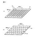
圖1係分解顯示表示本發明之一例的蒸鍍遮罩之金屬遮罩與樹脂遮罩之概略斜視圖,(a)係金屬遮罩之概略斜視圖,(b)係樹脂遮罩之概略斜視圖。Fig. 1 is an exploded view showing a schematic perspective view of a metal mask and a resin mask of a vapor deposition mask showing an example of the present invention, (a) is a schematic perspective view of the metal mask, and (b) is a schematic perspective view of the resin mask Figure.
圖2(a),(c),(d)係從顯示本發明之一例的蒸鍍遮罩之金屬遮罩側而視之正面圖,(b)係顯示表示本發明之一例的蒸鍍遮罩之概略剖面圖。Figure 2 (a), (c), (d) are front views from the metal mask side of the vapor deposition mask showing an example of the present invention, and (b) shows the vapor deposition mask showing an example of the present invention A schematic sectional view of the cover.
圖3係本發明之蒸鍍遮罩100之擴大剖面圖。FIG. 3 is an enlarged cross-sectional view of the
圖4(a)係樹脂遮罩之另外形態之斜視圖,(b)係其剖面圖。Fig. 4(a) is a perspective view of another form of the resin mask, and (b) is a cross-sectional view thereof.
圖5係顯示本發明之蒸鍍遮罩100之另外形態之正面圖。FIG. 5 is a front view showing another form of the
圖6係為了說明第1製造方法之工程圖。然而(a)~(f)係均為剖面圖。Fig. 6 is an engineering drawing for explaining the first manufacturing method. However, series (a) ~ (f) are all cross-sectional views.
圖7係為了說明第2製造方法之工程圖。然而(a)~(f)係均為剖面圖。Fig. 7 is an engineering drawing for explaining the second manufacturing method. However, series (a) ~ (f) are all cross-sectional views.
圖8係顯示陰影,和金屬遮罩之厚度的關係之概略剖面圖。Fig. 8 is a schematic cross-sectional view showing the relationship between the shadow and the thickness of the metal mask.
圖9係顯示金屬遮罩的縫隙,和樹脂遮罩之開口部的關係之部分概略剖面圖。9 is a partial schematic cross-sectional view showing the relationship between the gap of the metal mask and the opening of the resin mask.
圖10係顯示金屬遮罩的縫隙,和樹脂遮罩之開口部的關係之部分概略剖面圖。10 is a partial schematic cross-sectional view showing the relationship between the gap of the metal mask and the opening of the resin mask.
於以下,對於本發明之蒸鍍遮罩100,使用圖面具體地加以說明。Hereinafter, the
圖1(a)係構成顯示本發明之一例的蒸鍍遮罩之金屬遮罩之概略斜視圖,圖1(b)係構成顯示本發明之一例的蒸鍍遮罩之樹脂遮罩之概略斜視圖。圖2(a)係從顯示本發明之一例的蒸鍍遮罩之金屬遮罩側而視之正面圖,圖2(b)係顯示表示本發明之一例的蒸鍍遮罩之概略剖面圖。圖3係本發明之蒸鍍遮罩100之擴大剖面圖。然而,圖1~3同時為了強調金屬遮罩之所設置之縫隙及設置於蒸鍍遮罩之開口部,而擴大對於全體而言之比率而記載。Fig. 1(a) is a schematic perspective view of a metal mask constituting an evaporation mask showing an example of the present invention, and Fig. 1(b) is a schematic oblique view of a resin mask constituting an evaporation mask showing an example of the present invention Figure. Fig. 2(a) is a front view from the metal mask side of the vapor deposition mask showing an example of the present invention, and Fig. 2(b) is a schematic cross-sectional view showing the vapor deposition mask of an example of the present invention. Figure 3 is an enlargement of the
如圖1,2所示,本發明之蒸鍍遮罩100係採取層積設置有縫隙15之金屬遮罩10,和位置於金屬遮罩10的表面(對於圖2(b)所示之情況係金屬遮罩10之下面),將對應於蒸鍍製作之圖案之開口部25加以複數配列於縱橫之樹脂遮罩20的構成。As shown in Figures 1 and 2, the
在此,將本發明之蒸鍍遮罩100的質量,和僅由以往公知的金屬所構成之蒸鍍遮罩的質量,假定蒸鍍遮罩全體的厚度為相同而做比較時,僅以往公知的蒸鍍遮罩之金屬材料的一部分置換成樹脂材料的部分,本發明之蒸鍍遮罩100的質量變輕。另外,對於使用僅從金屬所構成之蒸鍍遮罩,為了謀求輕量化,係有必要薄化該蒸鍍遮罩之厚度等,但對於薄化蒸鍍遮罩之厚度情況係在將蒸鍍遮罩做為大型化時,引起有對於蒸鍍遮罩發生歪曲之情況,或耐久性下降之情況。另一方面,如根據本發明之蒸鍍遮罩,即使有做為大型化時之歪曲,或欲滿足耐久性而加厚蒸鍍遮罩全體之厚度的情況,經由樹脂遮罩20之存在,亦可較僅由金屬所形成之蒸鍍遮罩謀求輕量化者。以下,對於各自加以具體地說明。Here, when the quality of the
(樹脂遮罩)(Resin mask)
樹脂遮罩20係由樹脂加以構成,如圖1,2所示,將對應於蒸鍍製作於與縫隙15重疊之位置的圖案之開口部25,加以複數配列於縱橫。然而,在本申請說明書中進行蒸鍍製作之圖案係指作為呈使用該蒸鍍遮罩而製作之圖案,例如,對於將該蒸鍍遮罩使用於有機電激發光元件之有機層的形成情況,係為該有機層之形狀。另外,在本發明中,舉例說明將開口部複數配列於縱橫的例,開口部25係如設置於與縫隙重疊之位置即可,而縫隙15則對於僅配列1列於縱方向或橫方向之情況,係如設置開口部25於與該1列之縫隙15重疊之位置即可。The
樹脂遮罩20係可適宜選擇以往公知之樹脂材料而使用,對於此材料並無特別加以限定,但可經由雷射加工等而形成高精細之開口部25,使用在熱或經時之尺寸變化率或吸濕率小,輕量之材料為佳。作為如此之材料係可舉出聚醯亞胺樹脂,聚醯胺樹脂,聚醯胺醯亞胺樹脂,聚酯樹脂,聚乙烯樹脂,聚乙烯醇樹脂,聚丙烯樹脂,聚碳酸酯樹脂,聚苯乙烯樹脂,聚丙烯腈樹脂,乙烯乙酸乙烯共聚物樹脂,乙烯-乙烯醇共聚物樹脂,乙烯甲基丙烯酸共聚物樹脂,聚氯乙烯樹脂,聚偏二氯乙烯樹脂,玻璃紙,離子交聯聚合物樹脂等。在於上述例示的材料之中,其熱膨脹係數為16ppm/℃以下之樹脂材料為佳,吸濕率為1.0%以下之樹脂材料為佳,而具備此雙方條件之樹脂材料特別佳。在本發明中,樹脂遮罩20則如上述,與金屬材料做比較,由可形成高精細之開口部25之樹脂材料加以構成。隨之,可作為具有高精細之開口部25之蒸鍍遮罩100者。The
對於樹脂遮罩20之厚度亦無特別加以限定,但在使用本發明之蒸鍍遮罩100而進行蒸鍍時,對於為了防止對於蒸鍍作成之圖案產生有不充分之蒸鍍部分,也就是成為較作為目的之蒸鍍膜厚為薄膜厚之蒸鍍部分,所謂陰影之情況,樹脂遮罩20係僅可能為薄者為佳。但對於樹脂遮罩20之厚度不足3μm之情況,容易產生有針孔等之缺陷,另外變形等之風險變高。另一方面,當超過25μm時會產生陰影的發生。當考慮此點時,樹脂遮罩20之厚度係為3μm以上25μm以下者為佳。由將樹脂遮罩20之厚度作為此範圍內者,可降低針孔等缺陷或變形等之風險,且可有效果地防止陰影的發生者。特別是由將樹脂遮罩20之厚度作為3μm以上10μm以下,更理想為4μm以上8μm以下者,可更有效果地防止形成超過300ppi之高精細圖案時之陰影的影響者。然而,在本發明之蒸鍍遮罩100中,金屬遮罩10與樹脂遮罩20係亦可直接加以接合,而亦可藉由黏著劑層加以接合,但對於藉由黏著劑層而接合金屬遮罩10與樹脂遮罩20之情況,係考慮上述陰影的點,樹脂遮罩20與黏著劑層之合計厚度則呈成為3μm以上25μm以下,理想為3μm以上10μm,特別理想為4μm以上8μm以下之範圍內地設定者為佳。The thickness of the
對於開口部25的形狀,尺寸並無特別限定,如為對應於蒸鍍製作之圖案的形狀,尺寸即可。另外,如圖2(a)所示,對於鄰接之開口部25之橫方向的間距P1,或縱方向之間距P2亦可對應於蒸鍍製作之圖案而作適宜設定者。The shape of the
對於設置開口部25之位置,或開口部25的數量亦無特別地限定,於與縫隙15重疊之位置設置1個亦可,而亦可於縱方向或者橫方向設置複數個。例如,如圖2(c)所示,縫隙延伸於縱方向之情況,與該縫隙15重疊之開口部25則設置2個以上於橫方向亦可。The position where the
對於開口部25之剖面形狀亦無特別限定,形成開口部25之樹脂遮罩的對面之端面彼此則為略平行亦可,但如圖2(b)或圖3所示,開口部25係其剖面形狀為具有呈朝向蒸鍍源而擴散之形狀者為佳。換言之,具有朝向金屬遮罩10側而擴散之推拔面者為佳。經由將開口部25之剖面形狀作為該構成之時,使用本發明之蒸鍍遮罩而進行蒸鍍時,可防止對於蒸鍍作成之圖案產生有陰影情況。對於推拔角θ係可考慮樹脂遮罩20之厚度等而作適宜設定,但連結在樹脂遮罩之開口部的下底前端與同樣在樹脂遮罩之開口部的上底前端的角度(θ)則為25°~65°之範圍內為佳。特別是在此範圍內之中,亦較使用之蒸鍍機之蒸鍍角度為小之角度者為佳。更且,在圖2(b)或圖3中,形成開口部25之端面25a係呈現直線形狀,但並不限定於此,而於外面成為凸的彎曲形狀,也就是開口部25之全體形狀成為碗形狀亦可。具有如此剖面形狀之開口部25係例如在開口部25之形成時,由適宜調整雷射之照射位置,或雷射之照射能量,或者進行階段性地使照射位置之多階段的雷射照射者而可形成。The cross-sectional shape of the
樹脂遮罩20係從使用樹脂材料的情況,而未經由使用於以往之金屬加工的加工法,例如,蝕刻加工法或切削等之加工方法,可形成開口部25。也就是,對於開口部25之形成方法並無特別限定,而可使用各種加工方法,例如,可形成高精細之開口部25的雷射加工法,或精密沖壓加工,光微影加工等而形成開口部25者。對於經由雷射加工法等而形成開口部25的方法係後述之。The
作為蝕刻加工法,例如,可使用從噴射噴嘴,以特定噴霧壓力將蝕刻材噴霧之噴塗法,浸漬於充填有蝕刻材之蝕刻液中蝕刻法,滴下蝕刻材之旋轉蝕刻法等之濕蝕刻法,或利用氣體,電漿等之乾蝕刻法者。As the etching method, for example, a spraying method in which an etching material is sprayed from a spray nozzle at a specific spray pressure, an etching method in which an etching material is filled in an etching solution, and a spin etching method in which the etching material is dropped are used. , Or dry etching using gas, plasma, etc.
另外,在本發明中,從作為蒸鍍遮罩100之構成而使用樹脂遮罩20之情況,於使用此蒸鍍遮罩100而進行蒸鍍時,對於樹脂遮罩20之開口部25係加上非常高的熱,從形成樹脂遮罩20之開口部25之端面25a(參照圖3),產生有氣體,會產生有使蒸鍍裝置內之真空度降低等之虞。隨之,當考慮此點時,如圖3所示,對於形成樹脂遮罩20之開口部25之端面25a,係設置有阻障層26者為佳。由形成阻障層26者,可防止從形成樹脂遮罩20之開口部25之端面25a產生氣體者。In addition, in the present invention, from the case where the
阻障層26係可使用無機氧化物或無機氮化物,金屬之薄膜層或蒸鍍層。作為無機氧化物係可使用鋁或矽素,銦,錫,鎂之氧化物,作為金屬係可使用鋁等。阻障層26之厚度係為0.05μm~1μm程度為佳。The
更且,阻障層係被覆樹脂遮罩20之蒸鍍源側表面者為佳。經由以阻障層26被覆樹脂遮罩20之蒸鍍源側表面之時而阻障性更提升。阻障層係為無機氧化物,及無機氮化物之情況係經由各種PVD法,CVD法而形成者為佳。金屬之情況係經由真空蒸鍍法而形成為佳。然而,在此所稱之樹脂遮罩20之蒸鍍源側表面係指為樹脂遮罩20之蒸鍍源側之表面全體亦可,亦可為在樹脂遮罩20之蒸鍍源側之表面,僅從金屬遮罩露出之部分。Furthermore, it is preferable that the barrier layer coat the surface of the vapor deposition source side of the
圖4(a)係樹脂遮罩之另外形態之斜視圖,(b)係其剖面圖。Fig. 4(a) is a perspective view of another form of the resin mask, and (b) is a cross-sectional view thereof.
如圖4所示,對於樹脂遮罩20上,係形成有延伸於樹脂遮罩20之縱方向,或者橫方向(圖4之情況係縱方向)的溝28者為佳。在蒸鍍時加上熱的情況,樹脂遮罩20則產生熱膨脹,經由此而有對於開口部25之尺寸或位置產生變化的可能性,但由形成該溝28者而可吸收樹脂遮罩的膨脹,經由在樹脂遮罩之各處產生的熱膨脹產生累積而可防止樹脂遮罩20作為全體而膨脹於特定之方向,而開口部25之尺寸或位置產生變化者。As shown in FIG. 4, it is preferable that the
然而,在圖4中,於開口部25之間形成有延伸於縱方向的溝28,但並不限定於此,而亦可於開口部25之間形成有延伸於橫方向的溝。更且,並不限定於開口部25之間,而亦可形成溝於與開口部25重疊之位置。更且,亦可以組合此等之形態而構成溝者。However, in FIG. 4, the
對於溝28之深度或寬度並無特別限定,但對於溝28的深度過深之情況,或寬度過寬的情況,係從有樹脂遮罩20之剛性降低之傾向情況,必須考慮此點而設定。另外,對於溝的剖面形狀亦無特別加以限定,而U字形狀或V字形狀等,如考慮加工方法等而任意選擇即可。The depth or width of the
(金屬遮罩)(Metal mask)
金屬遮罩10係由金屬加以構成,從該金屬遮罩10的正面而視時,於與開口部25重疊的位置,換言之,可看到配置於樹脂遮罩20之所有的開口部25之位置,複數列配置有延伸於縱方向或橫方向之縫隙15。然而,在圖1,2中,延伸於金屬遮罩10之縱方向之縫隙15則連續配置於橫方向。另外,在本發明中,舉例說明縫隙15作為複數列配置有延伸於縱方向或橫方向之縫隙15的例,但縫隙15係僅配置1列於縱方向或橫方向亦可。The
對於縫隙15之寬度W並無特別限定,但至少呈較鄰接之開口部25間之間距為短地加以設計為佳。具體而言,如圖2(a)所示,對於縫隙15延伸於縱方向之情況,縫隙15之橫方向的寬度W係作為較鄰接於橫方向之開口部25之間距P1為短者為佳。同樣地,雖未圖示,但對於縫隙15延伸於橫方向之情況,縫隙15之縱方向的寬度係作為較鄰接於縱方向之開口部25之間距P2為短者為佳。另一方面,對於縫隙15延伸於縱方向情況之縱方向的長度L係無特別加以限定,如對應於金屬遮罩10之縱的長度及設置於樹脂遮罩20之開口部25之位置而作適宜設計即可。The width W of the
另外,連續延伸於縱方向或者橫方向之縫隙15則經由橋接器18而分割成複數亦可。然而,圖2(d)係從蒸鍍遮罩100之金屬遮罩10側而視之正面圖,顯示連續延伸於圖2(a)所示之縱方向的1個縫隙15則經由橋接器18而分割成複數(縫隙15a,15b)的例。對於橋接器18的寬度並無特別限定,但為5μm~20μm程度為佳。由將橋接器18的寬度作為此範圍者,可有效果地提高金屬遮罩10之剛性者。對於橋接器18之配置位置亦無特別限定,但分割後之縫隙則呈與2個以上的開口部25重疊地配置橋接器18者為佳。In addition, the
對於形成於金屬遮罩10之縫隙15之剖面形狀亦無特別加以限定,但與在上述樹脂遮罩20之開口部25同樣,如圖3所示,具有如朝向蒸鍍源擴散之形狀者為佳。The cross-sectional shape of the
對於金屬遮罩10之材料並無特別限定,可在蒸鍍遮罩之領域適宜選擇以往公知的構成而使用,例如,可舉出不鏽鋼,鐵鎳合金,鋁合金等之金屬材料者。其中,因鐵鎳合金之不變鋼材係經由熱的變形為少之故而可適合使用。The material of the
另外,在使用本發明之蒸鍍遮罩100而對於基板上進行蒸鍍時,對於配置磁鐵等於基板後方,經由磁力而吸引基板前方之蒸鍍遮罩100為必要之情況,係以磁性體形成金屬遮罩10者為佳。作為磁性體之金屬遮罩10係可舉出純鐵,碳素鋼,W鋼,Cr鋼、Co鋼、KS鋼、MK鋼、NKS鋼、Cunico鋼、Al-Fe合金等。另外,對於形成金屬遮罩10之材料本身並非磁性體之情況,係於該材料經由分散上述磁性體之粉末而賦予磁性於金屬遮罩10亦可。In addition, when vapor deposition is performed on a substrate using the
對於金屬遮罩10的厚度並無特別限定,但為5μm~100μm程度為佳。考慮在蒸鍍時之陰影的防止情況,金屬遮罩10之厚度係薄者為佳,但作為較5μm為薄之情況,破裂或變形的風險升高之同時,有著裝卸變為困難之可能性。但在本發明中,金屬遮罩10係從與樹脂遮罩20作為一體化之情況,即使金屬遮罩10之厚度為非常薄之5μm情況,亦可使破裂或變形的風險降低,如為5μm以上而可使用。然而,對於作為較100μm為厚之情況,係因會產生陰影的發生而並不理想。The thickness of the
以下,對於使用圖8(a)~圖8(c)而對於陰影之發生,和金屬遮罩10之厚度的關係具體地加以說明。如圖8(a)所示,對於金屬遮罩10之厚度為薄之情況,從蒸鍍源朝向蒸鍍對象物釋放之蒸鍍材係未衝突於金屬遮罩10之縫隙15之內壁面,或未設置有金屬遮罩10之樹脂遮罩20側的表面,而通過金屬遮罩10之縫隙15及樹脂遮罩20之開口部25而到達至蒸鍍對象物。經由此,成為可對於蒸鍍對象物上,以均一的膜厚形成蒸鍍圖案。也就是可防止陰影的發生者。另一方面,如圖8(b)所示,對於金屬遮罩10的厚度為厚之情況,例如,金屬遮罩10之厚度為超過100μm之厚度情況,從蒸鍍源所釋放之蒸鍍材的一部分係衝突於金屬遮罩10之縫隙15之內壁面,或未形成有金屬遮罩10之樹脂遮罩20側的表面,而無法到達至蒸鍍對象物。無法到達至蒸鍍對象物之蒸鍍材越多,產生有成為較對於蒸鍍對象物作為目的之蒸鍍膜厚為薄膜厚之未蒸鍍部分,而發生有陰影者。Hereinafter, the relationship between the occurrence of shadows and the thickness of the
對於充分防止陰影產生,係如圖8(c)所示,將縫隙15之剖面形狀,作為具有呈朝向蒸鍍源擴散之形狀者為佳。由作為如此之剖面形狀者,將會產生於蒸鍍遮罩100之歪曲防止,或者耐久性之提昇做為目的,即使為加厚蒸鍍遮罩全體厚度之情況,從蒸鍍源所釋放之蒸鍍材亦未衝突於縫隙15之該表面,或縫隙15之內壁面等,而可使蒸鍍材到達至蒸鍍對象物者。更具體而言,連結在金屬遮罩10之縫隙15的下底前端,和相同在金屬遮罩10之縫隙15的上底前端之直線與金屬遮罩10的底面之所成角度為在25°~65°之範圍內為佳。特別是在此範圍內之中,亦較使用之蒸鍍機之蒸鍍角度為小之角度者為佳。由作為如此之剖面形狀者,將會產生於蒸鍍遮罩100之歪曲防止,或者耐久性之提昇做為目的,即使將加厚金屬遮罩10作為比較厚之情況,從蒸鍍源所釋放之蒸鍍材亦未衝突於縫隙15之內壁面等,而可使蒸鍍材到達至蒸鍍對象物者。由此,可更有效果地防止陰影發生者。然而,圖8係為了說明陰影的發生,和金屬遮罩10之縫隙15的關係之部分概略剖面圖。然而,在圖8(c)中,金屬遮罩10之縫隙15則成為具有朝向於蒸鍍源側而擴散之剖面形狀,樹脂遮罩20之開口部25的對面之端面係成為略平行,但對於為了更有效果地防止陰影的發生,金屬遮罩10之縫隙,及樹脂遮罩20之開口部25係同時其剖面形狀則成為具有朝向於蒸鍍源側而擴散之形狀者為佳。To sufficiently prevent the generation of shadows, as shown in FIG. 8(c), the cross-sectional shape of the
圖5係顯示本發明之蒸鍍遮罩100之另外形態之正面圖。FIG. 5 is a front view showing another form of the
如圖5所示,在從蒸鍍遮罩100之金屬遮罩10側而視的正面圖中,將可從金屬遮罩之縫隙15而視之形成於樹脂遮罩20之開口部25,相互不同地配置於橫方向。也就是將鄰接於橫方向之開口部25偏移配置於縱方向亦可。經由如此地配置而即使有樹脂遮罩20產生熱膨脹之情況,可經由開口部25而吸收在各處產生之膨脹者,可防止膨脹累積而產生大的變形者。As shown in FIG. 5, in the front view from the side of the
另外,如圖5所示,形成於樹脂遮罩20之開口部25係無需使其對應於1畫素,而例如彙整2畫素~10畫素作為一個開口部25亦可。In addition, as shown in FIG. 5, the
圖9(a)~(d)係顯示金屬遮罩之縫隙,與樹脂遮罩之開口部的關係之部分概略剖面圖,在圖示之形態中,經由金屬遮罩之縫隙15與樹脂遮罩之開口部25所形成之開口全體的剖面形狀呈顯階梯狀。如圖9所示,由將開口全體之剖面形狀作為具有朝向於蒸鍍源側而擴散之階梯狀者而可有效果地防止陰影的發生者。金屬遮罩之縫隙15或樹脂遮罩20剖面形狀係如圖9(a)所示,對面之端面成為略平行亦可,但如圖9(b),(c)所示,僅金屬遮罩之縫隙15,樹脂遮罩之開口部之任一方則具有朝向於蒸鍍源側而擴散之剖面形狀構成亦可。然而如在上述所說明地,對於為了更有效果地防止陰影的發生,金屬遮罩之縫隙15及樹脂遮罩之開口部25係如圖3或圖9(d)所示,同時具有朝向於蒸鍍源側而擴散之剖面形狀者為佳。Figure 9 (a) ~ (d) are partial schematic cross-sectional views showing the relationship between the gap of the metal mask and the opening of the resin mask. In the illustrated form, the
對於在成為上述階梯狀之剖面的平坦部(在圖9之符號(×))之寬度並無特別限定,但對於平坦部(×)之寬度不足1μm之情況,係經由金屬遮罩的縫隙之干擾,而有陰影之發生防止效果下降之傾向。隨之,當考慮此點時,平坦部(×)之寬度係為1μm以上者為佳。對於理想之上限值係無特別限定,而可考慮樹脂遮罩之開口部尺寸,或鄰接之開口部的間隔等而作適宜設定,作為一例係為20μm程度。The width of the flat portion (the symbol (×) in FIG. 9) that becomes the stepped cross-section is not particularly limited. However, when the width of the flat portion (×) is less than 1 μm, the width is through the gap of the metal mask. Interference, and there is a tendency to prevent the occurrence of shadows from decreasing. Then, when considering this point, the width of the flat portion (×) is preferably 1 μm or more. The ideal upper limit is not particularly limited, and can be appropriately set in consideration of the size of the opening of the resin mask, the interval between adjacent openings, and the like, and is about 20 μm as an example.
然而,在上述圖9(a)~(d)中,顯示對於縫隙延伸於縱方向之情況,與該縫隙15重疊之開口部25則設置1個於橫方向的例,但如圖10所示,對於縫隙延伸於縱方向之情況,與該縫隙15重疊之開口部25則設置2個以上於橫方向亦可。圖10中,金屬遮罩之縫隙15及樹脂遮罩之開口部25係同時具有朝向於蒸鍍源側而擴散之剖面形狀,與該縫隙15重疊之開口部25則設置2個以上於橫方向。However, in the above figures 9(a) to (d), for the case where the slit extends in the vertical direction, the
(蒸鍍遮罩之製造方法)(Method of manufacturing vapor deposition mask)
接著,對於本發明之蒸鍍遮罩裝置之製造方法加以說明。Next, the manufacturing method of the vapor deposition mask device of the present invention will be described.
(第1製造方法)(First manufacturing method)
圖6係為了說明第1製造方法之工程圖。然而(a)~(f)係均為剖面圖。Fig. 6 is an engineering drawing for explaining the first manufacturing method. However, series (a) ~ (f) are all cross-sectional views.
第1製造方法係具備:貼合設置有縫隙之金屬遮罩與樹脂板的工程,和於含有金屬之框體上,固定貼合有前述樹脂板之金屬遮罩的工程,和從前述金屬遮罩側照射雷射,於前述樹脂板上於縱橫形成複數列之與需蒸鍍製作之圖案相對應之開口部之工程者。以下,對於各工程加以說明。The first manufacturing method includes: a process of bonding a metal mask provided with a gap and a resin plate, and a process of fixing the metal mask pasted with the resin plate to a frame containing metal, and a process of attaching the metal mask to the metal mask. The process of irradiating a laser on the side of the cover to form a plurality of rows of openings corresponding to the pattern to be made by vapor deposition on the aforementioned resin plate. Hereinafter, each process will be explained.
(貼合設置有縫隙之金屬遮罩與樹脂板的工程)(The process of bonding a metal mask with a gap and a resin board)
首先,準備設置有縫隙之金屬遮罩。在本方法中,對於所準備之金屬遮罩之製造方法係並無特別加以限定,而如適宜選擇可精確度佳地形成所期望之縫隙的方法即可。First, prepare a metal mask with gaps. In this method, the manufacturing method of the prepared metal mask is not particularly limited, and a method that can accurately form the desired gap can be selected as appropriate.
例如,如圖6(a)所示,準備金屬板61,於其兩面將光阻劑材62塗工。然而,作為所使用光阻劑材係使用處理性佳,有所期望之解像性之構成。之後,以形成有縫隙圖案的遮罩63遮蔽光阻劑材62,經由密著曝光而進行曝光,顯像。由此,如圖6(b)所示,於金屬板61之兩面形成光阻劑圖案64。接著,將此光阻劑圖案作為耐蝕刻遮罩而使用,經由2段蝕刻法而進行蝕刻加工。然而,2段蝕刻法係指於金屬板的兩面形成光阻劑圖案,進行來自單面側之蝕刻之後,於所形成之未貫通的凹部充填耐蝕刻性的樹脂,所謂充填材,之後由從另一面側進行蝕刻者而形成貫通孔之加工方法。在本方法中,並非由該2段蝕刻法,而採用從兩面同時進行蝕刻之方法亦可,但從加工精確度之觀點係使用2段蝕刻法者為佳。當蝕刻結束之後,洗淨除去光阻劑圖案。由此,如圖6(c)所示,於金屬板61形成所期望之縫隙65,得到金屬遮罩66。For example, as shown in FIG. 6(a), a
如圖6(d)所示,貼合金屬遮罩66與樹脂板67而獲得蒸鍍遮罩準備體。對於此方法亦無特別加以限定,例如亦可使用各種黏著劑,或使用具有本身黏著性之樹脂板。然而,金屬遮罩66與樹脂板67的尺寸係亦可為相同,但之後考慮對於以任意所進行之框體的固定,將樹脂板67之尺寸作為較金屬遮罩66為小,作為露出有金屬遮罩66之外周部分之狀態者為佳。As shown in FIG.6(d), the
(於含有金屬之框體固定貼合有前述樹脂板的金屬遮罩的工程)(The process of fixing the metal mask with the aforementioned resin plate to the frame containing metal)
接著,如圖6(e)所示,於含有金屬之框體68固定貼合有樹脂板67的金屬遮罩66。本方法係並無特別限定固定方法,例如,如採用點焊等以往公知的工程方法即可。Next, as shown in FIG. 6(e), the
(從金屬遮罩側照射雷射,於前述樹脂板上於縱橫形成複數列之與需蒸鍍製作之圖案相對應之開口部之工程)(The process of irradiating the laser from the side of the metal mask to form a plurality of rows of openings corresponding to the pattern to be made by vapor deposition on the aforementioned resin plate)
接著,從金屬遮罩66側通過縫隙65而照射雷射,將對應於蒸鍍製作於前述樹脂板67之圖案的開口部69,複數列形成於縱橫,作為樹脂遮罩70。對於在此所使用之雷射裝置係無特別加以限定,如使用以往公知之雷射裝置即可。由此,得到如圖6(f)所示之本發明之蒸鍍遮罩裝置80。Next, the laser is irradiated through the
(第2製造方法)(Second manufacturing method)
圖7係為了說明第2製造方法之工程圖。然而(a)~(f)係均為剖面圖。Fig. 7 is an engineering drawing for explaining the second manufacturing method. However, series (a) ~ (f) are all cross-sectional views.
第2製造方法,係具備:於含有金屬之框體上,固定設置有縫隙之金屬遮罩的工程,和貼合固定於前述框體之金屬遮罩,與樹脂板的工程,和從前述金屬遮罩側照射雷射,將對應於蒸鍍製作於前述樹脂板之圖案之開口部,複數列形成於縱橫之工程者。也就是,在上述說明之第1製造方法中,在貼合金屬遮罩66與樹脂板67之後,以框體68固定金屬遮罩66,但在第2製造方法中,首先將金屬遮罩66固定於框體68,之後貼合樹脂板67。The second manufacturing method includes: a process of fixing a metal mask provided with a gap on a frame containing metal, a process of attaching and fixing the metal mask to the frame, and a resin plate, and removing the metal The mask side is irradiated with a laser, and a plurality of rows of openings corresponding to the pattern made on the resin plate by vapor deposition are formed in the vertical and horizontal lines. That is, in the first manufacturing method described above, after bonding the
也就是,在第2製造方法中,如圖7(a)~(c)所示,對於製造金屬遮罩66之工程係與前述第1製造方法相同,如圖7(d)所示,將完成之金屬遮罩66固定於含有金屬之框體68之後,如圖7(e)所示,貼合金屬遮罩66與樹脂板67。之後,對於設置開口部65於樹脂板67而作為蒸鍍遮罩裝置80之工程,係如圖7(f)所示,與前述第1製造方法相同。That is, in the second manufacturing method, as shown in FIGS. 7(a) to (c), the process for manufacturing the
如此,如根據第1及第2製造方法,並非將均已完成之蒸鍍遮罩固定於框體,而對於固定於框體之狀態的樹脂板而言,因之後設置開口部之故,可特別使位置精確度提昇。然而,在以往公知的方法中,為了將決定開口之金屬遮罩對於框體而言拉伸的同時進行固定而開口位置座標精確度係降低。In this way, according to the first and second manufacturing methods, it is not necessary to fix both the vapor deposition masks to the frame body, but for the resin plate in the state fixed to the frame body, it is possible to provide openings afterwards. In particular, the position accuracy is improved. However, in the conventionally known method, in order to fix the metal mask that determines the opening to the frame while being stretched, the accuracy of the coordinates of the opening position is reduced.
另外,於固定於框體之狀態的樹脂板,設置開口部25時,準備預先設置有蒸鍍製作之圖案,即對應欲形成之開口部25之圖案的基準板,在將其基準板貼合於未設置有樹脂板之金屬遮罩66側的面之狀態,從金屬遮罩側,進行對應於基準板之圖案的雷射照射亦可。如根據此方法,可在注視貼合於樹脂板之基準板的圖案同時,進行雷射照射,所謂對面配合之狀態,形成開口部25,可形成開口之尺寸精確度極高之高精細的開口部25者。另外,此方法係從在固定於框體之狀態進行開口部25之形成情況,可做為不僅尺寸精確度,而對於位置精確度亦為優越之蒸鍍遮罩。In addition, when the
然而,對於使用上述方法之情況,係必須可從金屬遮罩66側,隔著樹脂板而由雷射照射裝置等辨識基準板之圖案者。作為樹脂板係對於具有某種程度厚度之情況係成為必須使用具有透明性之構成,但如在上述說明地,對於做為考慮陰影的影響為佳之厚度,例如3μm~25μm程度之厚度的情況,係即使加以著色的樹脂板,亦可辨識基準板之圖案者。However, in the case of using the above method, it is necessary to be able to recognize the pattern of the reference plate from the side of the
對於樹脂板與基準板的貼合方法亦無特別限定,例如,對於金屬遮罩66為磁性體之情況,係於基準板的後方配置磁鐵等,可由吸引樹脂板與基準板而加以貼合。除此之外,亦可使用靜電吸著法等而貼合者。作為基準板係可例如舉出具有特定之開口圖案之TFT基板,或光罩等者。The method of bonding the resin plate and the reference plate is not particularly limited. For example, when the
(輕薄工程)(Thin and light engineering)
另外,在本發明之製造方法中,於在上述說明之工程間,或者工程後,進行輕薄工程亦可。該工程係在本發明之製造方法之任意的工程,將金屬遮罩66之厚度,或樹脂遮罩70的厚度做為最佳化之工程。作為金屬遮罩66或樹脂遮罩70之理想的厚度係如適宜設定在上述說明之範圍內即可,在此之詳細的說明係省略之。In addition, in the manufacturing method of the present invention, a thin and light process may be performed between the processes described above or after the process. This process is an arbitrary process in the manufacturing method of the present invention, and the thickness of the
例如,對於作為成為樹脂遮罩70之樹脂板67或成為金屬遮罩66之金屬板61,使用較在上述說明之理想厚度為厚之構成的情況,在製造工程中,以單獨搬送金屬板61或樹脂板67時,可賦予對於搬送設置有樹脂板67於設置有凹部之金屬板61上之層積體時,或者在搬送在形成上述蒸鍍遮罩之工程所得到之蒸鍍遮罩100時優越之耐久性或搬送性者。另一方面,對於為了防止陰影的發生等,係在本發明之製造方法所得到之蒸鍍遮罩100的厚度係為最佳的厚度為佳。輕薄工程係在製造工程間,或者工程後中滿足耐久性或搬送性之同時,對於將蒸鍍遮罩100之厚度作為最佳化之情況而為有用之工程。For example, in the case where the
成為金屬遮罩66之金屬板61或金屬遮罩66之輕薄,即金屬遮罩之厚度的最佳化係可由於在上述所說明之工程間,或者工程後,可將未與金屬板61的樹脂板67接合側的面,或者未與金屬遮罩66之樹脂板67或樹脂遮罩20接合側的面,使用可蝕刻金屬板61或金屬遮罩66的蝕刻材而加以蝕刻者而實現。The lightness and thinness of the
對於成為樹脂遮罩70之樹脂板67或樹脂遮罩70之輕薄,即樹脂板67,樹脂遮罩70之厚度的最佳化亦為相同,可由於在上述所說明之任何工程間,或者工程後,可將未與樹脂板67的金屬板61或金屬遮罩66接合側的面,或者未與樹脂遮罩70之金屬遮罩66接合側的面,使用可蝕刻樹脂板67或樹脂遮罩70的材料之蝕刻材而加以蝕刻者而實現。另外,於形成蒸鍍遮罩100之後,由蝕刻加工金屬遮罩66,樹脂遮罩70雙方者,亦可將雙方的厚度作為最佳化者。For the lightness and thinness of the
(有機半導體元件之製造方法)(Method of manufacturing organic semiconductor device)
本發明之有機半導體元件之製造方法,係使用在上述說明之本發明之蒸鍍遮罩100而形成有機半導體元件者為特徵之構成。對於蒸鍍遮罩100係可直接使用在上述說明之本發明之蒸鍍遮罩100者,在此之詳細說明係省略之。如根據在上述所說明之本發明之蒸鍍遮罩,經由該蒸鍍遮罩100所具有之尺寸精確度高之開口部25,可形成具有高精細圖案之有機半導體元件者。作為以本發明之製造方法所製造之有機半導體元件,例如,可舉出有機電激發光元件之有機層,發光層,或陰極電極等。特別是本發明之有機半導體元件之製造方法係可最佳地使用於要求高精細圖案精確度之有機電激發光元件之R、G、B發光層之製造者。The method of manufacturing an organic semiconductor device of the present invention is formed by using the
61:金屬板61: metal plate
62:光阻劑材62: photoresist material
63:遮罩63: Mask
64:光阻劑圖案64: photoresist pattern
65:縫隙65: gap
66:金屬遮罩66: metal mask
67:樹脂板67: Resin board
68:框體68: Frame
69:開口部69: opening
70:樹脂遮罩70: Resin mask
80:蒸鍍遮罩裝置80: Evaporation mask device
Claims (14)
Translated fromChineseApplications Claiming Priority (2)
| Application Number | Priority Date | Filing Date | Title |
|---|---|---|---|
| JP2012004484 | 2012-01-12 | ||
| JP2012-004484 | 2012-01-12 |
Publications (2)
| Publication Number | Publication Date |
|---|---|
| TW202026139Atrue TW202026139A (en) | 2020-07-16 |
| TWI720818B TWI720818B (en) | 2021-03-01 |
Family
ID=48781584
Family Applications (7)
| Application Number | Title | Priority Date | Filing Date |
|---|---|---|---|
| TW105133715ATWI622662B (en) | 2012-01-12 | 2013-01-11 | Vapor deposition mask preparation |
| TW103117887ATWI498434B (en) | 2012-01-12 | 2013-01-11 | A method of manufacturing a vapor deposition mask, a method for producing a vapor deposition mask, and a method of manufacturing the organic semiconductor device |
| TW109105195ATWI720818B (en) | 2012-01-12 | 2013-01-11 | Evaporation mask, pattern manufacturing method, organic semiconductor device manufacturing method |
| TW107104773ATWI667138B (en) | 2012-01-12 | 2013-01-11 | Method for manufacturing vapor deposition mask, pattern, and method for manufacturing organic semiconductor element |
| TW104124249ATW201540855A (en) | 2012-01-12 | 2013-01-11 | Vapor deposition mask with metal plate |
| TW108121532ATWI687315B (en) | 2012-01-12 | 2013-01-11 | Vapor deposition mask, pattern manufacturing method, organic semiconductor element manufacturing method |
| TW102101284ATWI479041B (en) | 2012-01-12 | 2013-01-11 | A method of manufacturing a vapor deposition mask, a method for producing a vapor deposition mask, and a method of manufacturing the organic semiconductor device |
Family Applications Before (2)
| Application Number | Title | Priority Date | Filing Date |
|---|---|---|---|
| TW105133715ATWI622662B (en) | 2012-01-12 | 2013-01-11 | Vapor deposition mask preparation |
| TW103117887ATWI498434B (en) | 2012-01-12 | 2013-01-11 | A method of manufacturing a vapor deposition mask, a method for producing a vapor deposition mask, and a method of manufacturing the organic semiconductor device |
Family Applications After (4)
| Application Number | Title | Priority Date | Filing Date |
|---|---|---|---|
| TW107104773ATWI667138B (en) | 2012-01-12 | 2013-01-11 | Method for manufacturing vapor deposition mask, pattern, and method for manufacturing organic semiconductor element |
| TW104124249ATW201540855A (en) | 2012-01-12 | 2013-01-11 | Vapor deposition mask with metal plate |
| TW108121532ATWI687315B (en) | 2012-01-12 | 2013-01-11 | Vapor deposition mask, pattern manufacturing method, organic semiconductor element manufacturing method |
| TW102101284ATWI479041B (en) | 2012-01-12 | 2013-01-11 | A method of manufacturing a vapor deposition mask, a method for producing a vapor deposition mask, and a method of manufacturing the organic semiconductor device |
Country Status (6)
| Country | Link |
|---|---|
| US (7) | US9108216B2 (en) |
| JP (7) | JP5288072B2 (en) |
| KR (6) | KR102128735B1 (en) |
| CN (9) | CN105336855B (en) |
| TW (7) | TWI622662B (en) |
| WO (1) | WO2013105642A1 (en) |
Families Citing this family (106)
| Publication number | Priority date | Publication date | Assignee | Title |
|---|---|---|---|---|
| TWI461098B (en)* | 2012-01-12 | 2014-11-11 | Dainippon Printing Co Ltd | A method of manufacturing a vapor deposition mask, and a method of manufacturing an organic semiconductor device |
| CN105296920B (en) | 2012-01-12 | 2018-03-06 | 大日本印刷株式会社 | Layout deposition mask |
| CN105336855B (en)* | 2012-01-12 | 2020-08-04 | 大日本印刷株式会社 | Evaporation mask device preparation body |
| JP5895539B2 (en)* | 2012-01-12 | 2016-03-30 | 大日本印刷株式会社 | Evaporation mask |
| JP5895540B2 (en)* | 2012-01-12 | 2016-03-30 | 大日本印刷株式会社 | Evaporation mask |
| TWI671414B (en)* | 2013-03-26 | 2019-09-11 | 日商大日本印刷股份有限公司 | Vapor deposition mask, vapor deposition mask preparation body, method for producing vapor deposition mask, and method for producing organic semiconductor device |
| CN107855641A (en)* | 2013-04-12 | 2018-03-30 | 大日本印刷株式会社 | Deposition mask, deposition mask prepare body, the manufacture method of deposition mask and the manufacture method of organic semiconductor device |
| TWI624557B (en)* | 2013-04-12 | 2018-05-21 | 大日本印刷股份有限公司 | Vapor deposition mask, vapor deposition mask preparation body, method for manufacturing vapor deposition mask, and method for manufacturing organic semiconductor element |
| JP5455099B1 (en) | 2013-09-13 | 2014-03-26 | 大日本印刷株式会社 | Metal plate, metal plate manufacturing method, and mask manufacturing method using metal plate |
| JP6168944B2 (en)* | 2013-09-20 | 2017-07-26 | 株式会社ブイ・テクノロジー | Deposition mask |
| JP6331312B2 (en)* | 2013-09-30 | 2018-05-30 | 大日本印刷株式会社 | Vapor deposition mask manufacturing method and vapor deposition mask preparation |
| JP2015067892A (en)* | 2013-09-30 | 2015-04-13 | 大日本印刷株式会社 | Vapor deposition mask and organic semiconductor device manufacturing method |
| JP6394877B2 (en)* | 2013-09-30 | 2018-09-26 | 大日本印刷株式会社 | Vapor deposition mask, vapor deposition mask manufacturing method, vapor deposition mask preparation, framed vapor deposition mask, and organic semiconductor element manufacturing method |
| JP2015074826A (en)* | 2013-10-11 | 2015-04-20 | 株式会社ブイ・テクノロジー | Deposition mask, and manufacturing method thereof |
| JP5516816B1 (en) | 2013-10-15 | 2014-06-11 | 大日本印刷株式会社 | Metal plate, method for producing metal plate, and method for producing vapor deposition mask using metal plate |
| JP5780350B2 (en)* | 2013-11-14 | 2015-09-16 | 大日本印刷株式会社 | Vapor deposition mask, vapor deposition mask with frame, and method of manufacturing organic semiconductor element |
| JP6409701B2 (en)* | 2013-11-14 | 2018-10-24 | 大日本印刷株式会社 | Vapor deposition mask, vapor deposition mask with frame, and method of manufacturing organic semiconductor element |
| JP6288497B2 (en)* | 2013-12-13 | 2018-03-07 | 株式会社ブイ・テクノロジー | Mask and manufacturing method thereof |
| JP6357312B2 (en) | 2013-12-20 | 2018-07-11 | 株式会社ブイ・テクノロジー | Method for manufacturing film formation mask and film formation mask |
| KR102138625B1 (en)* | 2013-12-23 | 2020-07-29 | 엘지디스플레이 주식회사 | Thin film forming apparatus |
| JP5846287B1 (en)* | 2013-12-27 | 2016-01-20 | 大日本印刷株式会社 | Manufacturing method of vapor deposition mask with frame, tension device, manufacturing apparatus of organic semiconductor element, and manufacturing method of organic semiconductor element |
| JP6240960B2 (en)* | 2014-02-03 | 2017-12-06 | 株式会社ブイ・テクノロジー | Method for manufacturing film formation mask and film formation mask |
| JP6347112B2 (en)* | 2014-02-07 | 2018-06-27 | 大日本印刷株式会社 | Vapor deposition mask, vapor deposition mask preparation, vapor deposition mask manufacturing method, pattern manufacturing method, framed vapor deposition mask, and organic semiconductor element manufacturing method |
| JP2015148002A (en)* | 2014-02-07 | 2015-08-20 | 大日本印刷株式会社 | Vapor deposition mask, vapor deposition mask preparation, and method for manufacturing organic semiconductor element |
| CN103882375B (en)* | 2014-03-12 | 2016-03-09 | 京东方科技集团股份有限公司 | A kind of mask plate and preparation method thereof |
| JP6326885B2 (en)* | 2014-03-19 | 2018-05-23 | 大日本印刷株式会社 | Vapor deposition mask, vapor deposition mask preparation, and method for manufacturing organic semiconductor element |
| JP6511908B2 (en)* | 2014-03-31 | 2019-05-15 | 大日本印刷株式会社 | Tension method of deposition mask, method of manufacturing deposition mask with frame, method of manufacturing organic semiconductor device, and tension device |
| CN103952666B (en)* | 2014-04-22 | 2016-02-10 | 四川虹视显示技术有限公司 | evaporation mask plate tensioning method |
| CN103981485B (en)* | 2014-05-09 | 2016-07-06 | 合肥鑫晟光电科技有限公司 | Mask plate and manufacture method thereof |
| JP5641462B1 (en) | 2014-05-13 | 2014-12-17 | 大日本印刷株式会社 | Metal plate, metal plate manufacturing method, and mask manufacturing method using metal plate |
| CN110331365B (en)* | 2014-06-06 | 2021-10-01 | 大日本印刷株式会社 | Evaporation mask, precursor thereof, and method for producing organic semiconductor element |
| WO2015186632A1 (en)* | 2014-06-06 | 2015-12-10 | 大日本印刷株式会社 | Vapor deposition mask, vapor deposition mask with frame, vapor deposition mask precursor, and method for manufacturing organic semiconductor element |
| JP6323266B2 (en)* | 2014-09-03 | 2018-05-16 | 大日本印刷株式会社 | Deposition mask inspection method |
| US20170311411A1 (en)* | 2014-10-23 | 2017-10-26 | Sharp Kabushiki Kaisha | Deposition-mask manufacturing method, deposition mask, deposition device, and deposition method |
| DE102014116076A1 (en)* | 2014-11-04 | 2016-05-04 | Osram Opto Semiconductors Gmbh | Method for applying a material to a surface |
| JP6375906B2 (en)* | 2014-12-02 | 2018-08-22 | 大日本印刷株式会社 | Vapor deposition mask, vapor deposition mask preparation, framed vapor deposition mask, and organic semiconductor device manufacturing method |
| WO2016117535A1 (en)* | 2015-01-20 | 2016-07-28 | シャープ株式会社 | Deposition mask, manufacturing method |
| JP5994952B2 (en)* | 2015-02-03 | 2016-09-21 | 大日本印刷株式会社 | Vapor deposition mask manufacturing method, vapor deposition mask manufacturing apparatus, laser mask, and organic semiconductor element manufacturing method |
| EP3257964B1 (en)* | 2015-02-10 | 2019-11-13 | Dai Nippon Printing Co., Ltd. | Manufacturing method for deposition mask, metal sheet used for producing deposition mask, and manufacturing method for said metal sheet |
| JP6163586B2 (en) | 2015-04-17 | 2017-07-12 | 大日本印刷株式会社 | Deposition method of vapor deposition pattern, pressing member integrated with pressing plate, vapor deposition apparatus and organic semiconductor element manufacturing method |
| CH711107A1 (en)* | 2015-05-20 | 2016-11-30 | Glas Trösch Holding AG | Coupling device for thermogravimetric analysis. |
| JP2017008342A (en)* | 2015-06-17 | 2017-01-12 | 株式会社ブイ・テクノロジー | Film deposition mask and production method of film deposition mask |
| CN112267091B (en)* | 2015-07-03 | 2023-02-17 | 大日本印刷株式会社 | Method for manufacturing vapor deposition mask, method for manufacturing organic semiconductor element, method for manufacturing organic EL display, vapor deposition mask preparation body, and vapor deposition mask |
| JP6160747B2 (en)* | 2015-07-03 | 2017-07-12 | 大日本印刷株式会社 | Vapor deposition mask manufacturing method, vapor deposition mask preparation, organic semiconductor element manufacturing method, and vapor deposition mask |
| WO2017045122A1 (en)* | 2015-09-15 | 2017-03-23 | Applied Materials, Inc. | A shadow mask for organic light emitting diode manufacture |
| KR102430444B1 (en) | 2015-12-18 | 2022-08-09 | 삼성디스플레이 주식회사 | A mask assembly, apparatus and method for manufacturing a display apparatus using the same |
| CN112030102B (en)* | 2016-02-10 | 2022-12-06 | 鸿海精密工业股份有限公司 | Manufacturing method of evaporation mask |
| JP2017150017A (en) | 2016-02-23 | 2017-08-31 | 株式会社ジャパンディスプレイ | Method for manufacturing vapor deposition mask and method for manufacturing organic EL display |
| US20200299821A1 (en)* | 2016-03-18 | 2020-09-24 | Hon Hai Precision Industry Co., Ltd. | Vapor deposition mask, method for producing vapor deposition mask, and method for producing organic semiconductor element |
| WO2017168773A1 (en) | 2016-03-29 | 2017-10-05 | 鴻海精密工業股▲ふん▼有限公司 | Vapor deposition mask, method for manufacturing vapor deposition mask, vapor deposition method, and method for manufacturing organic el display device |
| JP6465075B2 (en) | 2016-05-26 | 2019-02-06 | 大日本印刷株式会社 | Vapor deposition mask, vapor deposition mask with frame, method for producing organic semiconductor element, and method for producing organic EL display |
| WO2018003766A1 (en) | 2016-06-28 | 2018-01-04 | 大日本印刷株式会社 | Vapor deposition mask, method for manufacturing organic semiconductor element, and method for manufacturing organic el display |
| JP7017032B2 (en) | 2016-06-28 | 2022-02-08 | 大日本印刷株式会社 | A vapor deposition mask, a method for manufacturing an organic semiconductor device, and a method for manufacturing an organic EL display. |
| KR102632617B1 (en)* | 2016-08-08 | 2024-02-02 | 삼성디스플레이 주식회사 | Mask assembly, apparatus and method for manufacturing a display apparatus using the same and display apparatus |
| KR102624714B1 (en) | 2016-09-12 | 2024-01-12 | 삼성디스플레이 주식회사 | Mask and method for preparing the mask assembly having the same |
| CN118159109A (en) | 2016-09-13 | 2024-06-07 | Lg伊诺特有限公司 | Metal plate for deposition mask, deposition mask and method for manufacturing the same |
| KR102455363B1 (en) | 2016-09-29 | 2022-10-18 | 다이니폰 인사츠 가부시키가이샤 | Vapor deposition mask package and vapor deposition mask packaging method |
| WO2018062300A1 (en)* | 2016-09-30 | 2018-04-05 | 大日本印刷株式会社 | Evaporation mask, evaporation mask provided with frame, evaporation mask prepared body, method for forming vapor deposition pattern, method for manufacturing organic semiconductor element, and method for manufacturing organic el display |
| WO2018058521A1 (en)* | 2016-09-30 | 2018-04-05 | 深圳市柔宇科技有限公司 | Metal mask for oled evaporation deposition and oled evaporation deposition method |
| JP6922179B2 (en)* | 2016-09-30 | 2021-08-18 | 大日本印刷株式会社 | A method for manufacturing a vapor deposition mask, an organic semiconductor element, and a method for manufacturing an organic EL display. |
| JP6926435B2 (en)* | 2016-10-03 | 2021-08-25 | 大日本印刷株式会社 | A method for manufacturing a vapor deposition mask, a method for manufacturing an organic semiconductor element, and a method for manufacturing an organic EL display. |
| CN109790615A (en) | 2016-10-06 | 2019-05-21 | 大日本印刷株式会社 | The manufacturing method of the manufacturing method of deposition mask, the manufacturing method of organic semiconductor device and organic el display |
| EP3524710B8 (en) | 2016-10-07 | 2024-01-24 | Dai Nippon Printing Co., Ltd. | Method of manufacturing deposition mask, intermediate product to which deposition mask is allocated, and deposition mask |
| US20180183014A1 (en)* | 2016-12-27 | 2018-06-28 | Int Tech Co., Ltd. | Light emitting device |
| JP6620899B2 (en)* | 2017-03-31 | 2019-12-18 | 大日本印刷株式会社 | Vapor deposition mask, vapor deposition mask with frame, vapor deposition mask preparation, vapor deposition pattern forming method, and organic semiconductor element manufacturing method |
| CN107058945B (en)* | 2017-04-20 | 2020-07-07 | 京东方科技集团股份有限公司 | Mask plate |
| CN206706184U (en)* | 2017-05-12 | 2017-12-05 | 京东方科技集团股份有限公司 | Mask plate and mask sheet |
| KR102300029B1 (en)* | 2017-07-27 | 2021-09-09 | 삼성디스플레이 주식회사 | Mask frame assembly, method for manufacturing the same and method for manufacturing a display apparatus using the same |
| US20190044068A1 (en)* | 2017-08-01 | 2019-02-07 | Wuhan China Star Optoelectronics Semiconductor Dis play Technology Co., Ltd. | Mask plate |
| US10510959B2 (en) | 2017-08-22 | 2019-12-17 | Wuhan China Star Optoelectronics Semiconductor Display Technology Co., Ltd. | Commissioning method and vapor deposition machine |
| CN107523787B (en)* | 2017-08-22 | 2019-08-02 | 武汉华星光电半导体显示技术有限公司 | A kind of adjustment method and evaporator |
| JP6300257B1 (en)* | 2017-08-31 | 2018-03-28 | 堺ディスプレイプロダクト株式会社 | Method for manufacturing film-forming mask |
| JP6497596B2 (en)* | 2017-09-14 | 2019-04-10 | 大日本印刷株式会社 | Intermediate of vapor deposition mask device |
| KR102411536B1 (en)* | 2017-10-11 | 2022-06-22 | 삼성디스플레이 주식회사 | Deposition mask manufacturing method and manufacturing apparatus thereof |
| US11121321B2 (en)* | 2017-11-01 | 2021-09-14 | Emagin Corporation | High resolution shadow mask with tapered pixel openings |
| KR102399595B1 (en)* | 2017-11-21 | 2022-05-19 | 엘지이노텍 주식회사 | Metal substrate and mask using the same |
| US10876199B2 (en)* | 2017-12-25 | 2020-12-29 | Sakai Display Products Corporation | Vapor deposition mask, vapor deposition method, and production method for organic EL display device |
| CN108227989B (en)* | 2018-01-02 | 2021-03-05 | 京东方科技集团股份有限公司 | Touch substrate and preparation method thereof, metal mask plate and display device |
| CN108281575B (en)* | 2018-01-26 | 2020-08-14 | 京东方科技集团股份有限公司 | Mask plate and manufacturing method thereof |
| JP6583446B2 (en)* | 2018-01-31 | 2019-10-02 | 大日本印刷株式会社 | Vapor deposition mask and organic semiconductor device manufacturing method |
| JP6996997B2 (en) | 2018-02-03 | 2022-01-17 | 日鉄ケミカル&マテリアル株式会社 | Metal-clad laminate and its manufacturing method |
| JP6658790B2 (en)* | 2018-04-19 | 2020-03-04 | 大日本印刷株式会社 | Evaporation mask, evaporation mask with frame, evaporation mask preparation, method of manufacturing evaporation mask, method of manufacturing organic semiconductor element, method of manufacturing organic EL display, and method of forming pattern |
| CN108914055B (en)* | 2018-07-05 | 2020-07-17 | 京东方科技集团股份有限公司 | A mask and evaporation equipment |
| JP7110776B2 (en)* | 2018-07-11 | 2022-08-02 | 大日本印刷株式会社 | Vapor deposition mask, method for manufacturing vapor deposition mask, and method for manufacturing organic EL display device |
| CN109166984A (en)* | 2018-09-12 | 2019-01-08 | 苏州蓝沛光电科技有限公司 | Mask and its manufacturing method for oled panel |
| CN109161853B (en)* | 2018-09-25 | 2020-12-18 | 合肥京东方光电科技有限公司 | Vapor deposition equipment and vapor deposition method |
| KR102137168B1 (en)* | 2018-10-15 | 2020-07-24 | 엘지전자 주식회사 | Processing method for fine metal mask and fine metal mask using the same |
| CN109208888A (en)* | 2018-10-22 | 2019-01-15 | 中国二冶集团有限公司 | The waste and old template reuse means of architectural engineering |
| US11773477B2 (en) | 2018-12-25 | 2023-10-03 | Dai Nippon Printing Co., Ltd. | Deposition mask |
| CN111378924A (en)* | 2018-12-25 | 2020-07-07 | 大日本印刷株式会社 | Vapor deposition mask |
| US11056277B2 (en) | 2018-12-28 | 2021-07-06 | Applied Materials, Inc. | Magnetized substrate carrier apparatus with shadow mask for deposition |
| CN109746141A (en)* | 2019-01-29 | 2019-05-14 | 杨鑫鹏 | A wood grain spraying board for furniture paint surface maintenance and spraying method and manufacturing process thereof |
| CN109881147A (en)* | 2019-02-01 | 2019-06-14 | 云谷(固安)科技有限公司 | Vapor deposition mask plate, preparation method, oled display substrate and display device |
| US10957512B1 (en)* | 2019-09-25 | 2021-03-23 | Applied Materials, Inc. | Method and device for a carrier proximity mask |
| CN210916231U (en)* | 2019-10-18 | 2020-07-03 | 昆山国显光电有限公司 | Mask plate |
| US11805678B2 (en) | 2019-11-21 | 2023-10-31 | Samsung Display Co., Ltd. | Display device, mask assembly, method of manufacturing the mask assembly, apparatus for manufacturing the display device, and method of manufacturing the display device |
| US20230043183A1 (en)* | 2020-01-03 | 2023-02-09 | Hunetplus Co., Ltd. | Flexible photo-patterned mask for organic light emitting display with high resolution and method for manufacturing the same |
| KR20210091382A (en) | 2020-01-13 | 2021-07-22 | 삼성디스플레이 주식회사 | Mask, method of manufacturing the same, and method of manufacturing display panel |
| KR20210113526A (en)* | 2020-03-06 | 2021-09-16 | 삼성디스플레이 주식회사 | Method of manufacturing mask, mask manufacture by the same, and method of manufacturing display apparatus |
| JP7749925B2 (en)* | 2020-03-13 | 2025-10-07 | 大日本印刷株式会社 | Evaluation method for deposition chamber of organic device manufacturing equipment |
| CN113817981B (en)* | 2020-06-18 | 2022-09-30 | 中国科学技术大学 | Mask and method of making the same |
| KR20220016383A (en)* | 2020-07-31 | 2022-02-09 | 삼성디스플레이 주식회사 | Mask and manufacturing method of mask |
| CN113224105B (en)* | 2021-07-08 | 2021-09-28 | 苏州芯聚半导体有限公司 | Colorization manufacturing method, color substrate and display device |
| KR20230020035A (en)* | 2021-08-02 | 2023-02-10 | 삼성디스플레이 주식회사 | Mask for Deposition |
| US20250146121A1 (en) | 2022-01-31 | 2025-05-08 | Dai Nippon Printing Co., Ltd. | Mask and method of manufacturing mask |
| JPWO2024128182A1 (en) | 2022-12-13 | 2024-06-20 |
Family Cites Families (79)
| Publication number | Priority date | Publication date | Assignee | Title |
|---|---|---|---|---|
| JPS5948059A (en) | 1982-09-13 | 1984-03-19 | Dainippon Ink & Chem Inc | Modified stevioside |
| JPS6376859A (en)* | 1986-09-19 | 1988-04-07 | Matsushita Electric Ind Co Ltd | Vapor deposition mask and its manufacturing method |
| JP3017752B2 (en) | 1989-07-26 | 2000-03-13 | 村上スクリーン株式会社 | Printing metal mask and manufacturing method thereof |
| JPH07300664A (en)* | 1994-04-28 | 1995-11-14 | Fujitsu Ltd | Metal mask manufacturing method and its reclaiming method |
| US6045671A (en)* | 1994-10-18 | 2000-04-04 | Symyx Technologies, Inc. | Systems and methods for the combinatorial synthesis of novel materials |
| DE69618162T2 (en) | 1995-08-24 | 2002-08-14 | Kabushiki Kaisha Toshiba, Kawasaki | Manufacturing process of a reflector |
| JPH09143758A (en) | 1995-11-22 | 1997-06-03 | Nippon Steel Corp | Resin-coated metal plate for container and can body having the resin-coated metal plate |
| JP2000173769A (en) | 1998-12-03 | 2000-06-23 | Toray Ind Inc | Manufacture of organic electric field light-emitting element |
| US6469439B2 (en) | 1999-06-15 | 2002-10-22 | Toray Industries, Inc. | Process for producing an organic electroluminescent device |
| US20100261159A1 (en)* | 2000-10-10 | 2010-10-14 | Robert Hess | Apparatus for assay, synthesis and storage, and methods of manufacture, use, and manipulation thereof |
| JP2002220656A (en) | 2000-11-22 | 2002-08-09 | Sanyo Electric Co Ltd | Mask for vapor deposition and manufacturing method therefor |
| JP4092914B2 (en) | 2001-01-26 | 2008-05-28 | セイコーエプソン株式会社 | MASK MANUFACTURING METHOD, ORGANIC ELECTROLUMINESCENT DEVICE MANUFACTURING METHOD |
| US7396558B2 (en) | 2001-01-31 | 2008-07-08 | Toray Industries, Inc. | Integrated mask and method and apparatus for manufacturing organic EL device using the same |
| JP4096567B2 (en) | 2001-01-31 | 2008-06-04 | 東レ株式会社 | Integrated mask, method for manufacturing organic EL element using integrated mask, and manufacturing apparatus therefor |
| JP4635348B2 (en)* | 2001-02-08 | 2011-02-23 | 凸版印刷株式会社 | Pattern forming mask and pattern forming apparatus using the same |
| JP2003332057A (en) | 2002-05-16 | 2003-11-21 | Dainippon Printing Co Ltd | Multi-face mask device for vacuum deposition used for manufacturing organic EL devices |
| CN100355104C (en)* | 2001-08-24 | 2007-12-12 | 大日本印刷株式会社 | Multi-face forming mask device for vacuum deposition |
| JP2003231964A (en) | 2001-12-05 | 2003-08-19 | Toray Ind Inc | Evaporation mask, its manufacturing process, organic electroluminescent device and its manufacturing process |
| KR100490534B1 (en) | 2001-12-05 | 2005-05-17 | 삼성에스디아이 주식회사 | Mask frame assembly for thin layer vacuum evaporation of Organic electro luminescence device |
| US6897164B2 (en) | 2002-02-14 | 2005-05-24 | 3M Innovative Properties Company | Aperture masks for circuit fabrication |
| JP2003272838A (en)* | 2002-03-14 | 2003-09-26 | Dainippon Printing Co Ltd | Masking material |
| JP2004043898A (en) | 2002-07-12 | 2004-02-12 | Canon Electronics Inc | Vapor deposition mask, and organic electroluminescence display device |
| JP2004055231A (en)* | 2002-07-17 | 2004-02-19 | Dainippon Printing Co Ltd | Multi-faced metal mask for vacuum deposition used for manufacturing organic EL devices |
| JP4104964B2 (en)* | 2002-12-09 | 2008-06-18 | 日本フイルコン株式会社 | MASK FOR FORMING THIN FILM PATTERN OF LAMINATED STRUCTURE COMPRISING PATTERNED MASK COATING AND SUPPORT AND METHOD FOR PRODUCING THE SAME |
| JP3990307B2 (en)* | 2003-03-24 | 2007-10-10 | 株式会社クラレ | Manufacturing method of resin molded product, manufacturing method of metal structure, chip |
| KR100534580B1 (en) | 2003-03-27 | 2005-12-07 | 삼성에스디아이 주식회사 | Deposition mask for display device and Method for fabricating the same |
| JPWO2004114021A1 (en)* | 2003-06-23 | 2006-08-03 | 三井化学株式会社 | Photosensitive composition and method for producing printed wiring board using the same |
| US9236279B2 (en) | 2003-06-27 | 2016-01-12 | Lam Research Corporation | Method of dielectric film treatment |
| JP2005042147A (en)* | 2003-07-25 | 2005-02-17 | Dainippon Screen Mfg Co Ltd | Method of producing mask for vapor deposition, and mask for vapor deposition |
| JP2005146338A (en)* | 2003-11-14 | 2005-06-09 | Sony Corp | Vapor deposition mask |
| JP2005154879A (en)* | 2003-11-28 | 2005-06-16 | Canon Components Inc | Metal mask for vapor deposition, and method of producing vapor deposition pattern using the same |
| JP2005174843A (en) | 2003-12-15 | 2005-06-30 | Sony Corp | Deposition mask and its manufacturing method |
| JP4434809B2 (en)* | 2004-03-29 | 2010-03-17 | 三洋電機株式会社 | Manufacturing method of semiconductor device |
| JP2008226859A (en)* | 2004-10-22 | 2008-09-25 | Seiko Epson Corp | Method for manufacturing organic electroluminescence device and organic electroluminescence device |
| JP4329740B2 (en) | 2004-10-22 | 2009-09-09 | セイコーエプソン株式会社 | Method for manufacturing organic electroluminescent device and organic electroluminescent device |
| JP4761569B2 (en) | 2004-12-21 | 2011-08-31 | アルバック シンガポール プライベート リミテッド | Deposition mask and mask assembly jig |
| JP4438710B2 (en) | 2005-07-20 | 2010-03-24 | セイコーエプソン株式会社 | Mask, mask chip, mask manufacturing method, and mask chip manufacturing method |
| JP5008849B2 (en) | 2005-09-08 | 2012-08-22 | ソニーモバイルディスプレイ株式会社 | Laser processing method and manufacturing method of display device having transparent resin layer |
| US20070148337A1 (en) | 2005-12-22 | 2007-06-28 | Nichols Jonathan A | Flame-perforated aperture masks |
| CN100482848C (en)* | 2006-06-12 | 2009-04-29 | 友达光电股份有限公司 | Shielding, evaporation device using same and manufacturing method of display panel |
| JP2008121060A (en)* | 2006-11-10 | 2008-05-29 | Mitsubishi Paper Mills Ltd | Method of manufacturing vacuum film-forming mask with resin and vacuum film-forming mask with resin |
| KR20080045886A (en)* | 2006-11-21 | 2008-05-26 | 삼성전자주식회사 | Mask for organic film deposition and manufacturing method thereof, and manufacturing method of organic light emitting display device comprising same |
| JP5255224B2 (en) | 2007-03-29 | 2013-08-07 | 三菱製紙株式会社 | Screen printing mask and method for producing screen printing mask |
| JP2008255449A (en)* | 2007-04-09 | 2008-10-23 | Kyushu Hitachi Maxell Ltd | Vapor deposition mask and manufacturing method thereof |
| CN100580905C (en) | 2007-04-20 | 2010-01-13 | 晶能光电(江西)有限公司 | Method for obtaining high quality margins of semiconductor devices fabricated on segmented substrates |
| JP2008274373A (en)* | 2007-05-02 | 2008-11-13 | Optnics Precision Co Ltd | Mask for vapor deposition |
| KR20080111967A (en) | 2007-06-20 | 2008-12-24 | 삼성전기주식회사 | Shadow mask |
| JP2009041054A (en) | 2007-08-07 | 2009-02-26 | Sony Corp | Mask for vapor deposition, its manufacturing method, and manufacturing method of display device |
| JP4985227B2 (en)* | 2007-08-24 | 2012-07-25 | 大日本印刷株式会社 | Vapor deposition mask, vapor deposition mask device, vapor deposition mask manufacturing method, vapor deposition mask device production method, and vapor deposition mask sheet-like member production method |
| JP2009052073A (en)* | 2007-08-24 | 2009-03-12 | Dainippon Printing Co Ltd | Sheet with vapor deposition mask, method for producing vapor deposition mask device, and method for producing sheet with vapor deposition mask |
| JP2009107208A (en)* | 2007-10-30 | 2009-05-21 | Mitsubishi Paper Mills Ltd | Screen printing mask and method for producing screen printing mask |
| KR101450728B1 (en) | 2008-05-28 | 2014-10-14 | 삼성디스플레이 주식회사 | Mask assembly and method of making same |
| JP5239800B2 (en) | 2008-07-24 | 2013-07-17 | 富士ゼロックス株式会社 | Optical waveguide film, method for manufacturing the same, and optical transceiver module |
| KR20100026655A (en) | 2008-09-01 | 2010-03-10 | 삼성모바일디스플레이주식회사 | Mask for thin film deposition and manufacturing method of oled using the same |
| KR101117645B1 (en) | 2009-02-05 | 2012-03-05 | 삼성모바일디스플레이주식회사 | Mask Assembly and Deposition Apparatus using the same for Flat Panel Display |
| JP5323581B2 (en) | 2009-05-08 | 2013-10-23 | 三星ディスプレイ株式會社 | Vapor deposition method and vapor deposition apparatus |
| KR101135544B1 (en)* | 2009-09-22 | 2012-04-17 | 삼성모바일디스플레이주식회사 | Mask Assembly, Fabrication method of the same and Deposition Apparatus using the same for Flat Panel Display device |
| CN104157694A (en) | 2009-09-30 | 2014-11-19 | 大日本印刷株式会社 | Substrate for flexible device, flexible device, thin film transistor and method for manufacturing same |
| JP5585813B2 (en) | 2010-02-05 | 2014-09-10 | 株式会社ブイ・テクノロジー | Laser processing equipment |
| JP5379717B2 (en) | 2010-02-24 | 2013-12-25 | 株式会社アルバック | Evaporation mask |
| KR101442941B1 (en)* | 2010-03-09 | 2014-09-22 | 샤프 가부시키가이샤 | Vapor deposition mask, vapor deposition apparatus and vapor deposition method |
| KR101434084B1 (en)* | 2010-05-28 | 2014-09-22 | 샤프 가부시키가이샤 | Evaporation mask, and production method and production apparatus for organic el element using evaporation mask |
| JP2012015463A (en) | 2010-07-05 | 2012-01-19 | V Technology Co Ltd | Yag laser annealing device and annealing method by yag laser light |
| JP2013021165A (en) | 2011-07-12 | 2013-01-31 | Sony Corp | Mask for vapor deposition, manufacturing method of mask for vapor deposition, electronic element, and manufacturing method of electronic element |
| JP5517308B2 (en) | 2011-11-22 | 2014-06-11 | 株式会社ブイ・テクノロジー | Mask manufacturing method, mask and mask manufacturing apparatus |
| JP5899585B2 (en)* | 2011-11-04 | 2016-04-06 | 株式会社ブイ・テクノロジー | Mask manufacturing method |
| JP5884543B2 (en)* | 2011-09-16 | 2016-03-15 | 株式会社ブイ・テクノロジー | Thin film pattern forming method, mask manufacturing method, and organic EL display device manufacturing method |
| TWI555862B (en) | 2011-09-16 | 2016-11-01 | V科技股份有限公司 | Evaporation mask, method for manufacturing the same and thinfilm pattern forming method |
| JP5804457B2 (en)* | 2011-10-06 | 2015-11-04 | 株式会社ブイ・テクノロジー | mask |
| JP5515025B2 (en)* | 2011-10-06 | 2014-06-11 | 株式会社ブイ・テクノロジー | Mask, mask member used therein, mask manufacturing method, and organic EL display substrate manufacturing method |
| JP5935179B2 (en)* | 2011-12-13 | 2016-06-15 | 株式会社ブイ・テクノロジー | Vapor deposition mask and vapor deposition mask manufacturing method |
| TWI461098B (en)* | 2012-01-12 | 2014-11-11 | Dainippon Printing Co Ltd | A method of manufacturing a vapor deposition mask, and a method of manufacturing an organic semiconductor device |
| CN105336855B (en)* | 2012-01-12 | 2020-08-04 | 大日本印刷株式会社 | Evaporation mask device preparation body |
| CN105296920B (en)* | 2012-01-12 | 2018-03-06 | 大日本印刷株式会社 | Layout deposition mask |
| CN103205704A (en)* | 2012-01-16 | 2013-07-17 | 昆山允升吉光电科技有限公司 | Vapor deposition mask |
| KR101978190B1 (en) | 2012-11-29 | 2019-05-15 | 삼성디스플레이 주식회사 | Polarizer and method of manufacturing the same |
| CN103045996A (en)* | 2012-12-10 | 2013-04-17 | 陕西科技大学 | Mask plate regulating device for evaporating organic electroluminescence device |
| JP6357312B2 (en)* | 2013-12-20 | 2018-07-11 | 株式会社ブイ・テクノロジー | Method for manufacturing film formation mask and film formation mask |
| JP6596106B2 (en)* | 2016-01-26 | 2019-10-23 | 鴻海精密工業股▲ふん▼有限公司 | Method of manufacturing vapor deposition mask and method of manufacturing organic light emitting diode using the vapor deposition mask |
- 2013
- 2013-01-11CNCN201510639737.2Apatent/CN105336855B/enactiveActive
- 2013-01-11TWTW105133715Apatent/TWI622662B/enactive
- 2013-01-11TWTW103117887Apatent/TWI498434B/enactive
- 2013-01-11TWTW109105195Apatent/TWI720818B/enactive
- 2013-01-11JPJP2013003070Apatent/JP5288072B2/enactiveActive
- 2013-01-11KRKR1020207006105Apatent/KR102128735B1/enactiveActive
- 2013-01-11CNCN201510639770.5Apatent/CN105331934A/enactivePending
- 2013-01-11WOPCT/JP2013/050422patent/WO2013105642A1/enactiveApplication Filing
- 2013-01-11USUS14/371,670patent/US9108216B2/enactiveActive
- 2013-01-11KRKR1020217011669Apatent/KR20210046847A/ennot_activeCeased
- 2013-01-11CNCN201510639577.1Apatent/CN105322102B/enactiveActive
- 2013-01-11CNCN201510639578.6Apatent/CN105322103B/enactiveActive
- 2013-01-11KRKR1020207018307Apatent/KR20200077625A/ennot_activeCeased
- 2013-01-11KRKR1020147016827Apatent/KR101972920B1/enactiveActive
- 2013-01-11CNCN201510639565.9Apatent/CN105349946A/enactivePending
- 2013-01-11CNCN201510639576.7Apatent/CN105322101B/enactiveActive
- 2013-01-11CNCN201380005292.1Apatent/CN104053813B/enactiveActive
- 2013-01-11TWTW107104773Apatent/TWI667138B/enactive
- 2013-01-11CNCN201510639596.4Apatent/CN105331927B/enactiveActive
- 2013-01-11KRKR1020197011496Apatent/KR102085707B1/enactiveActive
- 2013-01-11CNCN201510639768.8Apatent/CN105331928B/enactiveActive
- 2013-01-11TWTW104124249Apatent/TW201540855A/enunknown
- 2013-01-11TWTW108121532Apatent/TWI687315B/enactive
- 2013-01-11TWTW102101284Apatent/TWI479041B/enactive
- 2013-01-11KRKR1020147016626Apatent/KR101439218B1/enactiveActive
- 2013-06-03JPJP2013117238Apatent/JP6209867B2/enactiveActive
- 2015
- 2015-05-22USUS14/719,355patent/US9527098B2/enactiveActive
- 2016
- 2016-07-20USUS15/214,808patent/US10160000B2/enactiveActive
- 2017
- 2017-06-19JPJP2017119535Apatent/JP2017166074A/enactivePending
- 2018
- 2018-06-22USUS16/015,430patent/US10189042B2/enactiveActive
- 2018-11-08USUS16/184,288patent/US10391511B2/enactiveActive
- 2018-12-25JPJP2018241275Apatent/JP2019052378A/enactivePending
- 2019
- 2019-07-09USUS16/506,107patent/US10894267B2/enactiveActive
- 2020
- 2020-07-02JPJP2020114766Apatent/JP6835283B2/enactiveActive
- 2020-11-18USUS16/951,223patent/US11511301B2/enactiveActive
- 2021
- 2021-02-04JPJP2021016533Apatent/JP2021073382A/enactivePending
- 2022
- 2022-10-13JPJP2022164764Apatent/JP2022179744A/enactivePending
Also Published As
Similar Documents
| Publication | Publication Date | Title |
|---|---|---|
| TWI720818B (en) | Evaporation mask, pattern manufacturing method, organic semiconductor device manufacturing method | |
| TWI705150B (en) | Manufacturing method of vapor deposition mask, laminate, pattern manufacturing method, and organic semiconductor element manufacturing method | |
| TWI725466B (en) | Vapor deposition mask, vapor deposition mask with frame, vapor deposition mask manufacturing method, vapor deposition mask preparation body, pattern formation method, and organic semiconductor device manufacturing method |