TW202017193A - High density MIM capacitor structure - Google Patents
High density MIM capacitor structureDownload PDFInfo
- Publication number
- TW202017193A TW202017193ATW108116938ATW108116938ATW202017193ATW 202017193 ATW202017193 ATW 202017193ATW 108116938 ATW108116938 ATW 108116938ATW 108116938 ATW108116938 ATW 108116938ATW 202017193 ATW202017193 ATW 202017193A
- Authority
- TW
- Taiwan
- Prior art keywords
- conductive electrode
- layer
- dielectric
- layers
- dielectric structure
- Prior art date
Links
- 239000003990capacitorSubstances0.000titleclaimsabstractdescription201
- 239000000758substrateSubstances0.000claimsabstractdescription67
- 229910052751metalInorganic materials0.000claimsabstractdescription32
- 239000002184metalSubstances0.000claimsabstractdescription32
- 239000010410layerSubstances0.000claimsdescription391
- 239000011229interlayerSubstances0.000claimsdescription69
- 238000000034methodMethods0.000claimsdescription59
- 230000008569processEffects0.000claimsdescription42
- 238000005530etchingMethods0.000claimsdescription27
- 239000004020conductorSubstances0.000claimsdescription10
- 238000000151depositionMethods0.000claimsdescription6
- 235000012431wafersNutrition0.000description53
- 239000003989dielectric materialSubstances0.000description47
- -1Tungsten nitrideChemical class0.000description17
- VYPSYNLAJGMNEJ-UHFFFAOYSA-NSilicium dioxideChemical compoundO=[Si]=OVYPSYNLAJGMNEJ-UHFFFAOYSA-N0.000description16
- 230000009471actionEffects0.000description16
- 229910052581Si3N4Inorganic materials0.000description13
- 238000002161passivationMethods0.000description12
- 229910052721tungstenInorganic materials0.000description10
- 239000010937tungstenSubstances0.000description10
- RYGMFSIKBFXOCR-UHFFFAOYSA-NCopperChemical compound[Cu]RYGMFSIKBFXOCR-UHFFFAOYSA-N0.000description8
- 229910052782aluminiumInorganic materials0.000description8
- XAGFODPZIPBFFR-UHFFFAOYSA-NaluminiumChemical compound[Al]XAGFODPZIPBFFR-UHFFFAOYSA-N0.000description8
- 229910052802copperInorganic materials0.000description8
- 239000010949copperSubstances0.000description8
- 235000012239silicon dioxideNutrition0.000description8
- 239000000377silicon dioxideSubstances0.000description8
- 238000005229chemical vapour depositionMethods0.000description7
- WFKWXMTUELFFGS-UHFFFAOYSA-NtungstenChemical compound[W]WFKWXMTUELFFGS-UHFFFAOYSA-N0.000description7
- NRTOMJZYCJJWKI-UHFFFAOYSA-NTitanium nitrideChemical compound[Ti]#NNRTOMJZYCJJWKI-UHFFFAOYSA-N0.000description6
- 238000000231atomic layer depositionMethods0.000description6
- 230000004888barrier functionEffects0.000description6
- 238000005137deposition processMethods0.000description6
- 238000005240physical vapour depositionMethods0.000description6
- BASFCYQUMIYNBI-UHFFFAOYSA-NplatinumChemical compound[Pt]BASFCYQUMIYNBI-UHFFFAOYSA-N0.000description6
- RTAQQCXQSZGOHL-UHFFFAOYSA-NTitaniumChemical compound[Ti]RTAQQCXQSZGOHL-UHFFFAOYSA-N0.000description5
- 229910052715tantalumInorganic materials0.000description5
- GUVRBAGPIYLISA-UHFFFAOYSA-Ntantalum atomChemical compound[Ta]GUVRBAGPIYLISA-UHFFFAOYSA-N0.000description5
- MZLGASXMSKOWSE-UHFFFAOYSA-Ntantalum nitrideChemical compound[Ta]#NMZLGASXMSKOWSE-UHFFFAOYSA-N0.000description5
- 239000010936titaniumSubstances0.000description5
- 229910052719titaniumInorganic materials0.000description5
- 229910002367SrTiOInorganic materials0.000description4
- 230000001154acute effectEffects0.000description4
- MRELNEQAGSRDBK-UHFFFAOYSA-Nlanthanum(3+);oxygen(2-)Chemical compound[O-2].[O-2].[O-2].[La+3].[La+3]MRELNEQAGSRDBK-UHFFFAOYSA-N0.000description4
- 239000000463materialSubstances0.000description4
- 230000002093peripheral effectEffects0.000description4
- 229920002120photoresistant polymerPolymers0.000description4
- WNUPENMBHHEARK-UHFFFAOYSA-Nsilicon tungstenChemical compound[Si].[W]WNUPENMBHHEARK-UHFFFAOYSA-N0.000description4
- KJTLSVCANCCWHF-UHFFFAOYSA-NRutheniumChemical compound[Ru]KJTLSVCANCCWHF-UHFFFAOYSA-N0.000description3
- XUIMIQQOPSSXEZ-UHFFFAOYSA-NSiliconChemical compound[Si]XUIMIQQOPSSXEZ-UHFFFAOYSA-N0.000description3
- UGACIEPFGXRWCH-UHFFFAOYSA-N[Si].[Ti]Chemical compound[Si].[Ti]UGACIEPFGXRWCH-UHFFFAOYSA-N0.000description3
- UQZIWOQVLUASCR-UHFFFAOYSA-Nalumane;titaniumChemical compound[AlH3].[Ti]UQZIWOQVLUASCR-UHFFFAOYSA-N0.000description3
- 229910017052cobaltInorganic materials0.000description3
- 239000010941cobaltSubstances0.000description3
- GUTLYIVDDKVIGB-UHFFFAOYSA-Ncobalt atomChemical compound[Co]GUTLYIVDDKVIGB-UHFFFAOYSA-N0.000description3
- 238000009792diffusion processMethods0.000description3
- HTXDPTMKBJXEOW-UHFFFAOYSA-NdioxoiridiumChemical compoundO=[Ir]=OHTXDPTMKBJXEOW-UHFFFAOYSA-N0.000description3
- 229910000449hafnium oxideInorganic materials0.000description3
- WIHZLLGSGQNAGK-UHFFFAOYSA-Nhafnium(4+);oxygen(2-)Chemical compound[O-2].[O-2].[Hf+4]WIHZLLGSGQNAGK-UHFFFAOYSA-N0.000description3
- 229910052741iridiumInorganic materials0.000description3
- GKOZUEZYRPOHIO-UHFFFAOYSA-Niridium atomChemical compound[Ir]GKOZUEZYRPOHIO-UHFFFAOYSA-N0.000description3
- 229910000457iridium oxideInorganic materials0.000description3
- 150000004767nitridesChemical class0.000description3
- TWNQGVIAIRXVLR-UHFFFAOYSA-Noxo(oxoalumanyloxy)alumaneChemical compoundO=[Al]O[Al]=OTWNQGVIAIRXVLR-UHFFFAOYSA-N0.000description3
- RVTZCBVAJQQJTK-UHFFFAOYSA-Noxygen(2-);zirconium(4+)Chemical compound[O-2].[O-2].[Zr+4]RVTZCBVAJQQJTK-UHFFFAOYSA-N0.000description3
- 238000000623plasma-assisted chemical vapour depositionMethods0.000description3
- 229910052697platinumInorganic materials0.000description3
- 229910052707rutheniumInorganic materials0.000description3
- 239000005368silicate glassSubstances0.000description3
- 239000010703siliconSubstances0.000description3
- 229910052710siliconInorganic materials0.000description3
- HBMJWWWQQXIZIP-UHFFFAOYSA-Nsilicon carbideChemical compound[Si+]#[C-]HBMJWWWQQXIZIP-UHFFFAOYSA-N0.000description3
- 229910010271silicon carbideInorganic materials0.000description3
- HQVNEWCFYHHQES-UHFFFAOYSA-Nsilicon nitrideChemical compoundN12[Si]34N5[Si]62N3[Si]51N64HQVNEWCFYHHQES-UHFFFAOYSA-N0.000description3
- HWEYZGSCHQNNEH-UHFFFAOYSA-Nsilicon tantalumChemical compound[Si].[Ta]HWEYZGSCHQNNEH-UHFFFAOYSA-N0.000description3
- 229910001928zirconium oxideInorganic materials0.000description3
- 229910018072Al 2 O 3Inorganic materials0.000description2
- XKRFYHLGVUSROY-UHFFFAOYSA-NArgonChemical compound[Ar]XKRFYHLGVUSROY-UHFFFAOYSA-N0.000description2
- 229910021193La 2 O 3Inorganic materials0.000description2
- 229910007880ZrAlInorganic materials0.000description2
- MIQVEZFSDIJTMW-UHFFFAOYSA-Naluminum hafnium(4+) oxygen(2-)Chemical compound[O-2].[Al+3].[Hf+4]MIQVEZFSDIJTMW-UHFFFAOYSA-N0.000description2
- HVXCTUSYKCFNMG-UHFFFAOYSA-Naluminum oxygen(2-) zirconium(4+)Chemical compound[O-2].[Zr+4].[Al+3]HVXCTUSYKCFNMG-UHFFFAOYSA-N0.000description2
- 239000005380borophosphosilicate glassSubstances0.000description2
- 239000005388borosilicate glassSubstances0.000description2
- 238000010586diagramMethods0.000description2
- BPUBBGLMJRNUCC-UHFFFAOYSA-Noxygen(2-);tantalum(5+)Chemical compound[O-2].[O-2].[O-2].[O-2].[O-2].[Ta+5].[Ta+5]BPUBBGLMJRNUCC-UHFFFAOYSA-N0.000description2
- 150000004760silicatesChemical class0.000description2
- VEALVRVVWBQVSL-UHFFFAOYSA-Nstrontium titanateChemical compound[Sr+2].[O-][Ti]([O-])=OVEALVRVVWBQVSL-UHFFFAOYSA-N0.000description2
- 239000000126substanceSubstances0.000description2
- 229910001936tantalum oxideInorganic materials0.000description2
- IJGRMHOSHXDMSA-UHFFFAOYSA-NAtomic nitrogenChemical compoundN#NIJGRMHOSHXDMSA-UHFFFAOYSA-N0.000description1
- OKTJSMMVPCPJKN-UHFFFAOYSA-NCarbonChemical compound[C]OKTJSMMVPCPJKN-UHFFFAOYSA-N0.000description1
- YCKRFDGAMUMZLT-UHFFFAOYSA-NFluorine atomChemical compound[F]YCKRFDGAMUMZLT-UHFFFAOYSA-N0.000description1
- 239000004642PolyimideSubstances0.000description1
- 229910052786argonInorganic materials0.000description1
- QVGXLLKOCUKJST-UHFFFAOYSA-Natomic oxygenChemical compound[O]QVGXLLKOCUKJST-UHFFFAOYSA-N0.000description1
- 230000015572biosynthetic processEffects0.000description1
- 229910052799carbonInorganic materials0.000description1
- 230000015556catabolic processEffects0.000description1
- 230000005684electric fieldEffects0.000description1
- 238000009429electrical wiringMethods0.000description1
- 238000007772electroless platingMethods0.000description1
- 238000009713electroplatingMethods0.000description1
- 239000011737fluorineSubstances0.000description1
- 229910052731fluorineInorganic materials0.000description1
- 239000001257hydrogenSubstances0.000description1
- 229910052739hydrogenInorganic materials0.000description1
- 125000004435hydrogen atomChemical class[H]*0.000description1
- 238000001459lithographyMethods0.000description1
- 238000005272metallurgyMethods0.000description1
- 150000002739metalsChemical class0.000description1
- 239000001301oxygenSubstances0.000description1
- 229910052760oxygenInorganic materials0.000description1
- 238000000059patterningMethods0.000description1
- 238000007747platingMethods0.000description1
- 229920001721polyimidePolymers0.000description1
- 229920000642polymerPolymers0.000description1
- 239000004065semiconductorSubstances0.000description1
- 229910000679solderInorganic materials0.000description1
- 238000006467substitution reactionMethods0.000description1
Images


Classifications
- H—ELECTRICITY
- H10—SEMICONDUCTOR DEVICES; ELECTRIC SOLID-STATE DEVICES NOT OTHERWISE PROVIDED FOR
- H10D—INORGANIC ELECTRIC SEMICONDUCTOR DEVICES
- H10D1/00—Resistors, capacitors or inductors
- H10D1/60—Capacitors
- H10D1/68—Capacitors having no potential barriers
- H10D1/692—Electrodes
- H10D1/696—Electrodes comprising multiple layers, e.g. comprising a barrier layer and a metal layer
- H—ELECTRICITY
- H01—ELECTRIC ELEMENTS
- H01L—SEMICONDUCTOR DEVICES NOT COVERED BY CLASS H10
- H01L21/00—Processes or apparatus adapted for the manufacture or treatment of semiconductor or solid state devices or of parts thereof
- H01L21/02—Manufacture or treatment of semiconductor devices or of parts thereof
- H01L21/04—Manufacture or treatment of semiconductor devices or of parts thereof the devices having potential barriers, e.g. a PN junction, depletion layer or carrier concentration layer
- H01L21/18—Manufacture or treatment of semiconductor devices or of parts thereof the devices having potential barriers, e.g. a PN junction, depletion layer or carrier concentration layer the devices having semiconductor bodies comprising elements of Group IV of the Periodic Table or AIIIBV compounds with or without impurities, e.g. doping materials
- H01L21/30—Treatment of semiconductor bodies using processes or apparatus not provided for in groups H01L21/20 - H01L21/26
- H01L21/31—Treatment of semiconductor bodies using processes or apparatus not provided for in groups H01L21/20 - H01L21/26 to form insulating layers thereon, e.g. for masking or by using photolithographic techniques; After treatment of these layers; Selection of materials for these layers
- H01L21/3105—After-treatment
- H01L21/311—Etching the insulating layers by chemical or physical means
- H01L21/31105—Etching inorganic layers
- H—ELECTRICITY
- H01—ELECTRIC ELEMENTS
- H01L—SEMICONDUCTOR DEVICES NOT COVERED BY CLASS H10
- H01L21/00—Processes or apparatus adapted for the manufacture or treatment of semiconductor or solid state devices or of parts thereof
- H01L21/02—Manufacture or treatment of semiconductor devices or of parts thereof
- H01L21/04—Manufacture or treatment of semiconductor devices or of parts thereof the devices having potential barriers, e.g. a PN junction, depletion layer or carrier concentration layer
- H01L21/18—Manufacture or treatment of semiconductor devices or of parts thereof the devices having potential barriers, e.g. a PN junction, depletion layer or carrier concentration layer the devices having semiconductor bodies comprising elements of Group IV of the Periodic Table or AIIIBV compounds with or without impurities, e.g. doping materials
- H01L21/30—Treatment of semiconductor bodies using processes or apparatus not provided for in groups H01L21/20 - H01L21/26
- H01L21/31—Treatment of semiconductor bodies using processes or apparatus not provided for in groups H01L21/20 - H01L21/26 to form insulating layers thereon, e.g. for masking or by using photolithographic techniques; After treatment of these layers; Selection of materials for these layers
- H01L21/3205—Deposition of non-insulating-, e.g. conductive- or resistive-, layers on insulating layers; After-treatment of these layers
- H01L21/321—After treatment
- H01L21/3213—Physical or chemical etching of the layers, e.g. to produce a patterned layer from a pre-deposited extensive layer
- H01L21/32133—Physical or chemical etching of the layers, e.g. to produce a patterned layer from a pre-deposited extensive layer by chemical means only
- H—ELECTRICITY
- H01—ELECTRIC ELEMENTS
- H01L—SEMICONDUCTOR DEVICES NOT COVERED BY CLASS H10
- H01L21/00—Processes or apparatus adapted for the manufacture or treatment of semiconductor or solid state devices or of parts thereof
- H01L21/70—Manufacture or treatment of devices consisting of a plurality of solid state components formed in or on a common substrate or of parts thereof; Manufacture of integrated circuit devices or of parts thereof
- H01L21/71—Manufacture of specific parts of devices defined in group H01L21/70
- H01L21/768—Applying interconnections to be used for carrying current between separate components within a device comprising conductors and dielectrics
- H01L21/76801—Applying interconnections to be used for carrying current between separate components within a device comprising conductors and dielectrics characterised by the formation and the after-treatment of the dielectrics, e.g. smoothing
- H01L21/76802—Applying interconnections to be used for carrying current between separate components within a device comprising conductors and dielectrics characterised by the formation and the after-treatment of the dielectrics, e.g. smoothing by forming openings in dielectrics
- H01L21/76816—Aspects relating to the layout of the pattern or to the size of vias or trenches
- H—ELECTRICITY
- H01—ELECTRIC ELEMENTS
- H01L—SEMICONDUCTOR DEVICES NOT COVERED BY CLASS H10
- H01L21/00—Processes or apparatus adapted for the manufacture or treatment of semiconductor or solid state devices or of parts thereof
- H01L21/70—Manufacture or treatment of devices consisting of a plurality of solid state components formed in or on a common substrate or of parts thereof; Manufacture of integrated circuit devices or of parts thereof
- H01L21/71—Manufacture of specific parts of devices defined in group H01L21/70
- H01L21/768—Applying interconnections to be used for carrying current between separate components within a device comprising conductors and dielectrics
- H01L21/76801—Applying interconnections to be used for carrying current between separate components within a device comprising conductors and dielectrics characterised by the formation and the after-treatment of the dielectrics, e.g. smoothing
- H01L21/76829—Applying interconnections to be used for carrying current between separate components within a device comprising conductors and dielectrics characterised by the formation and the after-treatment of the dielectrics, e.g. smoothing characterised by the formation of thin functional dielectric layers, e.g. dielectric etch-stop, barrier, capping or liner layers
- H01L21/76834—Applying interconnections to be used for carrying current between separate components within a device comprising conductors and dielectrics characterised by the formation and the after-treatment of the dielectrics, e.g. smoothing characterised by the formation of thin functional dielectric layers, e.g. dielectric etch-stop, barrier, capping or liner layers formation of thin insulating films on the sidewalls or on top of conductors
- H—ELECTRICITY
- H01—ELECTRIC ELEMENTS
- H01L—SEMICONDUCTOR DEVICES NOT COVERED BY CLASS H10
- H01L21/00—Processes or apparatus adapted for the manufacture or treatment of semiconductor or solid state devices or of parts thereof
- H01L21/70—Manufacture or treatment of devices consisting of a plurality of solid state components formed in or on a common substrate or of parts thereof; Manufacture of integrated circuit devices or of parts thereof
- H01L21/71—Manufacture of specific parts of devices defined in group H01L21/70
- H01L21/768—Applying interconnections to be used for carrying current between separate components within a device comprising conductors and dielectrics
- H01L21/76838—Applying interconnections to be used for carrying current between separate components within a device comprising conductors and dielectrics characterised by the formation and the after-treatment of the conductors
- H01L21/76841—Barrier, adhesion or liner layers
- H01L21/76843—Barrier, adhesion or liner layers formed in openings in a dielectric
- H01L21/76849—Barrier, adhesion or liner layers formed in openings in a dielectric the layer being positioned on top of the main fill metal
- H—ELECTRICITY
- H01—ELECTRIC ELEMENTS
- H01L—SEMICONDUCTOR DEVICES NOT COVERED BY CLASS H10
- H01L23/00—Details of semiconductor or other solid state devices
- H01L23/52—Arrangements for conducting electric current within the device in operation from one component to another, i.e. interconnections, e.g. wires, lead frames
- H01L23/522—Arrangements for conducting electric current within the device in operation from one component to another, i.e. interconnections, e.g. wires, lead frames including external interconnections consisting of a multilayer structure of conductive and insulating layers inseparably formed on the semiconductor body
- H01L23/5222—Capacitive arrangements or effects of, or between wiring layers
- H01L23/5223—Capacitor integral with wiring layers
- H—ELECTRICITY
- H01—ELECTRIC ELEMENTS
- H01L—SEMICONDUCTOR DEVICES NOT COVERED BY CLASS H10
- H01L23/00—Details of semiconductor or other solid state devices
- H01L23/52—Arrangements for conducting electric current within the device in operation from one component to another, i.e. interconnections, e.g. wires, lead frames
- H01L23/522—Arrangements for conducting electric current within the device in operation from one component to another, i.e. interconnections, e.g. wires, lead frames including external interconnections consisting of a multilayer structure of conductive and insulating layers inseparably formed on the semiconductor body
- H01L23/528—Layout of the interconnection structure
- H01L23/5283—Cross-sectional geometry
- H—ELECTRICITY
- H01—ELECTRIC ELEMENTS
- H01L—SEMICONDUCTOR DEVICES NOT COVERED BY CLASS H10
- H01L25/00—Assemblies consisting of a plurality of semiconductor or other solid state devices
- H01L25/18—Assemblies consisting of a plurality of semiconductor or other solid state devices the devices being of the types provided for in two or more different main groups of the same subclass of H10B, H10D, H10F, H10H, H10K or H10N
- H—ELECTRICITY
- H10—SEMICONDUCTOR DEVICES; ELECTRIC SOLID-STATE DEVICES NOT OTHERWISE PROVIDED FOR
- H10D—INORGANIC ELECTRIC SEMICONDUCTOR DEVICES
- H10D1/00—Resistors, capacitors or inductors
- H10D1/01—Manufacture or treatment
- H10D1/041—Manufacture or treatment of capacitors having no potential barriers
- H10D1/042—Manufacture or treatment of capacitors having no potential barriers using deposition processes to form electrode extensions
- H—ELECTRICITY
- H10—SEMICONDUCTOR DEVICES; ELECTRIC SOLID-STATE DEVICES NOT OTHERWISE PROVIDED FOR
- H10D—INORGANIC ELECTRIC SEMICONDUCTOR DEVICES
- H10D1/00—Resistors, capacitors or inductors
- H10D1/60—Capacitors
- H10D1/68—Capacitors having no potential barriers
- H—ELECTRICITY
- H10—SEMICONDUCTOR DEVICES; ELECTRIC SOLID-STATE DEVICES NOT OTHERWISE PROVIDED FOR
- H10D—INORGANIC ELECTRIC SEMICONDUCTOR DEVICES
- H10D1/00—Resistors, capacitors or inductors
- H10D1/60—Capacitors
- H10D1/68—Capacitors having no potential barriers
- H10D1/692—Electrodes
- H10D1/711—Electrodes having non-planar surfaces, e.g. formed by texturisation
- H10D1/716—Electrodes having non-planar surfaces, e.g. formed by texturisation having vertical extensions
- H—ELECTRICITY
- H01—ELECTRIC ELEMENTS
- H01L—SEMICONDUCTOR DEVICES NOT COVERED BY CLASS H10
- H01L2224/00—Indexing scheme for arrangements for connecting or disconnecting semiconductor or solid-state bodies and methods related thereto as covered by H01L24/00
- H01L2224/01—Means for bonding being attached to, or being formed on, the surface to be connected, e.g. chip-to-package, die-attach, "first-level" interconnects; Manufacturing methods related thereto
- H01L2224/02—Bonding areas; Manufacturing methods related thereto
- H01L2224/023—Redistribution layers [RDL] for bonding areas
- H—ELECTRICITY
- H01—ELECTRIC ELEMENTS
- H01L—SEMICONDUCTOR DEVICES NOT COVERED BY CLASS H10
- H01L2224/00—Indexing scheme for arrangements for connecting or disconnecting semiconductor or solid-state bodies and methods related thereto as covered by H01L24/00
- H01L2224/01—Means for bonding being attached to, or being formed on, the surface to be connected, e.g. chip-to-package, die-attach, "first-level" interconnects; Manufacturing methods related thereto
- H01L2224/10—Bump connectors; Manufacturing methods related thereto
- H01L2224/11—Manufacturing methods
Landscapes
- Engineering & Computer Science (AREA)
- Power Engineering (AREA)
- Microelectronics & Electronic Packaging (AREA)
- Physics & Mathematics (AREA)
- General Physics & Mathematics (AREA)
- Computer Hardware Design (AREA)
- Condensed Matter Physics & Semiconductors (AREA)
- Manufacturing & Machinery (AREA)
- Chemical & Material Sciences (AREA)
- Chemical Kinetics & Catalysis (AREA)
- General Chemical & Material Sciences (AREA)
- Inorganic Chemistry (AREA)
- Geometry (AREA)
- Semiconductor Integrated Circuits (AREA)
Abstract
Description
Translated fromChinese積體晶片(Integrated chips)形成於包括數百萬或數十億個電晶體元件的半導體晶粒上。電晶體元件經配置以充當開關及/或產生功率增益(power gain),以能夠實現積體晶片的邏輯功能性(例如,形成經配置以執行邏輯功能的處理器)。積體晶片亦包括被動元件,諸如電容器、電阻器、電感器、變容器等。被動元件廣泛用於控制積體晶片特性,諸如增益(gains)、時間常數(time constants)等。Integrated chips are formed on semiconductor die including millions or billions of transistor elements. Transistor elements are configured to act as switches and/or generate power gain to enable the logic functionality of the integrated chip (eg, to form a processor configured to perform logic functions). The integrated chip also includes passive components such as capacitors, resistors, inductors, varactors, etc. Passive components are widely used to control the characteristics of integrated chips, such as gains, time constants, and so on.
以下揭露內容提供用於實施所提供主題的不同特徵的許多不同實施例或實例。以下描述組件及配置的具體實例以簡化本揭露內容。當然,此等組件及配置僅為實例且不意欲為限制性的。舉例而言,在以下描述中,第一特徵形成於第二特徵之上或第二特徵上可包含第一特徵與第二特徵直接接觸地形成的實施例,且亦可包含額外特徵可形成於第一特徵與第二特徵之間以使得第一特徵與第二特徵可不直接接觸的實施例。此外,本揭露內容可在各種實例中重複附圖標號及/或字母。此重複是出於簡化及清晰的目的且本身並不指示所論述的各種實施例及/或組態之間的關係。The following disclosure provides many different embodiments or examples for implementing different features of the provided subject matter. Specific examples of components and configurations are described below to simplify the disclosure. Of course, these components and configurations are examples only and are not intended to be limiting. For example, in the following description, the first feature is formed on or on the second feature may include an embodiment in which the first feature is formed in direct contact with the second feature, and may also include an additional feature may be formed on An embodiment between the first feature and the second feature so that the first feature and the second feature may not directly contact. In addition, the present disclosure may repeat reference numerals and/or letters in various examples. This repetition is for simplicity and clarity and does not in itself indicate the relationship between the various embodiments and/or configurations discussed.
另外,為了便於描述,在本文中可使用空間相對術語(諸如「下方」、「之下」、「下部」、「上方」、「上部」以及類似術語)來描述一個元件或特徵與圖式中所示出的另一(些)元件或特徵的關係。除圖式中所描繪的定向之外,空間相對術語亦意欲涵蓋元件在使用或操作中的不同定向。設備可以其他方式定向(旋轉90度或處於其他定向)且本文中所使用的空間相對描述詞可同樣相應地進行解譯。In addition, for ease of description, spatially relative terms (such as "below", "below", "lower", "above", "upper", and similar terms) may be used in this document to describe an element or feature in the drawings The relationship of another element or features is shown. In addition to the orientation depicted in the drawings, spatial relative terms are also intended to cover different orientations of elements in use or operation. The device can be oriented in other ways (rotated 90 degrees or in other orientations) and the spatial relative descriptors used herein can be interpreted accordingly accordingly.
MIM(金屬-絕緣體-金屬,metal-insulator-metal或metal-insulating-metal)電容器一般包括配置於上部導電電極與下部導電電極之間的電容器介電層。上部導電電極及下部導電電極通常安置於積體晶片的後段製程(back-end-of-the-line;BEOL)上的層間介電(inter-level dielectric;ILD)層內。為實現用於積體晶片應用之足夠高的電容,MIM電容器常常於積體晶片中佔用相對較大的面積。舉例而言,MIM電容器可具有約10平方微米(microns2)的面積。MIM (metal-insulator-metal, metal-insulator-metal or metal-insulating-metal) capacitors generally include a capacitor dielectric layer disposed between the upper conductive electrode and the lower conductive electrode. The upper conductive electrode and the lower conductive electrode are usually disposed in an inter-level dielectric (ILD) layer on the back-end-of-the-line (BEOL) process of the integrated wafer. To achieve a sufficiently high capacitance for integrated chip applications, MIM capacitors often occupy a relatively large area in the integrated chip. For example, the MIM capacitor may have an area of about 10 square microns (microns2 ).
在積體晶片的最小特徵尺寸(例如閘極尺寸、金屬內連線尺寸等)繼續縮減時,MIM電容器無法在不減少其電容的情況下以同樣方式縮放其尺寸。此是由於MIM電容器的電容與上部導電電極及下部導電電極的面積成正比。因此,隨著積體晶片的最小特徵尺寸縮減,MIM電容器按比例佔用更大的基底面積以實現相同電容,且因此變得愈來愈昂貴。As the minimum feature size of the integrated chip (such as gate size, metal interconnection size, etc.) continues to shrink, MIM capacitors cannot scale their dimensions in the same way without reducing their capacitance. This is because the capacitance of the MIM capacitor is proportional to the area of the upper conductive electrode and the lower conductive electrode. Therefore, as the minimum feature size of the integrated chip shrinks, MIM capacitors proportionately occupy a larger substrate area to achieve the same capacitance, and thus become more and more expensive.
在一些實施例中,本揭露內容是關於一種積體晶片,包括具有相對較大的電容同時佔用相對較小的基底面積的MIM電容器。在一些實施例中,所述積體晶片包含安置於基底之上的介電結構內的多個導電內連線層(例如多個內連線導線及/或多個內連線通孔)。MIM電容器亦配置於所述介電結構內。MIM電容器包含藉由電容器介電結構與上部導電電極間隔開的下部導電電極。下部導電電極及上部導電電極垂直地延伸超出多個內連線層中的兩者或多於兩者。藉由垂直地延伸超出多個內連線層中的兩者或多於兩者,下部導電電極及上部導電電極可具有允許MIM電容器實現相對較大的電容同時佔用相對較小的基底面積的相對較大的表面積。In some embodiments, the disclosure relates to an integrated chip including a MIM capacitor having a relatively large capacitance while occupying a relatively small substrate area. In some embodiments, the integrated chip includes a plurality of conductive interconnect layers (eg, a plurality of interconnect wires and/or a plurality of interconnect vias) disposed in a dielectric structure on the substrate. The MIM capacitor is also arranged in the dielectric structure. The MIM capacitor includes a lower conductive electrode spaced from the upper conductive electrode by a capacitor dielectric structure. The lower conductive electrode and the upper conductive electrode extend vertically beyond two or more of the plurality of interconnect layers. By vertically extending beyond two or more of the plurality of interconnect layers, the lower conductive electrode and the upper conductive electrode may have a relative height that allows the MIM capacitor to achieve a relatively large capacitance while occupying a relatively small substrate area Larger surface area.
圖1示出具有垂直地延伸於多個導電內連線層之上的高密度MIM(金屬-絕緣體-金屬)電容器的積體晶片100的一些實施例的橫截面圖。FIG. 1 shows a cross-sectional view of some embodiments of an integrated
積體晶片100包括配置於基底102之上的電晶體元件106。介電結構104亦配置於基底102之上且包圍電晶體元件106。介電結構104進一步包圍多個導電內連線層108,所述多個導電內連線層電性耦接至電晶體元件106。在一些實施例中,介電結構104包括多個堆疊的層間介電層。在一些實施例中,多個導電內連線層108包括多個交替層(alternating layers),所述多個交替層具有多個內連線導線110及多個內連線通孔112。The integrated
MIM電容器114配置於下部內連線層108a與上部內連線層108b之間的介電結構104內。在一些實施例中,電晶體元件106可配置於基底102的邏輯區101a內,而MIM電容器114可包括配置於與邏輯區101a不同的去耦合區(decoupling region)101b內的去耦合電容器(例如經配置以將電路的一個部件與另一部件去耦合的電容器)。在其他實施例中,MIM電容器114可經配置以執行其他功能。The
MIM電容器114包含藉由具有一或多個介電層的電容器介電結構118與上部導電電極120間隔開的下部導電電極116。在一些實施例中,電容器介電結構118沿第一方向122及沿與所述第一方向122垂直的第二方向124將下部導電電極116與上部導電電極120間隔開。電容器介電結構118經配置以將下部導電電極116與上部導電電極120間隔開,從而使得MIM電容器114能夠將能量儲存於下部導電電極116與上部導電電極120之間所產生的電場中。The
MIM電容器114藉由介電結構104與多個導電內連線層108中的兩者或多於兩者(例如與兩者或多於兩者的內連線導線110及/或內連線通孔112)橫向(laterally)間隔開。在一些實施例中,與基底102的上部表面平行的水平平面117a或水平平面117b沿多個導電內連線層108中的一者的頂部或底部延伸且延伸穿過MIM電容器114的側壁。在一些實施例中,MIM電容器114可垂直地延伸(即,在與基底102的下伏上部表面垂直的方向上)超出多個導電內連線層108中的兩者或多於兩者。藉由延伸超出多個導電內連線層108中的兩者或多於兩者,下部導電電極116及上部導電電極120能夠實現相對較大的表面積。由於MIM電容器114的電容與下部導電電極116及上部導電電極的表面積成比例,因此下部導電電極116及上部導電電極120的較大表面積允許MIM電容器114於基底102的相對較小的表面積上具有相對較大的電容。The
圖2A示出具有高密度MIM電容器的積體晶片200的一些其他實施例的橫截面圖。FIG. 2A shows a cross-sectional view of some other embodiments of an integrated
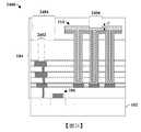
積體晶片200包括安置於基底102之上的介電結構104。介電結構104包括藉由多個蝕刻終止層204間隔開的多個堆疊的層間介電層202。在一些實施例中,多個堆疊的層間介電層202可包括二氧化矽(silicon dioxide)、經摻雜之二氧化矽(doped silicon dioxide)(例如摻碳二氧化矽(carbon doped silicon dioxide))、氮氧化矽(silicon oxynitride)、硼矽玻璃(borosilicate glass;BSG)、磷矽玻璃(phosphoric silicate glass;PSG)、硼磷矽玻璃(borophosphosilicate glass;BPSG)、氟化矽玻璃(fluorinated silicate glass;FSG)或類似者中的一或多者。在一些實施例中,多個蝕刻終止層204可包括碳化矽(silicon carbide)、氮化矽(silicon nitride)、氮化鈦(titanium nitride)、氮化鉭(tantalum nitride)或類似者。The integrated
多個導電內連線層108配置於介電結構104內。多個導電內連線層108包括具有多個內連線導線110及多個內連線通孔112的多個交替層,所述多個內連線導線110及所述多個內連線通孔112分別由多個層間介電層202中的一者包圍。舉例而言,第一內連線導線可由第一層間介電層包圍,第二內連線導線可由第二層間介電層包圍等。在一些實施例中,內連線導線110及內連線通孔112分別包括包圍金屬核芯(metal core)208的擴散障壁層206。在一些實施例中,擴散障壁層206可包括鉭、氮化鈦或類似者。在一些實施例中,金屬核芯208可包括銅、鎢、鋁或類似者。在一些實施例中,多個導電內連線層108中的一者可具有相對於外圍層間介電層(surrounding ILD layer)202的底部以第一角度α定向的側壁。在一些實施例中,第一角度α可為銳角。舉例而言,在一些實施例中,第一角度α可在80°與90°之間的範圍內。A plurality of
MIM電容器114亦配置於下部內連線層108a與上部內連線層108b之間的介電結構104內。MIM電容器114包含藉由電容器介電結構118與上部導電電極120間隔開的下部導電電極116。在一些實施例中,下部導電電極116具有處於電容器介電結構118下方的頂部表面,且電容器介電結構118具有處於上部導電電極120下方的頂部表面。在一些實施例中,下部內連線層108a及上部內連線層108b可包括金屬(例如銅、鎢、鋁或類似者)。在一些實施例中,下部導電電極116及上部導電電極120可包括與下部內連線層108a及/或上部內連線層108b的金屬不同的金屬。在一些實施例中,電容器介電結構118可包括高介電係數(high-k)介電材料。在一些實施例中,障壁層210(例如鈦、氮化鈦或類似者)可將下部導電電極116與介電結構104間隔開。在其他實施例中,障壁層210可省略。The
在一些實施例中,下部導電電極116可以第一距離d1延伸至下部內連線層108a的頂部表面下方。在一些實施例中,上部內連線層108b可以第二距離d2延伸至上部導電電極120的頂部表面下方。在一些實施例中,第二距離d2可大於第一距離d1。在一些實施例中,MIM電容器114的頂部表面(例如上部導電電極120的頂部表面)可為外圍層間介電層202的頂部表面下方的第三距離d3。在一些實施例中,上部內連線層108b可具有接觸上部導電電極120的內側壁的最外側壁。在其他實施例(未繪示)中,上部內連線層108b可橫向延伸至超出上部導電電極120的最外側壁。在此類實施例中,上部內連線層108b的內部側壁可接觸上部導電電極120的最外側壁。In some embodiments, the lower
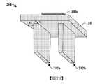
在一些實施例中,MIM電容器114可包含自MIM電容器114的下部表面向外延伸的一或多個第突出部212a-212b。在一些實施例中,一或多個第突出部212a-212b可分別具有高度h及寬度w。在一些實施例中,高度h與寬度w的比率可在大約1與大約50之間(例如1<h/w<50)的範圍內。在一些其他實施例中,高度h與寬度w的比率可在大約20與大約50之間(例如20<h/w<50)的範圍內。此類的高度h與寬度w之高比率於基底102的較小表面積上為MIM電容器114提供相對高的電容。In some embodiments, the
在圖2B的三維視圖214中繪示的一些實施例中,一或多個第突出部212a-212b可自下部導電電極116的最外側壁以非零距離來後置(移後(set-back))。舉例而言,在一些實施例中,第一突出部212a可透過第一後置(first set-back)s1自下部導電電極116的第一外側壁後置且透過第二後置(second set-back)s2自下部導電電極116的第二外側壁後置。In some embodiments depicted in the three-
一或多個第突出部212a-212b分別由自下部導電電極116的下部表面116L至下部導電電極116的底部向外延伸的下部側壁116s1限定。在一些實施例中,下部導電電極116的下部表面116L藉由層間介電層202與最接近的下伏蝕刻終止層204間隔開。在一些實施例中,下部導電電極116的下部側壁116s1可相對於外圍層間介電層202的底部以第二角度β定向。在一些實施例中,第二角度β可小於第一角度α。舉例而言,在一些實施例中,第二角度β可為在大約70°與大約90°之間的範圍內的銳角。在一些實施例中,下部導電電極116可更包括處於下部表面116L之上的上部側壁116s2。上部側壁116s2可相對於外圍層間介電層202的底部以第三角度γ定向。在一些實施例中,第三角度γ可為鈍角。舉例而言,在一些實施例中,第三角度γ可在大約90°與大約120°之間的範圍內。在一些實施例中,上部內連線層108b可包括相對於上部導電電極120的頂部以第四角度δ定向的側壁。在一些實施例中,第四角度δ可為在80°與90°之間的範圍內的銳角。在一些實施例中,第一角度α可實質上等於第四角度δ。The one or more
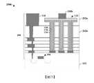
圖3示出具有垂直地延伸於多個導電內連線層之上的高密度MIM電容器的積體晶片300的一些其他實施例的橫截面圖。FIG. 3 shows a cross-sectional view of some other embodiments of an
積體晶片300包括配置於基底102之上的介電結構104內的MIM電容器114。MIM電容器114具有藉由電容器介電結構118與上部導電電極120間隔開的下部導電電極116。The
在一些實施例中,下部導電電極116將電容器介電結構118的最外側壁與介電結構104橫向間隔開,且電容器介電結構118將上部導電電極120的最外側壁與介電結構104橫向間隔開。在一些此類實施例中,下部導電電極116的最外側壁可相對於外圍層間介電層202的底部以角度α定向。角度α可為銳角(例如在大約70°與大約90°之間的範圍內)。在一些實施例中,下部導電電極116、電容器介電結構118以及上部導電電極120的頂部表面直接接觸MIM電容器114之上的蝕刻終止層204。In some embodiments, the lower
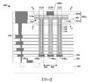
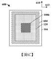
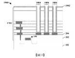
圖4A至圖4C示出具有高密度MIM電容器的積體晶片的一些其他實施例。圖4A示出積體晶片的橫截面圖400。圖4B示出積體晶片沿橫截面圖400的橫截面線A-A'的俯視圖406。圖4C示出積體晶片沿橫截面圖400的橫截面線B-B'的俯視圖408。4A to 4C show some other embodiments of integrated wafers with high-density MIM capacitors. FIG. 4A shows a
如橫截面圖400中所繪示,積體晶片包括MIM電容器114,所述MIM電容器114配置於基底102之上的介電結構104內且具有藉由電容器介電結構118與上部導電電極120間隔開的下部導電電極116。在一些實施例中,MIM電容器114可延伸至上部層間介電層202u。上部層間介電層202u可包括沿接縫(seam)203接觸第二層間介電層202b的第一層間介電層202a,所述接縫沿MIM電容器114的下部表面114L延行(延伸)且與內連線導線110a的側壁相交。在各種實施例中,第一層間介電層202a及第二層間介電層202b可包括相同介電材料或不同介電材料。As depicted in the
MIM電容器114包含自MIM電容器114的下部表面114L向外延伸的多個突出部212a-212c。多個突出部212a-212c自MIM電容器114的下部表面114L垂直地延伸至多個下部內連線結構108a1-108a3。在一些實施例中,多個下部內連線結構108a1-108a3可藉由介電結構104彼此橫向間隔開。在其他實施例(未繪示)中,多個突出部212a-212c可自MIM電容器114的下部表面114L向外延伸至單個下部內連線結構,所述下部內連線結構持續延伸於多個突出部212a-212c下方。The
多個突出部212a-212c透過由介電結構104彼此間隔開的多個側壁而限定。舉例而言,第一突出部212a的側壁可藉由一或多個層間介電層202及藉由一或多個蝕刻終止層204與第二突出部212b的側壁橫向間隔開。在一些實施例中,多個突出部212a-212c可透過間距402配置並間隔距離404。在一些實施例中,間距402可在大約0.1微米與大約1微米之間的範圍內。在一些實施例中,距離404可在大約0.05微米與大約0.5微米之間的範圍內。在形成MIM電容器114期間,小於大約0.05微米的距離404可導致介電結構104皺縮(collapse)(例如介電結構彎曲至相鄰側壁中),而大於大約0.5微米的距離404縮減MIM電容器114針對基底102之給定表面積的電容。The plurality of
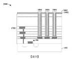
圖5A至圖5C示出具有高密度MIM電容器的積體晶片的一些其他實施例。圖5A示出積體晶片的橫截面圖500。圖5B示出積體晶片沿橫截面圖500的橫截面線A-A'的俯視圖504。圖5C示出積體晶片沿橫截面圖500的橫截面線B-B'的俯視圖506。5A to 5C show some other embodiments of integrated wafers with high-density MIM capacitors. FIG. 5A shows a
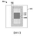
如圖5A的橫截面圖500中所繪示,積體晶片包括MIM電容器114,所述MIM電容器114配置於基底102之上的介電結構104內且具有藉由電容器介電結構118與上部導電電極120間隔開的下部導電電極116。在一些實施例中,上部導電電極120以非零距離502自下部導電電極116及電容器介電結構118的最外側壁來橫向後置。在一些實施例中,非零距離502可在大約0微米與大約0.5微米之間的範圍內。As shown in the
在一些實施例中,下部導電電極116及上部導電電極120可包括相同材料。在其他實施例中,下部導電電極116可包括與上部導電電極120不同的材料。在一些實施例中,下部導電電極116及/或上部導電電極120可包括鈦、氮化鈦、鉭、氮化鉭、鉭矽氮化物(tantalum silicon nitride)、鈦矽氮化物(titanium silicon nitride)、氮化鎢(例如WN、WN2)、鎢矽氮化物(tungsten silicon nitride)、鈦鋁、銅、鋁、鈷、釕、銥、氧化銥、鉑、鎢或類似者。在一些實施例中,下部導電電極116可具有在大約0.005微米與大約0.50微米之間的範圍內的第一厚度t1。在一些實施例中,上部導電電極120可具有在大約0.005微米與大約0.50微米之間的範圍內的第三厚度t3。在一些實施例中,上部導電電極120可比下部導電電極116具有更大高度。In some embodiments, the lower
在一些實施例中,電容器介電結構118可包括氧化物、high-k介電材料或類似者。舉例而言,在各種實施例中,電容器介電結構118可包括二氧化矽、氮化矽(例如Si3N4)、氧化鉭(例如Ta2O5)、氧化鋁(例如Al2O3)、氧化鑭(例如La2O3)、氧化鉿(例如HfO2)、氧化鋯(例如ZrO2)、鋯鋁氧化物(例如ZrAlxOy)、鉿鋁氧化物(例如HfAlxOy)、溴鈦氧化物(例如BrTiO2)、鍶鈦氧化物(例如SrTiO2、SrTiO3)或類似者中的一或多者。在一些實施例中,電容器介電結構118可具有在大約0.001微米與大約0.30微米之間的範圍內的第二厚度t2。In some embodiments, the
應瞭解,在各種實施例中,電容器介電結構(例如電容器介電結構118)可包括單個介電層或多個堆疊的介電層。圖6A至圖7D示出包括多層的電容器介電結構的一些例示性實施例。在電容器介電結構內使用多個膜層可增大MIM電容器的崩潰電壓(breakdown voltage)。應瞭解,圖6A至圖7D中示出的實施例非旨於限制,而是僅僅作為所揭露的電容器介電結構的多種實例。It should be appreciated that in various embodiments, the capacitor dielectric structure (eg, capacitor dielectric structure 118) may include a single dielectric layer or multiple stacked dielectric layers. 6A to 7D show some exemplary embodiments of capacitor dielectric structures including multiple layers. The use of multiple film layers within the capacitor dielectric structure can increase the breakdown voltage of the MIM capacitor. It should be understood that the embodiments shown in FIGS. 6A to 7D are not intended to be limiting, but merely as various examples of the disclosed capacitor dielectric structure.
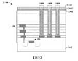
圖6A至圖6C示出具有包括多層電容器介電結構的高密度MIM電容器的積體晶片的一些實施例。圖6A示出積體晶片的橫截面圖600。圖6B示出積體晶片沿橫截面圖600的橫截面線A-A'的俯視圖606。圖6C示出積體晶片沿橫截面圖600的橫截面線B-B'的俯視圖608。6A to 6C show some embodiments of an integrated wafer having a high-density MIM capacitor including a multilayer capacitor dielectric structure. FIG. 6A shows a
如橫截面圖600中所繪示,積體晶片包括配置於基底102之上的介電結構104內的MIM電容器114。MIM電容器114具有藉由多層電容器介電結構601與上部導電電極120間隔開的下部導電電極116。在一些實施例中,多層電容器介電結構601可包括第一介電層602及第一介電層602之上的第二介電層604。在一些實施例中,第一介電層602可包括第一介電材料,且第二介電層604可包括與第一介電材料不同的第二介電材料。舉例而言,在一些實施例中,第一介電層602可包括第一high-k介電材料(例如氮化鉭、氧化鋁或類似者),且第二介電層604可包括第二high-k介電材料(例如氧化鉿、氧化鋯或類似者)。在其他實施例中,第一介電層602可包括high-k介電材料,且第二介電層604可包括具有小於或等於二氧化矽的介電常數之介電常數的介電材料,或第一介電層602可包括具有小於或等於二氧化矽之介電常數的介電常數的介電材料,第二介電層604可包括high-k介電材料。As depicted in the
如俯視圖606中所繪示,第一介電層602及第二介電層604完全包圍自MIM電容器114的下部表面向外延伸的多個突出部212a-212c內的上部導電電極120。在一些實施例中,如俯視圖608中所繪示,第二介電層604可沿第一方向610橫向延伸超出上部導電電極120且亦沿與所述第一方向610垂直的第二方向612延伸超出上部導電電極120。As depicted in the
圖7A至圖7D示出具有包括多層之電容器介電結構的高密度MIM電容器的積體晶片的一些其他實施例的橫截面圖。7A to 7D show cross-sectional views of some other embodiments of an integrated wafer of a high-density MIM capacitor having a capacitor dielectric structure including multiple layers.
圖7A的橫截面圖700示出包含多層電容器介電結構701的MIM電容器114的一些實施例,所述多層電容器介電結構701包括相同介電材料的多個層702a-702c。在一些實施例中,多層電容器介電結構701可包括第一介電材料的第一層702a、第一介電材料的第二層702b以及第一介電材料的第三層702c。相同介電材料的多個層702a-702c可藉由不同(即,單獨)的沉積製程形成,且因此可沿著多個層702a至層702c之間可見的邊界(例如接縫)而間隔開。相同介電材料的多個層702a-702c的使用可改良多層電容器介電結構701的品質,從而改良MIM電容器的電特性。The
圖7B的橫截面圖704示出包含多層電容器介電結構703的MIM電容器114的一些替代實施例,所述多層電容器介電結構703包括具有兩種不同介電材料的多個層706a-706c。在一些實施例中,多層電容器介電結構703可包括第一介電材料的第一層706a,所述第一層706a具有接觸下部導電電極116的下部表面及外部側壁。多層電容器介電結構703可更包括第二介電材料的第二層706b,所述第二層706b具有接觸第一層706a的下部表面及外部側壁。多層電容器介電結構703可更包括第一介電材料的第三層706c,所述第三層706c具有接觸第二層706b的下部表面及外部側壁並具有接觸上部導電電極120的上部表面及內部側壁。在一些實施例中,第一介電材料及第二介電材料可包括不同介電材料。使第一層706a及第三層706c接觸第二層706b的相對側可實現所述膜層之間的較佳介面特性,且因此改良多層電容器介電結構703的品質。The
圖7C的橫截面圖708示出包含多層電容器介電結構709的MIM電容器114的一些替代實施例,所述多層電容器介電結構709包括具有三種不同介電材料的多個層710a-710d。在一些實施例中,多層電容器介電結構709可包括第一介電材料的第一層710a、第二介電材料的第二層710b、第三介電材料的第三層710c、及第一介電材料的第四層710d。第一層710a具有接觸下部導電電極116的下部表面及外部側壁。第二層710b具有接觸第一層710a的下部表面及外部側壁。第二層710b更包括接觸第三介電材料的第三層710c的上部表面及內部側壁。第三層710c具有接觸第一介電材料的第四層710d的上部表面及內部側壁。第四層710d更包括接觸上部導電電極120的上部表面及內部側壁。在一些實施例中,第一介電材料、第二介電材料以及第三介電材料可包括不同介電材料。The
圖7D的橫截面圖712示出包含多層電容器介電結構713的MIM電容器114的一些替代實施例,所述多層電容器介電結構713包括以週期性重複圖案配置的介電材料的多個層。在一些實施例中,多層電容器介電結構713可包括第一介電材料第一層714a、第二介電材料的第二層714b、第一介電材料的第三層714c、及第二介電材料的第四層714d。第一層714a具有接觸下部導電電極116的下部表面及外部側壁。第二層714b具有接觸第一層714a的下部表面及外部側壁。第二層714b包括接觸第一介電材料的第三層714c的上部表面及內部側壁。第三層714c包括接觸第二介電材料的第四層714d的上部表面及內部側壁。第四層714d包括接觸上部導電電極120的上部表面及內部側壁。在一些實施例中,第一介電材料及第二介電材料可包括不同介電材料。The
圖8示出具有高密度MIM電容器的積體晶片800的一些其他實施例的橫截面圖。8 shows a cross-sectional view of some other embodiments of an
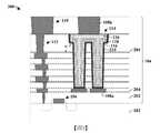
積體晶片800包括配置於基底102內的電晶體元件106。電晶體元件106耦接至由基底102之上的介電結構104所包圍的多個導電內連線層108。接合襯墊(bond pad)804配置於介電結構104之上。接合襯墊804配置至多個導電內連線層108的最頂部內連線導線110u上。第一鈍化層806配置於介電結構104及接合襯墊804之上。在一些實施例中,第一鈍化層806可包括氧化物(例如二氧化矽)、氮化物(例如氮氧化矽)、碳化物(例如碳化矽)或類似者。第二鈍化層808配置於第一鈍化層806及接合襯墊804上。在一些實施例中,第二鈍化層808例如可包括聚合物,諸如聚醯亞胺(polyimide)。重佈線層810配置於第一鈍化層806之上,且將接合襯墊804電性耦接至上覆的凸塊下金屬(under bump metallurgy;UBM)層814及電性耦接至於UBM層814之上的焊料球816。第三鈍化層812配置於第二鈍化層808及重佈線層810之上。第三鈍化層812橫向地圍繞UBM層814。The
電晶體元件802亦在由介電結構104所包圍的MIM電容器114正下方的位置處配置於基底102內。在一些實施例中,電晶體元件802可包括主動元件(例如電性耦接至具有邏輯功能性的電路內的其他元件的所述主動元件),而在其他實施例中,電晶體元件802可包括虛設元件(例如並未電性耦接至具有邏輯功能性的電路內的其他元件的所述虛設元件)。電晶體元件802包括閘極電極802a,所述閘極電極802a藉由閘極介電層802b與基底102間隔開。閘極電極802a橫向地安置於基底102內並於源極區802s與汲極區802d之間。The
MIM電容器114包括自MIM電容器114的下部表面向外延伸以接觸閘極電極802a的上部表面的多個突出部212a-212c。舉例而言,多個突出部212a-212c由自MIM電容器114的下部表面垂直地延伸至閘極電極802a的上部表面的側壁來限定。在一些實施例中,閘極電極802a可比電晶體元件106的閘極電極具有更大寬度,以使得多個突出部212a-212c可接觸閘極電極802a。在一些實施例中,MIM電容器114具有沿著水平平面818配置的最上部表面114u,所述最上部表面114u與最頂部內連線導線110u相交。藉由使MIM電容器114自閘極電極802a延伸至鄰近於最頂部內連線導線110u的豎直位置,MIM電容器114能夠在佔用基底102的相對較小的表面積時實現較大電容。此外,藉由將MIM電容器114連接至主動電晶體元件的閘極電極802a,MIM電容器114可用於電佈線(例如代替導電內連線導線及/或通孔)。The
圖9示出具有高密度MIM電容器的積體晶片900的一些其他實施例的橫截面圖。9 shows a cross-sectional view of some other embodiments of an
積體晶片900包括在由介電結構104所包圍的MIM電容器114正下方的位置處配置於基底102內的電晶體元件902。電晶體元件902包括藉由閘極介電層902b與基底102間隔開的閘極電極902a。閘極電極902a橫向地安置於基底102內的源極區902s與汲極區902d之間。在一些實施例中,源極區902s可比汲極區902d具有更大寬度,或汲極區902d可比源極區902s具有更大寬度。在一些實施例中,MIM電容器114包括自MIM電容器114的下部表面向外延伸以接觸源極區902s的多個突出部212a-212c。在一些實施例中,MIM電容器114具有沿著水平平面818配置的最上部表面114u,所述最上部表面114u與最頂部內連線導線110u相交。藉由使多個突出部212a-212c自源極區902s垂直地延伸至鄰近於最頂部內連線導線110u的豎直位置,MIM電容器114能夠在佔用基底102的相對較小的表面積時實現較大電容。The
圖10示出具有高密度MIM電容器的積體晶片1000的一些其他實施例的橫截面圖。10 shows a cross-sectional view of some other embodiments of an
積體晶片1000包括配置於基底102內的電晶體元件106。電晶體元件106耦接至由基底102之上的介電結構104所包圍的多個導電內連線層108。多個導電內連線層108包括多個內連線導線110及多個內連線通孔112。MIM電容器114垂直地配置於下部內連線層108a與上部內連線層108b之間。MIM電容器114的頂部表面沿與內連線通孔112中的一者的側壁相交的水平平面1002延伸。The
圖11示出具有高密度MIM電容器的積體晶片1100的一些其他實施例的橫截面圖。11 shows a cross-sectional view of some other embodiments of an
積體晶片1100包括由基底102之上的介電結構104所包圍的MIM電容器114。MIM電容器114包括自MIM電容器114的下部表面向外延伸的多個突出部1102a-1102c。多個突出部1102a-1102c具有不同高度且延伸至基底102之上的不同豎直位置。舉例而言,多個突出部1102a -1102c可包括具有第一高度h1的第一突出部1102a、具有第二高度h2的第二突出部1102b以及具有第三高度h3的第三突出部1102c。在一些實施例中,第一突出部1102a具有接觸安置於介電結構104內的下部內連線層108a(例如導電內連線導線)的底部表面。在一些實施例中,第二突出部1102b具有接觸電晶體元件802的閘極電極802a的底部表面。在一些實施例中,第三突出部1102c具有接觸電晶體元件902的源極區902s的底部表面。The
圖12示出具有高密度MIM電容器的積體晶片1200的一些其他實施例的橫截面圖。FIG. 12 shows a cross-sectional view of some other embodiments of an
積體晶片1200包括在由介電結構104所包圍的MIM電容器114正下方的位置處配置於基底102內的電晶體元件1202。電晶體元件1202包括藉由閘極介電層1202b與基底102間隔開的閘極電極1202a。閘極電極1202a橫向地安置於基底102內的源極區1202s與汲極區1202d之間。在一些實施例中,源極區1202s可比汲極區1202d具有更大寬度。MIM電容器114包括自MIM電容器114的下部表面向外延伸至處於源極區1202s內(即,由源極區1202s橫向包圍)的位置的多個突出部212a-212c。藉由使多個突出部212a-212c垂直地延伸至源極區1202s內,MIM電容器114能夠在佔用基底102的相對較小的表面積時實現較大電容。The
雖然圖9以及圖11至圖12示出具有接觸源極區的一或多個突出部的MIM電容器,但應瞭解,在其他實施例中,一或多個突出部可自MIM電容器的下部表面向外延伸以接觸汲極區。使多個突出部延伸至源極區、汲極區及/或閘極電極,使得MIM電容器可用於佈線(例如代替內連線導線/通孔),且因此增強佈局靈活性及/或縮減導電內連線佈線所使用的面積。Although FIGS. 9 and 11 to 12 show MIM capacitors having one or more protrusions that contact the source region, it should be understood that in other embodiments, one or more protrusions may be from the lower surface of the MIM capacitor Extend outward to contact the drain region. Extend multiple protrusions to the source region, the drain region, and/or the gate electrode so that the MIM capacitor can be used for wiring (eg, instead of interconnect wires/vias), and thus enhance layout flexibility and/or reduce conduction The area used for interconnection wiring.
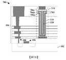
圖13A示出具有高密度MIM電容器的積體晶片1300的一些其他實施例的橫截面圖。圖13B示出圖13A的積體晶片1300的示意圖1306。13A shows a cross-sectional view of some other embodiments of an
如圖13A的橫截面圖中所繪示,積體晶片1300具有包括安置於下部導電電極116與上部導電電極120之間的電容器介電結構118的MIM電容器114。下部導電電極116耦接至第一電晶體1302,且上部導電電極120耦接至第二電晶體1304。在操作期間,第一電晶體1302可將第一電壓V1施加至下部導電電極116,而第二電晶體1304可將第二電壓V2施加至上部導電電極120。MIM電容器114具有電容CMIM且將儲存與下部導電電極116及上部導電電極120的表面積成比例的能量。As depicted in the cross-sectional view of FIG. 13A, the
圖14示出具有垂直地延伸於多個導電內連線層之上的高密度MIM電容器的三維積體晶片(three-dimensional integrated chip;3DIC)1400的一些其他實施例。FIG. 14 shows some other embodiments of a three-dimensional integrated chip (3DIC) 1400 with a high-density MIM capacitor that extends vertically over a plurality of conductive interconnect layers.
三維積體晶片1400包括第一積體電路(integrated circuit; IC)晶粒1402a及堆疊至第一IC晶粒1402a上的第二IC晶粒1402b。第一IC晶粒1402a包括第一基底102a及第一基底102a上的第一介電結構104a。第二IC晶粒1402b包括第二基底102b及第二基底102b上的第二介電結構104b。第一IC晶粒1402a沿混合接合介面區(hybrid bonding interface region)1404耦接至第二IC晶粒1402b。在一些實施例中,混合接合介面區1404包括包圍第一導電接合結構1408a的第一介電接合層1406a及包圍第二導電接合結構1408b的第二介電接合層1406b。在一些實施例中,第一介電接合層1406a及第二介電接合層1406b可包括氧化物、氮化物或類似者。在一些實施例中,第一導電接合結構1408a及第二導電接合結構1408b可包括鋁、銅或類似者。The three-dimensional
MIM電容器114配置於第一介電結構104a內。MIM電容器114包括安置於下部導電電極116與上部導電電極120之間的電容器介電結構118。下部導電電極116耦接至第一基底102a內的第一電晶體1302。上部導電電極120耦接至第二基底102b內的第二電晶體1304。在操作期間,第一電晶體1302可將第一電壓V1施加至下部導電電極116,而第二電晶體1304可將第二電壓V2施加至上部導電電極120。The
圖15示出具有垂直地延伸於多個導電內連線層之上的高密度MIM電容器的三維積體晶片1500的一些其他實施例。FIG. 15 illustrates some other embodiments of a three-dimensional
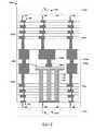
三維積體晶片 1500包括第一IC晶粒1402a及堆疊至第一IC晶粒1402a上的第二IC晶粒1402b。第一IC晶粒1402a包括第一基底102a及第一基底102a上的第一介電結構104a。第二IC晶粒1402b包括第二基底102b及第二基底102b上的第二介電結構104b。第一IC晶粒1402a沿混合接合介面區1404耦接至第二IC晶粒1402b。The three-dimensional
第一MIM電容器114a配置於第一介電結構104a內。第一MIM電容器114a包括安置於第一導電電極116a與第二導電電極120a之間的第一介電結構118a。第一導電電極116a耦接至第一基底102a內的第一電晶體1302。第二導電電極120a耦接至配置於第二介電結構104b內的第二MIM電容器114b。第二MIM電容器114b包括安置於第三導電電極116b與第四導電電極120b之間的第二介電結構118b。第三導電電極116b耦接至第二基底102b內的第二電晶體1304。在操作期間,第一電晶體1302可將第一電壓V1施加至第一導電電極116a,而第二電晶體1304可將第二電壓V2施加至第三導電電極116b。The
圖16至圖25示出形成具有垂直地延伸於多個導電內連線層之上的高密度MIM電容器的積體晶片的方法的一些實施例的橫截面圖1600至橫截面圖2500。雖然參考方法描述了圖16至圖25,但應瞭解,圖16至圖25中所揭露的結構不限於此類方法,而反而可單獨作為獨立於所述方法的結構。FIGS. 16-25 illustrate
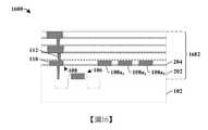
如圖16的橫截面圖1600中所繪示,多個導電內連線層108形成於基底102之上的第一介電結構1602內。在一些實施例中,第一介電結構1602可包括由多個蝕刻終止層204間隔開的多個堆疊的層間介電層202。在一些實施例中,多個導電內連線層108分別包括耦接至形成於基底102內的電晶體元件106的內連線導線110及內連線通孔112。在一些實施例中,多個導電內連線層108可更包括具有一或多個下部內連線結構108a1-108a3的下部內連線層,所述下部內連線結構108a1-108a3自多個導電內連線層108橫向偏移。在一些實施例中,多個導電內連線層108及/或一或多個下部內連線結構108a1-108a3可分別藉由鑲嵌製程(damascene process)形成。在此類實施例中,層間介電層202形成於基底102之上。層間介電層202隨後經蝕刻以形成介層窗孔及/或溝渠,所述介層窗孔及/或溝渠經導電材料(例如鎢、銅及/或鋁)填充。隨後執行化學機械平坦化(chemical mechanical planarization;CMP)製程以自層間介電層202之上移除過量的導電材料。As shown in the
如圖17的橫截面圖1700中所繪示,一或多個額外的層間介電層1701及層間介電層202a形成於基底102之上以限定第二介電結構1702。在一些實施例中,一或多個額外的層間介電層1701及層間介電層202a藉由沉積製程(例如化學氣相沉積(chemical vapor deposition;CVD)、電漿增強型化學氣相沉積(plasma enhanced chemical vapor deposition;PE-CVD)、原子層沉積(atomic layer deposition;ALD)、物理氣相沉積(physical vapor deposition;PVD)等)形成。在一些實施例中,一或多個蝕刻終止層204a可形成於一或多個額外的層間介電層1701與層間介電層202a之間。As depicted in the
第一經圖案化罩幕層1704形成於一或多個額外的層間介電層1701及層間介電層202a之上。在一些實施例中,第一經圖案化罩幕層1704可包括硬式罩幕,所述硬式罩幕包括鈦、碳化矽、氮氧化矽、鉭或類似者。在此類實施例中,第一經圖案化罩幕層1704可沉積於第二介電結構1702之上,且隨後使用微影製程圖案化以形成限定暴露第二介電結構1702的上部表面的一或多個開口1706的側壁。開口1706可位於一或多個下部內連線結構108a1-108a3的正上方。在其他實施例中,第一經圖案化罩幕層1704可包括光阻。The first
如圖18的橫截面圖1800中所繪示,對第二介電結構1702執行第一蝕刻製程以限定(定義)延伸至第二介電結構1702中的一或多個溝渠1804。一或多個溝渠1804自第二介電結構1702的上部表面垂直地延伸超出多個導電內連線層108中的兩者或多於兩者,直至一或多個下部內連線結構108a1-108a3。在一些實施例中,藉由根據第一經圖案化罩幕層1704使第二介電結構1702暴露於一或多種第一蝕刻劑1802來執行第一蝕刻製程。在一些實施例中,一或多種第一蝕刻劑1802可包括乾式蝕刻劑。在一些實施例中,乾式蝕刻劑可具有蝕刻化學物質,所述蝕刻化學物質包括氧(O2)、氮(N2)、氫(H2)、氬(Ar)及/或氟物種(例如,CF4、CHF3、C4F8等)中的一或多者。As depicted in the
如圖19的橫截面圖1900中所繪示,下部導電電極層1902沿限定一或多個溝渠1804的第二介電結構1702的側壁及下部表面形成。在各種實施例中,下部導電電極層1902可包括鈦、氮化鈦、鉭、氮化鉭、鉭矽氮化物、鈦矽氮化物、氮化鎢(例如WN、WN2)、鎢矽氮化物、鈦鋁、銅、鋁、鈷、釕、銥、氧化銥、鉑、鎢或類似者。在一些實施例中,下部導電電極層1902可藉由共形沉積製程(conformal deposition process)形成。舉例而言,在各種實施例中,下部導電電極層1902可藉由ALD製程、CVD製程或PVD製程形成。As depicted in the
如圖20的橫截面圖2000中所繪示,一或多個介電層2002形成於一或多個溝渠1804內且沿下部導電電極層1902的側壁及下部表面形成。在各種實施例中,一或多個介電層2002可包括二氧化矽、氮化矽(例如Si3N4)、氧化鉭(例如Ta2O5)、氧化鋁(例如Al2O3)、氧化鑭(例如La2O3)、氧化鉿(例如HfO2)、氧化鋯(例如ZrO2)、鋯鋁氧化物(例如ZrAlxOy)、鉿鋁氧化物(例如HfAlxOy)、溴鈦氧化物(例如BrTiO2)、鍶鈦氧化物(例如SrTiO2、SrTiO3)或類似者中的一或多者。在一些實施例中,一或多個介電層2002可藉由共形沉積製程(例如ALD製程、CVD製程或PVD製程)形成。As depicted in the
如圖21的橫截面圖2100中所繪示,上部導電電極層2102形成於一或多個溝渠1804內且沿一或多個介電層2002的側壁及下部表面形成。在各種實施例中,上部導電電極層2102可包括鈦、氮化鈦、鉭、氮化鉭、鉭矽氮化物、鈦矽氮化物、氮化鎢(例如WN、WN2)、鎢矽氮化物、鈦鋁、銅、鋁、鈷、釕、銥、氧化銥、鉑、鎢或類似者。在一些實施例中,上部導電電極層2102可藉由共形沉積製程形成。舉例而言,在各種實施例中,上部導電電極層2102可藉由ALD製程、CVD製程或PVD製程形成。As shown in the
圖22A至圖22B示出繪示可用於使上部導電電極層(圖21的上部導電電極層2102)、一或多個介電層(圖21的介電層2002)以及下部導電電極層(圖21的下部導電電極層1902)圖案化以限定MIM電容器114的不同圖案化製程的一些實施例的橫截面圖。FIGS. 22A to 22B show the upper conductive electrode layer (upper
在圖22A的橫截面圖2200中繪示的一些實施例中,第二經圖案化罩幕層2202形成於上部導電電極層(圖21的上部導電電極層2102)上。根據第二經圖案化罩幕層2202對上部導電電極層(圖21的上部導電電極層2102)執行第二蝕刻製程以移除未經第二經圖案化罩幕層2202覆蓋的區域中的上部導電電極層(圖21的上部導電電極層2102)並定義出上部導電電極120。在一些實施例中,可藉由使在未經第二經圖案化罩幕層2202覆蓋的區域中的上部導電電極層(圖21的上部導電電極層2102)暴露於一或多種第二蝕刻劑2204來執行第二蝕刻製程。在一些實施例中,第二經圖案化罩幕層2202可包括光阻。In some embodiments depicted in the
如橫截面圖2206中所繪示,第三經圖案化罩幕層2208隨後形成至上部導電電極120及一或多個介電層(橫截面圖2200的介電層2002)上。隨後根據第三圖案化罩幕層2208對一或多個介電層(橫截面圖2200的介電層2002)及下部導電電極層(橫截面圖2200的下部導電電極層1902)執行第三蝕刻製程以定義電容器介電結構118及下部導電電極116。第三蝕刻製程移除未經第三經圖案化罩幕層2208覆蓋的區域中的一或多個介電層(橫截面圖2200的介電層2002)及下部導電電極層(橫截面圖2200的下部導電電極層1902)。在一些實施例中,可藉由使在未經第三經圖案化罩幕層2208覆蓋的區域中的一或多個介電層(橫截面圖2200的介電層2002)及下部導電電極層(橫截面圖2200的下部導電電極層1902)暴露於一或多種第三蝕刻劑2210來執行第三蝕刻製程。在一些實施例中,第三經圖案化罩幕層2208可包括光阻。As depicted in
在圖22B的橫截面圖2212繪示的一些替代實施例中,第四經圖案化罩幕層2214形成於上部導電電極層(圖21的上部導電電極層2102)上。根據第四經圖案化罩幕層2214對上部導電電極層(圖21的上部導電電極層2102)、一或多個介電層(圖21的介電層2002)以及下部導電電極層(圖21的下部導電電極層1902)執行第四蝕刻製程。第四蝕刻製程定義上部導電電極120、電容器介電結構118以及下部導電電極116。在一些實施例中,可藉由使在未經第四經圖案化罩幕層2214覆蓋的區域中的上部導電電極層(圖21的上部導電電極層2102)、一或多個介電層(圖21的介電層2002)以及下部導電電極層(圖21的下部導電電極層1902)暴露於一或多種第四蝕刻劑2216來執行第四蝕刻製程。在一些實施例中,第四經圖案化罩幕層2214可包括光阻。In some alternative embodiments depicted in the
如圖23的橫截面圖2300中所繪示,第二層間介電層202b形成於第二介電結構(圖22A的第二介電結構1702)之上以限定(定義)介電結構104。在一些實施例中,第二層間介電層202b可包括與下伏第一層間介電層202a相同的材料。第一層間介電層202a與第二層間介電層202b形成自MIM電容器114下方持續延伸至MIM電容器114之上的上部層間介電層202u。在各種實施例中,第二層間介電層202b可包括介電材料,諸如氧化物、氮化物或類似者。在一些實施例中,第二層間介電層202b可藉由ALD製程、CVD製程或PVD製程形成。As shown in the
如圖24的橫截面圖2400中所繪示,對介電結構104執行第五蝕刻製程。第五蝕刻製程限定介層窗孔2402及內連線導線溝渠2404,所述介層窗孔2402及內連線導線溝渠2404自介電結構104的頂部表面垂直地延伸至MIM電容器114的頂部下方的位置。第五蝕刻製程進一步限定MIM電容器114正上方的上部內連線層開口2406。在一些實施例中,上部內連線層開口2406可以以距離d延伸至MIM電容器114的頂部表面(例如上部導電電極120的頂部表面)下方。在此類實施例中,上部內連線層開口2406可由介電結構104及上部導電電極120二者的側壁限定。在一些實施例中,可藉由根據第五經圖案化罩幕層使介電結構104選擇性地暴露於第五蝕刻劑來執行第五蝕刻製程。As shown in the
如圖25的橫截面圖2500中所繪示,一或多種導電材料形成於介層窗孔(例如圖24的介層窗孔2402)、內連線導線溝渠(圖24的內連線導線溝渠2404)以及上部內連線層開口(例如圖24的上部內連線層開口2406)內。在一些實施例中,可使用沉積製程及/或鍍覆製程(例如電鍍、無電式鍍覆等)來形成一或多種導電材料。在各種實施例中,一或多種導電材料可包括鎢、銅、鋁或類似者。在一些實施例中,可在形成一或多種導電材料之後執行平坦化製程(例如化學機械平坦化(CMP)製程)以自介電結構104之上移除過量的一或多種導電材料,且以限定(定義)內連線導線110及上部內連線層108b。As shown in the
圖26示出形成具有垂直地延伸於多個導電內連線層之上的高密度MIM電容器的積體晶片的方法2600的一些實施例的流程圖。26 shows a flowchart of some embodiments of a
儘管在本文中之方法2600經說明且描述為一系列動作或事件,但應瞭解,不應以限制性意義來解譯此類動作或事件的所說明之次序。舉例而言,除本文中所說明及/或所描述的動作或事件之外,一些動作可與其他動作或事件以不同次序及/或同時出現。此外,可能需要並非所有的所示出動作來實施本文中所描述的一或多個態樣或實施例。另外,本文中所描繪的動作中的一或多者可以一或多個單獨動作及/或階段進行。Although the
在動作2602中,多個導電內連線層形成於基底之上的第一介電結構內。圖16示出與動作2602對應的一些實施例的橫截面圖1600。In
在動作2604中,一或多個額外層間介電層形成於第一介電結構之上以限定第二介電結構。圖17示出與動作2604對應的一些實施例的橫截面圖1700。In
在動作2606中,選擇性地蝕刻第二介電結構以限定垂直地延伸穿過第二介電結構直至超出兩個或大於兩個導電內連線層的一或多個溝渠。圖18示出與動作2606對應的一些實施例的橫截面圖1800。In
在動作2608中,下部導電電極層形成於一或多個溝渠內。圖19示出與動作2608對應的一些實施例的橫截面圖1900。In
在動作2610中,一或多個介電層形成於下部導電電極層之上的一或多個溝渠內。圖20示出與動作2610對應的一些實施例的橫截面圖2000。In
在動作2612中,上部導電電極層形成於一或多個介電層之上的一或多個溝渠內。圖21示出與動作2612對應的一些實施例的橫截面圖2100。In
在動作2614中,選擇性地蝕刻下部導電電極層、一或多個介電層以及上部導電電極層以限定MIM電容器。圖22A示出與動作2614對應的一些實施例的橫截面圖2200。圖22B示出與動作2614對應的一些替代實施例的橫截面圖2200。In
在動作2616中,層間介電層形成於MIM電容器之上。圖23示出與動作2616對應的一些替代實施例的橫截面圖2300。In
在動作2618中,上部內連線層形成於處於橫向鄰近於MIM電容器的位置處且垂直地位於MIM電容器之上的位置處的層間介電層內。圖24至圖25示出與動作2618對應的一些替代實施例的橫截面圖2400與橫截面圖2500。In
因此,在一些實施例中,本揭露內容是關於一種高密度MIM(金屬-絕緣體-金屬)電容器,所述高密度MIM電容器垂直地延伸於多個導電內連線層之上以使得能夠在相對較小的面積上實現高電容。Therefore, in some embodiments, the disclosure relates to a high-density MIM (metal-insulator-metal) capacitor that extends vertically over a plurality of conductive interconnect layers to enable High capacitance is achieved on a small area.
在一些實施例中,本揭露內容是關於一種積體晶片。所述積體晶片包含:介電結構,安置於基底之上;多個導電內連線層,配置於所述介電結構內,其中所述多個導電內連線層包括具有多個內連線導線及多個內連線通孔的多個交替層;以及金屬-絕緣體-金屬電容器,配置於所述介電結構內且包括透過電容器介電結構與上部導電電極間隔開的下部導電電極,其中所述金屬-絕緣體-金屬電容器垂直地延伸超出所述多個導電內連線層中的兩者或多於兩者。在一些實施例中,所述下部導電電極具有在所述下部導電電極的最底部表面與所述下部導電電極的下部表面之間垂直地延伸的多個側壁,所述下部表面面朝所述基底。在一些實施例中,所述下部導電電極的所述下部表面以非零距離與最接近的下伏之蝕刻終止層間隔開。在一些實施例中,所述介電結構包括層間介電層,所述層間介電層自所述下部表面正下方持續延伸至所述上部導電電極正上方。在一些實施例中,所述下部導電電極自橫向地包圍所述金屬-絕緣體-金屬電容器的層間介電層的底部表面向下突出。在一些實施例中,與所述基底的上部表面平行的水平平面沿所述多個導電內連線層中的一者的底部延伸且延伸穿過所述金屬-絕緣體-金屬電容器的側壁。在一些實施例中,所述介電結構包括由多個蝕刻終止層垂直地間隔開的多個堆疊層間介電層;且其中所述金屬-絕緣體-金屬電容器垂直地延伸穿過所述多個蝕刻終止層中的至少兩者。在一些實施例中,所述的積體晶片更包括:上部導電內連線層,接觸所述上部導電電極,其中所述上部導電內連線層以非零距離延伸至所述上部導電電極的頂部表面的下方。在一些實施例中,所述下部導電電極具有接觸所述基底及所述介電結構二者的側壁之側壁。在一些實施例中,所述下部導電電極包括自所述下部導電電極的下部表面向外延伸的多個側壁,其中所述多個側壁具有不同長度。In some embodiments, the disclosure relates to an integrated chip. The integrated chip includes: a dielectric structure disposed on a substrate; a plurality of conductive interconnect layers disposed within the dielectric structure, wherein the plurality of conductive interconnect layers include a plurality of interconnects A plurality of alternating layers of wire conductors and a plurality of interconnection vias; and a metal-insulator-metal capacitor disposed in the dielectric structure and including a lower conductive electrode spaced apart from the upper conductive electrode through the capacitor dielectric structure, Wherein the metal-insulator-metal capacitor extends vertically beyond two or more of the plurality of conductive interconnect layers. In some embodiments, the lower conductive electrode has a plurality of side walls extending vertically between the bottommost surface of the lower conductive electrode and the lower surface of the lower conductive electrode, the lower surface facing the substrate . In some embodiments, the lower surface of the lower conductive electrode is spaced from the closest underlying etch stop layer by a non-zero distance. In some embodiments, the dielectric structure includes an interlayer dielectric layer that continuously extends from directly below the lower surface to directly above the upper conductive electrode. In some embodiments, the lower conductive electrode protrudes downward from the bottom surface of the interlayer dielectric layer that laterally surrounds the metal-insulator-metal capacitor. In some embodiments, a horizontal plane parallel to the upper surface of the substrate extends along the bottom of one of the plurality of conductive interconnect layers and through the sidewall of the metal-insulator-metal capacitor. In some embodiments, the dielectric structure includes a plurality of stacked interlayer dielectric layers vertically spaced by a plurality of etch stop layers; and wherein the metal-insulator-metal capacitor extends vertically through the plurality of At least two of the etch stop layers. In some embodiments, the integrated wafer further includes: an upper conductive interconnect layer contacting the upper conductive electrode, wherein the upper conductive interconnect layer extends to the upper conductive electrode at a non-zero distance Below the top surface. In some embodiments, the lower conductive electrode has sidewalls that contact the sidewalls of both the substrate and the dielectric structure. In some embodiments, the lower conductive electrode includes a plurality of side walls extending outward from a lower surface of the lower conductive electrode, wherein the plurality of side walls have different lengths.
在其他實施例中,本揭露內容是關於一種積體晶片。所述積體晶片包含:介電結構,配置於基底之上,其中所述介電結構包括由多個蝕刻終止層間隔開的多個堆疊層間介電層;多個導電內連線層,配置於所述介電結構內;下部導電電極,具有耦接至所述下部導電電極的第一底部表面的多個第一側壁;以及上部導電電極,藉由電容器介電結構與所述下部導電電極間隔開,且具有耦接至處於所述下部導電電極的所述第一底部表面之上的所述上部導電電極的第二底部表面的多個第二側壁,其中所述多個第一側壁及所述多個第二側壁垂直地延伸穿過所述多個蝕刻終止層中的至少兩者。在一些實施例中,所述電容器介電結構沿第一方向及沿與所述第一方向垂直的第二方向將所述下部導電電極與所述上部導電電極間隔開。在一些實施例中,所述上部導電電極的高度大於所述下部導電電極的高度。在一些實施例中,其中所述多個堆疊層間介電層包括:第一層間介電層,橫向地包圍所述下部導電電極,所述下部導電電極自所述第一層間介電層的底部表面向外突出。在一些實施例中,所述上部導電電極具有處於所述下部導電電極的頂部表面下方的底部表面。在一些實施例中,所述上部導電電極具有多個突出部,所述多個突出部自圍繞所述多個突出部持續延伸的下部表面向外延伸。In other embodiments, the disclosure relates to an integrated chip. The integrated chip includes: a dielectric structure disposed on a substrate, wherein the dielectric structure includes a plurality of stacked interlayer dielectric layers separated by a plurality of etch stop layers; a plurality of conductive interconnect layers, configured Within the dielectric structure; a lower conductive electrode having a plurality of first side walls coupled to the first bottom surface of the lower conductive electrode; and an upper conductive electrode through the capacitor dielectric structure and the lower conductive electrode Spaced apart and having a plurality of second side walls coupled to a second bottom surface of the upper conductive electrode above the first bottom surface of the lower conductive electrode, wherein the plurality of first side walls and The plurality of second sidewalls extend vertically through at least two of the plurality of etch stop layers. In some embodiments, the capacitor dielectric structure spaces the lower conductive electrode from the upper conductive electrode in a first direction and in a second direction perpendicular to the first direction. In some embodiments, the height of the upper conductive electrode is greater than the height of the lower conductive electrode. In some embodiments, wherein the plurality of stacked interlayer dielectric layers include: a first interlayer dielectric layer, laterally surrounding the lower conductive electrode, the lower conductive electrode from the first interlayer dielectric layer Of the bottom surface protrudes outward. In some embodiments, the upper conductive electrode has a bottom surface below the top surface of the lower conductive electrode. In some embodiments, the upper conductive electrode has a plurality of protrusions that extend outward from a lower surface that continuously extends around the plurality of protrusions.
在另外其他實施例中,本揭露內容是關於一種形成積體晶片的方法。所述方法包含:在基底之上的介電結構內形成多個導電內連線層,其中所述介電結構包括藉由多個蝕刻終止層間隔開的多個堆疊層間介電層;蝕刻所述介電結構以限定垂直地延伸穿過所述多個蝕刻終止層中的至少兩者的溝渠;沉積下部導電電極層於所述溝渠內,沉積一或多個介電層於所述下部導電電極層之上及所述溝渠內,且沉積上部導電電極層於所述一或多個介電層之上及所述溝渠內;以及蝕刻所述下部導電電極層、所述一或多個介電層以及所述上部導電電極層以限定金屬-絕緣體-金屬電容器。在一些實施例中,所述的形成積體晶片的方法更包括:在所述金屬-絕緣體-金屬電容器及所述介電結構之上形成上部層間介電層;選擇性地蝕刻所述上部層間介電層以形成透過所述上部層間介電層與所述金屬-絕緣體-金屬電容器橫向間隔開的內連線導線溝渠;以及在所述內連線導線溝渠中形成內連線導線。在一些實施例中,所述的形成積體晶片的方法更包括:選擇性地蝕刻所述介電結構以形成自所述內連線導線溝渠的底部向外延伸的介層窗孔;以及在所述介層窗孔及所述內連線導線溝渠內形成導電材料以形成內連線通孔及所述內連線導線。在一些實施例中,其中根據第一蝕刻製程蝕刻所述上部導電電極層;且其中根據與所述第一蝕刻製程不同的第二蝕刻製程蝕刻所述下部導電電極層及所述一或多個介電層。In still other embodiments, the disclosure relates to a method of forming an integrated wafer. The method includes: forming a plurality of conductive interconnect layers in a dielectric structure above a substrate, wherein the dielectric structure includes a plurality of stacked interlayer dielectric layers separated by a plurality of etch stop layers; The dielectric structure defines a trench extending vertically through at least two of the plurality of etch stop layers; depositing a lower conductive electrode layer in the trench, depositing one or more dielectric layers to conduct in the lower portion On the electrode layer and in the trench, and depositing an upper conductive electrode layer on the one or more dielectric layers and in the trench; and etching the lower conductive electrode layer, the one or more dielectric layers The electrical layer and the upper conductive electrode layer define a metal-insulator-metal capacitor. In some embodiments, the method for forming an integrated wafer further includes: forming an upper interlayer dielectric layer over the metal-insulator-metal capacitor and the dielectric structure; and selectively etching the upper interlayer A dielectric layer to form an interconnection wire trench laterally spaced from the metal-insulator-metal capacitor through the upper interlayer dielectric layer; and forming an interconnection wire in the interconnection wire trench. In some embodiments, the method for forming an integrated wafer further includes: selectively etching the dielectric structure to form a via hole extending outward from the bottom of the interconnecting wire trench; and Conductive material is formed in the via hole and the interconnect wire trench to form the interconnect via and the interconnect wire. In some embodiments, wherein the upper conductive electrode layer is etched according to a first etching process; and wherein the lower conductive electrode layer and the one or more are etched according to a second etching process different from the first etching process Dielectric layer.
前文概述若干實施例的特徵,從而使得所屬技術領域中具有通常知識者可較好地理解本揭露內容的態樣。所屬技術領域具有通常知識者應理解,其可易於使用本揭露內容作為設計或修改用於實現本文中所引入的實施例的相同目的及/或達成相同優點的其他製程及結構的基礎。所屬技術領域中具有通常知識者亦應認識到,此類等效構造並不脫離本揭露內容的精神及範圍,且所屬技術領域中具有通常知識者可在不脫離本揭露內容的精神及範圍的情況下在本文中作出各種改變、替代以及更改。The foregoing outlines the features of several embodiments, so that those of ordinary skill in the art can better understand the aspect of the disclosure. Those of ordinary skill in the art should understand that they can easily use this disclosure as a basis for designing or modifying other processes and structures for achieving the same purpose and/or achieving the same advantages of the embodiments introduced herein. Those with ordinary knowledge in the technical field should also realize that such equivalent structures do not deviate from the spirit and scope of the disclosure content, and those with ordinary knowledge in the technical field can do so without departing from the spirit and scope of the disclosure content. In this case, various changes, substitutions, and changes are made in this article.
100、200、300、800、900、1000、1100、1200、1300:積體晶片101a:邏輯區101b:去耦合區102:基底102a:第一基底102b:第二基底104:介電結構104a、1602:第一介電結構104b、1702:第二介電結構106、802、902、1202:電晶體元件108:導電內連線層108a:下部內連線層108a1、108a2、108a3:下部內連線結構108b:上部內連線層110、110a:內連線導線110u:最頂部內連線導線112:內連線通孔114:金屬-絕緣體-金屬電容器114L、116L:下部表面114u:最上部表面116:下部導電電極116s1:下部側壁116s2:上部側壁117a、117b、818、1002:水平平面118:電容器介電結構120:上部導電電極122、610:第一方向124、612:第二方向202:層間介電層202a:第一層間介電層202b:第二層間介電層202u:上部層間介電層203:接縫204、204a:蝕刻終止層206:擴散障壁層208:金屬核芯210:障壁層212a、1102a:第一突出部212b、1102b:第二突出部212c、1102c:第三突出部214:三維視圖400、500、600、700、704、708、1600、1700、1800、1900、2000、2100、2200、2206、2212、2300、2400、2500:橫截面圖402:間距404:距離406、408、504、506、606、608:俯視圖502:非零距離601、701、703、709:多層電容器介電結構602:第一介電層604:第二介電層702a、706a、710a:第一層702b、706b、710b:第二層702c、706c、710c:第三層710d:第四層802a、902a、1202a:閘極電極802b、902b、1202b:閘極介電層802d、902d、1202d:汲極區802s、902s、1202s:源極區804:接合襯墊806:第一鈍化層808:第二鈍化層810:重佈線層812:第三鈍化層814:上覆凸塊下金屬層816:焊料球1302:第一電晶體1304:第二電晶體1306:示意圖1400、1500:三維積體晶片1402a:第一積體電路晶粒1402b:第二積體電路晶粒1404:混合接合介面區域1406a:第一介電接合層1406b:第二介電接合層1408a:第一導電接合結構1408b:第二導電接合結構1701:額外的層間介電層1704:第一經圖案化罩幕層1706:開口1802:第一蝕刻劑1804:溝渠1902:下部導電電極層2002:介電層2102:上部導電電極層2202:第二經圖案化罩幕層2204:第二蝕刻劑2208:第三經圖案化罩幕層2210:第三蝕刻劑2214:第四經圖案化罩幕層2216:第四蝕刻劑2402:介層窗孔2404:內連線導線溝渠2406:上部內連線層開口2600:方法2602、2604、2606、2608、2610、2612、2614、2616、2618:動作α:第一角度β:第二角度γ:第三角度δ:第四角度A-A'、B-B':橫截面線V1:第一電壓V2:第二電壓d1:第一距離d2:第二距離d3:第三距離h:高度s1:第一後置s2:第二後置t1:第一厚度t2:第二厚度t3:第三厚度w:寬度100, 200, 300, 800, 900, 1000, 1100, 1200, 1300: integrated wafer 101a: logic area 101b: decoupling area 102: substrate 102a: first substrate 102b: second substrate 104: dielectric structure 104a, 1602: first dielectric structure 104b, 1702: second dielectric structure 106, 802, 902, 1202: transistor element 108: conductive interconnect layer 108a: lower interconnect layer 108a1 , 108a2 , 108a3 : Lower interconnect structure 108b: upper interconnect layer 110, 110a: interconnect wire 110u: topmost interconnect wire 112: interconnect via 114: metal-insulator-metal capacitor 114L, 116L: lower surface 114u : Uppermost surface 116: lower conductive electrode 116s1 : lower side wall 116s2 : upper side walls 117a, 117b, 818, 1002: horizontal plane 118: capacitor dielectric structure 120: upper conductive electrodes 122, 610: first direction 124, 612 : Second direction 202: Interlayer dielectric layer 202a: First interlayer dielectric layer 202b: Second interlayer dielectric layer 202u: Upper interlayer dielectric layer 203: Seams 204, 204a: Etch stop layer 206: Diffusion barrier layer 208: metal core 210: barrier layer 212a, 1102a: first protrusion 212b, 1102b: second protrusion 212c, 1102c: third protrusion 214: three-dimensional view 400, 500, 600, 700, 704, 708, 1600 , 1700, 1800, 1900, 2000, 2100, 2200, 2206, 2212, 2300, 2400, 2500: cross-sectional view 402: pitch 404: distance 406, 408, 504, 506, 606, 608: top view 502: non-zero distance 601, 701, 703, 709: multilayer capacitor dielectric structure 602: first dielectric layer 604: second dielectric layer 702a, 706a, 710a: first layer 702b, 706b, 710b: second layer 702c, 706c, 710c : Third layer 710d: fourth layer 802a, 902a, 1202a: gate electrode 802b, 902b, 1202b: gate dielectric layer 802d, 902d, 1202d: drain region 802s, 902s, 1202s: source region 804: bonding Pad 806: First passivation layer 808: Second passivation layer 810: Redistribution layer 812: Third passivation layer 814: Overlying bump under metal layer 816: Solder ball 1302: First transistor 1304: Second transistor 1306: schematic diagrams 1400, 1500: three-dimensional integrated wafer 1402a: first integrated circuit die 1402b: second integrated circuit die 1404: mixed bonding interface area 1 406a: first dielectric bonding layer 1406b: second dielectric bonding layer 1408a: first conductive bonding structure 1408b: second conductive bonding structure 1701: additional interlayer dielectric layer 1704: first patterned mask layer 1706: Opening 1802: First etchant 1804: Ditch 1902: Lower conductive electrode layer 2002: Dielectric layer 2102: Upper conductive electrode layer 2202: Second patterned mask curtain layer 2204: Second etchant 2208: Third patterned Mask layer 2210: third etchant 2214: fourth patterned mask layer 2216: fourth etchant 2402: via hole 2404: interconnection wire trench 2406: upper interconnection layer opening 2600: method 2602 , 2604, 2606, 2608, 2610, 2612, 2614, 2616, 2618: action α: first angle β: second angle γ: third angle δ: fourth angle AA', B-B': cross section line V1: a first voltage V2: the second voltaged1: a first distanced2: the second distanced3: the third distanceh: heights1: first posts2:t1 second amble : First thicknesst2 : second thicknesst3 : third thicknessw : width
結合附圖閱讀以下詳細描述時會最佳地理解本揭露內容的態樣。應注意,根據業界中的標準慣例,各種特徵並未按比例繪製。事實上,可出於論述清楚起見而任意地增加或縮減各種特徵的尺寸。圖1示出具有垂直地延伸於多個導電內連線層之上的高密度MIM電容器的積體晶片的一些實施例的橫截面圖。圖2A至圖2B示出具有高密度MIM電容器的積體晶片的一些其他實施例。圖3示出具有高密度MIM電容器的積體晶片的一些其他實施例的橫截面圖。圖4A至圖4C示出具有高密度MIM電容器的積體晶片的一些其他實施例。圖5A至圖5C示出具有高密度MIM電容器的積體晶片的一些其他實施例。圖6A至圖6C示出具有包括多層電容器介電結構(multi-film capacitor dielectric structure)的高密度MIM電容器的積體晶片的一些其他實施例。圖7A至圖7D示出具有包括不同多層電容器介電結構的高密度MIM電容器的積體晶片的一些其他實施例的橫截面圖。圖8至圖15示出具有高密度MIM電容器的積體晶片的一些其他實施例。圖16至圖25示出形成具有垂直地延伸於多個導電內連線層之上的高密度MIM電容器的積體晶片的方法的一些實施例的橫截面圖。圖26示出形成具有垂直地延伸於多個導電內連線層之上的高密度MIM電容器的積體晶片的方法的一些實施例的流程圖。When reading the following detailed description in conjunction with the accompanying drawings, the aspects of the present disclosure will be best understood. It should be noted that according to standard practices in the industry, various features are not drawn to scale. In fact, the size of various features can be arbitrarily increased or reduced for clarity of discussion.FIG. 1 shows a cross-sectional view of some embodiments of an integrated wafer having high-density MIM capacitors extending vertically over a plurality of conductive interconnect layers.2A-2B show some other embodiments of integrated wafers with high-density MIM capacitors.Fig. 3 shows a cross-sectional view of some other embodiments of an integrated wafer with a high-density MIM capacitor.4A to 4C show some other embodiments of integrated wafers with high-density MIM capacitors.5A to 5C show some other embodiments of integrated wafers with high-density MIM capacitors.6A to 6C illustrate some other embodiments of an integrated wafer having a high-density MIM capacitor including a multi-film capacitor dielectric structure.7A to 7D show cross-sectional views of some other embodiments of integrated wafers having high-density MIM capacitors including different multilayer capacitor dielectric structures.8 to 15 show some other embodiments of integrated wafers with high-density MIM capacitors.16 to 25 illustrate cross-sectional views of some embodiments of a method of forming an integrated wafer having a high-density MIM capacitor extending vertically over a plurality of conductive interconnect layers.26 shows a flowchart of some embodiments of a method of forming an integrated wafer with a high-density MIM capacitor that extends vertically over a plurality of conductive interconnect layers.
100:積體晶片100: integrated chip
101a:邏輯區101a: logical area
101b:去耦合區101b: decoupling zone
102:基底102: base
104:介電結構104: Dielectric structure
106:電晶體元件106: Transistor element
108:導電內連線層108: conductive interconnect layer
108a:下部內連線層108a: lower interconnect layer
108b:上部內連線層108b: upper interconnect layer
110:內連線導線110: interconnect cable
112:內連線通孔112: through hole
114:金屬-絕緣體-金屬電容器114: Metal-insulator-metal capacitor
116:下部導電電極116: Lower conductive electrode
117a、117b:水平平面117a, 117b: horizontal plane
118:電容器介電結構118: Capacitor dielectric structure
120:上部導電電極120: upper conductive electrode
122:第一方向122: First direction
124:第二方向124: Second direction
Claims (20)
Translated fromChineseApplications Claiming Priority (4)
| Application Number | Priority Date | Filing Date | Title |
|---|---|---|---|
| US201862752628P | 2018-10-30 | 2018-10-30 | |
| US62/752,628 | 2018-10-30 | ||
| US16/365,904US11139367B2 (en) | 2018-10-30 | 2019-03-27 | High density MIM capacitor structure |
| US16/365,904 | 2019-03-27 |
Publications (2)
| Publication Number | Publication Date |
|---|---|
| TW202017193Atrue TW202017193A (en) | 2020-05-01 |
| TWI723398B TWI723398B (en) | 2021-04-01 |
Family
ID=70327323
Family Applications (1)
| Application Number | Title | Priority Date | Filing Date |
|---|---|---|---|
| TW108116938ATWI723398B (en) | 2018-10-30 | 2019-05-16 | High density mim capacitor structure |
Country Status (5)
| Country | Link |
|---|---|
| US (1) | US11139367B2 (en) |
| KR (1) | KR102254859B1 (en) |
| CN (2) | CN111128953A (en) |
| DE (1) | DE102019108665B4 (en) |
| TW (1) | TWI723398B (en) |
Cited By (2)
| Publication number | Priority date | Publication date | Assignee | Title |
|---|---|---|---|---|
| TWI815576B (en)* | 2021-08-26 | 2023-09-11 | 台灣積體電路製造股份有限公司 | Semiconductor die, semiconductor structure, and method of forming semiconductor structure |
| TWI879312B (en)* | 2023-01-10 | 2025-04-01 | 台灣積體電路製造股份有限公司 | Semiconductor structure and manufacture method thereof |
Families Citing this family (7)
| Publication number | Priority date | Publication date | Assignee | Title |
|---|---|---|---|---|
| US10833206B2 (en)* | 2018-12-11 | 2020-11-10 | Micron Technology, Inc. | Microelectronic devices including capacitor structures and methods of forming microelectronic devices |
| CN111668186B (en)* | 2020-06-08 | 2025-02-18 | 矽力杰半导体技术(杭州)有限公司 | Semiconductor device and method for manufacturing the same |
| US12396272B2 (en)* | 2021-01-18 | 2025-08-19 | Taiwan Semiconductor Manufacturing Company, Ltd. | Stilted pad structure |
| US12191247B2 (en)* | 2021-05-12 | 2025-01-07 | Taiwan Semiconductor Manufacturing Company Limited | Variable graduated capacitor structure and methods for forming the same |
| US20240105584A1 (en)* | 2022-09-28 | 2024-03-28 | Intel Corporation | Buried via through front-side and back-side metallization layers with optional cylindrical mim capacitor |
| US20240222262A1 (en)* | 2023-01-04 | 2024-07-04 | Taiwan Semiconductor Manufacturing Company Ltd. | Semiconductor structure and forming method thereof |
| WO2025052736A1 (en)* | 2023-09-04 | 2025-03-13 | ソニーセミコンダクタソリューションズ株式会社 | Light detection element |
Family Cites Families (16)
| Publication number | Priority date | Publication date | Assignee | Title |
|---|---|---|---|---|
| KR100427441B1 (en) | 2001-06-25 | 2004-04-17 | 주식회사 하이닉스반도체 | Method for forming the semiconductor device |
| KR100471164B1 (en) | 2002-03-26 | 2005-03-09 | 삼성전자주식회사 | Semiconductor device having metal-insulator-metal capacitor and fabrication method thereof |
| US20050258512A1 (en)* | 2004-05-21 | 2005-11-24 | Taiwan Semiconductor Manufacturing Co., Ltd. | Topographically elevated microelectronic capacitor structure |
| FR2884646B1 (en)* | 2005-04-19 | 2007-09-14 | St Microelectronics Sa | METHOD FOR MANUFACTURING AN INTEGRATED CIRCUIT COMPRISING A THREE DIMENSIONAL CAPACITOR |
| JP5613033B2 (en)* | 2010-05-19 | 2014-10-22 | ルネサスエレクトロニクス株式会社 | Manufacturing method of semiconductor device |
| US8604531B2 (en)* | 2010-10-15 | 2013-12-10 | Taiwan Semiconductor Manufacturing Company | Method and apparatus for improving capacitor capacitance and compatibility |
| JP5638408B2 (en)* | 2011-01-28 | 2014-12-10 | ルネサスエレクトロニクス株式会社 | Semiconductor device and manufacturing method of semiconductor device |
| US8790975B2 (en)* | 2011-03-04 | 2014-07-29 | Globalfoundries Inc. | Semiconductor device comprising a capacitor formed in the metallization system based on dummy metal features |
| US20120223413A1 (en)* | 2011-03-04 | 2012-09-06 | Nick Lindert | Semiconductor structure having a capacitor and metal wiring integrated in a same dielectric layer |
| US20120235274A1 (en) | 2011-03-14 | 2012-09-20 | Doyle Brian S | Semiconductor structure having an integrated double-wall capacitor for embedded dynamic random access memory (edram) and method to form the same |
| US8519510B2 (en) | 2011-06-21 | 2013-08-27 | Intel Corporation | Semiconductor structure having an integrated quadruple-wall capacitor for embedded dynamic random access memory (eDRAM) and method to form the same |
| DE112011105710T5 (en) | 2011-10-07 | 2014-06-26 | Intel Corporation | Formation of a dram capacitor under a metal interconnect |
| CN104115270B (en)* | 2011-12-14 | 2017-12-08 | 英特尔公司 | Metal-insulator-metal (MIM) capacitor with insulator stack comprising multiple metal oxide layers |
| US9324780B2 (en)* | 2013-11-01 | 2016-04-26 | Taiwan Semiconductor Manufacturing Co., Ltd. | Metal-insulator-metal (MIM) capacitor structure including redistribution layer |
| US20160020270A1 (en)* | 2014-02-11 | 2016-01-21 | SK Hynix Inc. | Metal-insulator-metal capacitor, electronic device including the same, and method of fabricating the same |
| JP6263093B2 (en)* | 2014-06-25 | 2018-01-17 | ルネサスエレクトロニクス株式会社 | Semiconductor device |
- 2019
- 2019-03-27USUS16/365,904patent/US11139367B2/enactiveActive
- 2019-04-03DEDE102019108665.5Apatent/DE102019108665B4/enactiveActive
- 2019-05-16TWTW108116938Apatent/TWI723398B/enactive
- 2019-06-26KRKR1020190076430Apatent/KR102254859B1/enactiveActive
- 2019-08-23CNCN201910783369.7Apatent/CN111128953A/enactivePending
- 2019-08-23CNCN202310346969.3Apatent/CN116153905A/enactivePending
Cited By (2)
| Publication number | Priority date | Publication date | Assignee | Title |
|---|---|---|---|---|
| TWI815576B (en)* | 2021-08-26 | 2023-09-11 | 台灣積體電路製造股份有限公司 | Semiconductor die, semiconductor structure, and method of forming semiconductor structure |
| TWI879312B (en)* | 2023-01-10 | 2025-04-01 | 台灣積體電路製造股份有限公司 | Semiconductor structure and manufacture method thereof |
Also Published As
| Publication number | Publication date |
|---|---|
| US20200135844A1 (en) | 2020-04-30 |
| DE102019108665A1 (en) | 2020-04-30 |
| US11139367B2 (en) | 2021-10-05 |
| KR102254859B1 (en) | 2021-05-26 |
| KR20200050335A (en) | 2020-05-11 |
| TWI723398B (en) | 2021-04-01 |
| DE102019108665B4 (en) | 2022-06-30 |
| CN111128953A (en) | 2020-05-08 |
| CN116153905A (en) | 2023-05-23 |
Similar Documents
| Publication | Publication Date | Title |
|---|---|---|
| TWI723398B (en) | High density mim capacitor structure | |
| CN105826166B (en) | Metal-insulator-metal type (MIM) capacitor and forming method | |
| US20180090439A1 (en) | Hybrid copper structure for advance interconnect usage | |
| JP5039267B2 (en) | Capacitor structure and method for manufacturing the same in a dual damascus process | |
| TW201806117A (en) | Integrated chip and method of forming the same | |
| US9818689B1 (en) | Metal-insulator-metal capacitor and methods of fabrication | |
| JP2007515775A (en) | Semiconductor device and manufacturing method thereof | |
| KR100835409B1 (en) | Method for manufacturing a semiconductor device having a damascene MIM capacitor | |
| KR20100057389A (en) | Method of fabricating semiconductor device having mim capacitor | |
| JP2022075547A (en) | Integrated circuit structure and method for manufacturing integrated circuit structure (mim capacitor structure) | |
| US20240387613A1 (en) | Capacitor device with self aligned spacer | |
| US7042041B2 (en) | Semiconductor device | |
| JP2004040109A (en) | Method for forming both high and low dielectric constant materials on the same dielectric region and application of these materials to mixed mode circuits | |
| JP4587604B2 (en) | Manufacturing method of semiconductor device | |
| KR100650192B1 (en) | Semiconductor element and formation method thereof | |
| CN114530555A (en) | Methods of forming capacitor structures and metal-insulator-metal capacitor structures | |
| TWI881749B (en) | Metal-insulator-metal capacitor and method of manufacturing the same | |
| US12426281B2 (en) | Multi-capacitor module including a nested metal-insulator-metal (MIM) structure | |
| TWI885452B (en) | Semiconductor device and methods of forming the same | |
| US12310041B2 (en) | Metal-insulator-metal (MIM) capacitor module with outer electrode extension | |
| TWI595671B (en) | Capacitor fabricating method | |
| TW202405939A (en) | Integrated circuit and integrated chip and method for forming semiconductor device | |
| CN115662971A (en) | Metal interconnection structure with air gap and preparation method thereof | |
| CN115346954A (en) | Semiconductor structure and forming method thereof | |
| CN118231374A (en) | Metal-insulating layer-metal capacitor structure and manufacturing method thereof |