TW202017191A - Transistor - Google Patents
TransistorDownload PDFInfo
- Publication number
- TW202017191A TW202017191ATW108146028ATW108146028ATW202017191ATW 202017191 ATW202017191 ATW 202017191ATW 108146028 ATW108146028 ATW 108146028ATW 108146028 ATW108146028 ATW 108146028ATW 202017191 ATW202017191 ATW 202017191A
- Authority
- TW
- Taiwan
- Prior art keywords
- layer
- transistor
- oxide semiconductor
- region
- electrode
- Prior art date
Links
- 239000004065semiconductorSubstances0.000claimsabstractdescription228
- 239000013078crystalSubstances0.000claimsdescription37
- 229910052733galliumInorganic materials0.000claimsdescription13
- 239000002245particleSubstances0.000claimsdescription12
- 229910052725zincInorganic materials0.000claimsdescription11
- 239000002159nanocrystalSubstances0.000claimsdescription6
- 229910052738indiumInorganic materials0.000claimsdescription5
- QVGXLLKOCUKJST-UHFFFAOYSA-Natomic oxygenChemical compound[O]QVGXLLKOCUKJST-UHFFFAOYSA-N0.000abstractdescription43
- 229910052760oxygenInorganic materials0.000abstractdescription43
- 239000001301oxygenSubstances0.000abstractdescription43
- 238000010438heat treatmentMethods0.000abstractdescription37
- 230000002829reductive effectEffects0.000abstractdescription31
- 238000006356dehydrogenation reactionMethods0.000abstractdescription20
- 230000018044dehydrationEffects0.000abstractdescription17
- 238000006297dehydration reactionMethods0.000abstractdescription17
- 230000008859changeEffects0.000abstractdescription7
- 230000002349favourable effectEffects0.000abstractdescription5
- 230000003071parasitic effectEffects0.000abstractdescription4
- 230000008030eliminationEffects0.000abstractdescription2
- 238000003379elimination reactionMethods0.000abstractdescription2
- 239000010410layerSubstances0.000description657
- 239000010408filmSubstances0.000description213
- 239000000758substrateSubstances0.000description114
- 238000000034methodMethods0.000description73
- 239000000463materialSubstances0.000description59
- 239000004973liquid crystal related substanceSubstances0.000description48
- 239000000523sampleSubstances0.000description40
- XLOMVQKBTHCTTD-UHFFFAOYSA-NZinc monoxideChemical compound[Zn]=OXLOMVQKBTHCTTD-UHFFFAOYSA-N0.000description35
- 238000005401electroluminescenceMethods0.000description35
- IJGRMHOSHXDMSA-UHFFFAOYSA-NAtomic nitrogenChemical compoundN#NIJGRMHOSHXDMSA-UHFFFAOYSA-N0.000description34
- 238000004544sputter depositionMethods0.000description34
- 229910007541Zn OInorganic materials0.000description30
- 238000012360testing methodMethods0.000description28
- VYPSYNLAJGMNEJ-UHFFFAOYSA-NSilicium dioxideChemical compoundO=[Si]=OVYPSYNLAJGMNEJ-UHFFFAOYSA-N0.000description26
- 229910052782aluminiumInorganic materials0.000description26
- 239000003990capacitorSubstances0.000description26
- 238000005530etchingMethods0.000description24
- 230000006870functionEffects0.000description24
- 230000001681protective effectEffects0.000description23
- 229910052814silicon oxideInorganic materials0.000description23
- 229920005989resinPolymers0.000description22
- 239000011347resinSubstances0.000description22
- XAGFODPZIPBFFR-UHFFFAOYSA-NaluminiumChemical compound[Al]XAGFODPZIPBFFR-UHFFFAOYSA-N0.000description21
- 230000015572biosynthetic processEffects0.000description21
- 239000007789gasSubstances0.000description21
- 238000002347injectionMethods0.000description20
- 239000007924injectionSubstances0.000description20
- PJXISJQVUVHSOJ-UHFFFAOYSA-Nindium(iii) oxideChemical compound[O-2].[O-2].[O-2].[In+3].[In+3]PJXISJQVUVHSOJ-UHFFFAOYSA-N0.000description19
- 238000004151rapid thermal annealingMethods0.000description19
- 229910052751metalInorganic materials0.000description18
- 229910052757nitrogenInorganic materials0.000description18
- 239000011787zinc oxideSubstances0.000description18
- 229910052581Si3N4Inorganic materials0.000description17
- 229910003437indium oxideInorganic materials0.000description17
- 239000002184metalSubstances0.000description17
- HQVNEWCFYHHQES-UHFFFAOYSA-Nsilicon nitrideChemical compoundN12[Si]34N5[Si]62N3[Si]51N64HQVNEWCFYHHQES-UHFFFAOYSA-N0.000description17
- XKRFYHLGVUSROY-UHFFFAOYSA-NArgonChemical compound[Ar]XKRFYHLGVUSROY-UHFFFAOYSA-N0.000description16
- XUIMIQQOPSSXEZ-UHFFFAOYSA-NSiliconChemical compound[Si]XUIMIQQOPSSXEZ-UHFFFAOYSA-N0.000description16
- 239000001257hydrogenSubstances0.000description16
- 229910052739hydrogenInorganic materials0.000description16
- 229910052710siliconInorganic materials0.000description16
- 239000010703siliconSubstances0.000description16
- 125000004429atomChemical group0.000description14
- 238000010586diagramMethods0.000description14
- UFHFLCQGNIYNRP-UHFFFAOYSA-NHydrogenChemical compound[H][H]UFHFLCQGNIYNRP-UHFFFAOYSA-N0.000description13
- 239000000956alloySubstances0.000description13
- 239000011159matrix materialSubstances0.000description13
- 230000008569processEffects0.000description13
- 239000010936titaniumSubstances0.000description13
- -1tungsten nitrideChemical class0.000description13
- 238000004458analytical methodMethods0.000description12
- 238000004891communicationMethods0.000description12
- 239000002356single layerSubstances0.000description12
- 229910052719titaniumInorganic materials0.000description12
- 239000011701zincSubstances0.000description12
- 229910045601alloyInorganic materials0.000description11
- 239000000203mixtureSubstances0.000description11
- 238000000206photolithographyMethods0.000description11
- 239000011521glassSubstances0.000description10
- 238000004519manufacturing processMethods0.000description10
- 239000007769metal materialSubstances0.000description10
- 239000000565sealantSubstances0.000description10
- RTAQQCXQSZGOHL-UHFFFAOYSA-NTitaniumChemical compound[Ti]RTAQQCXQSZGOHL-UHFFFAOYSA-N0.000description9
- 230000005684electric fieldEffects0.000description9
- AMGQUBHHOARCQH-UHFFFAOYSA-Nindium;oxotinChemical compound[In].[Sn]=OAMGQUBHHOARCQH-UHFFFAOYSA-N0.000description9
- QGLKJKCYBOYXKC-UHFFFAOYSA-NnonaoxidotritungstenChemical compoundO=[W]1(=O)O[W](=O)(=O)O[W](=O)(=O)O1QGLKJKCYBOYXKC-UHFFFAOYSA-N0.000description9
- 125000004430oxygen atomChemical groupO*0.000description9
- 238000005192partitionMethods0.000description9
- 229910001930tungsten oxideInorganic materials0.000description9
- OKTJSMMVPCPJKN-UHFFFAOYSA-NCarbonChemical compound[C]OKTJSMMVPCPJKN-UHFFFAOYSA-N0.000description8
- 229910052786argonInorganic materials0.000description8
- 238000000151depositionMethods0.000description8
- 125000004433nitrogen atomChemical groupN*0.000description8
- YVTHLONGBIQYBO-UHFFFAOYSA-Nzinc indium(3+) oxygen(2-)Chemical compound[O--].[Zn++].[In+3]YVTHLONGBIQYBO-UHFFFAOYSA-N0.000description8
- ZOKXTWBITQBERF-UHFFFAOYSA-NMolybdenumChemical compound[Mo]ZOKXTWBITQBERF-UHFFFAOYSA-N0.000description7
- 229910052779NeodymiumInorganic materials0.000description7
- 239000004642PolyimideSubstances0.000description7
- NIXOWILDQLNWCW-UHFFFAOYSA-Nacrylic acid groupChemical groupC(C=C)(=O)ONIXOWILDQLNWCW-UHFFFAOYSA-N0.000description7
- 239000003822epoxy resinSubstances0.000description7
- 238000005259measurementMethods0.000description7
- 239000013081microcrystalSubstances0.000description7
- 229910052750molybdenumInorganic materials0.000description7
- 239000011733molybdenumSubstances0.000description7
- QEFYFXOXNSNQGX-UHFFFAOYSA-Nneodymium atomChemical compound[Nd]QEFYFXOXNSNQGX-UHFFFAOYSA-N0.000description7
- 229920000647polyepoxidePolymers0.000description7
- 229920001721polyimidePolymers0.000description7
- 230000027756respiratory electron transport chainEffects0.000description7
- 238000012546transferMethods0.000description7
- 229910052721tungstenInorganic materials0.000description7
- RYGMFSIKBFXOCR-UHFFFAOYSA-NCopperChemical compound[Cu]RYGMFSIKBFXOCR-UHFFFAOYSA-N0.000description6
- 229910005191Ga 2 O 3Inorganic materials0.000description6
- VEXZGXHMUGYJMC-UHFFFAOYSA-NHydrochloric acidChemical compoundClVEXZGXHMUGYJMC-UHFFFAOYSA-N0.000description6
- 239000004952PolyamideSubstances0.000description6
- 229910052783alkali metalInorganic materials0.000description6
- 150000001340alkali metalsChemical class0.000description6
- 229910052784alkaline earth metalInorganic materials0.000description6
- 150000001342alkaline earth metalsChemical class0.000description6
- 238000004364calculation methodMethods0.000description6
- 239000011247coating layerSubstances0.000description6
- 239000002131composite materialSubstances0.000description6
- 229910052802copperInorganic materials0.000description6
- 239000010949copperSubstances0.000description6
- 230000008021depositionEffects0.000description6
- 230000000694effectsEffects0.000description6
- 239000011261inert gasSubstances0.000description6
- 229910044991metal oxideInorganic materials0.000description6
- 150000004706metal oxidesChemical class0.000description6
- 238000001004secondary ion mass spectrometryMethods0.000description6
- 239000012798spherical particleSubstances0.000description6
- 239000010409thin filmSubstances0.000description6
- 239000010937tungstenSubstances0.000description6
- 229920000178Acrylic resinPolymers0.000description5
- GWEVSGVZZGPLCZ-UHFFFAOYSA-NTitan oxideChemical compoundO=[Ti]=OGWEVSGVZZGPLCZ-UHFFFAOYSA-N0.000description5
- 229910052799carbonInorganic materials0.000description5
- 229910052804chromiumInorganic materials0.000description5
- 239000011651chromiumSubstances0.000description5
- 238000004040coloringMethods0.000description5
- 229920001940conductive polymerPolymers0.000description5
- 239000004020conductorSubstances0.000description5
- 230000009977dual effectEffects0.000description5
- 239000012535impuritySubstances0.000description5
- 239000007788liquidSubstances0.000description5
- 150000004767nitridesChemical class0.000description5
- 230000003287optical effectEffects0.000description5
- TWNQGVIAIRXVLR-UHFFFAOYSA-Noxo(oxoalumanyloxy)alumaneChemical compoundO=[Al]O[Al]=OTWNQGVIAIRXVLR-UHFFFAOYSA-N0.000description5
- 229920003023plasticPolymers0.000description5
- 239000004033plasticSubstances0.000description5
- 229920001296polysiloxanePolymers0.000description5
- 239000000126substanceSubstances0.000description5
- OGIDPMRJRNCKJF-UHFFFAOYSA-Ntitanium oxideInorganic materials[Ti]=OOGIDPMRJRNCKJF-UHFFFAOYSA-N0.000description5
- WFKWXMTUELFFGS-UHFFFAOYSA-NtungstenChemical compound[W]WFKWXMTUELFFGS-UHFFFAOYSA-N0.000description5
- 238000001039wet etchingMethods0.000description5
- VYZAMTAEIAYCRO-UHFFFAOYSA-NChromiumChemical compound[Cr]VYZAMTAEIAYCRO-UHFFFAOYSA-N0.000description4
- 206010021143HypoxiaDiseases0.000description4
- 238000002441X-ray diffractionMethods0.000description4
- 230000001133accelerationEffects0.000description4
- 238000005229chemical vapour depositionMethods0.000description4
- HVYWMOMLDIMFJA-DPAQBDIFSA-NcholesterolChemical compoundC1C=C2C[C@@H](O)CC[C@]2(C)[C@@H]2[C@@H]1[C@@H]1CC[C@H]([C@H](C)CCCC(C)C)[C@@]1(C)CC2HVYWMOMLDIMFJA-DPAQBDIFSA-N0.000description4
- 150000001875compoundsChemical class0.000description4
- 238000002425crystallisationMethods0.000description4
- 230000008025crystallizationEffects0.000description4
- 230000006866deteriorationEffects0.000description4
- KPUWHANPEXNPJT-UHFFFAOYSA-NdisiloxaneChemical class[SiH3]O[SiH3]KPUWHANPEXNPJT-UHFFFAOYSA-N0.000description4
- 238000002524electron diffraction dataMethods0.000description4
- 239000000945fillerSubstances0.000description4
- 238000007667floatingMethods0.000description4
- 150000002500ionsChemical class0.000description4
- 150000002894organic compoundsChemical class0.000description4
- 239000005360phosphosilicate glassSubstances0.000description4
- 229920006122polyamide resinPolymers0.000description4
- 239000003870refractory metalSubstances0.000description4
- 230000004044responseEffects0.000description4
- 229910052706scandiumInorganic materials0.000description4
- SIXSYDAISGFNSX-UHFFFAOYSA-Nscandium atomChemical compound[Sc]SIXSYDAISGFNSX-UHFFFAOYSA-N0.000description4
- 238000003860storageMethods0.000description4
- 229910052715tantalumInorganic materials0.000description4
- GUVRBAGPIYLISA-UHFFFAOYSA-Ntantalum atomChemical compound[Ta]GUVRBAGPIYLISA-UHFFFAOYSA-N0.000description4
- XOLBLPGZBRYERU-UHFFFAOYSA-Ntin dioxideChemical compoundO=[Sn]=OXOLBLPGZBRYERU-UHFFFAOYSA-N0.000description4
- 229910001887tin oxideInorganic materials0.000description4
- XLYOFNOQVPJJNP-UHFFFAOYSA-NwaterSubstancesOXLYOFNOQVPJJNP-UHFFFAOYSA-N0.000description4
- 239000004925Acrylic resinSubstances0.000description3
- 229910052691ErbiumInorganic materials0.000description3
- 229910019092Mg-OInorganic materials0.000description3
- 229910019395Mg—OInorganic materials0.000description3
- MUBZPKHOEPUJKR-UHFFFAOYSA-NOxalic acidChemical compoundOC(=O)C(O)=OMUBZPKHOEPUJKR-UHFFFAOYSA-N0.000description3
- NRTOMJZYCJJWKI-UHFFFAOYSA-NTitanium nitrideChemical compound[Ti]#NNRTOMJZYCJJWKI-UHFFFAOYSA-N0.000description3
- 229910052769YtterbiumInorganic materials0.000description3
- 238000000137annealingMethods0.000description3
- 239000002585baseSubstances0.000description3
- 230000008901benefitEffects0.000description3
- 230000000903blocking effectEffects0.000description3
- 239000000872bufferSubstances0.000description3
- 229910052792caesiumInorganic materials0.000description3
- 229910052791calciumInorganic materials0.000description3
- 239000000919ceramicSubstances0.000description3
- 238000006243chemical reactionMethods0.000description3
- KRKNYBCHXYNGOX-UHFFFAOYSA-Ncitric acidChemical compoundOC(=O)CC(O)(C(O)=O)CC(O)=OKRKNYBCHXYNGOX-UHFFFAOYSA-N0.000description3
- 238000005260corrosionMethods0.000description3
- 238000001514detection methodMethods0.000description3
- 238000009826distributionMethods0.000description3
- 239000000428dustSubstances0.000description3
- 238000001678elastic recoil detection analysisMethods0.000description3
- 238000002149energy-dispersive X-ray emission spectroscopyMethods0.000description3
- 238000005516engineering processMethods0.000description3
- 230000001747exhibiting effectEffects0.000description3
- 230000005669field effectEffects0.000description3
- 230000005525hole transportEffects0.000description3
- 229910052744lithiumInorganic materials0.000description3
- 229910052749magnesiumInorganic materials0.000description3
- 230000007246mechanismEffects0.000description3
- 239000012788optical filmSubstances0.000description3
- BPUBBGLMJRNUCC-UHFFFAOYSA-Noxygen(2-);tantalum(5+)Chemical compound[O-2].[O-2].[O-2].[O-2].[O-2].[Ta+5].[Ta+5]BPUBBGLMJRNUCC-UHFFFAOYSA-N0.000description3
- 230000036961partial effectEffects0.000description3
- 229920006267polyester filmPolymers0.000description3
- 238000012545processingMethods0.000description3
- 229910052761rare earth metalInorganic materials0.000description3
- 150000002910rare earth metalsChemical class0.000description3
- 230000009467reductionEffects0.000description3
- 230000002441reversible effectEffects0.000description3
- 229910052709silverInorganic materials0.000description3
- 229910001936tantalum oxideInorganic materials0.000description3
- WZJUBBHODHNQPW-UHFFFAOYSA-N2,4,6,8-tetramethyl-1,3,5,7,2$l^{3},4$l^{3},6$l^{3},8$l^{3}-tetraoxatetrasilocaneChemical compoundC[Si]1O[Si](C)O[Si](C)O[Si](C)O1WZJUBBHODHNQPW-UHFFFAOYSA-N0.000description2
- UWCWUCKPEYNDNV-LBPRGKRZSA-N2,6-dimethyl-n-[[(2s)-pyrrolidin-2-yl]methyl]anilineChemical compoundCC1=CC=CC(C)=C1NC[C@H]1NCCC1UWCWUCKPEYNDNV-LBPRGKRZSA-N0.000description2
- 229910000838Al alloyInorganic materials0.000description2
- CURLTUGMZLYLDI-UHFFFAOYSA-NCarbon dioxideChemical compoundO=C=OCURLTUGMZLYLDI-UHFFFAOYSA-N0.000description2
- 206010052128GlareDiseases0.000description2
- MHAJPDPJQMAIIY-UHFFFAOYSA-NHydrogen peroxideChemical compoundOOMHAJPDPJQMAIIY-UHFFFAOYSA-N0.000description2
- 229910000846In alloyInorganic materials0.000description2
- BLRPTPMANUNPDV-UHFFFAOYSA-NSilaneChemical compound[SiH4]BLRPTPMANUNPDV-UHFFFAOYSA-N0.000description2
- BOTDANWDWHJENH-UHFFFAOYSA-NTetraethyl orthosilicateChemical compoundCCO[Si](OCC)(OCC)OCCBOTDANWDWHJENH-UHFFFAOYSA-N0.000description2
- HCHKCACWOHOZIP-UHFFFAOYSA-NZincChemical compound[Zn]HCHKCACWOHOZIP-UHFFFAOYSA-N0.000description2
- 229910000611Zinc aluminiumInorganic materials0.000description2
- QXCPKOVYHBLWCU-UHFFFAOYSA-N[O-2].[Ti+4].[Sn+2]=O.[In+3]Chemical compound[O-2].[Ti+4].[Sn+2]=O.[In+3]QXCPKOVYHBLWCU-UHFFFAOYSA-N0.000description2
- HXFVOUUOTHJFPX-UHFFFAOYSA-Nalumane;zincChemical compound[AlH3].[Zn]HXFVOUUOTHJFPX-UHFFFAOYSA-N0.000description2
- JYMITAMFTJDTAE-UHFFFAOYSA-Naluminum zinc oxygen(2-)Chemical compound[O-2].[Al+3].[Zn+2]JYMITAMFTJDTAE-UHFFFAOYSA-N0.000description2
- UMIVXZPTRXBADB-UHFFFAOYSA-NbenzocyclobuteneChemical compoundC1=CC=C2CCC2=C1UMIVXZPTRXBADB-UHFFFAOYSA-N0.000description2
- 230000005540biological transmissionEffects0.000description2
- 235000012000cholesterolNutrition0.000description2
- 238000001816coolingMethods0.000description2
- PMHQVHHXPFUNSP-UHFFFAOYSA-Mcopper(1+);methylsulfanylmethane;bromideChemical compoundBr[Cu].CSCPMHQVHHXPFUNSP-UHFFFAOYSA-M0.000description2
- 230000007797corrosionEffects0.000description2
- 230000002950deficientEffects0.000description2
- 238000009792diffusion processMethods0.000description2
- AJNVQOSZGJRYEI-UHFFFAOYSA-Ndigallium;oxygen(2-)Chemical compound[O-2].[O-2].[O-2].[Ga+3].[Ga+3]AJNVQOSZGJRYEI-UHFFFAOYSA-N0.000description2
- 238000007598dipping methodMethods0.000description2
- 238000001312dry etchingMethods0.000description2
- 230000005611electricityEffects0.000description2
- 239000005262ferroelectric liquid crystals (FLCs)Substances0.000description2
- 125000001153fluoro groupChemical groupF*0.000description2
- 229910001195gallium oxideInorganic materials0.000description2
- 150000002431hydrogenChemical class0.000description2
- 238000010921in-depth analysisMethods0.000description2
- 238000009434installationMethods0.000description2
- 239000012212insulatorSubstances0.000description2
- 238000001459lithographyMethods0.000description2
- 230000007257malfunctionEffects0.000description2
- 229910052748manganeseInorganic materials0.000description2
- 150000002739metalsChemical class0.000description2
- 239000003094microcapsuleSubstances0.000description2
- 239000011859microparticleSubstances0.000description2
- MWUXSHHQAYIFBG-UHFFFAOYSA-Nnitrogen oxideInorganic materialsO=[N]MWUXSHHQAYIFBG-UHFFFAOYSA-N0.000description2
- 238000007645offset printingMethods0.000description2
- 125000000962organic groupChemical group0.000description2
- 239000011368organic materialSubstances0.000description2
- 229920002037poly(vinyl butyral) polymerPolymers0.000description2
- 229920002647polyamidePolymers0.000description2
- 239000004800polyvinyl chlorideSubstances0.000description2
- 238000007639printingMethods0.000description2
- 238000001552radio frequency sputter depositionMethods0.000description2
- 238000007650screen-printingMethods0.000description2
- 229910000077silaneInorganic materials0.000description2
- 229920002050silicone resinPolymers0.000description2
- 125000006850spacer groupChemical group0.000description2
- 238000004528spin coatingMethods0.000description2
- 239000007921spraySubstances0.000description2
- 230000003068static effectEffects0.000description2
- 150000003608titaniumChemical class0.000description2
- 230000007704transitionEffects0.000description2
- 238000002834transmittanceMethods0.000description2
- QQQSFSZALRVCSZ-UHFFFAOYSA-NtriethoxysilaneChemical compoundCCO[SiH](OCC)OCCQQQSFSZALRVCSZ-UHFFFAOYSA-N0.000description2
- GIRKRMUMWJFNRI-UHFFFAOYSA-Ntris(dimethylamino)siliconChemical compoundCN(C)[Si](N(C)C)N(C)CGIRKRMUMWJFNRI-UHFFFAOYSA-N0.000description2
- 238000001771vacuum depositionMethods0.000description2
- 210000003462veinAnatomy0.000description2
- 229910001316Ag alloyInorganic materials0.000description1
- 101100392125Caenorhabditis elegans gck-1 geneProteins0.000description1
- 102100022887GTP-binding nuclear protein RanHuman genes0.000description1
- 101000774835Heteractis crispa PI-stichotoxin-Hcr2oProteins0.000description1
- 101000620756Homo sapiens GTP-binding nuclear protein RanProteins0.000description1
- DGAQECJNVWCQMB-PUAWFVPOSA-MIlexoside XXIXChemical compoundC[C@@H]1CC[C@@]2(CC[C@@]3(C(=CC[C@H]4[C@]3(CC[C@@H]5[C@@]4(CC[C@@H](C5(C)C)OS(=O)(=O)[O-])C)C)[C@@H]2[C@]1(C)O)C)C(=O)O[C@H]6[C@@H]([C@H]([C@@H]([C@H](O6)CO)O)O)O.[Na+]DGAQECJNVWCQMB-PUAWFVPOSA-M0.000description1
- GQPLMRYTRLFLPF-UHFFFAOYSA-NNitrous OxideChemical compound[O-][N+]#NGQPLMRYTRLFLPF-UHFFFAOYSA-N0.000description1
- 206010067482No adverse eventDiseases0.000description1
- 238000006124Pilkington processMethods0.000description1
- 101100393821Saccharomyces cerevisiae (strain ATCC 204508 / S288c) GSP2 geneProteins0.000description1
- 229910004298SiO 2Inorganic materials0.000description1
- 229910002808Si–O–SiInorganic materials0.000description1
- 229910020923Sn-OInorganic materials0.000description1
- 229910006404SnO 2Inorganic materials0.000description1
- OUUQCZGPVNCOIJ-UHFFFAOYSA-MSuperoxideChemical compound[O-][O]OUUQCZGPVNCOIJ-UHFFFAOYSA-M0.000description1
- 229910001069Ti alloyInorganic materials0.000description1
- 206010047571Visual impairmentDiseases0.000description1
- 229910008322ZrNInorganic materials0.000description1
- CGUGANNNGPKIMX-UHFFFAOYSA-N[Sn]=O.[In].[Ti]Chemical compound[Sn]=O.[In].[Ti]CGUGANNNGPKIMX-UHFFFAOYSA-N0.000description1
- 238000010521absorption reactionMethods0.000description1
- 230000009471actionEffects0.000description1
- 239000003513alkaliSubstances0.000description1
- 125000000217alkyl groupChemical group0.000description1
- 239000005407aluminoborosilicate glassSubstances0.000description1
- 239000005354aluminosilicate glassSubstances0.000description1
- 229910021417amorphous siliconInorganic materials0.000description1
- 125000003118aryl groupChemical group0.000description1
- 229910052788bariumInorganic materials0.000description1
- DSAJWYNOEDNPEQ-UHFFFAOYSA-Nbarium atomChemical compound[Ba]DSAJWYNOEDNPEQ-UHFFFAOYSA-N0.000description1
- 230000002457bidirectional effectEffects0.000description1
- 239000011230binding agentSubstances0.000description1
- 239000005388borosilicate glassSubstances0.000description1
- 239000001569carbon dioxideSubstances0.000description1
- 229910002092carbon dioxideInorganic materials0.000description1
- 239000000969carrierSubstances0.000description1
- 239000003086colorantSubstances0.000description1
- 230000000052comparative effectEffects0.000description1
- 229920001577copolymerPolymers0.000description1
- 230000007423decreaseEffects0.000description1
- 230000003111delayed effectEffects0.000description1
- 238000013461designMethods0.000description1
- 238000006073displacement reactionMethods0.000description1
- 239000007772electrode materialSubstances0.000description1
- 230000005686electrostatic fieldEffects0.000description1
- 238000000724energy-dispersive X-ray spectrumMethods0.000description1
- 239000003344environmental pollutantSubstances0.000description1
- 239000005038ethylene vinyl acetateSubstances0.000description1
- 238000011156evaluationMethods0.000description1
- 230000005281excited stateEffects0.000description1
- 230000007717exclusionEffects0.000description1
- 239000011888foilSubstances0.000description1
- 230000004313glareEffects0.000description1
- 239000003365glass fiberSubstances0.000description1
- 230000005283ground stateEffects0.000description1
- 229910052735hafniumInorganic materials0.000description1
- VBJZVLUMGGDVMO-UHFFFAOYSA-Nhafnium atomChemical compound[Hf]VBJZVLUMGGDVMO-UHFFFAOYSA-N0.000description1
- 239000003779heat-resistant materialSubstances0.000description1
- 229910052734heliumInorganic materials0.000description1
- 239000001307heliumSubstances0.000description1
- SWQJXJOGLNCZEY-UHFFFAOYSA-Nhelium atomChemical compound[He]SWQJXJOGLNCZEY-UHFFFAOYSA-N0.000description1
- FFUAGWLWBBFQJT-UHFFFAOYSA-NhexamethyldisilazaneChemical compoundC[Si](C)(C)N[Si](C)(C)CFFUAGWLWBBFQJT-UHFFFAOYSA-N0.000description1
- 239000004615ingredientSubstances0.000description1
- 150000002484inorganic compoundsChemical class0.000description1
- 229910010272inorganic materialInorganic materials0.000description1
- 238000003780insertionMethods0.000description1
- 230000037431insertionEffects0.000description1
- 238000009413insulationMethods0.000description1
- 239000011229interlayerSubstances0.000description1
- 239000011344liquid materialSubstances0.000description1
- 230000007774longtermEffects0.000description1
- 230000005389magnetismEffects0.000description1
- 238000001755magnetron sputter depositionMethods0.000description1
- 239000012528membraneSubstances0.000description1
- 230000005055memory storageEffects0.000description1
- 229910021645metal ionInorganic materials0.000description1
- 238000013508migrationMethods0.000description1
- 230000005012migrationEffects0.000description1
- 229910052759nickelInorganic materials0.000description1
- 229910052756noble gasInorganic materials0.000description1
- 150000002835noble gasesChemical class0.000description1
- 238000010943off-gassingMethods0.000description1
- 150000007524organic acidsChemical class0.000description1
- 235000005985organic acidsNutrition0.000description1
- 238000007500overflow downdraw methodMethods0.000description1
- 235000006408oxalic acidNutrition0.000description1
- 229910052697platinumInorganic materials0.000description1
- 231100000719pollutantToxicity0.000description1
- 229920000767polyanilinePolymers0.000description1
- 229920000128polypyrrolePolymers0.000description1
- 229920000123polythiophenePolymers0.000description1
- 229920000915polyvinyl chloridePolymers0.000description1
- 238000005381potential energyMethods0.000description1
- 239000010453quartzSubstances0.000description1
- 230000005855radiationEffects0.000description1
- 238000005546reactive sputteringMethods0.000description1
- 230000006798recombinationEffects0.000description1
- 238000005215recombinationMethods0.000description1
- 239000013074reference sampleSubstances0.000description1
- 230000000630rising effectEffects0.000description1
- 238000005001rutherford backscattering spectroscopyMethods0.000description1
- 229910052594sapphireInorganic materials0.000description1
- 239000010980sapphireSubstances0.000description1
- 230000001568sexual effectEffects0.000description1
- 229910052708sodiumInorganic materials0.000description1
- 239000011734sodiumSubstances0.000description1
- 239000000243solutionSubstances0.000description1
- 238000005507sprayingMethods0.000description1
- 229910001256stainless steel alloyInorganic materials0.000description1
- 239000007858starting materialSubstances0.000description1
- 125000001424substituent groupChemical group0.000description1
- 230000003746surface roughnessEffects0.000description1
- 230000001360synchronised effectEffects0.000description1
- MZLGASXMSKOWSE-UHFFFAOYSA-Ntantalum nitrideChemical compound[Ta]#NMZLGASXMSKOWSE-UHFFFAOYSA-N0.000description1
- 239000013076target substanceSubstances0.000description1
- CZDYPVPMEAXLPK-UHFFFAOYSA-NtetramethylsilaneChemical compoundC[Si](C)(C)CCZDYPVPMEAXLPK-UHFFFAOYSA-N0.000description1
- 229920001187thermosetting polymerPolymers0.000description1
- 238000007738vacuum evaporationMethods0.000description1
- 238000012795verificationMethods0.000description1
- 229910052727yttriumInorganic materials0.000description1
- VWQVUPCCIRVNHF-UHFFFAOYSA-Nyttrium atomChemical compound[Y]VWQVUPCCIRVNHF-UHFFFAOYSA-N0.000description1
Images


Classifications
- H—ELECTRICITY
- H10—SEMICONDUCTOR DEVICES; ELECTRIC SOLID-STATE DEVICES NOT OTHERWISE PROVIDED FOR
- H10D—INORGANIC ELECTRIC SEMICONDUCTOR DEVICES
- H10D30/00—Field-effect transistors [FET]
- H10D30/60—Insulated-gate field-effect transistors [IGFET]
- H10D30/67—Thin-film transistors [TFT]
- H—ELECTRICITY
- H10—SEMICONDUCTOR DEVICES; ELECTRIC SOLID-STATE DEVICES NOT OTHERWISE PROVIDED FOR
- H10D—INORGANIC ELECTRIC SEMICONDUCTOR DEVICES
- H10D30/00—Field-effect transistors [FET]
- H10D30/60—Insulated-gate field-effect transistors [IGFET]
- H10D30/67—Thin-film transistors [TFT]
- H10D30/674—Thin-film transistors [TFT] characterised by the active materials
- H10D30/6755—Oxide semiconductors, e.g. zinc oxide, copper aluminium oxide or cadmium stannate
- G—PHYSICS
- G02—OPTICS
- G02F—OPTICAL DEVICES OR ARRANGEMENTS FOR THE CONTROL OF LIGHT BY MODIFICATION OF THE OPTICAL PROPERTIES OF THE MEDIA OF THE ELEMENTS INVOLVED THEREIN; NON-LINEAR OPTICS; FREQUENCY-CHANGING OF LIGHT; OPTICAL LOGIC ELEMENTS; OPTICAL ANALOGUE/DIGITAL CONVERTERS
- G02F1/00—Devices or arrangements for the control of the intensity, colour, phase, polarisation or direction of light arriving from an independent light source, e.g. switching, gating or modulating; Non-linear optics
- G02F1/01—Devices or arrangements for the control of the intensity, colour, phase, polarisation or direction of light arriving from an independent light source, e.g. switching, gating or modulating; Non-linear optics for the control of the intensity, phase, polarisation or colour
- G02F1/13—Devices or arrangements for the control of the intensity, colour, phase, polarisation or direction of light arriving from an independent light source, e.g. switching, gating or modulating; Non-linear optics for the control of the intensity, phase, polarisation or colour based on liquid crystals, e.g. single liquid crystal display cells
- G02F1/133—Constructional arrangements; Operation of liquid crystal cells; Circuit arrangements
- G02F1/136—Liquid crystal cells structurally associated with a semi-conducting layer or substrate, e.g. cells forming part of an integrated circuit
- G02F1/1362—Active matrix addressed cells
- H—ELECTRICITY
- H10—SEMICONDUCTOR DEVICES; ELECTRIC SOLID-STATE DEVICES NOT OTHERWISE PROVIDED FOR
- H10D—INORGANIC ELECTRIC SEMICONDUCTOR DEVICES
- H10D30/00—Field-effect transistors [FET]
- H10D30/60—Insulated-gate field-effect transistors [IGFET]
- H10D30/67—Thin-film transistors [TFT]
- H10D30/6704—Thin-film transistors [TFT] having supplementary regions or layers in the thin films or in the insulated bulk substrates for controlling properties of the device
- H10D30/6713—Thin-film transistors [TFT] having supplementary regions or layers in the thin films or in the insulated bulk substrates for controlling properties of the device characterised by the properties of the source or drain regions, e.g. compositions or sectional shapes
- H—ELECTRICITY
- H10—SEMICONDUCTOR DEVICES; ELECTRIC SOLID-STATE DEVICES NOT OTHERWISE PROVIDED FOR
- H10D—INORGANIC ELECTRIC SEMICONDUCTOR DEVICES
- H10D30/00—Field-effect transistors [FET]
- H10D30/60—Insulated-gate field-effect transistors [IGFET]
- H10D30/67—Thin-film transistors [TFT]
- H10D30/674—Thin-film transistors [TFT] characterised by the active materials
- H10D30/6755—Oxide semiconductors, e.g. zinc oxide, copper aluminium oxide or cadmium stannate
- H10D30/6756—Amorphous oxide semiconductors
- H—ELECTRICITY
- H10—SEMICONDUCTOR DEVICES; ELECTRIC SOLID-STATE DEVICES NOT OTHERWISE PROVIDED FOR
- H10D—INORGANIC ELECTRIC SEMICONDUCTOR DEVICES
- H10D30/00—Field-effect transistors [FET]
- H10D30/60—Insulated-gate field-effect transistors [IGFET]
- H10D30/67—Thin-film transistors [TFT]
- H10D30/6757—Thin-film transistors [TFT] characterised by the structure of the channel, e.g. transverse or longitudinal shape or doping profile
- H—ELECTRICITY
- H10—SEMICONDUCTOR DEVICES; ELECTRIC SOLID-STATE DEVICES NOT OTHERWISE PROVIDED FOR
- H10D—INORGANIC ELECTRIC SEMICONDUCTOR DEVICES
- H10D62/00—Semiconductor bodies, or regions thereof, of devices having potential barriers
- H10D62/10—Shapes, relative sizes or dispositions of the regions of the semiconductor bodies; Shapes of the semiconductor bodies
- H—ELECTRICITY
- H10—SEMICONDUCTOR DEVICES; ELECTRIC SOLID-STATE DEVICES NOT OTHERWISE PROVIDED FOR
- H10D—INORGANIC ELECTRIC SEMICONDUCTOR DEVICES
- H10D62/00—Semiconductor bodies, or regions thereof, of devices having potential barriers
- H10D62/40—Crystalline structures
- H—ELECTRICITY
- H10—SEMICONDUCTOR DEVICES; ELECTRIC SOLID-STATE DEVICES NOT OTHERWISE PROVIDED FOR
- H10D—INORGANIC ELECTRIC SEMICONDUCTOR DEVICES
- H10D62/00—Semiconductor bodies, or regions thereof, of devices having potential barriers
- H10D62/40—Crystalline structures
- H10D62/405—Orientations of crystalline planes
- H—ELECTRICITY
- H10—SEMICONDUCTOR DEVICES; ELECTRIC SOLID-STATE DEVICES NOT OTHERWISE PROVIDED FOR
- H10D—INORGANIC ELECTRIC SEMICONDUCTOR DEVICES
- H10D86/00—Integrated devices formed in or on insulating or conducting substrates, e.g. formed in silicon-on-insulator [SOI] substrates or on stainless steel or glass substrates
- H10D86/40—Integrated devices formed in or on insulating or conducting substrates, e.g. formed in silicon-on-insulator [SOI] substrates or on stainless steel or glass substrates characterised by multiple TFTs
- H10D86/421—Integrated devices formed in or on insulating or conducting substrates, e.g. formed in silicon-on-insulator [SOI] substrates or on stainless steel or glass substrates characterised by multiple TFTs having a particular composition, shape or crystalline structure of the active layer
- H10D86/423—Integrated devices formed in or on insulating or conducting substrates, e.g. formed in silicon-on-insulator [SOI] substrates or on stainless steel or glass substrates characterised by multiple TFTs having a particular composition, shape or crystalline structure of the active layer comprising semiconductor materials not belonging to the Group IV, e.g. InGaZnO
- H—ELECTRICITY
- H10—SEMICONDUCTOR DEVICES; ELECTRIC SOLID-STATE DEVICES NOT OTHERWISE PROVIDED FOR
- H10D—INORGANIC ELECTRIC SEMICONDUCTOR DEVICES
- H10D86/00—Integrated devices formed in or on insulating or conducting substrates, e.g. formed in silicon-on-insulator [SOI] substrates or on stainless steel or glass substrates
- H10D86/40—Integrated devices formed in or on insulating or conducting substrates, e.g. formed in silicon-on-insulator [SOI] substrates or on stainless steel or glass substrates characterised by multiple TFTs
- H10D86/60—Integrated devices formed in or on insulating or conducting substrates, e.g. formed in silicon-on-insulator [SOI] substrates or on stainless steel or glass substrates characterised by multiple TFTs wherein the TFTs are in active matrices
- H—ELECTRICITY
- H10—SEMICONDUCTOR DEVICES; ELECTRIC SOLID-STATE DEVICES NOT OTHERWISE PROVIDED FOR
- H10K—ORGANIC ELECTRIC SOLID-STATE DEVICES
- H10K59/00—Integrated devices, or assemblies of multiple devices, comprising at least one organic light-emitting element covered by group H10K50/00
Landscapes
- Physics & Mathematics (AREA)
- Nonlinear Science (AREA)
- Chemical & Material Sciences (AREA)
- Crystallography & Structural Chemistry (AREA)
- Engineering & Computer Science (AREA)
- Microelectronics & Electronic Packaging (AREA)
- Mathematical Physics (AREA)
- General Physics & Mathematics (AREA)
- Optics & Photonics (AREA)
- Thin Film Transistor (AREA)
- Electroluminescent Light Sources (AREA)
- Liquid Crystal (AREA)
- Devices For Indicating Variable Information By Combining Individual Elements (AREA)
- Electrochromic Elements, Electrophoresis, Or Variable Reflection Or Absorption Elements (AREA)
- Electrodes Of Semiconductors (AREA)
- Recrystallisation Techniques (AREA)
- Bipolar Transistors (AREA)
- Bipolar Integrated Circuits (AREA)
- Mechanical Treatment Of Semiconductor (AREA)
- Physical Deposition Of Substances That Are Components Of Semiconductor Devices (AREA)
- Metal-Oxide And Bipolar Metal-Oxide Semiconductor Integrated Circuits (AREA)
- Formation Of Insulating Films (AREA)
Abstract
Description
Translated fromChinese本發明關於使用氧化物半導體形成之電晶體,及包括電晶體之顯示裝置。The present invention relates to a transistor formed using an oxide semiconductor, and a display device including the transistor.
近年來,使用形成於具有絕緣表面之基板上之半導體薄膜(具約數奈米至數百奈米之厚度)而形成電晶體之技術已吸引注意。電晶體廣泛應用於諸如IC之電子裝置及電光裝置,並特別受預期快速發展成為影像顯示裝置之開關元件。各式金屬氧化物用於各類應用。銦氧化物為廣為人知的材料,被用做液晶顯示等所需之透光電極材料。In recent years, techniques for forming transistors using semiconductor thin films (having a thickness of about several nanometers to hundreds of nanometers) formed on substrates with insulating surfaces have attracted attention. Transistors are widely used in electronic devices such as ICs and electro-optic devices, and are particularly expected to rapidly develop into switching elements for image display devices. Various metal oxides are used in various applications. Indium oxide is a well-known material and is used as a light-transmitting electrode material required for liquid crystal displays and the like.
一些金屬氧化物具有半導體特性。該等具有半導體特性之金屬氧化物的範例包括鎢氧化物、錫氧化物、銦氧化物及鋅氧化物。已知使用該等具有半導體特性之金屬氧化物形成通道形成區之電晶體(專利文獻1及2)。Some metal oxides have semiconductor characteristics. Examples of such metal oxides having semiconductor characteristics include tungsten oxide, tin oxide, indium oxide, and zinc oxide. It is known to use such metal oxides having semiconductor characteristics to form transistors in a channel formation region (
在非結晶電晶體間應用氧化物半導體之電晶體具有極高場效移動性。因此,顯示裝置等之驅動電路亦可使用電晶體予以形成。Transistors using oxide semiconductors between amorphous transistors have extremely high field-effect mobility. Therefore, the driving circuit of the display device or the like can also be formed using transistors.
〔專利文獻1〕日本公開專利申請案No.2007-123861[Patent Document 1] Japanese Published Patent Application No. 2007-123861
〔專利文獻2〕日本公開專利申請案No.2007-096055[Patent Document 2] Japanese Published Patent Application No. 2007-096055
若在顯示裝置等之一基板上形成畫素部(亦稱為畫素電路)及驅動電路部,用於畫素部之電晶體需要諸如高開關比之卓越切換特性,同時用於驅動電路之電晶體需要高作業速度。If a pixel portion (also called a pixel circuit) and a driver circuit portion are formed on a substrate such as a display device, the transistor used for the pixel portion needs excellent switching characteristics such as a high switching ratio, and is also used for the driver circuit Transistors require high operating speeds.
尤其,用於驅動電路之電晶體較佳地以高速作業,因為隨著顯示裝置之畫素密度增加,顯示影像之寫入時間便減少。In particular, the transistor used for the driving circuit preferably operates at a high speed, because as the pixel density of the display device increases, the writing time of the displayed image decreases.
本發明之實施例,其為本說明書所揭露,關於達成上述目標之電晶體及顯示裝置。An embodiment of the present invention is disclosed in this specification, and relates to a transistor and a display device that achieve the above goals.
本發明之實施例,其為本說明書所揭露,為一種電晶體,其中形成通道區之氧化物半導體層為非結晶,或由非結晶及微晶之混合物組成,此處,除了表面部分包括由微晶層組成之結晶區外,非結晶區滿布微晶,或由微晶群組成。此外,本發明之實施例,其為本說明書所揭露,為一種顯示裝置,其係經由於一基板上形成由該等電晶體構成之驅動電路部及畫素部而予獲得。An embodiment of the present invention, which is disclosed in this specification, is an transistor, in which the oxide semiconductor layer forming the channel region is amorphous or is composed of a mixture of amorphous and microcrystalline. Outside the crystalline area composed of the crystallite layer, the non-crystallized area is covered with crystallites, or is composed of crystallite groups. In addition, the embodiment of the present invention, as disclosed in this specification, is a display device obtained by forming a driving circuit portion and a pixel portion composed of these transistors on a substrate.
本發明之實施例,其為本說明書所揭露,為一種電晶體,包括閘極電極層、閘極電極層上之閘極絕緣層、閘極絕緣層上之氧化物半導體層、閘極絕緣層上與部分氧化物半導體層重疊之源極電極層及汲極電極層、及與氧化物半導體層接觸之氧化物絕緣層。氧化物半導體層包括表面部分之第一區及其餘部分之第二區。An embodiment of the present invention, as disclosed in this specification, is a transistor including a gate electrode layer, a gate insulating layer on the gate electrode layer, an oxide semiconductor layer on the gate insulating layer, and a gate insulating layer Upper and partial oxidesThe source electrode layer and the drain electrode layer where the semiconductor layers overlap, and the oxide insulating layer in contact with the oxide semiconductor layer. The oxide semiconductor layer includes a first region in the surface portion and a second region in the remaining portion.
請注意,本說明書中諸如「第一」及「第二」之序數係為便利而使用,並非表示步驟順序及各層堆疊順序。此外,本說明書中序數並非表示指明本發明之特別名稱。Please note that the ordinal numbers such as "first" and "second" in this specification are used for convenience and do not indicate the order of steps and the stacking order of the layers. In addition, the ordinal number in this specification does not indicate a special name indicating the present invention.
本發明之實施例,其為本說明書所揭露,為一種電晶體,包括閘極電極層、閘極電極層上之閘極絕緣層、閘極絕緣層上之源極電極層及汲極電極層、閘極絕緣層上與部分源極電極層及汲極電極層重疊之氧化物半導體層、及與氧化物半導體層接觸之氧化物絕緣層。氧化物半導體層包括表面部分之第一區及其餘部分之第二區。An embodiment of the present invention, as disclosed in this specification, is a transistor including a gate electrode layer, a gate insulating layer on the gate electrode layer, a source electrode layer and a drain electrode layer on the gate insulating layer An oxide semiconductor layer on the gate insulating layer overlapping with part of the source electrode layer and the drain electrode layer, and an oxide insulating layer in contact with the oxide semiconductor layer. The oxide semiconductor layer includes a first region in the surface portion and a second region in the remaining portion.
氧化物半導體層之第一區係由垂直於該層表面方向之c軸取向之微晶組成。The first region of the oxide semiconductor layer is composed of crystallites oriented c-axis perpendicular to the direction of the surface of the layer.
氧化物半導體層之第二區為非結晶,或由非結晶及微晶之混合物組成,此處非結晶區為摻雜微晶,或由微晶組成。The second region of the oxide semiconductor layer is non-crystalline, or consists of a mixture of non-crystalline and microcrystalline, where the non-crystalline region is doped microcrystalline, or consists of microcrystalline.
有關氧化物半導體層,係以RTA法等於高溫下使用短時間執行脫水或脫氫。經由此加溫步驟,氧化物半導體層之表面部分成為包括由微晶組成之結晶區,而其餘部分成為非結晶,或由非結晶及微晶之混合物組成,此處非結晶區為滿布微晶,或由微晶群組成。Regarding the oxide semiconductor layer, the RTA method is equivalent to performing dehydration or dehydrogenation at a high temperature for a short time. Through this heating step, the surface part of the oxide semiconductor layer becomes a crystalline region including microcrystals, and the remaining part becomes amorphous, or consists of a mixture of amorphous and microcrystalline, where the amorphous region is full of microcrystals Crystal, or composed of microcrystalline groups.
經由使用具有該等結構之氧化物半導體層,可以避免由於轉變為n型,歸因於濕氣進入表面部分或排除表面部分之氧,而造成之電氣特性降低。此外,由於氧化物半導體層之表面部分位於背通道側,並具有包括微晶之結晶區,可抑制寄生通道之產生。而且,在通道蝕刻結構中,可減少由於結晶區及源極與汲極電極之存在而導致電導度增加處之表面部分之間的接觸電阻。By using an oxide semiconductor layer having such a structure, it is possible to avoid entering the surface portion due to moisture or excluding the surface portion due to the transition to the n-typeOxygen, and the resulting electrical characteristics are reduced. In addition, since the surface portion of the oxide semiconductor layer is located on the back channel side and has a crystalline region including crystallites, the generation of parasitic channels can be suppressed. Moreover, in the channel etching structure, the contact resistance between the surface portions where the electrical conductivity is increased due to the presence of the crystalline region and the source and drain electrodes can be reduced.
此外,經由使用依據本發明之實施例之電晶體而於一基板之上形成驅動電路部及畫素部,並使用液晶元件、發光元件或電泳元件等,可製造顯示裝置。In addition, a display device can be manufactured by using a transistor according to an embodiment of the present invention to form a driving circuit portion and a pixel portion on a substrate, and using a liquid crystal element, a light emitting element, an electrophoretic element, or the like.
本發明之實施例,其為本說明書所揭露,為一種顯示裝置,包括於一基板上具電晶體之畫素部及驅動電路部。電晶體各包括閘極電極層、閘極電極層上之閘極絕緣層、閘極絕緣層上之氧化物半導體層、閘極絕緣層上與部分氧化物半導體層重疊之源極電極層及汲極電極層、及與氧化物半導體層接觸之氧化物絕緣層。氧化物半導體層包括表面部分之第一區及其餘部分之第二區。An embodiment of the present invention, as disclosed in this specification, is a display device including a pixel portion and a driving circuit portion with a transistor on a substrate. The transistors each include a gate electrode layer, a gate insulating layer on the gate electrode layer, an oxide semiconductor layer on the gate insulating layer, a source electrode layer on the gate insulating layer overlapping with a part of the oxide semiconductor layer, and a drain The electrode layer and the oxide insulating layer in contact with the oxide semiconductor layer. The oxide semiconductor layer includes a first region in the surface portion and a second region in the remaining portion.
本發明之實施例,其為本說明書所揭露,為一種顯示裝置,包括於一基板上具電晶體之畫素部及驅動電路部。電晶體各包括閘極電極層、閘極電極層上之閘極絕緣層、閘極絕緣層上之源極電極層及汲極電極層、閘極絕緣層上與部分源極電極層及汲極電極層重疊之氧化物半導體層、及與氧化物半導體層接觸之氧化物絕緣層。氧化物半導體層包括表面部分之第一區及其餘部分之第二區。An embodiment of the present invention, as disclosed in this specification, is a display device including a pixel portion and a driving circuit portion with a transistor on a substrate. The transistors each include a gate electrode layer, a gate insulating layer on the gate electrode layer, a source electrode layer and a drain electrode layer on the gate insulating layer, a part of the source electrode layer and the drain electrode on the gate insulating layer An oxide semiconductor layer in which the electrode layers overlap, and an oxide insulating layer in contact with the oxide semiconductor layer. The oxide semiconductor layer includes a first region in the surface portion and a second region in the remaining portion.
氧化物半導體層之第一區係由垂直於該層表面方向之c軸取向之微晶組成。第二區為非結晶或由非結晶及微晶之混合物組成,此處之非結晶區為滿布微晶,或由微晶組成。The first region of the oxide semiconductor layer is composed of crystallites oriented c-axis perpendicular to the direction of the surface of the layer. The second zone is amorphous or consists of amorphous and microcrystallineIt is composed of a mixture of non-crystalline areas, which are covered with crystallites or consist of crystallites.
在包括氧化物半導體層之電晶體中,氧化物半導體層之表面部分包括結晶區,而其餘部分為非結晶或由非結晶及微晶之混合物組成,或由微晶組成,藉此電晶體可具有有利的電氣特性及高可靠性,並可製造具有有利的電氣特性及高可靠性之顯示裝置。In an transistor including an oxide semiconductor layer, the surface portion of the oxide semiconductor layer includes a crystalline region, and the remaining portion is amorphous or consists of a mixture of amorphous and microcrystalline, or consists of microcrystalline, whereby the transistor can It has favorable electrical characteristics and high reliability, and can manufacture display devices with favorable electrical characteristics and high reliability.
11、12、13、14、15、5604、5605‧‧‧布線11, 12, 13, 14, 15, 5604, 5605 ‧‧‧ wiring
21、22、23、24、25‧‧‧輸入端子21, 22, 23, 24, 25‧‧‧ input terminals
26、27‧‧‧輸出端子26、27‧‧‧Output terminal
28、31、32、33、34、35、36、37、38、39、40、41、42、43、170、581、4010、4011、4509、4510、5603、7001、7011、7021‧‧‧電晶體28, 31, 32, 33, 34, 35, 36, 37, 38, 39, 40, 41, 42, 43, 170, 581, 4010, 4011, 4509, 4510, 5603, 7001, 7011, 7021 70 Transistor
51、52、53、6407‧‧‧電源線51, 52, 53, 6407 ‧‧‧ power cord
61、62‧‧‧期間61, 62
100、2600、4001、4006、4501、4506、5300、7010、7020‧‧‧基板100, 2600, 4001, 4006, 4501, 4506, 5300, 7010, 7020 ‧‧‧ substrate
101‧‧‧閘極電極層101‧‧‧Gate electrode layer
102、152、7030、7040‧‧‧閘極絕緣層102, 152, 7030, 7040 ‧‧‧ gate insulating layer
103‧‧‧氧化物半導體層103‧‧‧Oxide semiconductor layer
106‧‧‧結晶區106‧‧‧ Crystal
107、7031、7041、7051‧‧‧氧化物絕緣層107, 7031, 7041, 7051 ‧‧‧ oxide insulating layer
108‧‧‧電容器布線108‧‧‧Capacitor wiring
110、4030‧‧‧畫素電極層110, 4030‧‧‧ pixel electrode layer
112、113、114、112a、113a、114a、4040、4540‧‧‧導電層112, 113, 114, 112a, 113a, 114a, 4040, 4540 ‧‧‧ conductive layer
120、153‧‧‧連接電極120, 153‧‧‧ connection electrode
121、122、150、151‧‧‧端子121, 122, 150, 151‧‧‧ Terminal
125、126、127‧‧‧接觸孔125, 126, 127‧‧‧ contact hole
128、129、155、7017、7027‧‧‧透光導電層128, 129, 155, 7017, 7027 ‧‧‧ transparent conductive layer
131‧‧‧抗蝕罩131‧‧‧Anti-corrosion cover
154‧‧‧保護絕緣膜154‧‧‧Protection insulating film
156、7003、7005、7013、7015、7023、7025、7026‧‧‧電極156, 7003, 7005, 7013, 7015, 7023, 7025, 7026
585、4020、4021、4032、4044、4544、7032、7042、7055‧‧‧絕緣層585, 4020, 4021, 4032, 4044, 4544, 7032, 7042, 7055
587、588、4513、4517‧‧‧電極層587, 588, 4513, 4517 ‧‧‧ electrode layer
589‧‧‧球形粒子589‧‧‧Spherical particles
594‧‧‧腔室594‧‧‧ chamber
595、4507‧‧‧填充劑595、4507‧‧‧filler
900‧‧‧部分900‧‧‧Part
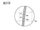
901、911‧‧‧初始特性901、911‧‧‧Initial characteristics
902、912‧‧‧-BT902, 912‧‧‧-BT
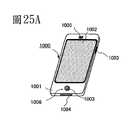
1000‧‧‧行動電話1000‧‧‧Mobile
1001、2701、2703、9401、9411、9601、9701、9881、9891、9901、2701、2703、9401、9411、9601、9701、9881、9891、9901‧‧‧外殼1001, 2701, 2703, 9401, 9411, 9601, 9701, 9881, 9891, 9901, 2701, 2703, 9401, 9411, 9601, 9701, 9881, 9891, 9901 ‧‧‧
1002、2705、2707、9412、9603、9607、9703、9882、9883、9903‧‧‧顯示部1002, 2705, 2707, 9412, 9603, 9607, 9703, 9882, 9883, 9903 ‧‧‧ Display
1003、9402、9413‧‧‧操作按鈕1003, 9402, 9413 ‧‧‧ operation buttons
1004‧‧‧外部連接埠1004‧‧‧External port
1005、2725、9405‧‧‧揚聲器1005, 2725, 9405 ‧‧‧ speaker
1006、9404、9889‧‧‧麥克風1006, 9404, 9889‧‧‧ microphone
105a‧‧‧源極電極層105a‧‧‧Source electrode layer
105b‧‧‧汲極電極層105b‧‧‧Drain electrode layer
2601‧‧‧相對基板2601‧‧‧Relative substrate
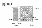
2602、4005、4505‧‧‧密封劑2602、4005、4505‧‧‧‧sealant
2603、4002、4502、5301‧‧‧畫素部2603, 4002, 4502, 5301 ‧‧‧ pixel unit
2604‧‧‧顯示元件2604‧‧‧Display element
2605‧‧‧著色層2605‧‧‧Coloring layer
2606、2607‧‧‧偏光板2606, 2607‧‧‧ Polarizer
2608‧‧‧布線電路部2608‧‧‧Wiring Circuit Department
2609‧‧‧軟性布線板2609‧‧‧flexible wiring board
2610‧‧‧冷陰極管2610‧‧‧Cold cathode tube
2611‧‧‧反射板2611‧‧‧Reflective plate
2612‧‧‧電路板2612‧‧‧ circuit board
2613‧‧‧擴散板2613‧‧‧Diffusion plate
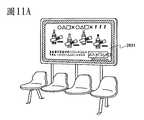
2631‧‧‧海報2631‧‧‧Poster
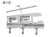
2632‧‧‧車廂廣告2632‧‧‧Car advertisement
2700‧‧‧電子書閱讀器2700‧‧‧ e-book reader
2711‧‧‧絞鏈2711‧‧‧ hinge
2721‧‧‧電源開關2721‧‧‧Power switch
2723、9609、9885‧‧‧操作鍵2723、9609、9885‧‧‧operation keys
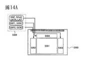
4003、4503a、4503b、5304‧‧‧信號線驅動電路4003, 4503a, 4503b, 5304 ‧‧‧ signal line driver circuit
4004、4504a、4504b、5302、5303‧‧‧掃描線驅動電路4004, 4504a, 4504b, 5302, 5303 ‧‧‧ scanning line drive circuit
4008‧‧‧液晶層4008‧‧‧Liquid crystal layer
4013‧‧‧液晶元件4013‧‧‧Liquid crystal element
4015、4515‧‧‧連接終端電極4015、4515‧‧‧Connect terminal electrode
4016、4516‧‧‧終端電極4016, 4516‧‧‧ terminal electrode
4018、4518a、4518b‧‧‧軟性印刷電路(FPC)4018, 4518a, 4518b ‧‧‧ flexible printed circuit (FPC)
4019、4519‧‧‧各向異性導電膜4019, 4519 ‧‧‧ anisotropic conductive film
4031‧‧‧相對電極層4031‧‧‧Counter electrode layer
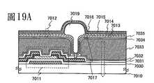
4511、6404、7002、7012、7022‧‧‧發光元件4511, 6404, 7002, 7012, 7022
4512‧‧‧電致發光層4512‧‧‧Electroluminescence layer
4520、7009、7019、7029‧‧‧分割區4520, 7009, 7019, 7029 ‧‧‧ division
5305‧‧‧時序控制電路5305‧‧‧sequence control circuit
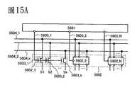
5601‧‧‧移位暫存器5601‧‧‧Shift register
5602‧‧‧開關電路5602‧‧‧Switch circuit
590k‧‧‧黑區590k‧‧‧Black Zone
590b‧‧‧白區590b‧‧‧White District
6400‧‧‧畫素6400‧‧‧ pixels
6401‧‧‧開關電晶體6401‧‧‧Switch transistor
6402‧‧‧驅動電晶體6402‧‧‧Drive transistor
6403‧‧‧電容器6403‧‧‧Capacitor
6405‧‧‧信號線6405‧‧‧Signal cable
6406‧‧‧掃描線6406‧‧‧scan line
6408‧‧‧共同電極6408‧‧‧Common electrode
7004、7014、7024、‧‧‧電致發光(EL)層7004, 7014, 7024, ‧‧‧ electroluminescence (EL) layer
7016‧‧‧阻光膜7016‧‧‧Light blocking film
7033、7043‧‧‧濾色器層7033, 7043‧‧‧ color filter layer
7034、7044‧‧‧覆膜層7034、7044‧‧‧Coated layer
7035、7045、7052‧‧‧保護絕緣層7035, 7045, 7052‧‧‧protective insulating layer
7053‧‧‧平面化絕緣層7053‧‧‧planar insulating layer
9400‧‧‧通訊裝置9400‧‧‧Communication device
9403‧‧‧外部輸入端子9403‧‧‧External input terminal
9406‧‧‧發光部9406‧‧‧Lighting Department
9410‧‧‧顯示裝置9410‧‧‧Display device
9600‧‧‧電視裝置9600‧‧‧TV installation
9605‧‧‧支架9605‧‧‧Bracket
9610‧‧‧遙控器9610‧‧‧Remote control
9700‧‧‧數位相框9700‧‧‧Digital Photo Frame
9884‧‧‧揚聲器部9884‧‧‧Speaker Department
9886‧‧‧記錄媒體嵌入部9886‧‧‧Recording Media Embedding Department
9887‧‧‧連接端子9887‧‧‧Connecting terminal
9888‧‧‧感應器9888‧‧‧sensor
9890‧‧‧發光二極體(LED)燈9890‧‧‧Light emitting diode (LED) lamp
9893‧‧‧接合部9893‧‧‧Joint
9900‧‧‧投幣機9900‧‧‧Slot machine
圖1A及1B為截面圖,各描繪電晶體。1A and 1B are cross-sectional views, each depicting a transistor.
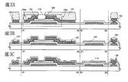
圖2A至2C為電晶體之截面程序圖。2A to 2C are cross-sectional process diagrams of transistors.
圖3A至3C為電晶體之截面程序圖。3A to 3C are cross-sectional program diagrams of transistors.
圖4A及4B為平面圖,描繪電晶體。4A and 4B are plan views depicting transistors.
圖5為平面圖,描繪電晶體。Figure 5 is a plan view depicting a transistor.
圖6為平面圖,描繪電晶體。Figure 6 is a plan view depicting a transistor.
圖7為平面圖,描繪電晶體。7 is a plan view depicting transistors.
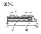
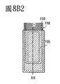
圖8A1、8A2、8B1及8B2為平面圖及截面圖,描繪閘極布線端子部。8A1, 8A2, 8B1, and 8B2 are plan views and cross-sectional views illustrating gate wiring terminal portions.
圖9為平面圖,描繪電晶體。Figure 9 is a plan view depicting a transistor.
圖10A及10B為平面圖,各描繪電晶體。10A and 10B are plan views, each depicting a transistor.
圖11A及11B各描繪顯示裝置之應用範例。11A and 11B each depict an application example of a display device.
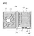
圖12為外部圖,描繪顯示裝置之範例。FIG. 12 is an external view depicting an example of a display device.
圖13為截面圖,描繪顯示裝置。13 is a cross-sectional view depicting a display device.
圖14A及14B為方塊圖,描繪液晶顯示裝置。14A and 14B are block diagrams depicting a liquid crystal display device.
圖15A及15B分別為信號線驅動電路之組態圖及時序圖。15A and 15B are a configuration diagram and a timing diagram of a signal line driving circuit, respectively.
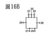
圖16A至16D為電路圖,各描繪移位暫存器之組態。16A to 16D are circuit diagrams each depicting the configuration of the shift register.
圖17A及17B分別為描繪移位暫存器之組態的電路圖,及描繪移位暫存器之作業的時序圖。17A and 17B are a circuit diagram depicting the configuration of the shift register, and a timing diagram depicting the operation of the shift register, respectively.
圖18描繪顯示裝置之畫素等效電路。FIG. 18 depicts the pixel equivalent circuit of the display device.
圖19A至19C為截面圖,各描繪顯示裝置。19A to 19C are cross-sectional views, each depicting a display device.
圖20A1、20A2、20B為平面圖及截面圖,描繪顯示裝置。20A1, 20A2, and 20B are plan and cross-sectional views depicting a display device.
圖21為截面圖,描繪顯示裝置。21 is a cross-sectional view depicting the display device.
圖22A及22B為平面圖及截面圖,分別描繪顯示裝置。22A and 22B are plan and cross-sectional views respectively depicting the display device.
圖23A及23B為外部圖,分別描繪電視裝置及數位相框之範例。23A and 23B are external diagrams depicting examples of television devices and digital photo frames, respectively.
圖24A及24B為外部圖,描繪遊戲機之範例。24A and 24B are external diagrams depicting examples of gaming machines.
圖25A及25B為外部圖,描繪行動電話之範例。25A and 25B are external diagrams depicting examples of mobile phones.
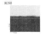
圖26A及26B為氧化物半導體層之截面的TEM照片。26A and 26B are TEM photographs of the cross section of the oxide semiconductor layer.
圖27A及27B為氧化物半導體層之截面的TEM照片。27A and 27B are TEM photographs of the cross section of the oxide semiconductor layer.
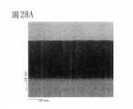
圖28A及28B為氧化物半導體層之截面的TEM照片。28A and 28B are TEM photographs of the cross section of the oxide semiconductor layer.
圖29A及29B分別為氧化物半導體層之截面的TEM照片及電子衍射圖。29A and 29B are TEM of the cross section of the oxide semiconductor layerPhotos and electron diffraction patterns.
圖30為氧化物半導體層之EDX頻譜分析。Fig. 30 is an EDX spectrum analysis of the oxide semiconductor layer.
圖31為氧化物半導體層之X光衍射圖。Fig. 31 is an X-ray diffraction chart of an oxide semiconductor layer.
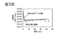
圖32A至32C為氧化物半導體層之SIMS深度分析數據圖。32A to 32C are SIMS depth analysis data charts of oxide semiconductor layers.
圖33簡要描繪科學計算。Figure 33 briefly depicts scientific computing.
圖34A及34B簡要描繪科學計算。Figures 34A and 34B briefly depict scientific computing.
圖35A及35B描繪科學計算。Figures 35A and 35B depict scientific computing.
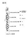
圖36描繪氧化物半導體之晶體結構。Fig. 36 depicts the crystal structure of an oxide semiconductor.
圖37A及37B顯示未歷經-BT測試及已歷經-BT測試之電晶體的I-V特性。37A and 37B show the I-V characteristics of transistors that have not undergone -BT testing and have undergone -BT testing.
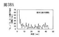
圖38A至38C為氧化物半導體層之SIMS深度分析數據圖。38A to 38C are SIMS in-depth analysis data charts of oxide semiconductor layers.
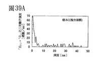
圖39A至39C為氧化物半導體層之SIMS深度分析數據圖。39A to 39C are SIMS in-depth analysis data charts of oxide semiconductor layers.
將參考圖式描述實施例及範例。請注意,本發明不侷限於下列描述,本技藝中技術熟練人士將輕易理解在不偏離本發明之精神及範圍下,本發明之模式及細節可以各種方式修改。因此,本發明不應解釋為侷限於下列實施例及範例之描述。請注意,在下列所描述本發明之結構中,不同圖式中具有類似功能之相同部分將標示相同編號,並省略其描述。The embodiments and examples will be described with reference to the drawings. Please note that the present invention is not limited to the following description. Those skilled in the art will easily understand that the modes and details of the present invention can be modified in various ways without departing from the spirit and scope of the present invention. Therefore, the present invention should not be interpreted as being limited to the description of the following embodiments and examples. Please note that in the structure of the present invention described below, the same parts with similar functions in different drawings will be marked with the same numbers and their descriptions will be omitted.
在本實施例中,將參照圖1A及1B描述電晶體之結構。In this embodiment, the structure of the transistor will be described with reference to FIGS. 1A and 1B.
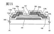
圖1A為通道蝕刻電晶體之截面圖,而圖4A為其平面圖。圖1A為沿圖4A之線A1-A2之截面圖。FIG. 1A is a cross-sectional view of a channel-etched transistor, and FIG. 4A is a plan view thereof. FIG. 1A is a cross-sectional view taken along line A1-A2 of FIG. 4A.
圖1A及1B中所描繪之電晶體,各包括於基板100上之閘極電極層101、閘極絕緣層102、包括表面部分之結晶區106的氧化物半導體層103、源極電極層105a及汲極電極層105b。氧化物絕緣層107係置於包括表面部分之結晶區106的氧化物半導體層103、源極電極層105a及汲極電極層105b之上。The transistors depicted in FIGS. 1A and 1B each include a
請注意,圖1A描繪正常通道蝕刻電晶體之結構,其中部分氧化物半導體層於源極電極層105a及汲極電極層105b之間蝕刻;然而,可替代地使用一種結構,如圖1B中所描繪,其中氧化物半導體層未蝕刻,使得表面部分之結晶區留下。Please note that FIG. 1A depicts the structure of a normal channel etch transistor, in which part of the oxide semiconductor layer is etched between the
閘極電極層101可由使用任何金屬材料之單層結構或層級結構組成,諸如鋁、銅、鉬、鈦、鉻、鉭、鎢、釹及鈧;包含該些金屬材料之任一項做為其主要成分之合金材料;或包含該些金屬材料之任一項之氮化物。若諸如鋁或銅之低電阻金屬材料被用做電極層,因其具有諸如低耐熱及易於腐蝕之缺點,該低電阻金屬材料較佳地與耐火金屬材料組合使用。有關耐火金屬材料,可使用鉬、鈦、鉻、鉭、鎢、釹、鈧等。The
此外,為提升畫素部之孔徑比,銦氧化物之透光氧化物導電層、銦氧化物及錫氧化物合金、銦氧化物及鋅氧化物合金、鋅氧化物、鋅鋁氧化物、鋅鋁氮氧化合物、鋅鎵氧化物等可用做閘極電極層101。In addition, in order to improve the aperture ratio of the pixel portion, the transparent oxide conductive layer of indium oxide, indium oxide and tin oxide alloy, indium oxide and zinc oxide alloy, zinc oxide, zinc aluminum oxide, zinc Aluminum oxynitride, zinc gallium oxide, etc. can be used as the
有關閘極絕緣層102,可使用矽氧化物、矽氮氧化合物、矽氮化物氧化物、矽氮化物、鋁氧化物、鉭氧化物等任一項之單層膜或複合膜。該等膜可以CVD法、噴濺法等予以形成。For the
有關氧化物半導體膜,可使用以InMO3(ZnO)m(m>0)表示之薄膜。此處,M代表一或多項選自Ga、Al、Mn及Co之金屬元件。例如,M可為Ga、Ga及Al、Ga及Mn、Ga及Co等。在以InMO3(ZnO)m(m>0)表示之氧化物半導體膜中,包括Ga做為M之氧化物半導體稱為In-Ga-Zn-O基氧化物半導體,及In-Ga-Zn-O基氧化物半導體之薄膜亦稱為In-Ga-Zn-O基膜。For the oxide semiconductor film, a thin film expressed by InMO3 (ZnO)m (m>0) can be used. Here, M represents one or more metal elements selected from Ga, Al, Mn, and Co. For example, M may be Ga, Ga and Al, Ga and Mn, Ga and Co, or the like. In the oxide semiconductor film represented by InMO3 (ZnO)m (m>0), an oxide semiconductor including Ga as M is called an In-Ga-Zn-O-based oxide semiconductor, and In-Ga-Zn The thin film of -O-based oxide semiconductor is also called In-Ga-Zn-O-based film.
氧化物半導體層103係以噴濺法形成具有10nm至300nm厚度,較佳地為20nm至100nm。應注意的是,如圖1A中所描繪,若部分氧化物半導體層103被蝕刻,當裝置完成時,氧化物半導體層103便具有一區域其厚度小於上述厚度。The
有關氧化物半導體層103,係使用以RTA法等於高溫下短時間執行脫水或脫氫者。脫水或脫氫可以高溫氣體(諸如氮或稀有氣體之惰性氣體)經由快速熱退火(RTA)處理,或以500℃至750℃(或低於或等於玻璃基板之應變點的溫度)之光執行約一分鐘至十分鐘,較佳地以650℃執行約三分鐘至六分鐘。基於RTA法,可以短時間執行脫水或脫氫;因此,可以高於玻璃基板之應變點的溫度執行處理。Regarding the
氧化物半導體層103為於氧化物半導體層103形成階段具有許多懸鍵之非結晶層。經過脫水或脫氫之加熱步驟,短距離內懸鍵彼此黏合,使得氧化物半導體層103可具有有序的非結晶結構。隨著定序進行,氧化物半導體層103成為由非結晶及微晶之混合物組成,此處非結晶區滿布微晶,或由微晶群組成。此處,微晶為具1nm至20nm粒子尺寸之所謂奈米晶體,其小於一般稱為微晶的微晶粒子。The
微晶層較佳地在氧化物半導體層103的表面中形成,該表面部分為結晶區106,微晶在微晶層中為垂直於該層表面方向之c軸取向。在此狀況下,晶體之長軸呈c軸方向,而短軸方向之晶體為1nm至20nm。The microcrystalline layer is preferably formed in the surface of the
在氧化物半導體層的表面部分,其具有一結構,存在包括微晶之密集結晶區,因而可以避免由於轉變為n型,歸因於濕氣進入表面部分或排除表面部分之氧,而造成之電氣特性降低。此外,由於氧化物半導體層的表面部分在背通道側,可避免氧化物半導體層轉變為n型,亦可有效抑制寄生通道的產生。而且,可減少由於結晶區及源極電極層105a或汲極電極層105b存在而電導度增加之表面部分之間的接觸電阻。On the surface part of the oxide semiconductor layer, it has a structure with dense crystalline regions including crystallites, so that it can be avoided due to the conversion to n-type due to moisture entering the surface part or excluding oxygen from the surface part The electrical characteristics are reduced. In addition, since the surface portion of the oxide semiconductor layer is on the back channel side, the oxide semiconductor layer can be prevented from changing to an n-type, and the generation of parasitic channels can also be effectively suppressed. Moreover, the surface portion where the electrical conductivity is increased due to the presence of the crystal region and the
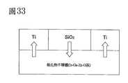
此處,極可能生長之In-Ga-Zn-O基膜的晶體結構,取決於沈積氧化物半導體所用之目標。例如,若使用用以沈積氧化物半導體之目標而形成In-Ga-Zn-O基膜,其包含In、Ga及Zn,使得In2O3相對於Ga2O3相對於ZnO之摩爾比為1:1:1,並經由加熱步驟執行晶化,而可能形成六角晶系層狀化合物晶體結構,其中包含Ga及Zn的一氧化物層或二氧化物層混合於In氧化物層之間。另一方面,若使用In2O3相對於Ga2O3相對於ZnO之摩爾比為1:1:2之目標,並經由加熱步驟執行晶化,包含Ga及Zn並插入In氧化物層之間的氧化物層可能具有雙層結構。由於包含Ga及Zn並具有雙層結構之氧化物層的晶體結構是穩定的,因而可能發生晶體生長,若使用In2O3相對於Ga2O3相對於ZnO之摩爾比為1:1:2之目標,並經由加熱步驟執行晶化,有時形成從包含Ga及Zn之氧化物層的外層至閘極絕緣膜與包含Ga及Zn之氧化物層之間接合部的連續晶體。請注意,摩爾比可稱為原子比。Here, the crystal structure of the In-Ga-Zn-O-based film that is likely to grow depends on the target used to deposit the oxide semiconductor. For example, if a target for depositing an oxide semiconductor is used to form an In-Ga-Zn-O-based film, which includes In, Ga, and Zn, such that the molar ratio of In2 O3 to Ga2 O3 to ZnO is 1:1:1, and performing crystallization through a heating step, it is possible to form a hexagonal layered compound crystal structure in which an oxide layer or a dioxide layer containing Ga and Zn is mixed between the In oxide layers. On the other hand, if the target of using a molar ratio of In2 O3 to Ga2 O3 to ZnO of 1:1:2 and performing crystallization through a heating step, including Ga and Zn and inserting the In oxide layer The interlayer oxide layer may have a double-layer structure. Since the crystal structure of the oxide layer including Ga and Zn and having a double-layer structure is stable, crystal growth may occur. If the molar ratio of In2 O3 to Ga2 O3 to ZnO is 1:1: The objective of 2, and performing crystallization through a heating step, sometimes forms a continuous crystal from the outer layer of the oxide layer containing Ga and Zn to the junction between the gate insulating film and the oxide layer containing Ga and Zn. Please note that the molar ratio can be called atomic ratio.
請注意,如圖10A中所描繪,結晶區並未形成於氧化物半導體層103的側表面部,取決於步驟順序,且結晶區106僅形成於上層部。應注意的是側表面部的面積率低,因而在此狀況下亦可保持上述效果。Please note that as depicted in FIG. 10A, the crystalline region is not formed on the side surface portion of the
源極電極層105a具有第一導電層112a、第二導電層113a及第三導電層114a之三層結構,同時汲極電極層105b具有第一導電層112b、第二導電層113b及第三導電層114b之三層結構。有關源極及汲極電極層105a及105b之材料,可使用類似於閘極電極層101之材料。The
此外,透光氧化物導電層係以類似於閘極電極層101之方式用於源極及汲極電極層105a及105b,藉此可提升畫素部之透光性,亦可提升孔徑比。In addition, the light-transmitting oxide conductive layer is used for the source and drain
此外,氧化物導電層可形成於氧化物半導體層103與上述金屬膜之間,做為源極及汲極電極層105a及105b,使得可減少接觸電阻。In addition, an oxide conductive layer can be formed between the
做為通道保護層之氧化物絕緣層107係設於氧化物半導體層103、源極電極層105a及汲極電極層105b之上。氧化物絕緣層係使用無機絕緣膜以噴濺法形成,典型為矽氧化物膜、矽氮化物氧化物膜、鋁氧化物膜、鋁氮氧化合物膜等。An
另一方面,圖10B中所描繪之底部接觸型電晶體可使用類似於各部之材料形成。On the other hand, the bottom-contact transistor depicted in FIG. 10B may be formed using materials similar to the parts.
圖10B中所描繪之電晶體包括基板100上之閘極電極層101、閘極絕緣層102、源極電極層105a、汲極電極層105b、及包括表面部分之晶體區106之氧化物半導體層103。此外,氧化物絕緣層107係設於閘極絕緣層102、源極電極層105a、汲極電極層105b及氧化物半導體層103之上。The transistor depicted in FIG. 10B includes the
亦在此結構中,氧化物半導體層103為非結晶或由非結晶及微晶之混合物組成,除了表面部分包括微晶層組成之結晶區106外,此處非結晶區滿布微晶或由微晶群組成。當使用具有該等結構之氧化物半導體層時,可以類似於通道蝕刻結構之方式,避免由於轉變為n型,歸因於濕氣進入表面部分或排除表面部分之氧,而造成之電氣特性降低。此外,由於氧化物半導體層之表面部分在背通道側,並包括微晶層組成之結晶區,可抑制寄生通道之產生。Also in this structure, the
基於該等結構,電晶體可具有高可靠性及高電氣特性。Based on these structures, the transistor can have high reliability and high electrical characteristics.
請注意,儘管在本實施例中提供通道蝕刻電晶體之範例,但可使用通道保護電晶體。另一方面,可使用包括與源極電極層及汲極電極層重疊之氧化物半導體層的底部接觸型電晶體。Please note that although an example of channel etching transistors is provided in this embodiment, channel protection transistors may be used. On the other hand, a bottom contact type transistor including an oxide semiconductor layer overlapping with the source electrode layer and the drain electrode layer can be used.
請注意,本實施例中所描述之結構可用於酌情與其他實施例中所描述之任何結構相組合。Please note that the structure described in this embodiment can be used in combination with any structure described in other embodiments as appropriate.
在本實施例中,將參照圖2A至2C、圖3A至3C、圖4A及4B、圖5、圖6、圖7、圖8A1、8A2、8B1和8B2及圖9描述實施例1中所描述之包括通道蝕刻電晶體之顯示裝置的製造程序。圖2A至2C及圖3A至3C為截面圖,圖4A及4B、圖5、圖6及圖7為平面圖,及圖4A及4B中線A1-A2及線B1-B2、圖5、圖6及圖7分別相應於圖2A至2C及圖3A至3C之截面圖中線A1-A2及線B1-B2。In this embodiment, the description in
首先,準備基板100。有關基板100,可使用任一下列基板;以熔融法或浮標法由鋇硼矽酸鹽玻璃、鋁硼矽酸鹽玻璃、鋁矽酸鹽玻璃等製成之非鹼性玻璃基板、陶瓷基板、具有足以支撐本製造程序之處理溫度之耐熱的塑料基板等。另一方面,可使用金屬基板,諸如表面具絕緣膜之不銹鋼合金基板。First, the
請注意,除了上述玻璃基板外,可使用絕緣體形成之基板做為基板100,諸如陶瓷基板、石英基板或藍寶石基板。Please note that in addition to the above-mentioned glass substrate, a substrate formed of an insulator can be used as the
此外,有關基膜,絕緣膜可形成於基板100之上。基膜可以CVD法、噴濺法等,使用矽氧化物膜、矽氮化物膜、矽氮氧化合物膜及矽氮化物氧化物膜之任一項形成具單層結構或層級結構。若使用包含移動離子之基板做為基板100,諸如玻璃基板,便使用包含氮之膜做為基膜,諸如矽氮化物膜或矽氮化物氧化物膜,藉此可避免移動離子進入半導體層。In addition, regarding the base film, an insulating film may be formed on the
其次,成為包括閘極電極層101、電容器布線108及第一端子121之閘極布線的導電膜,係以以噴濺法或真空蒸發法形成於基板100的整個表面上。其次,經由第一光刻程序形成抗蝕罩。藉由蝕刻移除不必要部分,以形成布線及電極(包括電極層101之閘極布線、電容器布線108及第一端子121)。此時,較佳地執行蝕刻,使得閘極電極層101之端部呈錐形,以避免形成於閘極電極層101上之膜破裂。圖2A中描繪本階段之截面圖。請注意,圖4B為本階段之平面圖。Next, a conductive film that becomes the gate wiring including the
包括閘極電極層101、電容器布線108及端子部中第一端子121之閘極布線,可由使用任何金屬材料之單層結構或層級結構組成,諸如鋁、銅、鉬、鈦、鉻、鉭、鎢、釹及鈧;包含任一項該些金屬材料做為其主要成分之合金材料;或包含任一項該些金屬材料之氮化物。若諸如鋁或銅之低電阻金屬材料被用做電極層,因其具有諸如低耐熱及易於腐蝕之缺點,該低電阻金屬材料較佳地與耐火金屬材料組合使用。有關耐火金屬材料,可使用鉬、鈦、鉻、鉭、鎢、釹、鈧等。The gate wiring including the
例如,有關閘極電極層101之雙層結構,下列結構較佳:其中鉬層堆疊於鋁層之上之雙層結構、其中鉬層堆疊於銅層之上之雙層結構、其中鈦氮化物層或鉭氮化物層堆疊於銅層之上之雙層結構、及鈦氮化物層及鉬層之雙層結構。有關三層結構,下列結構較佳:包括鋁之層級結構、鋁及矽之合金、鋁及鈦之合金、或鋁及中間層之釹及頂部層及底部層之鎢、鎢氮化物、鈦氮化物及鈦之任一項之合金。For example, regarding the double-layer structure of the
當時,透光氧化物導電層係用於部分電極層及布線層,以增加孔徑比。例如,銦氧化物、銦氧化物及錫氧化物之合金、銦氧化物及鋅氧化物之合金、鋅氧化物、鋅鋁氧化物、鋅鋁氮氧化合物、鋅鎵氧化物等合金,可用於氧化物導電層。At that time, the transparent oxide conductive layer was used for part of the electrode layer and the wiring layer to increase the aperture ratio. For example, indium oxide, indium oxide and tin oxide alloys, indium oxide and zinc oxide alloys, zinc oxide, zinc aluminum oxide, zinc aluminum oxynitride, zinc gallium oxide and other alloys can be used Oxide conductive layer.
其次,閘極絕緣層102形成於閘極電極層101之上。閘極絕緣層102以CVD法、噴濺法等形成50nm至250nm之厚度。Next, the
例如,對閘極絕緣層102而言,以噴濺法形成具100nm厚度之矽氧化物膜。不用說,閘極絕緣層102不侷限於該等矽氧化物膜,並可形成而具使用任一項絕緣膜之單層結構或層級結構,諸如矽氮氧化合物膜、矽氮化物氧化物膜、矽氮化物膜、鋁氧化物膜及鉭氧化物膜。For example, for the
另一方面,閘極絕緣層102可以CVD法經有機矽烷氣體而使用矽氧化物層予以形成。對有機矽烷氣體而言,可使用包含矽之化合物,諸如四乙氧基矽烷(TEOS)、四甲基矽烷(TMS)、四甲基環四矽氧烷(TMCTS)、八甲基環四矽氧烷(OMCTS)、六甲基二矽氮烷(HMDS)、三乙氧基矽烷(TRIES)或三(二甲氨基)矽烷(TDMAS)。On the other hand, the
另一方面,閘極絕緣層102可使用鋁、釔或鉿之氧化物、氮化物、氮氧化合物及氮化物氧化物,或包括上述之至少二或更多類之化合物予以形成。On the other hand, the
請注意,在本說明書中,「氮氧化合物」乙詞係指一種包含氧原子及氮原子之物質,使得氧原子之數量大於氮原子之數量,而「氮化物氧化物」乙詞係指一種包含氮原子及氧原子之物質,使得氮原子之數量大於氧原子之數量。例如,「矽氮氧化合物膜」意即包含氧原子及氮原子之膜,使得氧原子之數量大於氮原子之數量,若使用盧瑟福背散射光譜學(RBS)及氫前向散射(HFS)執行測量,所包含氧、氮、矽及氫之濃度範圍各為50原子%至70原子%、0.5原子%至15原子%、25原子%至35原子%及0.1原子%至10原子%。此外,「矽氮化物氧化物膜」意即包含氮原子及氧原子之膜,使得氮原子之數量大於氧原子之數量,若使用RBS及HFS執行測量,所包含氧、氮、矽及氫之濃度範圍各為5原子%至30原子%、20原子%至55原子%、25原子%至35原子%及10原子%至30原子%。請注意,氮、氧、矽及氫之百分比均落於上述範圍內,其中矽氮氧化合物膜或矽氮化物氧化物膜中所包含之總原子數定義為100原子%。Please note that in this specification, the term "nitrogen oxide" refers to a substance containing oxygen atoms and nitrogen atoms, so that the number of oxygen atoms is greater than the number of nitrogen atoms, and the term "nitride oxide" refers to a A substance containing nitrogen atoms and oxygen atoms makes the number of nitrogen atoms greater than the number of oxygen atoms. For example, "silicon oxynitride film" means a film containing oxygen atoms and nitrogen atoms, so that the number of oxygen atoms is greater than the number of nitrogen atoms, if you use LutherFortune backscattering spectroscopy (RBS) and hydrogen forward scattering (HFS) perform measurements. The concentration ranges of oxygen, nitrogen, silicon and hydrogen included are 50 atom% to 70 atom%, 0.5 atom% to 15 atom%, 25 Atom% to 35 atom% and 0.1 atom% to 10 atom%. In addition, "silicon nitride oxide film" means a film containing nitrogen atoms and oxygen atoms, so that the number of nitrogen atoms is greater than the number of oxygen atoms. If RBS and HFS are used to perform the measurement, the oxygen, nitrogen, silicon and hydrogen The concentration ranges are 5 to 30 atomic%, 20 to 55 atomic%, 25 to 35 atomic%, and 10 to 30 atomic%. Please note that the percentages of nitrogen, oxygen, silicon, and hydrogen all fall within the above range, where the total number of atoms contained in the silicon oxynitride film or silicon nitride oxide film is defined as 100 atom%.
請注意,在用於形成氧化物半導體層103之氧化物半導體膜形成之前,閘極絕緣層表面上之灰塵較佳地經由執行反向噴濺而予移除,其中導入氬氣並產生電漿。反向噴濺係指一種方法,其中RF電源用於將電壓應用於氬氣中之基板側,使得於基板周圍產生電漿以修改表面。請注意,除了氬氣外,可使用氮氣、氦氣等。另一方面,可使用添加氧、N2O等之氬氣。再另一方面,可使用添加Cl2、CF4等之氬氣。在反向噴濺之後,形成氧化物半導體膜而不暴露於空氣,藉此可避免灰塵及濕氣附著至閘極絕緣層102及氧化物半導體層103之間之接合部。Please note that before the oxide semiconductor film used to form the
其次,氧化物半導體膜形成於閘極絕緣層102之上,達5nm至200nm厚度,較佳地為10nm至40nm。Secondly, an oxide semiconductor film is formed on the
有關氧化物半導體膜,可使用諸如In-Sn-Ga-Zn-O基膜之四元金屬氧化物膜;諸如In-Ga-Zn-O基膜、In-Sn-Zn-O基膜、In-Al-Zn-O基膜、Sn-Ga-Zn-O基膜、Al-Ga-Zn-O基膜或Sn-Al-Zn-O基膜之三元金屬氧化物膜;或諸如In-Zn-O基膜、Sn-Zn-O基膜、Al-Zn-O基膜、Zn-Mg-O基膜、Sn-Mg-O基膜、或In-Mg-O基膜之二元金屬氧化物膜;In-O基膜、Sn-O基膜或Zn-O基膜。此外,氧化物半導體膜可進一步包含SiO2。For the oxide semiconductor film, a quaternary metal oxide film such as In-Sn-Ga-Zn-O-based film; such as In-Ga-Zn-O-based film, In-Sn-Zn-O-based film, In -Al-Zn-O-based film, Sn-Ga-Zn-O-based film, Al-Ga-Zn-O-based film, or ternary metal oxide film of Sn-Al-Zn-O-based film; or such as In- Binary metals of Zn-O-based film, Sn-Zn-O-based film, Al-Zn-O-based film, Zn-Mg-O-based film, Sn-Mg-O-based film, or In-Mg-O-based film Oxide film; In-O-based film, Sn-O-based film or Zn-O-based film. In addition, the oxide semiconductor film may further contain SiO2 .
此處,使用用於氧化物半導體沈積之目標而形成氧化物半導體膜,其包含In、Ga及Zn(In2O3相對於Ga2O3相對於ZnO之比例為1:1:1或1:1:2摩爾比),在基板及目標之間距離為100mm、壓力為0.6Pa及直流(DC)電力為0.5kW等狀況下,且氣體為氧氣(氧流比例為100%)。請注意,當使用脈衝直流(DC)電源時,可減少灰塵且膜厚度可能為均勻。在本實施例中,有關氧化物半導體膜,以噴濺法並使用用於In-Ga-Zn-O基氧化物半導體沈積之目標形成30-nm厚之In-Ga-Zn-O基膜。Here, an oxide semiconductor film is formed using a target for oxide semiconductor deposition, which includes In, Ga, and Zn (the ratio of In2 O3 to Ga2 O3 to ZnO is 1:1:1 or 1 : 1:2 molar ratio), under the conditions that the distance between the substrate and the target is 100 mm, the pressure is 0.6 Pa, and the direct current (DC) power is 0.5 kW, and the gas is oxygen (the proportion of oxygen flow is 100%). Please note that when pulsed direct current (DC) power is used, dust can be reduced and the film thickness may be uniform. In this embodiment, regarding the oxide semiconductor film, a 30-nm-thick In-Ga-Zn-O-based film is formed by a sputtering method and using a target for In-Ga-Zn-O-based oxide semiconductor deposition.
噴濺法之範例包括RF噴濺法,其中高頻電源用做噴濺電源;DC噴濺法,其中使用DC電源;及脈衝DC噴濺法,其中以脈衝方式施予偏壓。RF噴濺法主要用於若形成絕緣膜;DC噴濺法主要用於若形成諸如金屬膜之導電膜。Examples of the sputtering method include an RF sputtering method in which a high-frequency power source is used as the sputtering power source; a DC sputtering method in which a DC power source is used; and a pulsed DC sputtering method in which a bias voltage is applied in a pulse manner. The RF sputtering method is mainly used for forming an insulating film; the DC sputtering method is mainly used for forming a conductive film such as a metal film.
此外,亦存在多重來源噴濺設備,其中可設定複數個不同材料之目標。基此多重來源噴濺設備,可形成不同材料之膜堆疊於相同腔室中,或可經由相同時間在相同腔室中形成複數類材料之膜。In addition, there are multiple sources of spray equipment, which can set a plurality of different material targets. Based on the multi-source sputtering equipment, films of different materials can be stacked in the same chamber, or can be in the same chamber through the same timeForm a film of plural materials.
此外,存在設於腔室內部具磁性系統並用於磁控管噴濺法之噴濺設備,及用於ECR噴濺法之噴濺設備,其中使用利用微波產生之電漿而未使用輝光放電。In addition, there are sputtering equipment provided with a magnetic system inside the chamber and used for the magnetron sputtering method, and sputtering equipment used for the ECR sputtering method, in which plasma generated using microwaves is used instead of glow discharge.
而且,有關使用噴濺法之沈積法,亦存在反應噴濺法,其中目標物質及噴濺氣體成分於沈積期間彼此化學反應,以形成其薄複合膜,及偏壓噴濺法,其中電壓亦於沈積期間應用於基板。Moreover, regarding the deposition method using the sputtering method, there is also a reactive sputtering method, in which the target substance and the sputtering gas component chemically react with each other during the deposition to form its thin composite film, and the bias sputtering method, in which the voltage is also Applied to the substrate during deposition.
其次,經由第二光刻程序,形成抗蝕罩。接著,蝕刻In-Ga-Zn-O基膜。在蝕刻中,諸如檸檬酸或草酸之有機酸可用做蝕刻劑。此處,經由利用ITO-07N(Kanto化學股份有限公司製造)之濕式蝕刻來蝕刻In-Ga-Zn-O基膜,以移除不必要部分。因而,In-Ga-Zn-O基膜經處理而具有島形,藉此形成氧化物半導體層103。氧化物半導體層103之端部經蝕刻而具有錐形,藉此可避免因梯級形狀造成布線破裂。請注意,此處蝕刻不侷限於濕式蝕刻,而是可執行乾式蝕刻。Next, through a second photolithography process, a resist mask is formed. Next, the In-Ga-Zn-O-based film is etched. In etching, organic acids such as citric acid or oxalic acid can be used as an etchant. Here, the In-Ga-Zn-O-based film is etched through wet etching using ITO-07N (manufactured by Kanto Chemical Co., Ltd.) to remove unnecessary parts. Thus, the In-Ga-Zn-O-based film is processed to have an island shape, thereby forming the
接著,氧化物半導體層歷經脫水或脫氫。用以脫水或脫氫之第一熱處理可使用高溫氣體(諸如氮之惰性氣體或稀有氣體)經由快速熱退火(RTA)處理而予執行,或500℃至750℃溫度(或低於或等於玻璃基板應變點之溫度)之光實施達約一分鐘至十分鐘,較佳地以650℃實施達約三分鐘至六分鐘。基於RTA法,可以短時間執行脫水或脫氫;因此,可以高於玻璃基板應變點之溫度執行處理。圖2B及圖5中分別描繪本階段之截面圖及本階段之平面圖。請注意,熱處理之時序不侷限於此時序,而是可執行複數倍,例如,光刻程序或沈積步驟之前或之後。Next, the oxide semiconductor layer undergoes dehydration or dehydrogenation. The first heat treatment for dehydration or dehydrogenation may be performed by rapid thermal annealing (RTA) treatment using a high temperature gas (such as an inert gas of nitrogen or a rare gas), or a temperature of 500°C to 750°C (or less than or equal to glass The temperature at the strain point of the substrate is applied for about one minute to ten minutes, preferably at 650°C for about three minutes to six minutes. Based on RTA method, dehydration or dehydrogenation can be performed in a short time; therefore, it can be performed at a temperature higher than the strain point of the glass substrateManagement. 2B and FIG. 5 respectively depict a cross-sectional view at this stage and a plan view at this stage. Please note that the timing of the heat treatment is not limited to this timing, but can be performed multiple times, for example, before or after the lithography process or the deposition step.
此處,氧化物半導體層103之表面部分經由第一熱處理而被晶化,因而成為具有包括微晶之結晶區106。氧化物半導體層103的其餘區域成為非結晶或由非結晶及微晶之混合物組成,此處非結晶區滿布微晶,或由微晶群組成。請注意,結晶區106為部分氧化物半導體層103,且以下「氧化物半導體層103」包括結晶區106。Here, the surface portion of the
請注意,在本說明書中,在諸如氮之惰性氣體或稀有氣體之氣體中之熱處理稱為用以脫水或脫氫之熱處理。在本說明書中,「脫氫」並非指以熱處理僅排除H2。為求方便,H、OH等之排除亦稱為「脫水或脫氫」。Please note that in this specification, heat treatment in an inert gas such as nitrogen or a rare gas is referred to as heat treatment for dehydration or dehydrogenation. In the present specification, "dehydrogenation" refers to the heat treatment is not only to exclude H2. For convenience, the exclusion of H, OH, etc. is also called "dehydration or dehydrogenation".
重要的是歷經脫水或脫氫之氧化物半導體層不應暴露於空氣,以避免水或氫進入氧化物半導體層。當使用經由將氧化物半導體層改變為低電阻氧化物半導體層所獲得之氧化物半導體層形成電晶體時,即,n型(例如n-型或n+型)氧化物半導體層經由執行脫水或脫氫,及經由將低電阻氧化物半導體層改變為高電阻氧化物半導體層,使得氧化物半導體層成為i型氧化物半導體層,電晶體之閾值電壓(Vth)為正,使得體現所謂正常關屬性。對用於顯示裝置之電晶體而言,較佳的是閘極電壓為儘可能接近0V之正閾值電壓。在主動式矩陣顯示裝置中,電路中所包括之電晶體的電氣特性是重要的,且顯示裝置之效能取決於電氣特性。尤其,電晶體之閾值電壓是重要的。若電晶體之閾值電壓為負,電晶體具有所謂正常開屬性,即當閘極電壓為0V時,電流流經源極電極及汲極電極之間,使得難以控制使用電晶體形成之電路。若電晶體之閾值電壓為正,但閾值電壓之絕對值為大,電晶體有時便無法執行切換作業,因為驅動電壓不夠高。若為n通道電晶體,較佳的是在正電壓應用做為閘極電壓之後,通道形成且汲極電流流動。通道未形成除非驅動電壓提升之電晶體,及當施予負電壓時通道形成且汲極電流流動之電晶體,均為不適用於電路之電晶體。It is important that the oxide semiconductor layer that has undergone dehydration or dehydrogenation should not be exposed to air to prevent water or hydrogen from entering the oxide semiconductor layer. When an oxide semiconductor layer obtained by changing an oxide semiconductor layer to a low-resistance oxide semiconductor layer is used to form a transistor, that is, an n-type (for example, n- type or n+ -type) oxide semiconductor layer is subjected to dehydration or Dehydrogenation, and by changing the low-resistance oxide semiconductor layer to a high-resistance oxide semiconductor layer, the oxide semiconductor layer becomes an i-type oxide semiconductor layer, and the threshold voltage (Vth ) of the transistor is positive, making the so-called normal Off attributes. For a transistor used in a display device, it is preferable that the gate voltage is a positive threshold voltage as close to 0V as possible. In an active matrix display device, the electrical characteristics of transistors included in the circuit are important, and the performance of the display device depends on the electrical characteristics. In particular, the threshold voltage of the transistor is important. If the threshold voltage of the transistor is negative, the transistor has the so-called normal on property, that is, when the gate voltage is 0V, current flows between the source electrode and the drain electrode, making it difficult to control the circuit formed using the transistor. If the threshold voltage of the transistor is positive, but the absolute value of the threshold voltage is large, the transistor sometimes cannot perform the switching operation because the driving voltage is not high enough. In the case of n-channel transistors, it is preferable that after a positive voltage is applied as the gate voltage, the channel is formed and the drain current flows. The channel does not form a transistor unless the driving voltage is increased, and a transistor formed when the channel is applied and a drain current flows when a negative voltage is applied, are not suitable for a circuit.
當從脫水或脫氫之溫度執行冷卻時,氣體必須從溫度上升或執行熱處理之氣體切換為不同氣體。例如,冷卻可在執行脫水或脫氫之熔爐中執行,同時熔爐填注高純度氧氣、高純度N2O氣或超乾燥空氣(具有-40℃或更低之露點,較佳地為-60℃或更低),而不暴露於空氣。When cooling is performed from the temperature of dehydration or dehydrogenation, the gas must be switched from a temperature rise or a gas that performs heat treatment to a different gas. For example, cooling can be performed in a furnace that performs dehydration or dehydrogenation, while the furnace is filled with high-purity oxygen, high-purity N2 O gas, or ultra-dry air (having a dew point of -40°C or lower, preferably -60 ℃ or lower) without exposure to air.
請注意,在第一熱處理中,較佳的是氣體中不包含水、氫等。另一方面,被導入熱處理設備之惰性氣體的純度較佳地為6N(99.9999%)或更高,更佳地為7N(99.99999%)或更高(即,雜質濃度為1ppm或更低,較佳地為0.1ppm或更低)。Please note that in the first heat treatment, it is preferable that the gas does not contain water, hydrogen, or the like. On the other hand, the purity of the inert gas introduced into the heat treatment equipment is preferably 6N (99.9999%) or higher, more preferably 7N (99.99999%) or higher (that is, the impurity concentration is 1 ppm or lower, which is It is preferably 0.1 ppm or less).
若在惰性氣體中執行熱處理,氧化物半導體層便改變為缺氧氧化物半導體層,使得氧化物半導體層經由熱處理而成為低電阻氧化物半導體層(即,n型(例如n-或n+型)氧化物半導體層)。之後,經由形成接觸氧化物半導體層之氧化物絕緣層,氧化物半導體層便被製成超氧狀態。因而,氧化物半導體層被製成i型;即,氧化物半導體層改變為高電阻氧化物半導體層。因此,可形成具有有利的電氣特性之高度可靠電晶體。If heat treatment is performed in an inert gas, the oxide semiconductor layer is changed to an oxygen-deficient oxide semiconductor layer, so that the oxide semiconductor layer becomes a low-resistance oxide semiconductor layer (ie, n-type (eg, n− or n+ type ) Oxide semiconductor layer). After that, by forming an oxide insulating layer in contact with the oxide semiconductor layer, the oxide semiconductor layer is made into a superoxide state. Thus, the oxide semiconductor layer is made i-type; that is, the oxide semiconductor layer is changed to a high-resistance oxide semiconductor layer. Therefore, highly reliable transistors having favorable electrical characteristics can be formed.
依據第一熱處理之狀況或氧化物半導體層之材料,氧化物半導體層可部分晶化。在第一熱處理之後,獲得缺氧及具有低電阻之氧化物半導體層103。在第一熱處理之後,載子濃度高於剛在膜形成之後之氧化物半導體膜的載子濃度,使得氧化物半導體層較佳地具有1 x 10¹⁸/cm3或更高之載子濃度。Depending on the condition of the first heat treatment or the material of the oxide semiconductor layer, the oxide semiconductor layer may be partially crystallized. After the first heat treatment, an
氧化物半導體層可於氧化物半導體膜處理成為島形氧化物半導體層之前執行第一熱處理。在此狀況下,於第一熱處理之後執行第二光刻程序。結晶區未形成於島形氧化物半導體層103之側表面部,結晶區106僅形成於氧化物半導體層103之上層部(參照圖10A)。The oxide semiconductor layer may perform a first heat treatment before the oxide semiconductor film is processed into an island-shaped oxide semiconductor layer. In this case, the second photolithography process is performed after the first heat treatment. The crystal region is not formed on the side surface portion of the island-shaped
其次,經由第三光刻程序,形成抗蝕罩。經由蝕刻移除不必要部分。以形成接觸孔,抵達由與閘極電極層101相同材料形成之布線或電極層。本接觸孔係提供而連接上述布線等與之後將形成之導電膜之間。Next, through a third photolithography process, a resist mask is formed. Unnecessary parts are removed via etching. In order to form a contact hole, the wiring or electrode layer formed of the same material as the
其次,以噴濺法或真空蒸發法於氧化物半導體層103及閘極絕緣層102之上形成第一導電層112、第二導電層113及第三導電層114,做為導電層。圖2C為本階段之截面圖。Next, a first
第一導電層112、第二導電層113及第三導電層114各使用類似於閘極電極層101之材料予以形成。The first
此處,第一導電層112及第三導電層114係使用耐熱導電材料之鈦予以形成,第二導電層113係使用包含釹之鋁合金予以形成。該等結構可利用鋁的低電阻屬性,並減少凸起產生。請注意,儘管在本實施例中導電層具有三層結構,但本發明之實施例不侷限於此。可使用單層結構或包括二層、四層或更多層之層級結構。例如,可使用鈦膜之單層結構,或鈦膜及包含矽之鋁膜的層級結構。Here, the first
其次,經由第四光刻程序,形成抗蝕罩131。經由蝕刻移除不必要部分,藉此形成源極及汲極電極層105a及105b、氧化物半導體層103及連接電極120。此時,濕式蝕刻或乾式蝕刻可用做蝕刻法。例如,當使用鈦而形成第一導電層112及第三導電層114時,及使用包含釹之鋁合金而形成第二導電層113時,可使用過氧化氫溶液或加熱之鹽酸做為蝕刻劑而執行濕式蝕刻。經由本蝕刻步驟,氧化物半導體層103經部分蝕刻而具有源極電極層105a及汲極電極層105b之間的薄區域。圖3A及圖6分別描繪本階段之截面圖及本階段之平面圖。Next, through the fourth photolithography process, a resist
此時,在氧化物半導體層103相對於第一導電層112及第三導電層114之選擇性比例足夠低之狀況下執行蝕刻處理,藉此電晶體具有一種結構,其中如圖1B中所描繪,留下表面部分之結晶區。At this time, the etching process is performed under the condition that the selectivity ratio of the
第一導電層112、第二導電層113、第三導電層114及氧化物半導體層103可使用過氧化氫溶液或加熱之鹽酸而完全蝕刻。因此,梯級等並未形成於源極電極層105a、汲極電極層105b或氧化物半導體層103之端部。此外,濕式蝕刻允許各層各向同性地蝕刻;因而,源極及汲極電極層105a及105b尺寸減少,使得其端部位於抗蝕罩131內部。經由上述步驟,可製造電晶體170,其中氧化物半導體層103及結晶區106被用做通道形成區。The first
此處,源極電極層105a及汲極電極層105b係使用類似於閘極電極層101之透光氧化物導電層予以形成,藉此可提升畫素部之透光性,及可提升孔徑比。Here, the
此外,氧化物導電層可形成於氧化物半導體層103與將做為源極及汲極電極層105a及105b之金屬膜之間,使得可減少接觸電阻。In addition, an oxide conductive layer can be formed between the
在第四光刻程序中,使用與源極電極層105a及汲極電極層105b相同材料而形成之第二端子122亦留在端子部中。請注意,第二端子122電性連接至源極布線(包括源極及汲極電極層105a及105b之源極布線)。In the fourth photolithography process, the
此外,在端子部中,連接電極120經由形成於閘極絕緣層102中之接觸孔而直接連接至端子部之第一端子121。請注意,儘管未描繪,驅動電路之電晶體的源極或汲極布線及閘極電極經由與上述步驟之相同步驟而彼此連接。In addition, in the terminal portion, the
此外,經由使用具有複數厚度之區域的抗蝕罩(典型地為兩種不同厚度),其係經由使用多色調遮罩而形成,抗蝕罩數量可減少,導致簡化程序及較低成本。In addition, by using a resist mask (typically of two different thicknesses) having a plurality of thickness regions, which is formed by using a multi-tone mask, the number of resist masks can be reduced, resulting in simplified procedures and lower cost.
其次,移除抗蝕罩131,並形成氧化物絕緣層107以覆蓋電晶體170。氧化物絕緣層107可使用矽氧化物膜、矽氮氧化合物膜、鋁氧化物膜、鉭氧化物膜等予以形成。Next, the resist
在本實施例中,以噴濺法形成用於氧化物絕緣層之矽氧化物膜。膜形成中之基板溫度可從室溫至300℃,在本實施例中為100℃。為避免諸如水或氫之雜質於膜形成中進入,較佳的是於膜形成之前在減少的壓力及150℃至350℃之溫度下執行預烘達二至十分鐘,以形成氧化物絕緣層而不暴露於空氣。矽氧化物膜可以噴濺法於稀有氣體(典型為氬氣)、氧氣、或包含稀有氣體(典型為氬氣)及氧之混合氣體中予以形成。此外,矽氧化物目標或矽目標可用做目標。例如,經由使用矽目標,可以噴濺法於氧及稀有氣體中形成矽氧化物膜。經形成而接觸電阻減少之區域中氧化物半導體層之氧化物絕緣層,係使用未包含諸如濕氣、氫離子及OH-之雜質的無機絕緣膜而予形成,並阻擋該等雜質從外部進入。In this embodiment, the silicon oxide film for the oxide insulating layer is formed by the sputtering method. The substrate temperature in the film formation may be from room temperature to 300°C, in this embodiment it is 100°C. In order to prevent impurities such as water or hydrogen from entering into the film formation, it is preferable to perform pre-baking at a reduced pressure and a temperature of 150°C to 350°C for two to ten minutes to form an oxide insulating layer before the film formation Not exposed to air. The silicon oxide film can be formed by sputtering in a rare gas (typically argon), oxygen, or a mixed gas containing a rare gas (typically argon) and oxygen. In addition, silicon oxide targets or silicon targets can be used as targets. For example, by using a silicon target, a silicon oxide film can be formed in oxygen and a rare gas by sputtering. The oxide insulating layer of the oxide semiconductor layer in the area where the contact resistance is reduced is formed by using an inorganic insulating film that does not contain impurities such as moisture, hydrogen ions, and OH- and prevents these impurities from entering from the outside .
在本實施例中,膜形成是以脈衝DC噴濺法並使用摻雜柱狀多晶B(具0.01Ω-cm電阻係數)之矽目標,在基板與目標之間距離(T-S距離)為89mm、壓力為0.4Pa及直流(DC)電為6kW,且氣體為氧氣(氧流比例為100%)等狀況下執行,並具有6N純度。厚度為300nm。In this embodiment, the film formation is a pulsed DC sputtering method using a silicon target doped with columnar polycrystalline B (with a resistivity of 0.01 Ω-cm), and the distance between the substrate and the target (TS distance) is 89 mm , The pressure is 0.4Pa and the direct current (DC) electricity is 6kW, and the gas is oxygen (oxygen flow rate is 100%) and other conditions, and has a purity of 6N. The thickness is 300nm.
其次,第二熱處理是在惰性氣體中執行(較佳地為200℃至400℃之溫度,例如250℃至350℃)。例如,第二熱處理在氮氣中250℃下執行達一小時。另一方面,如第一熱處理中,可以高溫短時間執行RTA處理。在第二熱處理中,由於氧化物絕緣層107經加熱接觸部分氧化物半導體層103,氧便從氧化物絕緣層107供應予成為n型並經由第一熱處理而具有較低電阻之氧化物半導體層103,使得氧化物半導體層103處於超氧狀態。因而,氧化物半導體層103可為i型(具有較高電組)。Secondly, the second heat treatment is performed in an inert gas (preferably a temperature of 200°C to 400°C, for example, 250°C to 350°C). E.g,The second heat treatment was performed in nitrogen at 250°C for one hour. On the other hand, as in the first heat treatment, RTA processing can be performed at a high temperature for a short time. In the second heat treatment, since the
在本實施例中,於形成矽氧化物膜之後執行第二熱處理;然而,熱處理之時序不侷限於剛形成矽氧化物膜後之時序,只要在矽氧化物膜形成之後即可。In this embodiment, the second heat treatment is performed after the silicon oxide film is formed; however, the timing of the heat treatment is not limited to the timing immediately after the silicon oxide film is formed, as long as it is after the silicon oxide film is formed.
若源極電極層105a及汲極電極層105b係使用耐熱材料形成,便可以第二熱處理之時序執行第一熱處理之步驟使用狀況。在此狀況下,一旦矽氧化物膜形成後便可執行熱處理。If the
接著,執行第五光刻程序,形成抗蝕罩。蝕刻氧化物絕緣層107,使得形成抵達汲極電極層105b之接觸孔125。此外,亦經由此蝕刻而形成抵達連接電極120之接觸孔126及抵達第二端子122之接觸孔127。圖3B為本階段之截面圖。Next, a fifth photolithography process is performed to form a resist mask. The
其次,於抗蝕罩移除之後形成透光導電膜。透光導電膜係以噴濺法、真空蒸發法等,使用銦氧化物(In2O3)、銦氧化物及錫氧化物之合金(In2O3-SnO2以下縮寫為ITO)等予以形成。該等材料係以鹽酸基溶液蝕刻。應注意的是,蝕刻ITO中可能產生殘渣,可使用銦氧化物及鋅氧化物之合金(In2O3-ZnO以下縮寫為IZO),以改進蝕刻加工性能。Secondly, a light-transmitting conductive film is formed after the resist mask is removed. The light-transmitting conductive film is applied by sputtering, vacuum evaporation, etc., using indium oxide (In2 O3 ), an alloy of indium oxide and tin oxide (In2 O3 -SnO2 abbreviated as ITO), etc. form. These materials are etched with hydrochloric acid-based solutions. It should be noted that residues may be generated in etching ITO, and an alloy of indium oxide and zinc oxide (In2 O3 -ZnO abbreviated as IZO hereinafter) may be used to improve the etching processability.
其次,經由第六光刻程序,形成抗蝕罩。經由蝕刻移除透光導電膜之不必要部分,使得形成畫素電極層110。此處,以電容器部中之閘極絕緣層102及氧化物絕緣層107形成儲存電容器,其用做電介質、電容器布線108及畫素電極層110。Next, through a sixth photolithography process, a resist mask is formed. The unnecessary portions of the light-transmitting conductive film are removed by etching, so that the
此外,在第六光刻程序及蝕刻步驟中,透光導電層128及129分別形成於第一端子121及第二端子122之上。透光導電層128及129各做為連接軟性印刷電路(FPC)之電極或布線。連接第一端子121之透光導電層128為連接終端電極,其做為閘極布線之輸入端子。形成於第二端子122上之透光導電層129做為連接終端電極,其做為源極布線之輸入端子。In addition, in the sixth photolithography process and the etching step, the transparent
接著,移除抗蝕罩。圖3C及圖7分別描繪本階段之截面圖及本階段之平面圖。Next, the resist mask is removed. 3C and 7 depict a cross-sectional view and a plan view of this stage, respectively.
圖8A1及8A2分別為本階段之閘極布線端子部的截面圖及其平面圖。圖8A1為沿圖8A2之線C1-C2的截面圖。在圖8A1中,形成於保護絕緣膜154及連接電極153上之透光導電層155為連接終端電極,其做為輸入端子。此外,在圖8A1中,由閘極布線相同材料形成之第一端子151及由源極布線相同材料形成之連接電極153彼此重疊,並具閘極絕緣層152插入其間,且彼此部分直接接觸及電性連接。而且,連接電極153及透光導電層155經由形成於保護絕緣膜154中之接觸孔而彼此直接連接。8A1 and 8A2 are respectively a cross-sectional view and a plan view of the gate wiring terminal portion at this stage. 8A1 is a cross-sectional view taken along line C1-C2 of FIG. 8A2. In FIG. 8A1, the light-transmitting
圖8B1及8B2分別為源極布線端子部之截面圖及其平面圖。圖8B1為沿圖8B2之線D1-D2的截面圖。在圖8B1中,形成於保護絕緣膜154及連接電極150上之透光導電層155為連接終端電極,其做為輸入端子。此外,在圖8B1中,由閘極布線相同材料形成之第二端子156與電性連接至源極布線之連接電極150重疊,並具閘極絕緣層152插入其間。第二端子156未電性連接至連接電極150,且當第二端子156之電位設定為不同於連接電極150之電位時,諸如GND或0V,或第二端子156設定為浮動狀態時,可形成避免雜訊或靜電之電容器。連接電極150經由形成於保護絕緣膜154中之接觸孔而電性連接至透光導電層155。8B1 and 8B2 are a cross-sectional view and a plan view of the source wiring terminal portion, respectively. 8B1 is a cross-sectional view taken along the line D1-D2 of FIG. 8B2. In FIG. 8B1, the light-transmitting
依據畫素密度而提供複數閘極布線、源極布線及電容器布線。而且在端子部中,配置與閘極布線相同電位之複數第一端子、與源極布線相同電位之複數第二端子、與電容器布線相同電位之複數第三端子等。各端子之數量可為任何數量,且端子之數量可由從業者酌情決定。Complex gate wiring, source wiring, and capacitor wiring are provided based on pixel density. In the terminal portion, a plurality of first terminals having the same potential as the gate wiring, a plurality of second terminals having the same potential as the source wiring, a plurality of third terminals having the same potential as the capacitor wiring, and the like are arranged. The number of terminals can be any number, and the number of terminals can be determined at the discretion of the practitioner.
經由該些六項光刻程序,因而可完成通道蝕刻電晶體170及儲存電容器部。經由將電晶體及儲存電容器以矩陣配置於畫素部中,可獲得用於製造主動式矩陣顯示裝置之基板之一。在本說明書中,為求方便,該等基板稱為主動式矩陣基板。Through these six lithography procedures, the
若製造主動式矩陣液晶顯示裝置,提供具相對電極之主動式矩陣基板及相對基板彼此黏合,並具液晶層插入其間。請注意,電性連接至相對基板上相對電極之共同電極係提供於主動式矩陣基板之上,且電性連接至共同電極之第四端子係提供於端子部中。提供第四端子使得共同電極被設定為固定電位,諸如GND或0V。If manufacturing an active matrix liquid crystal display device, provide aThe active matrix substrate and the opposite substrate are bonded to each other with a liquid crystal layer interposed therebetween. Please note that the common electrode electrically connected to the opposite electrode on the opposite substrate is provided on the active matrix substrate, and the fourth terminal electrically connected to the common electrode is provided in the terminal portion. The fourth terminal is provided so that the common electrode is set to a fixed potential, such as GND or 0V.
本實施例之畫素結構不侷限於圖7中畫素結構。圖9為描繪另一畫素結構範例之平面圖。圖9描繪一範例,其中未提供電容器布線,且形成儲存電容器,具畫素電極及鄰近畫素之閘極布線,其彼此重疊並具保護絕緣膜及閘極絕緣層插入其間。在此狀況下,可省略電容器布線及連接至電容器布線之第三端子。請注意,在圖9中,與圖7中相同部分係標示共同編號。The pixel structure of this embodiment is not limited to the pixel structure in FIG. 7. 9 is a plan view illustrating another example of the pixel structure. FIG. 9 depicts an example in which no capacitor wiring is provided, and a storage capacitor is formed, with pixel electrodes and gate wiring adjacent to the pixels, which overlap each other with a protective insulating film and a gate insulating layer interposed therebetween. In this case, the capacitor wiring and the third terminal connected to the capacitor wiring can be omitted. Please note that in FIG. 9, the same parts as in FIG. 7 are marked with common numbers.
在主動式矩陣液晶顯示裝置中,顯示型樣係由矩陣配置之驅動液晶元件形成。具體地,經由將電壓應用於所選擇液晶元件中所包括的畫素電極與相對電極之間,而執行液晶層之光學調變,且此光學調變經觀看者感知為顯示型樣。In an active matrix liquid crystal display device, the display pattern is formed by driving liquid crystal elements arranged in a matrix. Specifically, the optical modulation of the liquid crystal layer is performed by applying a voltage between the pixel electrode and the counter electrode included in the selected liquid crystal element, and this optical modulation is perceived as a display pattern by the viewer.
在顯示液晶顯示裝置之移動影像中,存在一個問題,其中液晶分子本身的長響應時間造成後像。為減少該等後像,使用稱為黑色插入之驅動法,其中每一其他訊框期間整個螢幕顯示黑色。In displaying moving images of liquid crystal display devices, there is a problem in which the long response time of the liquid crystal molecules themselves causes a back image. To reduce these afterimages, a driving method called black insertion is used, in which the entire screen displays black during each other frame.
此外,存在另一驅動技術,其為所謂雙訊框速率驅動。在雙訊框速率驅動中,垂直同步頻率設定為通常垂直同步頻率的1.5倍或更多,較佳地為2倍或更多,藉此提升響應速度,並選擇將被寫入之灰階,用於經劃分而獲得之每一訊框中之每一複數域。In addition, there is another driving technology, which is so-called dual frame rate driving. In the dual frame rate drive, the vertical synchronization frequency is set to 1.5 times or more of the normal vertical synchronization frequency, preferably 2 times or more.Increase the response speed, and select the gray level to be written for each complex field in each frame obtained by division.
此外,存在一種驅動技術,藉此使用複數發光二極體(LED)、複數EL光源等做為背光而形成平面光源,且平面光源之每一光源係獨立地使用以於一訊框期間執行間歇性閃光驅動。例如,若使用LED,並非總是使用白色LED,而是可使用三或更多種顏色之LED。由於可獨立地控制複數LED,LED之發光時序可與液晶層之光學調變時序同步。依據本驅動法,LED可部分關閉;因此,特別是若顯示螢幕上具有佔據大塊黑色顯示區之影像,可獲得減少電力損耗之效果。In addition, there is a driving technique whereby a plurality of light emitting diodes (LEDs), a plurality of EL light sources, etc. are used as backlights to form a planar light source, and each light source of the planar light source is used independently to perform intermittently during a frame Sexual flash drive. For example, if LEDs are used, white LEDs are not always used, but LEDs of three or more colors can be used. Since multiple LEDs can be controlled independently, the light emission timing of the LEDs can be synchronized with the optical modulation timing of the liquid crystal layer. According to this driving method, the LED can be partially turned off; therefore, especially if the display screen has an image occupying a large black display area, the effect of reducing power consumption can be obtained.
經由結合該些驅動法,相較於習知液晶顯示裝置,可改進諸如移動影像特性之液晶顯示裝置的顯示特性。By combining these driving methods, the display characteristics of liquid crystal display devices such as moving image characteristics can be improved compared to conventional liquid crystal display devices.
若製造發光顯示裝置,發光元件之低電源電位側(亦稱為陰極)上電極被設定為GND、0V等;因而,於端子部中提供用於將陰極設定為諸如GND或0V之低電源電位的第四端子。亦在製造發光顯示裝置中,除了源極布線及閘極布線外,提供電源線。因此,提供端子部具電性連接至電源線之第五端子。If a light-emitting display device is manufactured, the upper electrode on the low power supply potential side (also known as the cathode) of the light-emitting element is set to GND, 0V, etc.; The fourth terminal. In the manufacture of light-emitting display devices, in addition to source wiring and gate wiring, power lines are provided. Therefore, the terminal portion is provided to be electrically connected to the fifth terminal of the power line.
請注意,在本實施例中,所描述之製造法係採通道蝕刻電晶體做為範例;然而,可經由改變步驟順序而製造底部接觸型電晶體。Please note that in this embodiment, the described manufacturing method uses channel etching transistors as an example; however, bottom-contact transistors can be manufactured by changing the order of steps.
由於電晶體可能由於靜電等而損壞,較佳地在形成閘極線或源極線之基板上提供用於保護畫素部中電晶體之保護電路。較佳地使用包括氧化物半導體層之非線性元件而形成保護電路。Since the transistor may be damaged due to static electricity, etc., it is preferable to provide a protection for protecting the transistor in the pixel portion on the substrate forming the gate line or the source lineProtection circuit. It is preferable to use a non-linear element including an oxide semiconductor layer to form a protection circuit.
經由上述步驟,電晶體可具有高可靠性及高電氣特性,並可提供包括電晶體之顯示裝置。Through the above steps, the transistor can have high reliability and high electrical characteristics, and can provide a display device including the transistor.
請注意,本實施例中所描述之結構可用於酌情與其他實施例中所描述之任何結構相組合。Please note that the structure described in this embodiment can be used in combination with any structure described in other embodiments as appropriate.
在本實施例中,下列所描述之範例,其中驅動電路及包括形成於一基板上之電晶體的畫素部進行驅動。In this embodiment, in the example described below, the driving circuit and the pixel portion including the transistor formed on a substrate are driven.
在本實施例中,依據實施例1基於使用製造電晶體之方法,畫素部及驅動電路部係形成於一基板上。實施例1中所描述之電晶體為n通道電晶體,因而驅動電路部侷限於部分電路,其僅由n通道電晶體構成。In this embodiment, according to
圖14A描繪主動式矩陣顯示裝置之方塊圖範例。於顯示裝置之基板5300上提供畫素部5301、第一掃描線驅動電路5302、第二掃描線驅動電路5303及信號線驅動電路5304。在畫素部5301中,配置從信號線驅動電路5304延伸之複數信號線,及配置從第一掃描線驅動電路5302及第二掃描線驅動電路5303延伸之複數掃描線。請注意,各包括顯示元件之畫素以矩陣配置於掃描線及信號線彼此交叉的各區域中。顯示裝置之基板5300經由諸如軟性印刷電路(FPC)之連接部而連接至時序控制電路5305(亦稱為控制器或控制IC)。14A depicts an example of a block diagram of an active matrix display device. A
在圖14A中,第一掃描線驅動電路5302、第二掃描線驅動電路5303及信號線驅動電路5304形成於畫素部5301形成處之基板5300上。因此,外部提供之驅動電路等元件的數量減少,使得可降低成本。此外,可減少基板5300與外部驅動電路之間連接部(例如FPC)之數量,並可提升可靠性或產量。In FIG. 14A, the first scan
請注意,時序控制電路5305供應第一掃描線驅動電路起始信號(GSP1)(起始信號亦稱為起始脈衝)及掃描線驅動電路時脈信號(GCK1)予第一掃描線驅動電路5302。而且,時序控制電路5305供應第二掃描線驅動電路起始信號(GSP2)、掃描線驅動電路時脈信號(GCK2)等予第二掃描線驅動電路5303。Please note that the
此外,時序控制電路5305供應信號線驅動電路起始信號(SSP)、信號線驅動電路時脈信號(SCK)、視訊信號資料(DATA,亦簡稱為視訊信號)、閂鎖信號(LAT)等予信號線驅動電路5304。每一時脈信號可為具偏移相位之複數時脈信號,或可連同經由反相時脈信號所獲得之信號(CKB)一起供應。請注意,可省略第一掃描線驅動電路5302及第二掃描線驅動電路5303其中之一。In addition, the
圖14B描繪一種結構,其中具較低驅動頻率之電路(例如第一掃描線驅動電路5302及第二掃描線驅動電路5303)係形成於畫素部5301形成處之基板5300上,及信號線驅動電路5304係形成於與畫素部5301形成處之基板5300不同之基板上。基此結構,若使用場效移動性極低之電晶體,一些驅動電路可形成於畫素部5301形成處之基板5300上。因而,可達成成本降低及改進產量等。FIG. 14B depicts a structure in which circuits with lower driving frequencies (such as the first scanning
其次,將參照圖15A及15B描述n通道電晶體構成之信號線驅動電路的結構及作業範例。Next, the structure and operation examples of the signal line driving circuit composed of n-channel transistors will be described with reference to FIGS. 15A and 15B.
信號線驅動電路包括移位暫存器5601及開關電路5602。開關電路5602係由開關電路5602_1至5602_N(N為自然數)構成。開關電路5602_1至5602_N各由電晶體5603_1至5603_k(k為自然數)構成。此處,電晶體5603_1至5603_k為n通道電晶體。The signal line driving circuit includes a
信號線驅動電路中連接關係係經由使用開關電路5602_1做為範例而予描述。電晶體5603_1至5603_k之第一端子分別連接至布線5604_1至5604_k。電晶體5603_1至5603_k之第二端子分別連接至信號線S1至Sk。電晶體5603_1至5603_k之閘極連接至布線5605_1。The connection relationship in the signal line driving circuit is described by using the switch circuit 5602_1 as an example. The first terminals of the transistors 5603_1 to 5603_k are connected to the wirings 5604_1 to 5604_k, respectively. The second terminals of the transistors 5603_1 to 5603_k are connected to the signal lines S1 to Sk, respectively. The gates of the transistors 5603_1 to 5603_k are connected to the wiring 5605_1.
移位暫存器5601具有經由連續輸出H位準信號(亦稱為H信號或高電源電位位準信號)予布線5605_1至5605_N,而連續選擇開關電路5602_1至5602_N之功能。The
開關電路5602_1具有控制布線5604_1至5604_k與信號線S1至Sk之間導通狀態(第一端子與第二端子之間電氣連續性)之功能,即,控制布線5604_1至5604_k之電位是否供應予信號線S1至Sk之功能。以此方式,開關電路5602_1做為選擇器。此外,電晶體5603_1至5603_k具有分別控制布線5604_1至5604_k與信號線S1至Sk之間導通狀態之功能,即,分別控制布線5604_1至5604_k之電位是否供應予信號線S1至Sk之功能。以此方式,每一電晶體5603_1至5603_k做為開關。The switching circuit 5602_1 has a function of controlling the conduction state (electrical continuity between the first terminal and the second terminal) between the wirings 5604_1 to 5604_k and the signal lines S1 to Sk, that is, whether the potentials of the wirings 5604_1 to 5604_k are supplied to Functions of signal lines S1 to Sk. In this way, the switching circuit 5602_1 acts as a selector. In addition, transistors 5603_1 to5603_k has a function of respectively controlling the conduction state between the wirings 5604_1 to 5604_k and the signal lines S1 to Sk, that is, a function of controlling whether the potentials of the wirings 5604_1 to 5604_k are supplied to the signal lines S1 to Sk, respectively. In this way, each transistor 5603_1 to 5603_k acts as a switch.
視訊信號資料(DATA)被輸入至每一布線5604_1至5604_k。視訊信號資料(DATA)通常為相應於影像資料或影像信號之類比信號。Video signal data (DATA) is input to each wiring 5604_1 to 5604_k. Video signal data (DATA) is usually an analog signal corresponding to image data or image signal.
其次,參照圖15B中時序圖描述圖15A中信號線驅動電路之作業。圖15B描繪信號Sout_1至Sout_N及信號Vdata_1至Vdata_k之範例。信號Sout_1至Sout_N為從移位暫存器5601輸出之信號範例。信號Vdata_1至Vdata_k為輸入至布線5604_1至5604_k之信號範例。請注意,顯示裝置中信號線驅動電路之一作業期間相應於一閘極選擇期間。例如,一閘極選擇期間被劃分為期間T1至TN。每一期間T1至TN為將視訊信號資料(DATA)寫入屬於所選擇列之畫素的期間。Next, the operation of the signal line driving circuit in FIG. 15A will be described with reference to the timing chart in FIG. 15B. 15B depicts examples of signals Sout_1 to Sout_N and signals Vdata_1 to Vdata_k. The signals Sout_1 to Sout_N are examples of signals output from the
請注意,本實施例中圖式之信號波形失真等有時是為求簡化而予誇張。因此,本實施例不需侷限於圖式中所描繪之比例尺。Please note that the signal waveform distortion of the diagram in this embodiment is sometimes exaggerated for simplicity. Therefore, this embodiment need not be limited to the scale depicted in the drawings.
在期間T1至TN中,移位暫存器5601連續輸出H位準信號至布線5605_1至5605_N。例如,在期間T1,移位暫存器5601輸出高位準信號至布線5605_1。那時,電晶體5603_1至5603_k被開啟,使得布線5604_1至5604_k及信號線S1至Sk被導通。接著,資料(S1)至資料(Sk)分別被輸入布線5604_1至5604_k。資料(S1)至資料(Sk)經由電晶體5603_1至5603_k分別被寫入所選擇列中第一至第k行之畫素。以此方式,在期間T1至TN中,視訊信號資料(DATA)連續以k行被寫入所選擇列中之畫素。During the period T1 to TN, the
如上述,視訊信號資料(DATA)以複數行被寫入畫素,藉此可減少視訊信號資料(DATA)之數量或布線之數量。因此,可減少具外部電路之連接的數量。此外,當視訊信號以複數行被寫入畫素時,寫入時間可以延長;因而,可避免視訊信號的不充分寫入。As described above, video signal data (DATA) is written into pixels in a plurality of lines, thereby reducing the number of video signal data (DATA) or the number of wirings. Therefore, the number of connections with external circuits can be reduced. In addition, when the video signal is written into pixels in a plurality of lines, the writing time can be extended; therefore, insufficient writing of the video signal can be avoided.
請注意,任何由實施例1及2中電晶體構成之電路可用於移位暫存器5601及開關電路5602。在此狀況下,移位暫存器5601可僅由單極電晶體構成。Please note that any circuit composed of the transistors in
其次,將描述掃描線驅動電路之結構。掃描線驅動電路包括移位暫存器。此外,掃描線驅動電路有時可包括位準移位器、緩衝器等。在掃描線驅動電路中,時脈信號(CLK)及起始脈衝信號(SP)被輸入至移位暫存器,使得產生選擇信號。所產生之選擇信號經由緩衝器而被緩衝及放大,且結果信號被供應予相應掃描線。一線之畫素中電晶體的閘極電極被連接至掃描線。由於一線之畫素中電晶體必須同時被開啟,故使用可供應大電流之緩衝器。Next, the structure of the scanning line drive circuit will be described. The scanning line driving circuit includes a shift register. In addition, the scan line driving circuit may sometimes include a level shifter, a buffer, and the like. In the scan line driving circuit, the clock signal (CLK) and the start pulse signal (SP) are input to the shift register, so that the selection signal is generated. The generated selection signal is buffered and amplified through the buffer, and the resulting signal is supplied to the corresponding scan line. The gate electrode of the transistor in a line of pixels is connected to the scan line. Since the transistors in the first-line pixels must be turned on at the same time, a buffer that can supply a large current is used.
參照圖16A至16D、圖17A及17B描述移位暫存器之一實施例,其用於掃描線驅動電路及/或信號線驅動電路。16A to 16D, FIGS. 17A and 17B, one embodiment of the shift register is described, which is used for a scanning line driving circuit and/or a signal line driving circuit.
移位暫存器包括第一至第N脈衝輸出電路10_1至10_N(N為大於或等於3之自然數)(參照圖16A)。在移位暫存器中,第一時脈信號CK1、第二時脈信號CK2、第三時脈信號CK3及第四時脈信號CK4分別從第一布線11、第二布線12、第三布線13及第四布線14供應予第一至第N脈衝輸出電路10_1至10_N。The shift register includes first to Nth pulse output circuits 10_1 to 10_N (N is a natural number greater than or equal to 3) (refer to FIG. 16A). In the shift register, the first clock signal CK1, the second clock signal CK2, the third clock signal CK3, and the fourth clock signal CK4 are respectively from the
起始脈衝SP1(第一起始脈衝)從第五布線15輸入至第一脈衝輸出電路10_1。來自先前級之脈衝輸出電路的信號(該信號稱為先前級信號OUT(n-1)),輸入至第二或後續級之第n脈衝輸出電路10_n(n為大於或等於2並小於或等於N之自然數)。The start pulse SP1 (first start pulse) is input from the
來自下一級之後級之第三脈衝輸出電路10_3的信號,輸入至第一脈衝輸出電路10_1。以類似方式,來自下一級之後級之第(n+2)脈衝輸出電路10_(n+2)的信號(該信號稱為後續級信號OUT(n+2)),輸入至第二或後續級之第n脈衝輸出電路10_n。The signal from the third pulse output circuit 10_3 of the next stage and the subsequent stage is input to the first pulse output circuit 10_1. In a similar manner, the signal from the (n+2)th pulse output circuit 10_(n+2) of the subsequent stage (the signal is called the subsequent stage signal OUT(n+2)) is input to the second or subsequent stage The n-th pulse output circuit 10_n.
因而,各級之脈衝輸出電路輸出將輸入至後續級之脈衝輸出電路及/或先前級之脈衝輸出電路的第一輸出信號(OUT(1)(SR)至OUT(N)(SR)),及將輸入至不同電路等的第二輸出信號(OUT(1)至OUT(N))。請注意,如圖16A中所描繪,由於後續級信號OUT(n+2)未輸入至移位暫存器之最後兩級,第二起始脈衝SP2及第三起始脈衝SP3例如可分別附加輸入至最後級之前級及最後級。Therefore, the pulse output circuit of each stage outputs the first output signals (OUT(1)(SR) to OUT(N)(SR)) that will be input to the pulse output circuit of the subsequent stage and/or the pulse output circuit of the previous stage, And second output signals (OUT(1) to OUT(N)) to be input to different circuits and the like. Please note that as depicted in FIG. 16A, since the subsequent stage signal OUT(n+2) is not input to the last two stages of the shift register, the second start pulse SP2 and the third start pulse SP3 may be added separately, for example Input to the level before the last level and the last level.
請注意,時脈信號(CK)為一種信號,在H位準與L位準(亦稱為L信號或低電源電位位準信號)之間以規律間隔交替。此處,第一時脈信號(CK1)至第四時脈信號(CK4)連續延遲1/4週期。在本實施例中,脈衝輸出電路之驅動係以第一至第四時脈信號(CK1)至(CK4)控制。請注意,時脈信號有時亦稱為GCK或SCK,取決於時脈信號輸入哪一驅動電路;在下列描述中,時脈信號稱為CK。Please note that the clock signal (CK) is a signal that alternates at regular intervals between the H level and the L level (also known as the L signal or the low power level signal). Here, the first clock signal (CK1) to the fourth clock signal (CK4) are continuously delayed by 1/4 cycle. In this embodiment, the driving of the pulse output circuit is controlled by the first to fourth clock signals (CK1) to (CK4). Please note that the clock signal is sometimes called GCK or SCK, depending on which drive circuit the clock signal is input to; in the following description, the clock signal is called CK.
第一輸入端子21、第二輸入端子22及第三輸入端子23電性連接至第一至第四布線11至14之任一。例如,在圖16A之第一脈衝輸出電路10_1中,第一輸入端子21電性連接至第一布線11,第二輸入端子22電性連接至第二布線12,及第三輸入端子23電性連接至第三布線13。在第二脈衝輸出電路10_2中,第一輸入端子21電性連接至第二布線12,第二輸入端子22電性連接至第三布線13,及第三輸入端子23電性連接至第四布線14。The
第一至第N脈衝輸出電路10_1至10_N中假定各包括第一輸入端子21、第二輸入端子22、第三輸入端子23、第四輸入端子24、第五輸入端子25、第一輸出端子26及第二輸出端子27(參照圖16B)。It is assumed that the first to Nth pulse output circuits 10_1 to 10_N each include a
在第一脈衝輸出電路10_1中,第一時脈信號CK1被輸入至第一輸入端子21;第二時脈信號CK2被輸入至第二輸入端子22;第三時脈信號CK3被輸入至第三輸入端子23;起始脈衝被輸入至第四輸入端子24;後續級信號OUT(3)被輸入至第五輸入端子25;第一輸出端子26輸出第一輸出信號OUT(1)(SR);第二輸出端子27輸出第二輸出信號OUT(1)。In the first pulse output circuit 10_1, the first clock signal CK1 is input to the
在第一至第N脈衝輸出電路10_1至10_N中,除了具有三端子之電晶體外,可使用具有四端子之電晶體28(參照圖16C)。請注意,在本說明書中,當電晶體具有兩閘極電極,且其間具半導體層時,半導體層下方之閘極電極稱為下閘極電極,而半導體層上方之閘極電極稱為上閘極電極。電晶體28為一元件,可基於輸入至下閘極電極之第一控制信號G1及輸入至上閘極電極之第二控制信號G2,執行IN端子與OUT端子之間的電氣控制。In the first to N-th pulse output circuits 10_1 to 10_N, in addition to the transistor with three terminals, the
當氧化物半導體用於電晶體中包括通道形成區之半導體層時,閾值電壓有時以正或負方向偏移,取決於製造程序。為此原因,氧化物半導體用於包括通道形成區之半導體層的電晶體較佳地具有一種結構,基此而可控制閾值電壓。閘極電極可設於圖16C中電晶體28之通道形成區之上或之下,其間並具閘極絕緣層。經由控制上閘極電極及/或下閘極電極之電位,可將閾值電壓控制為所需值。When an oxide semiconductor is used in a semiconductor layer including a channel formation region in a transistor, the threshold voltage is sometimes shifted in a positive or negative direction, depending on the manufacturing process. For this reason, the transistor of the oxide semiconductor used for the semiconductor layer including the channel formation region preferably has a structure on which the threshold voltage can be controlled. The gate electrode may be disposed above or below the channel formation region of the
其次,將參照圖16D描述脈衝輸出電路之特定電路組態範例。Next, a specific circuit configuration example of the pulse output circuit will be described with reference to FIG. 16D.
圖16D中所描繪之脈衝輸出電路包括第一至第十三電晶體31至43。第一至第十三電晶體31至43連接至第一至第五輸入端子21至25、第一輸出端子26、第二輸出端子27、供應第一高電源電位VDD之電源線51、供應第二高電源電位VCC之電源線52、及供應低電源電位VSS之電源線53。除了第一至第五輸入端子21至25、第一輸出端子26及第二輸出端子27外,信號或電源電位從供應第一高電源電位VDD之電源線51、供應第二高電源電位VCC之電源線52、及供應低電源電位VSS之電源線53供應予第一至第十三電晶體31至43。The pulse output circuit depicted in FIG. 16D includes first to
圖16D中電源線之電源電位的關係如下:第一電源電位VDD高於或等於第二電源電位VCC,及第二電源電位VCC高於第三電源電位VSS。請注意,第一至第四時脈信號(CK1)至(CK4)各於H位準與L位準之間以規律間隔交替;例如,H位準時脈信號為VDD及L位準時脈信號為VSS。The relationship of the power supply potentials of the power supply lines in FIG. 16D is as follows: the first power supply potential VDD is higher than or equal to the second power supply potential VCC, and the second power supply potential VCC is higher than the third power supply potential VSS. Please note that the first to fourth clock signals (CK1) to (CK4) alternate between the H level and the L level at regular intervals; for example, the H level clock signal is VDD and the L level clock signal is VSS.
經由使電源線51之電位VDD高於電源線52之電位VCC,可降低應用於電晶體閘極電極之電位,可減少電晶體閾值電壓偏移,及可抑制電晶體惡化,而對電晶體作業無不利影響。By making the potential VDD of the
如圖16D中所描繪,圖16C中具四端子之電晶體28較佳地用做第一至第十三電晶體31至43中每一第一電晶體31及第六至第九電晶體36至39。As depicted in FIG. 16D, the four-
做為每一第一電晶體31及第六至第九電晶體36至39之源極或汲極的一電極所連接之節點的電位,需以每一第一電晶體31及第六至第九電晶體36至39之閘極電極的控制信號切換。此外,由於對於輸入至閘極電極之控制信號的響應快速(開啟狀態電流上升急遽),第一電晶體31及第六至第九電晶體36至39各較佳地減少脈衝輸出電路之故障。因而,經由使用具四端子之電晶體,可控制閾值電壓,並可進一步減少脈衝輸出電路之故障。請注意,在圖16D中,第一控制信號G1及第二控制信號G2為相同控制信號;然而,可輸入不同控制信號。As the potential of a node connected to an electrode of the source or drain of each
在圖16D中,第一電晶體31之第一端子電性連接至電源線51,第一電晶體31之第二端子電性連接至第九電晶體39之第一端子,及第一電晶體31之閘極電極(下閘極電極及上閘極電極)電性連接至第四輸入端子24。In FIG. 16D, the first terminal of the
第二電晶體32之第一端子電性連接至電源線53,第二電晶體32之第二端子電性連接至第九電晶體39之第一端子,及第二電晶體32之閘極電極電性連接至第四電晶體34之閘極電極。The first terminal of the
第三電晶體33之第一端子電性連接至第一輸入端子21,及第三電晶體33之第二端子電性連接至第一輸出端子26。The first terminal of the
第四電晶體34之第一端子電性連接至電源線53,及第四電晶體34之第二端子電性連接至第一輸出端子26。The first terminal of the
第五電晶體35之第一端子電性連接至電源線53,第五電晶體35之第二端子電性連接至第二電晶體32之閘極電極及第四電晶體34之閘極電極,及第五電晶體35之閘極電極電性連接至第四輸入端子24。The first terminal of the
第六電晶體36之第一端子電性連接至電源線52,第六電晶體36之第二端子電性連接至第二電晶體32之閘極電極及第四電晶體34之閘極電極,及第六電晶體36之閘極電極(下閘極電極及上閘極電極)電性連接至第五輸入端子25。The first terminal of the
第七電晶體37之第一端子電性連接至電源線52,第七電晶體37之第二端子電性連接至第八電晶體38之第二端子,及第七電晶體37之閘極電極(下閘極電極及上閘極電極)電性連接至第三輸入端子23。The first terminal of the
第八電晶體38之第一端子電性連接至第二電晶體32之閘極電極及第四電晶體34之閘極電極,及第八電晶體38之閘極電極(下閘極電極及上閘極電極)電性連接至第二輸入端子22。The first terminal of the
第九電晶體39之第一端子電性連接至第一電晶體31之第二端子及第二電晶體32之第二端子,第九電晶體39之第二端子電性連接至第三電晶體33之閘極電極及第十電晶體40之閘極電極,及第九電晶體39之閘極電極(下閘極電極及上閘極電極)電性連接至電源線52。The first terminal of the
第十電晶體40之第一端子電性連接至第一輸入端子21,第十電晶體40之第二端子電性連接至第二輸出端子27,及第十電晶體40之閘極電極電性連接至第九電晶體39之第二端子。The first terminal of the
第十一電晶體41之第一端子電性連接至電源線53,第十一電晶體41之第二端子電性連接至第二輸出端子27,及第十一電晶體41之閘極電極電性連接至第二電晶體32之閘極電極及第四電晶體34之閘極電極。The first terminal of the
第十二電晶體42之第一端子電性連接至電源線53,第十二電晶體42之第二端子電性連接至第二輸出端子27,及第十二電晶體42之閘極電極電性連接至第七電晶體37之閘極電極(下閘極電極及上閘極電極)。The first terminal of the
第十三電晶體43之第一端子電性連接至電源線53,第十三電晶體43之第二端子電性連接至第一輸出端子26,及第十三電晶體43之閘極電極電性連接至第七電晶體37之閘極電極(下閘極電極及上閘極電極)。The first terminal of the
在圖16D中,第三電晶體33之閘極電極、第十電晶體40之閘極電極及第九電晶體39之第二端子相連接部分稱為節點A。此外,第二電晶體32之閘極電極、第四電晶體34之閘極電極、第五電晶體35之第二端子、第六電晶體36之第二端子、第八電晶體38之第一端子及第十一電晶體41之閘極電極相連接部分稱為節點B(參照圖17A)。In FIG. 16D, the connection portion of the gate electrode of the
圖17A描繪若圖16D中所描繪之脈衝輸出電路應用於第一脈衝輸出電路10_1,輸入至第一至第五輸入端子21至25和第一及第二輸出端子26及27或自其輸出之信號。17A depicts that if the pulse output circuit depicted in FIG. 16D is applied to the first pulse output circuit 10_1, input to or output from the first to
具體地,第一時脈信號CK1輸入至第一輸入端子21;第二時脈信號CK2輸入至第二輸入端子22;第三時脈信號CK3輸入至第三輸入端子23;起始脈衝(SP1)輸入至第四輸入端子24;後續級信號OUT(3)輸入至第五輸入端子25;第一輸出端子26輸出第一輸出信號OUT(1)(SR);及第二輸出端子27輸出第二輸出信號OUT(1)。Specifically, the first clock signal CK1 is input to the
請注意,電晶體為具有閘極、汲極及源極之至少三端子的元件,其中通道區形成於汲極區與源極區之間,且電流可流經汲極區、通道區及源極區。此處,由於電晶體之源極及汲極可依據電晶體之結構、作業狀況等而改變,難以定義何者為源極或汲極。因此,做為源極或汲極之區有時不稱為源極或汲極。在此狀況下,例如,該等區可稱為第一端子及第二端子。Please note that the transistor is a device with at least three terminals of a gate, a drain, and a source, wherein the channel region is formed between the drain region and the source region, and current can flow through the drain region, the channel region, and the source Polar region. Here, since the source electrode and the drain electrode of the transistor can be changed according to the structure and operating conditions of the transistor, it is difficult to define which is the source electrode or the drain electrode. Therefore, the region used as the source or the drain is sometimes not called the source or the drain. In this situation, for example, these regions may be referred to as a first terminal and a second terminal.
請注意,在圖17A中,可附加提供經由將節點A帶入浮動狀態而執行引導作業之電容器。而且,可附加提供具有一電性連接至節點B之電極的電容器,以保持節點B之電位。Note that in FIG. 17A, a capacitor that performs a booting operation by bringing node A into a floating state may be additionally provided. Furthermore, a capacitor having an electrode electrically connected to the node B may be additionally provided to maintain the potential of the node B.
圖17B描繪包括圖17A中所描繪之複數脈衝輸出電路的移位暫存器之時序圖。請注意,當移位暫存器為掃描線驅動電路之一時,圖17B中期間61相應於垂直折回期間,及期間62相應於閘極選擇期間。17B depicts a timing diagram of a shift register including the complex pulse output circuit depicted in FIG. 17A. Please note that when the shift register is one of the scanning line driving circuits, the period 61 in FIG. 17B corresponds to the vertical folding back period, and the
請注意,第九電晶體39之配置,其中如圖17A中所描繪第二電源電位VCC應用於閘極電極,於引導作業之前及之後具有下列優點。Please note that the configuration of the
無其中第二電源電位VCC應用於閘極電極之第九電晶體39,若節點A之電位經由引導作業而上升,第一電晶體31之第二端子的源極之電位便上升至高於第一電源電位VDD之值。接著,第一電晶體31之源極被切換為第一端子,即電源線51側之端子。因此,在第一電晶體31中,應用高偏壓,因而顯著壓力便施予閘極與源極之間及閘極與汲極之間,此可能造成電晶體惡化。Without the
另一方面,具有其中第二電源電位VCC應用於閘極電極之第九電晶體39,可避免第一電晶體31之第二端子的電位上升,同時節點A之電位經由引導作業而上升。換言之,第九電晶體39之配置可降低施予第一電晶體31之閘極與源極之間的負偏壓位準。因而,本實施例中電路組態可減少第一電晶體31之閘極與源極之間的負偏壓,使得可抑制因壓力造成之第一電晶體31惡化。On the other hand, having the
請注意,可提供第九電晶體39,使得第九電晶體39之第一端子及第二端子連接於第一電晶體31之第二端子與第三電晶體33之閘極之間。請注意,若信號線驅動電路中包括本實施例之複數脈衝輸出電路的移位暫存器,具有較掃描線驅動電路更多級,便可省略第九電晶體39,此乃電晶體數量減少之優點。Please note that the
請注意,氧化物半導體用於第一至第十三電晶體31至43中每一之半導體層,藉此可減少電晶體之關閉狀態電流,及可提升開啟狀態電流及場效移動性。因此,可減少電晶體的惡化程度,因而減少電路故障。此外,經由應用高電位予閘極電極,使用氧化物半導體之電晶體的惡化程度,與使用非結晶矽之電晶體類似。因此,當第一電源電位VDD供應予被供應第二電源電位VCC之電源線時,可獲得類似作業,且設於電路之間之電源線數量可減少;因而,電路尺寸可減少。Please note that the oxide semiconductor is used for the semiconductor layers of each of the first to
請注意,當連接關係改變,使得從第三輸入端子23供應予第七電晶體37之閘極電極(下閘極電極及上閘極電極)的時脈信號,及從第二輸入端子22供應予第八電晶體38之閘極電極(下閘極電極及上閘極電極)的時脈信號,分別從第二輸入端子22及第三輸入端子23供應,而獲得類似功能。Please note that when the connection relationship is changed, the clock signal supplied from the
在圖17A所描繪之移位暫存器中,第七電晶體37及第八電晶體38的狀態改變,使得第七電晶體37及第八電晶體38為開啟,接著第七電晶體37為關閉及第八電晶體38為開啟,及接著第七電晶體37及第八電晶體38為關閉;因而,經由第七電晶體37之閘極電極電位下降,及第八電晶體38之閘極電極電位下降,由於第二輸入端子22及第三輸入端子23之電位下降,兩度造成節點B電位下降。In the shift register depicted in FIG. 17A, the states of the
另一方面,在圖17A所描繪之移位暫存器中,當第七電晶體37及第八電晶體38的狀態改變,使得第七電晶體37及第八電晶體38為開啟,接著第七電晶體37為開啟及第八電晶體38為關閉,及接著第七電晶體37及第八電晶體38為關閉,由於第二輸入端子22及第三輸入端子23之電位下降而造成節點B電位下降,僅發生一次,其係由第八電晶體38之閘極電極電位下降造成。On the other hand, in the shift register depicted in FIG. 17A, when the states of the
因此,下列連接關係較佳,其中時脈信號CK3係由第三輸入端子23供應予第七電晶體37之閘極電極(下閘極電極及上閘極電極),及時脈信號CK2係由第二輸入端子22供應予第八電晶體38之閘極電極(下閘極電極及上閘極電極)。這是因為節點B之電位的改變次數減少,藉此可減少雜訊。Therefore, the following connection relationship is better, in which the clock signal CK3 is supplied from the
以此方式,於第一輸出端子26及第二輸出端子27之電位保持在L位準期間,H位準信號規律地供應予節點B;因而,可抑制脈衝輸出電路故障。In this way, while the potentials of the
請注意,本實施例中所描述之結構可用於酌情與其他實施例中所描述之任何結構相組合。Please note that the structure described in this embodiment can be used in combination with any structure described in other embodiments as appropriate.
在本實施例中,將描述具顯示功能之顯示裝置,其係使用畫素部及驅動電路中實施例1及2所描述之電晶體予以形成。In this embodiment, a display device with a display function will be described, which is formed using the transistor described in
顯示裝置包括顯示元件。有關顯示元件,可使用液晶元件(亦稱為液晶顯示元件)或發光元件(亦稱為發光顯示元件)。在其種類中發光元件包括經由電流或電壓控制亮度之元件,具體地在其種類中包括無機電致發光(EL)元件、有機EL元件等。再者,可使用諸如電子墨水之顯示媒體,其對比係經由電效應而改變。The display device includes a display element. For the display element, a liquid crystal element (also called a liquid crystal display element) or a light emitting element (also called a light emitting display element) can be used. The light-emitting element includes an element that controls brightness via current or voltage in its category, and specifically includes an inorganic electroluminescence (EL) element, an organic EL element, and the like. Furthermore, a display medium such as electronic ink can be used, and the contrast is changed through electrical effects.
請注意,本說明書中顯示裝置係指影像顯示裝置、顯示裝置或光源(包括發光裝置)。此外,在其種類中顯示裝置包括下列模組:包括諸如軟性印刷電路(FPC)之連接器的模組;磁帶自動黏接(TAB)磁帶;具有TAB磁帶之模組,其經提供而於其末端具有印刷布線板;及具有積體電路(IC)之模組,其係經由將芯片安裝於玻璃(COG)法而直接安裝於顯示元件上。Please note that the display device in this specification refers to an image display device, a display device, or a light source (including a light-emitting device). In addition, in its category, the display device includes the following modules: a module including a connector such as a flexible printed circuit (FPC); a tape automatic bonding (TAB) tape; having a TAB magneticThe tape module, which is provided with a printed wiring board at its end; and the module with integrated circuit (IC), is directly mounted on the display element by mounting the chip on the glass (COG) method.
在本實施例中,參照圖20A1、20A2及20B描述半導體裝置之一實施例之液晶顯示面板的外觀及截面。圖20A1及20A2為液晶顯示面板俯視平面圖。圖20B為沿圖20A1及20A2中M-N之截面圖。液晶顯示面板具有一種結構,其中液晶元件4013以密封劑4005密封於具各包括氧化物半導體層之電晶體4010及4011的第一基板4001與第二基板4006之間。In this embodiment, the appearance and cross section of a liquid crystal display panel of an embodiment of a semiconductor device will be described with reference to FIGS. 20A1, 20A2, and 20B. 20A1 and 20A2 are top plan views of a liquid crystal display panel. 20B is a cross-sectional view along M-N in FIGS. 20A1 and 20A2. The liquid crystal display panel has a structure in which a
提供密封劑4005以便環繞設於第一基板4001上之畫素部4002及掃描線驅動電路4004。第二基板4006係設於畫素部4002及掃描線驅動電路4004之上。因此,畫素部4002及掃描線驅動電路4004經由第一基板4001、密封劑4005及第二基板4006而與液晶層4008密封在一起。使用單晶半導體或多晶半導體形成之信號線驅動電路4003係安裝於第一基板4001上與密封劑4005所環繞之區域不同之區域。The
請注意,對於分別形成之驅動電路的連接方法並無特別限制,可使用COG法、引線鏈合法、TAB法等。圖20A1描繪一範例,其中信號線驅動電路4003係經由COG法安裝。圖20A2描繪一範例,其中信號線驅動電路4003係經由TAB法安裝。Please note that there is no particular limitation on the connection method of the separately formed driver circuits, and the COG method, the lead chain method, and the TAB method can be used. FIG. 20A1 depicts an example in which the signal
提供於第一基板4001上之畫素部4002及掃描線驅動電路4004包括複數電晶體。圖20B描繪包括於畫素部4002中之薄膜電晶體4010,及包括於掃描線驅動電路4004中之電晶體4011,做為範例。絕緣層4020及4021係提供於電晶體4010之上,及絕緣層4020係提供於電晶體4011之上。
實施例1及2中所描述包括氧化物半導體層的任何高度可靠電晶體,均可用做電晶體4010及4011。在本實施例中,電晶體4010及4011為n-通道電晶體。Any highly reliable transistors including oxide semiconductor layers described in
導電層4040係提供於與用於驅動電路之電晶體4011中氧化物半導體層的通道形成區重疊之部分絕緣層4044之上。導電層4040係提供於與氧化物半導體層的通道形成區重疊之位置,藉此可降低BT試驗前後之間電晶體4011之閾值電壓的改變量。導電層4040之電位可與電晶體4011之閘極電極層的電位相同,藉此導電層4040可做為第二閘極電極層。另一方面,導電層4040可賦予不同於電晶體4011之閘極電極層電位之電位。仍另一方面,導電層4040之電位可為接地(GND)、0V,或導電層4040可處於浮動狀態。The
液晶元件4013中所包括之畫素電極層4030電性連接至電晶體4010。液晶元件4013之相對電極層4031係形成於第二基板4006上。畫素電極層4030、相對電極層4031及液晶層4008彼此重疊之部分,相應於液晶元件4013。畫素電極層4030及相對電極層4031經提供而分別具有做為校準膜之絕緣層4032及絕緣層4033。請注意,儘管未描繪,濾色器可提供於第一基板4001側或第二基板4006側。The
請注意,玻璃、陶瓷或塑料可用做第一基板4001及第二基板4006。有關塑料,可使用強化玻璃纖維塑料(FRP)板、聚氯乙烯(PVF)膜、聚脂膜或丙烯酸樹脂膜。另一方面,可使用薄片結構,其中鋁箔夾於PVF膜、聚脂膜等之間。Please note that glass, ceramic or plastic can be used as the
提供柱狀隔板4035以控制液晶層4008之厚度(格間距)。柱狀隔板4035係經由選擇蝕刻絕緣膜而予獲得。另一方面,可使用球形隔板。A
相對電極層4031電性連接至形成於電晶體4010形成處之基板上的共同電位線。經由配置於使用共同連接部的一對基板之間的導電粒子,相對電極層4031及共同電位線可彼此電性連接。請注意,導電粒子係包括於密封劑4005中。The
另一方面,可使用展現不需校準膜之藍相的液晶。藍相為一種液晶相位,其產生於膽固醇相改變為各向同性相,同時膽固醇液晶之溫度增加之前。因為藍相僅產生於窄的溫度範圍內,為改善溫度範圍,將包含5wt%或更高之手性劑的液晶成分用於液晶層4008。包括展現藍相之液晶及手性劑的液晶成分具有10μ sec至100μ sec之短暫回應時間,並為光學各向同性;因而,不需校準處理且視角相依性小。請注意,若使用藍相,本發明之實施例不侷限於圖20A1、20A2及20B中結構,而是可使用所謂水平電場模式之結構,其中相應於相對電極層4031之電極層形成於畫素電極層4030形成之基板側之上。On the other hand, liquid crystals exhibiting a blue phase that does not require a calibration film can be used. The blue phase is a liquid crystal phase, which occurs when the cholesterol phase changes to an isotropic phase, while the temperature of the cholesterol liquid crystal increases. Since the blue phase is generated only in a narrow temperature range, in order to improve the temperature range, a liquid crystal composition containing a 5 wt% or higher chiral agent is used for the
請注意,本實施例為透射液晶顯示裝置之範例,亦可應用於反射液晶顯示裝置及半透射液晶顯示裝置。Please note that this embodiment is an example of a transmissive liquid crystal display device, and can also be applied to a reflective liquid crystal display device and a semi-transmissive liquid crystal display device.
在依據本實施例之液晶顯示裝置的範例中,偏光板係提供於基板的外部表面(在觀看者側),而著色層及用於顯示元件之電極層係連續提供於基板的內部表面;另一方面,偏光板可提供於基板的內部表面。偏光板及著色層的層級結構並不侷限於在本實施例中,可依據偏光板及著色層之材料或製造程序狀況而適當設定。此外,可提供做為黑矩陣的阻光膜。In the example of the liquid crystal display device according to this embodiment, the polarizing plate is provided on the outer surface of the substrate (on the viewer side), and the coloring layer and the electrode layer for the display element are continuously provided on the inner surface of the substrate; On the one hand, the polarizing plate may be provided on the inner surface of the substrate. The hierarchical structure of the polarizing plate and the coloring layer is not limited to this embodiment, and can be appropriately set according to the materials or manufacturing process conditions of the polarizing plate and the coloring layer. In addition, a light-blocking film as a black matrix can be provided.
在本實施例中,為減少由於電晶體之表面粗糙,及改進可靠性,電晶體被覆蓋做為保護膜及平面化絕緣膜之絕緣層(絕緣層4020及4021)。請注意,提供保護膜以避免存在於空氣中之污染雜質進入,諸如有機物質、金屬及濕氣,較佳地為密集膜。保護膜可使用矽氧化物膜、矽氮化物膜、矽氮氧化合物膜、矽氮化物氧化物膜、鋁氧化物膜、鋁氮化物膜、鋁氮氧化合物膜及鋁氮化物氧化物膜中任一項予以形成而具單層結構或層級結構。儘管本實施例描述以噴濺法形成保護膜之範例,但可使用任何其他方法。In this embodiment, in order to reduce the surface roughness of the transistor and to improve reliability, the transistor is covered with an insulating layer (insulating
在本實施例中,形成具有層級結構之絕緣層4020做為保護膜。此處,以噴濺法形成矽氧化物膜,做為絕緣層4020之第一層。使用矽氧化物膜做為保護膜具有避免用做源極及汲極電極層之鋁膜凸起的效果。In this embodiment, an insulating
此外,以噴濺法形成矽氮化物膜做為保護膜之第二層。使用矽氮化物膜做為保護膜可避免鈉等移動離子進入半導體區,使得可抑制電晶體之電氣特性變化。In addition, a silicon nitride film is formed as the second layer of the protective film by a sputtering method. The use of a silicon nitride film as a protective film can prevent sodium and other mobile ions from entering the semiconductor region, making it possible to suppress changes in the electrical characteristics of the transistor.
在保護膜形成之後,可執行氧化物半導體層之退火(從300℃至400℃)。After the protective film is formed, annealing of the oxide semiconductor layer (from 300°C to 400°C) may be performed.
形成絕緣層4021做為平面化絕緣膜。絕緣層4021可使用耐熱有機材料予以形成,諸如丙烯酸樹脂、聚醯亞胺、苯並環丁烯樹脂、聚醯胺或環氧樹脂。除了該等有機材料外,亦可使用低介電常數材料(低k材料)、矽氧烷基樹脂、磷矽酸玻璃(PSG)、摻雜硼磷的矽玻璃(BPSG)等。請注意,絕緣層4021可經由堆疊使用任一該些材料形成之複數絕緣膜予以形成。An insulating
請注意,矽氧烷基樹脂為包括使用矽氧烷基材料做為啟動材料所形成Si-O-Si鍵之樹脂。矽氧烷基樹脂可包括有機基(例如烷基或芳基)或氟基,做為取代基。此外,有機基可包括氟基。Please note that the siloxane-based resin is a resin including Si-O-Si bonds formed using a siloxane-based material as a starting material. The silicone resin may include an organic group (such as an alkyl group or an aryl group) or a fluorine group as a substituent. In addition, the organic group may include a fluorine group.
形成絕緣層4021之方法並無特別限制,並可依據材料而使用下列方法或裝置:方法諸如噴濺法、SOG法、旋塗法、浸漬法、噴塗法或液低釋放法(例如噴墨法、網印或膠印),或工具諸如刮膠刀、擠膠滾筒、簾式塗料器、刮刀塗布機等。若使用液體材料形成絕緣層4021,可以與烘烤步驟相同時間執行氧化物半導體層之退火(300℃至400℃)。絕緣層4021之烘烤步驟亦做為氧化物半導體層之退火,藉此減少步驟。The method of forming the insulating
畫素電極層4030及相對電極層4031可使用透光導電材料予以形成,諸如包含鎢氧化物之銦氧化物、包含鎢氧化物之銦鋅氧化物、包含鈦氧化物之銦氧化物、包含鈦氧化物之銦錫氧化物、銦錫氧化物、銦鋅氧化物或添加矽氧化物之銦錫氧化物。The
另一方面,包含導電高分子(亦稱為導電聚合物)之導電成分可用於畫素電極層4030及相對電極層4031。使用導電成分形成之畫素電極較佳地具有低於或等於每平方10000歐姆之片阻抗,及於550nm波長下大於或等於70%之透光率。此外,導電成分中所包含之導電高分子的電阻係數較佳地低於或等於0.1Ω-cm。On the other hand, conductive components including conductive polymers (also called conductive polymers) can be used for the
有關導電高分子,可使用所謂π-電子共軛導電聚合物。範例為聚苯胺及其衍生物;聚吡咯及其衍生物;聚噻吩及其衍生物;及二或更多該類材料之共聚物等。For the conductive polymer, a so-called π-electron conjugated conductive polymer can be used. Examples are polyaniline and its derivatives; polypyrrole and its derivatives; polythiophene and its derivatives; and copolymers of two or more such materials.
此外,各類信號及電位供應予個別形成之信號線驅動電路4003、掃描線驅動電路4004或來自FPC 4018之畫素部4002。In addition, various signals and potentials are supplied to the signal
在本實施例中,使用與液晶元件4013中所包括之畫素電極層4030相同導電膜形成連接終端電極4015。使用與電晶體4010及電晶體4011之源極及汲極電極層相同導電膜形成終端電極4016。In this embodiment, the
連接終端電極4015經由各向異性導電膜4019電性連接至FPC 4018中所包括之端子。The
請注意,圖20A1、20A2及20B描繪範例,其中信號線驅動電路4003安裝於第一基板4001上;然而,本實施例並不侷限於此結構。可安裝僅部分掃描線驅動電路及部分信號線驅動電路或部分掃描線驅動電路。Please note that FIGS. 20A1, 20A2, and 20B depict examples in which the signal
圖21描繪液晶顯示模組之範例,其係使用基板2600予以形成,其上形成實施例1及2中所描述之電晶體。FIG. 21 depicts an example of a liquid crystal display module, which is formed using a
圖21描繪液晶顯示模組之範例,其中基板2600及相對基板2601係以密封劑2602而彼此固定,且包括電晶體等之畫素部2603、包括液晶層之顯示元件2604及著色層2605係提供於基板之間,以形成顯示區。著色層2605需要執行顏色顯示。在紅綠藍(RGB)系統中,相應於紅色、綠色及藍色之著色層提供用於畫素。偏光板2606、2607及擴散板2613提供於基板2600及相對基板2601外部。光源包括冷陰極管2610及反射板2611。電路板2612經由軟性布線板2609連接至基板2600之布線電路部2608,及包括外部電路,諸如控制電路或電源電路。偏光板及液晶層可以其間之延遲板進行堆疊。21 depicts an example of a liquid crystal display module, in which the
對液晶顯示模組而言,可使用扭轉向列(TN)模式、平面方向切換(IPS)模式、邊緣場切換(FFS)模式、多區域垂直排列(MVA)模式、圖像垂直調整(PVA)模式、軸對稱排列微型格(ASM)模式、光學補償雙折射(OCB)模式、鐵電液晶(FLC)模式、反電液晶(AFLC)模式等。For liquid crystal display modules, twisted nematic (TN) mode, in-plane switching (IPS) mode, fringe field switching (FFS) mode, multi-region vertical arrangement (MVA) mode, and vertical image adjustment (PVA) Mode, Axially Aligned Mini-Grid (ASM) Mode, Optical Compensated Birefringence (OCB) Mode, Ferroelectric Liquid Crystal (FLC) Mode, Anti-Liquid Crystal (AFLC) Mode, etc.
經由上述步驟,可形成高度可靠液晶顯示面板。Through the above steps, a highly reliable liquid crystal display panel can be formed.
請注意,本實施例中所描述之結構可用於酌情與其他實施例中所描述之任何結構相組合。Please note that the structure described in this embodiment can be used in combination with any structure described in other embodiments as appropriate.
在本實施例中,將描述電子紙做為應用實施例1及2中所描述之電晶體的顯示裝置範例。In this embodiment, electronic paper will be described as an example of a display device using the transistor described in
圖13描繪主動式矩陣電子紙做為顯示裝置之範例。實施例1及2中所描述之電晶體可用做用於顯示裝置之電晶體581。FIG. 13 depicts an example of active matrix electronic paper as a display device. The transistor described in
圖13中電子紙為使用扭球顯示系統之顯示裝置範例。扭球顯示系統係指一種方法,其中染成黑色及白色的每一球形粒子配置於第一電極層及第二電極層之間,並於第一電極層及第二電極層之間產生電位差,以控制球形粒子之方向,而實施顯示。The electronic paper in FIG. 13 is an example of a display device using a twisting ball display system. The twisted ball display system refers to a method in which each spherical particle dyed black and white is disposed between the first electrode layer and the second electrode layer, and a potential difference is generated between the first electrode layer and the second electrode layer, In order to control the direction of the spherical particles, the display is implemented.
電晶體581為底閘電晶體,且電晶體581之源極電極層或汲極電極層經由絕緣層583、584及585中形成之開口電性連接至第一電極層587。球形粒子589係提供於第一電極層587及第二電極層588之間。每一球形粒子589包括黑區590a、白區590b及填充液體環繞黑區590a及白區590b之腔室594。圍繞球形粒子589之空間填注諸如樹脂之填充劑595(參照圖13)。在本實施例中,第一電極層587相應於畫素電極,且第二電極層588相應於共同電極。第二電極層588電性連接至電晶體581形成處之底座上提供之共同電位線。The
另一方面,可使用電泳元件取代扭球。使用具有約10μm至200μm直徑之微膠囊,其中透明液體、正向充電之白色微粒子及負向充電之黑色微粒子均裝入膠囊。在第一電極層及第二電極層之間所提供之微膠囊中,當第一電極層及第二電極層應用電場時,白色微粒子及黑色微粒子以相對方向移動,使得可顯示白色或黑色。使用此原理之顯示元件為電泳顯示元件,而包括電泳顯示元件之裝置一般稱為電子紙。電泳顯示元件具有高於液晶顯示元件之反射係數;因而不需要輔助光,電力消耗低,且可於黑暗處識別顯示部。此外,當供應予顯示部之電力不足時,可維持已顯示之影像。因此,若具有顯示功能之顯示裝置(此亦稱為半導體裝置或具顯示裝置之半導體裝置)迴避電波源時,可儲存已顯示之影像。On the other hand, electrophoretic elements can be used instead of twist balls. Microcapsules having a diameter of about 10 μm to 200 μm are used, in which a transparent liquid, positively charged white microparticles, and negatively charged black microparticles are all encapsulated. In the microcapsules provided between the first electrode layer and the second electrode layer, when an electric field is applied to the first electrode layer and the second electrode layer, the white particles and the black particles move in a relative direction, so that white or black can be displayed. The display element using this principle is an electrophoretic display element, and a device including the electrophoretic display element is generally called electronic paper. The electrophoretic display element has a reflection coefficient higher than that of the liquid crystal display element; therefore, auxiliary light is not required, power consumption is low, and the display portion can be recognized in a dark place. In addition, when the power supplied to the display section is insufficient, the displayed image can be maintained. Therefore, if a display device with a display function (also referred to as a semiconductor device or a semiconductor device with a display device) avoids the radio wave source, the displayed image can be stored.
請注意,本實施例中所描述之結構可用於酌情與其他實施例中所描述之任何結構相組合。Please note that the structure described in this embodiment can be used in combination with any structure described in other embodiments as appropriate.
在本實施例中,將描述做為包括應用實施例1及2中所描述之電晶體的顯示裝置之發光顯示裝置範例。有關顯示裝置中所包括之顯示元件,此處描述使用電致發光之發光元件。使用電致發光之發光元件係依據發光材料為有機化合物或無機化合物予以分類。通常,前者稱為有機EL元件,後者稱為無機EL元件。In this embodiment, description will be made as an example of a light-emitting display device including the display device applying the transistors described in
在有機EL元件中,經由將電壓施予發光元件,電子及電洞分別自一對電極注入包含發光有機化合物之層中,且電流流動。載子(電子及電洞)重新組合,因而發光有機化合物被激勵。發光有機化合物從被激勵狀態返回至接地狀態,藉此發光。由於該等機構,此發光元件稱為電流激勵發光元件。In an organic EL element, by applying a voltage to the light-emitting element, electronsAnd holes are respectively injected into the layer containing the light-emitting organic compound from a pair of electrodes, and current flows. The carriers (electrons and holes) are recombined, and thus the light-emitting organic compound is excited. The light-emitting organic compound returns from the excited state to the ground state, thereby emitting light. Because of these mechanisms, this light-emitting element is called a current-excitation light-emitting element.
無機EL元件依據其元件結構而區分為分散型無機EL元件及薄膜無機EL元件。分散型無機EL元件具有發光層,其中發光材料之粒子分散於黏合劑中,且其發光機構為使用供體位準及受體位準之供體-受體重組型發光。薄膜無機EL元件具有一結構,其中發光層插入於電介質層之間,電介質層進一步插入於電極之間,且其發光機構為使用金屬離子之內殼層電子躍遷的侷限型發光。Inorganic EL elements are divided into dispersed inorganic EL elements and thin-film inorganic EL elements according to their element structures. The dispersion-type inorganic EL device has a light-emitting layer in which particles of a light-emitting material are dispersed in a binder, and its light-emitting mechanism is donor-acceptor recombination type light emission using a donor level and an acceptor level. The thin-film inorganic EL element has a structure in which a light-emitting layer is interposed between dielectric layers, a dielectric layer is further interposed between electrodes, and its light-emitting mechanism is a limited-type light emission using electron transition of an inner shell layer of metal ions.
請注意,此處描述做為發光元件之有機EL元件範例。圖18描繪可施予數字鐘灰階驅動之畫素結構範例。Please note that examples of organic EL devices as light-emitting devices are described here. Figure 18 depicts an example of a pixel structure that can be applied to the gray scale drive of a digital clock.
描述可施予數字鐘灰階驅動之畫素的結構及作業。此處,所描述之範例其中一畫素包括兩個n-通道電晶體,各為實施例1及2中所描述,且各包括通道形成區中氧化物半導體層。Describe the structure and operation of pixels that can be applied to the gray scale drive of digital clocks. Here, in the described example, one pixel includes two n-channel transistors, each described in
畫素6400包括開關電晶體6401、驅動電晶體6402、發光元件6404及電容器6403。開關電晶體6401之閘極連接至掃描線6406,開關電晶體6401之第一電極(源極電極及汲極電極之一)連接至信號線6405,及開關電晶體6401之第二電極(源極電極及汲極電極之另一)連接至驅動電晶體6402之閘極。驅動電晶體6402之閘極經由電容器6403連接至電源線6407,驅動電晶體6402的第一電極連接至電源線6407,及驅動電晶體6402的第二電極連接至發光元件6404之第一電極(畫素電極)。發光元件6404之第二電極相應於共同電極6408。共同電極6408電性連接至相同基板之上提供之共同電位線。The
發光元件6404之第二電極(共同電極6408)設定為低電源電位。請注意,低電源電位為低於設定至電源線6407之高電源電位的電位。有關低電源電位,可使用例如接地(GND)、0V等。高電源電位及低電源電位之間電位差施予發光元件6404,且電流供應予發光元件6404,使得發光元件6404發光。此處,為使發光元件6404發光,設定每一電位,使得高電源電位及低電源電位之間電位差為發光元件6404發光所需之電壓或更高之電壓。The second electrode (common electrode 6408) of the light-emitting
請注意,驅動電晶體6402之閘極電容器可用做電容器6403之代用品,使得電容器6403可予省略。驅動電晶體6402之閘極電容器可形成於通道區及閘極電極之間。Please note that the gate capacitor of the driving
若使用電壓-輸入、電壓-驅動方法,視頻信號被輸入至驅動電晶體6402的閘極,使得驅動電晶體6402處於充分開啟或關閉兩狀態之一。即,驅動電晶體6402是在線性區作業。由於驅動電晶體6402是在線性區作業,高於電源線6407電壓之電壓便施予驅動電晶體6402的閘極。請注意,高於或等於(電源線+第V驅動電晶體6402之電壓)之電壓施予信號線6405。If the voltage-input and voltage-driving methods are used, the video signal is input to the gate of the driving
若執行類比灰階驅動取代數字鐘灰階驅動,便可改變信號輸入而使用圖18中相同畫素組態。If analog gray-scale driving is performed instead of digital clock gray-scale driving, the signal input can be changed to use the same pixel configuration in FIG. 18.
若執行類比灰階驅動,高於或等於(發光元件6404+第V驅動電晶體6402之向前電壓)之電壓施予驅動電晶體6402的閘極。發光元件6404之向前電壓係指獲得所需亮度之電壓,包括至少向前閾值電壓。藉此輸入驅動電晶體6402在飽和區作業之視頻信號,使得電流可供應予發光元件6404。為使驅動電晶體6402在飽和區作業,將電源線6407之電位設定高於驅動電晶體6402的閘極電位。當使用類比視頻信號時,依據視頻信號可饋送電流予發光元件6404,並執行類比灰階驅動。If analog gray-scale driving is performed, a voltage higher than or equal to (the forward voltage of the light-emitting
請注意,畫素結構不限於圖18中所描繪者。例如,開關、電阻器、電容器、電晶體及邏輯電路等,可附加至圖18中所描繪之畫素。Please note that the pixel structure is not limited to that depicted in FIG. 18. For example, switches, resistors, capacitors, transistors, and logic circuits can be attached to the pixels depicted in FIG. 18.
其次,將參照圖19A至19C描述發光元件之結構。此處,描繪驅動電晶體為n通道電晶體之範例,並描述畫素之截面結構。有關用於圖19A至19C中所描繪之顯示裝置的每一電晶體7001、7011及7021,可使用實施例1及2中所描述之電晶體。Next, the structure of the light emitting element will be described with reference to FIGS. 19A to 19C. Here, the example in which the driving transistor is an n-channel transistor is described, and the cross-sectional structure of the pixel is described. For each
為提取發光元件發射之光,至少陽極及陰極之一需透光。例如,發光元件可具有頂部發射結構,其中光係經由相對於基板側之表面予以提取;底部發射結構,其中光係經由基板側之表面予以提取;或雙重發射結構,其中光係經由相對於基板之表面及基板側之表面予以提取。依據本發明之實施例的畫素結構可應用於具有任一該些發光結構之發光元件。In order to extract the light emitted by the light emitting element, at least one of the anode and the cathode needs to be transparent. For example, the light emitting element may have a top emission structure in which light is extracted through the surface opposite to the substrate side; a bottom emission structure in which light is extracted through the surface on the substrate side; or a dual emission structure in which light is emitted relative to the substrate The surface and the surface on the substrate side are extracted. According to thisThe pixel structure of the embodiment of the invention can be applied to a light-emitting element having any of these light-emitting structures.
其次,將參照圖19A描述具有底部發射結構之發光元件。Next, a light-emitting element having a bottom emission structure will be described with reference to FIG. 19A.
圖19A為畫素之截面圖,其中電晶體7011為n通道電晶體,且發光元件7012中產生之光發射通過第一電極7013。在圖19A中,發光元件7012之第一電極7013係形成於電性連接至電晶體7011之汲極層的透光導電層7017之上,且EL層7014及第二電極7015係以此順序堆疊於第一電極7013。19A is a cross-sectional view of a pixel, in which the
有關透光導電層7017,可使用諸如下列各膜之透光導電膜:包括鎢氧化物之銦氧化物、包括鎢氧化物之銦鋅氧化物、包括鈦氧化物之銦氧化物、包括鈦氧化物之銦錫氧化物、銦錫氧化物、銦鋅氧化物、或添加矽氧化物之銦錫氧化物。For the light-transmitting
任何各類材料可用於發光元件之第一電極7013。例如,第一電極7013較佳地使用具有極低功函數之材料形成,諸如鹼金屬(諸如Li或Cs);鹼土金屬(諸如Mg、Ca或Sr);包含任何鹼金屬及鹼土金屬之合金(例如Mg:Ag或Al:Li);或稀土金屬(諸如Yb或Er)。在圖19A中,形成第一電極7013而具有足夠厚度而透光(較佳地,約5nm至30nm)。例如,使用具20nm厚度之鋁膜做為第一電極7013。Any type of material can be used for the
另一方面,可堆疊透光導電膜及鋁膜並接著選擇地蝕刻,而形成透光導電層7017及第一電極7013。在此狀況下,可使用相同抗蝕罩執行蝕刻。On the other hand, transparent conductive films and aluminum films can be stacked and then selectively etchedAt this time, the light-transmitting
第一電極7013外邊緣部覆以分割區7019。分割區7019之形成可使用聚酰亞胺、丙烯酸、聚酰胺、環氧樹脂等有機樹脂膜;無機絕緣膜;或有機聚矽氧烷。若將光敏樹脂材料用於分割區7019,形成抗蝕罩之步驟便可省略。The outer edge of the
形成於第一電極7013及分割區7019上之EL層7014可包括至少發光層,且係使用單層或複數層堆疊而予形成。當EL層7014係使用複數層形成時,電子注入層、電子傳遞層、發光層、電洞傳遞層及電洞注入層依序堆疊於做為陰極之第一電極7013之上。請注意,除了發光層外,並不需要提供所有該些層。The
堆疊順序不侷限於上述堆疊順序,且電洞注入層、電洞傳遞層、發光層、電子傳遞層及電子注入層可依序堆疊於做為陽極之第一電極7013之上。然而,相較於上述範例,若第一電極7013做為陰極,且電子注入層、電子傳遞層、發光層、電洞傳遞層及電洞注入層依序堆疊於第一電極7013之上,可抑制驅動電路部中電壓上升,並可減少電力損耗。The stacking order is not limited to the above stacking order, and the hole injection layer, hole transfer layer, light emitting layer, electron transfer layer, and electron injection layer may be sequentially stacked on the
有關形成於EL層7014上之第二電極7015,可使用各式材料。例如,當第二電極7015用做陽極時,較佳地使用具有極高功函數之材料,諸如ZrN、Ti、W、Ni、Pt、Cr,或ITO、IZO或ZnO之透光導電材料。此外,阻光膜7016為提供於第二電極7015之上的阻擋光之金屬、反射光之金屬等。在本實施例中,ITO膜用做第二電極7015及Ti膜用做阻光膜7016。Various materials can be used for the
發光元件7012相應於第一電極7013、EL層7014及第二電極7015堆疊之區域。若為圖19A中所描繪之元件結構,如箭頭所示,光從發光元件7012發射至第一電極7013側。The
請注意,在圖19A中,光從發光元件7012發射,通過濾色器層7033、絕緣層7032、氧化物絕緣層7031、閘極絕緣層7030及基板7010而將發射。Note that in FIG. 19A, light is emitted from the
濾色器層7033可以諸如噴墨法之液滴釋放法、印刷法、使用光刻技術之蝕刻法等予以形成。The
濾色器層7033覆以覆膜層7034及保護絕緣層7035。請注意,儘管所描繪之覆膜層7034具有圖19A中小厚度,但覆膜層7034亦具有降低濾色器層7033所造成不平坦之功能。請注意,覆膜層7034可使用諸如丙烯酸樹脂之樹脂材料形成。The
形成於氧化物絕緣層7031、絕緣層7032、濾色器層7033、覆膜層7034及保護絕緣層7035中之接觸孔,抵達汲極電極層,係形成於與分割區7019重疊之部分。The contact holes formed in the
其次,將參照圖19B描述具有雙重發射結構之發光元件。Next, a light-emitting element having a dual emission structure will be described with reference to FIG. 19B.
在圖19B中,發光元件7022中所包括之第一電極7023、EL層7024及第二電極7025依此順序堆疊於電性連接至電晶體7021之汲極電極層的透光導電層7027之上。In FIG. 19B, the
有關透光導電層7027,可使用諸如下列各膜之透光導電膜:包括鎢氧化物之銦氧化物、包括鎢氧化物之銦鋅氧化物、包括鈦氧化物之銦氧化物、包括鈦氧化物之銦錫氧化物、銦錫氧化物、銦鋅氧化物、或添加矽氧化物之銦錫氧化物。For the light-transmitting
任何各類材料可用於第一電極7023。例如,當第一電極7023做為陰極時,第一電極7013較佳地使用具有極低功函數之材料形成,諸如鹼金屬(諸如Li或Cs);鹼土金屬(諸如Mg、Ca或Sr);包含任何鹼金屬及鹼土金屬之合金(例如Mg:Ag或Al:Li);或稀土金屬(諸如Yb或Er)。在本實施例中,第一電極7023做為陰極,形成第一電極7013之厚度,至足以透光之厚度(較佳地,約5nm至30nm)。例如,使用具20nm厚度之鋁膜做為第一電極7023。Any type of material can be used for the
另一方面,可堆疊透光導電膜及鋁膜並接著選擇地蝕刻,而形成透光導電層7027及第一電極7023。在此狀況下,可使用相同抗蝕罩執行蝕刻。On the other hand, a transparent conductive film and an aluminum film may be stacked and then selectively etched to form a transparent
第一電極7023周圍覆以分割區7029。分割區7029之形成可使用聚酰亞胺、丙烯酸、聚酰胺、環氧樹脂等有機樹脂膜;無機絕緣膜;或有機聚矽氧烷。若將光敏樹脂材料用於分割區7029,形成抗蝕罩之步驟便可省略。A
形成於第一電極7023及分割區7029上之EL層7024可包括至少發光層,且係使用單層或複數層堆疊而予形成。當EL層7024係使用複數層形成時,電子注入層、電子傳遞層、發光層、電洞傳遞層及電洞注入層依序堆疊於做為陰極之第一電極7023之上。請注意,除了發光層外,並不需要提供所有該些層。The
堆疊順序不侷限於上述;第一電極7023用做陽極,且電洞注入層、電洞傳遞層、發光層、電子傳遞層及電子注入層可依序堆疊於第一電極7023之上。然而,相較於上述範例,若第一電極7023做為陰極,且電子注入層、電子傳遞層、發光層、電洞傳遞層及電洞注入層依序堆疊於第一電極7023之上,可抑制驅動電路部中電壓上升,並可減少電力損耗。The stacking order is not limited to the above; the
有關形成於EL層7024上之第二電極7025,可使用各式材料。例如,當第二電極7025用做陽極時,較佳地使用具有極高功函數之材料,諸如ITO、IZO或ZnO之透光導電材料。在本實施例中,第二電極7025用做陽極,並形成包含矽氧化物之ITO膜。Various materials can be used for the
發光元件7022相應於第一電極7023、EL層7024及第二電極7025堆疊之區域。若為圖19B中所描繪之元件結構,如箭頭所示,光從發光元件7022發射,並從第二電極7025側及第一電極7023側射出。The
請注意,在圖19B中,光從發光元件7022發射至第一電極7023側,通過濾色器層7043、絕緣層7042、氧化物絕緣層7041、閘極絕緣層7040及基板7020而將發射。Note that in FIG. 19B, light is emitted from the light-emitting
濾色器層7043可以諸如噴墨法之液滴釋放法、印刷法、使用光刻技術之蝕刻法等予以形成。The
濾色器層7043覆以覆膜層7044及保護絕緣層7045。The
形成於氧化物絕緣層7041、絕緣層7042、濾色器層7043、覆膜層7044及保護絕緣層7045中之接觸孔,抵達汲極電極層,係形成於與分割區7029重疊之部分。The contact holes formed in the
請注意,若使用具有雙重發射結構之發光元件,並於二顯示表面上執行全彩顯示,來自第二電極7025側之光便不通過濾色器層7043;因此,較佳地於第二電極7025上提供具另一濾色器層之密封基板。Please note that if a light emitting device with a dual emission structure is used and full color display is performed on the two display surfaces, light from the
其次,參照圖19C描述具有頂部發射結構之發光元件。Next, a light-emitting element having a top emission structure will be described with reference to FIG. 19C.
在圖19C中,形成發光元件7002之第一電極7003以電性連接至電晶體7001之汲極電極層,且EL層7004及第二電極7005依此順序堆疊於的第一電極7003之上。In FIG. 19C, the
任何各類材料可用於形成第一電極7003。例如,當第一電極7003用做陰極時,第一電極7003較佳地使用具有極低功函數之材料形成,諸如鹼金屬(諸如Li或Cs);鹼土金屬(諸如Mg、Ca或Sr);包含任何鹼金屬及鹼土金屬之合金(例如Mg:Ag或Al:Li);或稀土金屬(諸如Yb或Er)。Any type of material can be used to form the
第一電極7003周圍覆以分割區7009。分割區7009之形成可使用聚酰亞胺、丙烯酸、聚酰胺、環氧樹脂等有機樹脂膜;無機絕緣膜;或有機聚矽氧烷。若將光敏樹脂材料用於分割區7009,形成抗蝕罩之步驟便可省略。A
形成於第一電極7003及分割區7009上之EL層7004可包括至少發光層,且係使用單層或複數層堆疊而予形成。當EL層7004係使用複數層形成時,EL層7004係經由依序堆疊電子注入層、電子傳遞層、發光層、電洞傳遞層及電洞注入層於第一電極7023之上,而予形成。請注意,除了發光層外,並不需要提供所有該些層。The
堆疊順序不侷限於上述堆疊順序,且電洞注入層、電洞傳遞層、發光層、電子傳遞層及電子注入層可依序堆疊於第一電極7003之上。The stacking order is not limited to the above stacking order, and the hole injection layer, the hole transfer layer, the light emitting layer, the electron transfer layer, and the electron injection layer may be sequentially stacked on the
在本實施例中,電洞注入層、電洞傳遞層、發光層、電子傳遞層及電子注入層依序堆疊於複合膜之上,其中依序堆疊鈦膜、鋁膜及鈦膜,且其上形成Mg:Ag合金薄膜及ITO之堆疊層。In this embodiment, the hole injection layer, the hole transfer layer, the light emitting layer, the electron transfer layer, and the electron injection layer are sequentially stacked on the composite film, wherein the titanium film, the aluminum film, and the titanium film are sequentially stacked, and the A stacked layer of Mg: Ag alloy film and ITO is formed thereon.
請注意,當電晶體7001為n通道電晶體時,電子注入層、電子傳遞層、發光層、電洞傳遞層及電洞注入層較佳地依序堆疊於第一電極7003之上,因其可抑制驅動電路中電壓上升,並可減少電力損耗。Please note that when the
第二電極7005係以透光導電材料製成,諸如包括鎢氧化物之銦氧化物、包括鎢氧化物之銦鋅氧化物、包括鈦氧化物之銦氧化物、包括鈦氧化物之銦錫氧化物、銦錫氧化物、銦鋅氧化物、或添加矽氧化物之銦錫氧化物。The
發光元件7002相應於第一電極7003、EL層7004及第二電極7005堆疊之區域。在圖19C中所描繪之畫素中,如箭頭所示,光從發光元件7002發射至第二電極7005側。The
電晶體7001之汲極電極層經由形成於氧化物絕緣層7051、保護絕緣層7052及絕緣層7055中之接觸孔,電性連接至第一電極7003。The drain electrode layer of the
平面化絕緣層7053可使用樹脂材料形成,諸如聚醯亞胺、丙烯酸、苯並環丁烯樹脂、聚醯胺或環氧樹脂。除了該等樹脂材料外,亦可使用低介電常數材料(低k材料)、矽氧烷基樹脂、磷矽酸玻璃(PSG)、摻雜硼磷的矽玻璃(BPSG)等。請注意,平面化絕緣層7053可經由堆疊該些材料組成之複數絕緣膜予以形成。形成平面化絕緣層7053之方法並無特別限制,並可依據材料而使用下列方法或裝置而形成平面化絕緣層7053:方法諸如噴濺法、SOG法、旋塗法、浸漬法、噴塗法或液低釋放法(例如噴墨法、網印或膠印),或工具諸如刮膠刀、擠膠滾筒、簾式塗料器、刮刀塗布機等。The planarized
提供分割區7009以便絕緣第一電極7003及鄰近畫素之第一電極。分割區7009之形成可使用聚酰亞胺、丙烯酸、聚酰胺、環氧樹脂等有機樹脂膜;無機絕緣膜;或有機聚矽氧烷。若將光敏樹脂材料用於分割區7009,形成抗蝕罩之步驟便可省略。A
在圖19C所描繪之結構中,為執行全彩顯示,發光元件7002、鄰近發光元件7002之發光元件之一、及其他發光元件分別為例如綠色發光元件、紅色發光元件及藍色發光元件。另一方面,可全彩顯示之發光顯示裝置可使用四類發光元件予以製造,除了該三類發光元件,還包括白色發光元件。In the structure depicted in FIG. 19C, in order to perform full-color display, the light-emitting elementThe
另一方面,可全彩顯示之發光顯示裝置可以一種方式製造,即所配置的所有複數發光元件為白色發光元件,以及具有濾色器等之密封基板,配置於發光元件7002上。形成展現諸如白色之單色的材料,並組合濾色器或顏色轉換層,藉此可執行全彩顯示。On the other hand, a light-emitting display device capable of full-color display can be manufactured in such a manner that all the plural light-emitting elements arranged are white light-emitting elements, and a sealed substrate with a color filter or the like is arranged on the light-emitting
不用說,亦可執行單色光之顯示。例如,可使用白光發射形成發光系統,或可使用單色發光形成區域多彩發光裝置。Needless to say, the display of monochromatic light can also be performed. For example, white light emission can be used to form a light emitting system, or monochromatic light emission can be used to form a region colorful light emitting device.
若有需要,可提供光學膜,諸如包括圓偏光板之偏光膜。If necessary, an optical film such as a polarizing film including a circular polarizing plate can be provided.
請注意,儘管此處描述有機EL元件做為發光元件,亦可提供無機EL元件做為發光元件。Note that although organic EL elements are described as light-emitting elements here, inorganic EL elements may also be provided as light-emitting elements.
請注意,所描述之範例其中控制發光元件之驅動的電晶體電性連接至發光元件;然而,可使用一種結構,其中用於電流控制之電晶體連接至電晶體及發光元件之間。Note that in the described example, the transistor controlling the driving of the light-emitting element is electrically connected to the light-emitting element; however, a structure may be used in which the transistor for current control is connected between the transistor and the light-emitting element.
本實施例中所描述之顯示裝置結構不侷限於圖19A至19C中所描繪者,並可以依據本發明之技術精神的各式方法進行修改。The structure of the display device described in this embodiment is not limited to those depicted in FIGS. 19A to 19C, and can be modified according to various methods of the technical spirit of the present invention.
其次,將參照圖22A及22B描述相應於應用實施例1及2中所描述之電晶體的顯示裝置之一實施例之發光顯示面板(亦稱為發光面板)的外觀及截面。圖22A為面板俯視圖,其中電晶體及發光元件以密封劑密封於第一基板及第二基板之間。圖22B為沿圖22A中線H-I之截面圖。Next,
提供密封劑4505以便圍繞提供於第一基板4501上之畫素部4502、信號線驅動電路4503a及4503b、及掃描線驅動電路4504a及4504b。此外,第二基板4506係提供於畫素部4502、信號線驅動電路4503a及4503b、及掃描線驅動電路4504a及45040之上。因此,畫素部4502、信號線驅動電路4503a及4503b、及掃描線驅動電路4504a及4504b經由第一基板4501、密封劑4505及第二基板4506而連同填充劑4507密封在一起。以此方式,面板較佳地以保護膜(諸如複合膜或紫外線固化樹脂膜)或具高氣密性及低脫氣之覆蓋材料封裝(密封),使得面板不暴露於外部空氣。The
形成於第一基板4501上之畫素部4502、信號線驅動電路4503a及4503b、及掃描線驅動電路4504a及4504b,各包括複數電晶體,且圖22B中描繪畫素部4502中所包括之電晶體4510,及信號線驅動電路4503a中所包括之電晶體4509做為範例。The
對每一電晶體4509及4510而言,可應用包括做為實施例1及2中所描述之氧化物半導體層的In-Ga-Zn-O基膜之高度可靠電晶體。在本實施例中,電晶體4509及4510為n通道電晶體。For each
在絕緣層4544之上,導電層4540係提供於與用於驅動電路之電晶體4509的氧化物半導體層之通道形成區重疊的位置。經由提供導電層4540而與氧化物半導體層之通道形成區重疊,可減少BT測試前後之間電晶體4509之閾值電壓的改變量。導電層4540之電位與電晶體4509之閘極電極層相同,藉此導電層4540可做為第二閘極電極層。另一方面,導電層4540可被賦予與電晶體4509之閘極電極層不同之電位。仍另一方面,導電層4540之電位可為GND或0V,或導電層4540可處於浮動狀態。Above the insulating
此外,編號4511表示發光元件。第一電極層4517為發光元件4511中所包括之畫素電極,電性連接至電晶體4510之源極或汲極電極層。請注意,發光元件4511之結構為第一電極層4517、電致發光層4512及第二電極層4513之層級結構,但對此結構並無特別限制。依據從發光元件4511等提取之光的方向,發光元件4511之結構可酌情改變。In addition, the
分割區4520係使用有機樹脂膜、無機絕緣膜或有機聚矽氧烷而予形成。較佳的是分割區4520可使用光敏材料及形成於第一電極層4517之上之開口而予形成,使得開口之側壁形成為具曲率之傾斜表面。The divided
電致發光層4512可經形成而具單層或複數層堆疊。The
保護膜可形成於第二電極層4513及分割區4520之上,以避免氧、氫、濕氣、二氧化碳等進入發光元件4511。有關保護膜,可形成矽氮化物膜、矽氮化物氧化物膜、DLC膜等。A protective film may be formed on the
此外,各類信號及電位從FPC 4518a及4518b供應予信號線驅動電路4503a及4503b、掃描線驅動電路4504a及4504b、或畫素部4502。In addition, various signals and potentials are supplied from the
在本實施例中,使用用於發光元件4511中所包括之第一電極層4517的相同導電膜而形成連接終端電極4515。使用用於電晶體4509及4510中所包括之源極及汲極電極層的相同導電膜而形成終端電極4516。In this embodiment, the
連接終端電極4515經由各向異性導電膜4519電性連接至FPC 4518a中所包括之端子。The
置於從發光元件4511提取光之方向的基板應具有透光屬性。在此狀況下,諸如玻璃板、塑料板、聚脂膜或丙烯酸膜之透光材料可用於基板。The substrate placed in the direction of extracting light from the light-emitting
有關填充劑4507,除了諸如氮或氬之惰性氣體外,可使用紫外線固化樹脂或熱固性樹脂,例如,可使用例如聚氯乙烯(PVC)、丙烯酸、聚酰亞胺、環氧樹脂樹脂、矽樹脂、聚乙烯醇縮丁醛(PVB)或乙烯醋酸乙烯酯(EVA)。在本實施例中,使用氮。Regarding the
此外,當需要時,諸如偏光板、圓偏光板(包括橢圓偏光板)、延遲板(四分之一波板或半波板)或濾色器等光學膜,可適當地提供於發光元件之發光表面。此外,偏光板或圓偏光板可提供具防反射膜。例如,可執行防眩光處理,藉此反射光可經由投影而擴散並於表面上降低,以致降低眩光。In addition, when needed, optical films such as polarizing plates, circular polarizing plates (including elliptical polarizing plates), retardation plates (quarter wave plates or half wave plates), or color filters can be appropriately provided to the light emitting elements Glowing surface. In addition, a polarizing plate or a circular polarizing plate can be provided with an anti-reflection film. For example, anti-glare treatment may be performed, whereby reflected light may be diffused through projection and reduced on the surface, so that glare is reduced.
使用單晶半導體或聚晶半導體個別形成之驅動電路,可安裝做為信號線驅動電路4503a及4503b及掃描線驅動電路4504a及4504b。此外,僅信號線驅動電路或其部分,或僅掃描線驅動電路或其部分,可個別形成及安裝。本實施例並不限於圖22A及22B中描繪之結構。A driver circuit formed separately using a single crystal semiconductor or a polycrystalline semiconductor can be installed as the signal
經由上述程序,可製造高度可靠發光顯示裝置(顯示面板)。Through the above procedure, a highly reliable light-emitting display device (display panel) can be manufactured.
請注意,本實施例中所描述之結構可用於酌情與其他實施例中所描述之任何結構相組合。Please note that the structure described in this embodiment can be used in combination with any structure described in other embodiments as appropriate.
應用任一實施例1及實施例2中所描述之電晶體的顯示裝置可用做電子紙。電子紙可用於所有領域之電子裝置,只要其可顯示資料。例如,電子紙可應用於電子書閱讀器(電子書)、海報、諸如火車之車輛廣告,或諸如信用卡之各類卡的顯示。圖11A、11B及圖12描繪電子裝置之範例。The display device using the transistor described in any of
圖11A描繪使用電子紙之海報2631。若廣告媒體為印刷紙,廣告係經由手來更換;然而,經由使用電子紙,廣告顯示可於短時間內改變。請注意,海報2631可具有可無線傳輸及接收資料之組態。FIG. 11A depicts a
圖11B描繪諸如火車之車廂中廣告2632。若廣告媒體為紙,廣告係經由手來更換,但若其為電子紙,便不需大量人力,並可於短時間內改變廣告顯示。而且,可獲得無顯示缺點的穩定影像。請注意,車廂廣告可具有可無線傳輸及接收資料之組態。FIG. 11B depicts an
圖12描繪電子書閱讀器之範例。例如,電子書閱讀器2700包括外殼2701及外殼2703之兩外殼。外殼2701及外殼2703係以絞鏈2711結合,使得電子書閱讀器2700可以絞鏈2711做為軸而開啟或關閉。由於該等結構,讀者可操作電子書閱讀器2700恰如其閱讀紙本書籍。Figure 12 depicts an example of an e-book reader. For example, the
顯示部2705及顯示部2707分別併入外殼2701及外殼2703。顯示部2705及顯示部2707可顯示一影像或不同影像。在不同影像顯示於不同顯示部之結構中,例如,在右側之顯示部(圖12中顯示部2705)可顯示正文,及左側之顯示部(圖12中顯示部2707)可顯示影像。The
在圖12所描繪之範例中,外殼2701經提供具作業部等。例如,外殼2701經提供具電源開關2721、操作鍵2723、揚聲器2725等。基於操作鍵2723,頁面可以翻轉。請注意,鍵盤、指向裝置等可提供於相同表面上,做為外殼之顯示部。而且,外部連接端子(耳機端子、USB端子、可連接諸如AC轉接器及USB纜線之各類纜線的端子)、記錄媒體嵌入部等可提供於外殼之背面或側面。此外,電子書閱讀器2700可具有電子字典之功能。In the example depicted in FIG. 12, the
電子書閱讀器2700可具有可無線傳輸及接收資料之組態。經由無線通訊,可從電子書伺服器採購及下載所需書籍資料等。The
請注意,本實施例中所描述之結構可用於酌情與其他實施例中所描述之任何結構相組合。Please note that the structure described in this embodiment can be used in combination with any structure described in other embodiments as appropriate.
使用任一實施例1及實施例2中所描述之電晶體的顯示裝置可應用於各類電子裝置(包括遊戲機)。電子裝置之範例為電視機(亦稱為電視或電視接收器)、電腦螢幕等、諸如數位相機或數位視訊攝影機之攝影機、數位像框、行動電話(亦稱為行動電話手機或行動電話裝置)、可攜式遊戲機、可攜式資訊終端機、音頻再生裝置、諸如彈珠台之大型遊戲機等。The display device using the transistor described in any of
圖23A描繪電視裝置之範例。在電視裝置9600中,顯示部9603併入外殼9601。顯示部9603可顯示影像。此處,外殼9601係由支架9605支撐。FIG. 23A depicts an example of a television device. In the
電視裝置9600可以外殼9601之操作開關或個別遙控器9610操作。可由遙控器9610之操作鍵9609控制頻道切換及音量,使得可控制顯示於顯示部9603之影像。而且,控制器9610可提供具顯示部9607,以顯示自遙控器9610輸出之資料。The
請注意,電視裝置9600經提供具接收器、數據機等。基於接收器之使用,可接收一般電視廣播。此外,當顯示裝置經由數據機有線或無線連接至通訊網路時,可執行單向(從發送端至接收端)或雙向(發送端與接收端之間,或接收端之間)資訊通訊。Please note that the
圖23B描繪數位像框之範例。例如,在數位像框9700中,顯示部9703併入外殼9701。顯示部9703可顯示各類影像。例如,顯示部9703可顯示以數位相機等拍攝之影像資料,並做為一般相框。Fig. 23B depicts an example of a digital picture frame. For example, in the
請注意,數位像框9700經提供具作業部、外部連接部(USB端子、可連接諸如USB纜線之各類纜線的端子)、記錄媒體嵌入部等。儘管該些組件可提供於提供顯示部之表面上,較佳的是為數位相框9700之設計而將其提供於側面或背面。例如,以數位相機拍攝之影像的記憶體儲存資料被插入數位像框之記錄媒體嵌入部,藉此影像資料可傳輸及接著顯示於顯示部9703。Please note that the
數位像框9700可用於無線傳輸及接收資料。可使用該結構,其中所需影像資料經無線傳輸而顯示。The
圖24A為可攜式遊戲機,其係由與接合部9893連接的外殼9881及外殼9891之兩外殼構成,所以該可攜式遊戲機可開啟及折疊。顯示部9882及顯示部9883分別併入外殼9881及外殼9891。此外,圖24A中描繪之可攜式遊戲機經提供具揚聲器部9884、記錄媒體嵌入部9886、發光二極體(LED)燈9890、輸入裝置(操作鍵9885、連接端子9887、感應器9888(具有下列項目測量功能:力量、位移、位置、速度、加速度、角速度、旋轉數、距離、光、液體、磁性、溫度、化學物質、聲音、時間、硬度、電場、電流、電壓、電力、輻射線、流率、濕度、傾斜度、震動、氣味或紅外線)及麥克風9889)等。不用說,可使用之可攜式遊戲機之結構,不限於經提供而具至少本發明之顯示裝置的上述及其他結構。可攜式遊戲機可酌情包括其他配件。圖24A中描繪之可攜式遊戲機具有讀取儲存於記錄媒體之程式或資料以顯示於顯示部之功能,與經由無線通訊而與另一可攜式遊戲機分享資訊之功能。請注意,圖24A中描繪之可攜式遊戲機之功能不限於上述,且可攜式遊戲機可具有各類功能。FIG. 24A is a portable game machine, which is composed of a
圖24B描繪大型遊戲機之投幣機之範例。在投幣機9900中,顯示部9903併入外殼9901。此外,投幣機9900包括諸如啟動桿或停止開關、投幣孔、揚聲器等作業裝置。不用說,可使用之投幣機9900之結構,不限於經提供而具至少本發明之顯示裝置的上述及其他結構。投幣機9900可酌情包括其他配件。Fig. 24B depicts an example of a slot machine of a large game machine. In the
圖25A描繪行動電話範例。行動電話1000包括併入顯示部1002之外殼1001、操作按鈕1003、外部連接埠1004、揚聲器1005、麥克風1006等。Figure 25A depicts an example of a mobile phone. The
當以手指等碰觸圖25A中所描繪之顯示部1002,資料可輸入至行動電話1000。而且,諸如打電話及發送和接收郵件之作業,可經由以其手指等碰觸顯示部1002而予執行。When the
主要存在顯示部1002的三種螢幕模式。第一模式為主要用於顯示影像之顯示模式。第二模式為主要用於輸入諸如正文之資料的輸入模式。第三模式為顯示及輸入模式,其中顯示模式及輸入模式兩模式相結合。There are mainly three screen modes of the
例如,若打電話或寫郵件,便選擇主要用於輸入正文之正文輸入模式用於顯示部1002,使得可輸入顯示於螢幕之正文。For example, when making a call or writing an email, the text input mode mainly used for inputting the text is selected for the
當包括用於檢測傾角之感應器(諸如陀螺儀或加速感應器)的檢測裝置設於行動電話1000內部時,顯示部1002之螢幕顯示可經由檢測行動電話1000的安裝方向而自動切換(不論行動電話1000為用於全景模式或肖像模式而水平或垂直擺置)。When a detection device including a sensor for detecting an inclination (such as a gyroscope or an acceleration sensor) is provided inside the
螢幕模式係經由碰觸顯示部1002或操作外殼1001之操作按鈕1003而予切換。另一方面,螢幕模式可依據顯示於顯示部1002之影像種類而予切換。例如,當顯示於顯示部1002之影像的信號為移動影像之資料時,螢幕模式便切換為顯示模式。當信號為正文資料時,螢幕模式便切換為輸入模式。The screen mode is switched by touching the
此外,在輸入模式,當經由碰觸顯示部1002之輸入未執行達某期間,同時檢測到由顯示部1002中光學感應器檢測之信號,便可控制螢幕模式,以便從輸入模式切換為顯示模式。In addition, in the input mode, when the input via the
顯示部1002可做為影像感應器。例如,掌紋、指紋等影像係當以手掌或手指碰觸顯示部1002時拍攝,藉此可實施人員驗證。此外,經由於顯示部中提供背光或發射近紅外線之感應光源,便可拍攝手指靜脈或手掌靜脈之影像。The
圖25B亦描繪行動電話之範例。圖25B中行動電話包括顯示裝置9410,其中外殼9411包括顯示部9412及操作按鈕9413,及通訊裝置9400,其中外殼9401包括操作按鈕9402、外部輸入端子9403、麥克風9404、揚聲器9405及接收來電時發光之發光部9406。顯示裝置9410具有顯示功能,能夠可拆卸地附著至具有如箭頭所示雙向電話功能之通訊裝置9400。因而,顯示裝置9410的短軸可附著至通訊裝置9400的短軸,及顯示裝置9410的長軸可附著至通訊裝置9400的長軸。此外,當僅需顯示功能時,可將顯示裝置9410從通訊裝置9400拆下而單獨使用。影像或輸入資訊可經由無線或有線通訊而於通訊裝置9400及顯示裝置9410之間傳輸及接收,二者各具有可充電電池。Figure 25B also depicts an example of a mobile phone. Mobile phone in Figure 25BIt includes a
請注意,本實施例中所描述之結構可用於酌情與其他實施例中所描述之任何結構相組合。Please note that the structure described in this embodiment can be used in combination with any structure described in other embodiments as appropriate.
當氧化物半導體層接觸金屬層或氧化物絕緣層時,便發生氧移動之現象。在本實施例中,描述使用該現象之科學計算中,非結晶氧化物半導體層及結晶氧化物半導體層之間的差。When the oxide semiconductor layer contacts the metal layer or the oxide insulating layer, oxygen migration occurs. In this embodiment, the difference between the amorphous oxide semiconductor layer and the crystalline oxide semiconductor layer in scientific calculation using this phenomenon is described.
圖33為狀態示意圖,其中氧化物半導體層接觸氧化物絕緣層及金屬層,做為本發明之實施例的電晶體結構中源極電極及汲極電極。箭頭之方向表示其彼此接觸之狀態或其加熱之狀態中氧移動之方向。FIG. 33 is a schematic diagram of a state in which an oxide semiconductor layer contacts an oxide insulating layer and a metal layer, and is used as the source electrode and the drain electrode in the transistor structure of the embodiment of the present invention. The direction of the arrow indicates the direction of oxygen movement in the state of being in contact with each other or in the state of heating.
當發生缺氧時,i型氧化物半導體層具有n型傳導性,反之,當氧供應過量時,缺氧造成之n型氧化物半導體層變成i型氧化物半導體層。此效應用於實際裝置程序,及接觸金屬層而做為源極電極及汲極電極之氧化物半導體層,氧被拉至金屬側,而在接觸金屬層之部分區域(若厚度小,則在膜厚度方向的整個區域)發生缺氧,藉此氧化物半導體層變成n型氧化物半導體層,並可獲得與金屬層之有利的接觸。此外,氧從氧化物絕緣層供應予接觸氧化物絕緣層之氧化物半導體層,且接觸氧化物絕緣層之氧化物半導體層的部分區域(若厚度小,則在膜厚度方向的整個區域)包含過量氧而成為i型區域,藉此氧化物半導體層變成i型氧化物半導體層,並做為電晶體之通道形成區。When oxygen deficiency occurs, the i-type oxide semiconductor layer has n-type conductivity. On the contrary, when oxygen supply is excessive, the n-type oxide semiconductor layer caused by oxygen deficiency becomes an i-type oxide semiconductor layer. This effect is used in actual device procedures, as well as the oxide semiconductor layer that contacts the metal layer as the source electrode and the drain electrode. Oxygen is pulled to the metal side, and in the partial area that contacts the metal layer (if the thickness is small, the Oxygen deficiency occurs in the entire area in the film thickness direction, whereby the oxide semiconductor layer becomes an n-type oxide semiconductor layer, and favorable contact with the metal layer can be obtained. In addition, oxygen is supplied from the oxide insulating layer to the oxide semiconductor layer that contacts the oxide insulating layer, and a partial region of the oxide semiconductor layer that contacts the oxide insulating layer (if the thickness is small, the entire region in the film thickness direction) includes Excess oxygen becomes an i-type region, whereby the oxide semiconductor layer becomes an i-type oxide semiconductor layer and serves as a channel formation region of the transistor.
在本發明之實施例中,在接觸氧化物絕緣層及金屬層而做為源極電極及汲極電極之氧化物半導體層區域中,形成氧化物半導體之結晶區。因此,經由科學計算檢查氧化物半導體層接觸氧化物絕緣層或金屬層之區域包括結晶區的狀態,與氧化物半導體層接觸氧化物絕緣體或金屬層之區域為非結晶的狀態,二者之間氧移動狀態的差異。In the embodiment of the present invention, the crystalline region of the oxide semiconductor is formed in the region of the oxide semiconductor layer that contacts the oxide insulating layer and the metal layer as the source electrode and the drain electrode. Therefore, through scientific calculations, the area where the oxide semiconductor layer contacts the oxide insulating layer or the metal layer includes a crystalline region, and the area where the oxide semiconductor layer contacts the oxide insulator or the metal layer is an amorphous state. Differences in the state of oxygen movement.
用於科學計算之模型具有In-Ga-Zn-O基非結晶結構及In-Ga-Zn-O基晶體結構。在每一模型中,長方體縱向區域之一相較於其他區域氧不足達10%(參照圖34A及34B)。該計算係於650℃加速狀況下10nsec之後,比較In-Ga-Zn-O基非結晶結構及In-Ga-Zn-O基晶體結構中氧之分佈。各狀況顯示於表1及表2中。The model used for scientific calculation has an In-Ga-Zn-O-based amorphous structure and an In-Ga-Zn-O-based crystal structure. In each model, one of the longitudinal regions of the cuboid is less than 10% oxygen compared to the other regions (see FIGS. 34A and 34B). The calculation is based on the comparison between the In-Ga-Zn-O-based amorphous structure and the In-Ga-Zn-O-based crystal structure after 10 nsec at 650°C acceleration.Oxygen distribution. Each situation is shown in Table 1 and Table 2.


有關計算結果,圖35A中顯示若使用非結晶氧化物半導體層之氧的分佈,及圖35B中顯示若使用結晶氧化物半導體層之氧的分佈。虛線表示初始狀態(初始),及實線表示結果(10nsec之後)。發現氧移動與使用非結晶氧化物半導體層或結晶氧化物半導體層無關。Regarding the calculation results, FIG. 35A shows the distribution of oxygen if the amorphous oxide semiconductor layer is used, and FIG. 35B shows the distribution of oxygen if the crystalline oxide semiconductor layer is used. The dotted line indicates the initial state (initial), and the solid line indicates the result (after 10 nsec). Discover the movement of oxygen and use of amorphous oxygenThe compound semiconductor layer or the crystalline oxide semiconductor layer is irrelevant.
使用非結晶氧化物半導體層及結晶氧化物半導體層,缺氧區在計算前後之間氧原子的提升率分別為15.9%及11.3%。即,非結晶氧化物半導體層中之氧較結晶氧化物半導體層中之氧更可能移動,導致輕易地補償缺氧。換言之,結晶氧化物半導體層中之氧較非結晶氧化物半導體層中之氧相對較不可能移動。Using the non-crystalline oxide semiconductor layer and the crystalline oxide semiconductor layer, the oxygen atoms in the oxygen-deficient region were increased by 15.9% and 11.3% before and after calculation. That is, oxygen in the non-crystalline oxide semiconductor layer is more likely to move than oxygen in the crystalline oxide semiconductor layer, resulting in easy compensation for oxygen deficiency. In other words, oxygen in the crystalline oxide semiconductor layer is relatively less likely to move than oxygen in the non-crystalline oxide semiconductor layer.
因此,亦發現氧於具有結晶區之本發明之實施例的氧化物半導體層中移動,其類似於非結晶氧化物半導體層之範例的方式。亦發現結晶區具有一效果,其中由於結晶氧化物半導體層中之氧較非結晶氧化物半導體層中之氧相對較不可能移動,抑制了氧化物半導體層之氧的排除。Therefore, it was also found that oxygen moves in the oxide semiconductor layer of the embodiment of the present invention having a crystalline region, which is similar to the exemplary manner of the non-crystalline oxide semiconductor layer. It has also been found that the crystalline region has an effect in which oxygen in the crystalline oxide semiconductor layer is relatively less likely to move than oxygen in the non-crystalline oxide semiconductor layer, which suppresses the elimination of oxygen in the oxide semiconductor layer.
請注意,本實施例中所描述之結構可用於酌情與其他實施例中所描述之任何結構相組合。Please note that the structure described in this embodiment can be used in combination with any structure described in other embodiments as appropriate.
在本範例中,以RTA法於高溫下短時間內歷經脫水或脫氫之氧化物半導體膜的狀態係以TEM分析、TEM-EDX分析、X光衍射分析及SIMS分析進行分析,並描述結果。In this example, the state of the oxide semiconductor film that has undergone dehydration or dehydrogenation in a short time at high temperature by the RTA method is analyzed by TEM analysis, TEM-EDX analysis, X-ray diffraction analysis, and SIMS analysis, and the results are described.
用於分析之樣本為In-Ga-Zn-O基膜,各依據實施例2使用氧化物半導體沈積目標而予形成,其中In2O3相對於Ga2O3相對於ZnO之摩爾比為1:1:1。存在三類樣本:樣本A、樣本B及樣本C,其為比較範例。樣本A係以使用RTA設備在氮氣中650℃下執行加熱步驟達六分鐘的方式予以形成。樣本B係以使用電爐在氮氣中450℃下執行加熱步驟達一小時的方式予以形成,及樣本C(複合薄膜)處於非加熱狀態。The sample used for the analysis was an In-Ga-Zn-O-based film, which was pre-formed using an oxide semiconductor deposition target according to Example 2, wherein the molar ratio of In2 O3 to Ga2 O3 to ZnO was 1 : 1:1. There are three types of samples: sample A, sample B, and sample C, which are comparative examples. Sample A was formed by performing a heating step under nitrogen at 650°C for six minutes using RTA equipment. Sample B was formed by using an electric furnace to perform a heating step under nitrogen at 450°C for one hour, and sample C (composite film) was in a non-heated state.
首先,各樣本之結晶狀態的截面係以300kV加速電壓使用高解析度透射電子顯微鏡(「H9000-NAR」,Hitachi,Ltd.製造:TEM)觀察,以檢查每一樣本之結晶狀態。樣本A、樣本B及樣本C之截面照片分別於圖26A及26B、圖27A及27B、和圖28A及28B中描繪。請注意,圖26A、圖27A及圖28A為低放大照片(兩百萬倍放大),及圖26B、圖27B及圖28B為高放大照片(四百萬倍放大)。First, the cross section of the crystalline state of each sample was observed with a high-resolution transmission electron microscope ("H9000-NAR", manufactured by Hitachi, Ltd.: TEM) at an acceleration voltage of 300 kV to check the crystalline state of each sample. Cross-sectional photographs of Sample A, Sample B, and Sample C are depicted in Figures 26A and 26B, Figures 27A and 27B, and Figures 28A and 28B, respectively. Please note that FIGS. 26A, 27A and 28A are low magnification photos (two million times magnification), and FIGS. 26B, 27B and 28B are high magnification photos (four million times magnification).
連續晶格影像係於樣本A之截面的表面部分觀察,其於圖26A及26B係以RTA法在650℃下加熱達六分鐘。尤其,在圖26B的高放大照片中,於白色訊框圍繞之區域中觀察到清晰的晶格影像,並顯示晶軸校準之微晶的存在。因此,發現In-Ga-Zn-O基膜之表面部分經由以RTA法在650℃下執行加熱達短短六分鐘而被晶化,並提供結晶區。請注意,在除了表面部分以外之區域中,並未觀察到清晰的連續晶格影像,並發現非結晶區中四處存在之微晶粒子狀態。所謂奈米晶體之微晶具2nm至4nm顆粒大小。The continuous lattice image was observed on the surface portion of the cross section of sample A, which was heated at 650°C for six minutes by RTA method in FIGS. 26A and 26B. In particular, in the high-magnification photo of FIG. 26B, a clear lattice image is observed in the area surrounded by the white frame, and it shows the presence of crystallites aligned with the crystal axis. Therefore, it was found that the surface portion of the In-Ga-Zn-O-based film was crystallized by performing heating at 650°C for only six minutes by the RTA method, and provided a crystallization region. Please note that in regions other than the surface part, no clear continuous lattice image is observed, and the state of microcrystalline particles existing in the non-crystalline region is found. The so-called nanocrystals have a crystallite size of 2nm to 4nm.
另一方面,在圖27A及27B(樣本B)及圖28A及28B(樣本C)之截面照片厚度方向之任何區域中並未觀察到清晰的晶格影像,使得發現樣本B及樣本C非結晶。On the other hand, in any area in the thickness direction of the cross-sectional photos of FIGS. 27A and 27B (sample B) and FIGS. 28A and 28B (sample C)A clear lattice image was observed, making Sample B and Sample C non-crystalline.
圖29A及29B中分別顯示以RTA法在650℃下加熱達六分鐘之樣本A表面部分之微距攝影,及結晶區之電子衍射圖。表面部分之微距攝影描繪顯示晶格影像校準之方向的方向箭頭1至5(圖29A),及以垂直於膜之表面之方向生長的晶體。圖29B中所示電子衍射圖係以箭頭3表示之位置觀察,並發現c軸方位。有關電子衍射圖及已知晶格常數之間的比較結果,晶體結構為In2Ga2ZnO7變得清晰(參照圖36)。FIGS. 29A and 29B respectively show the macro photography of the surface portion of the sample A heated by the RTA method at 650° C. for six minutes, and the electron diffraction pattern of the crystallized area. Macro photography of the surface portion depicts
圖30顯示樣本A表面部分之截面的TEM-EDX(能量色散X光光譜)分析結果。使用In2O3相對於Ga2O3相對於ZnO之摩爾比為1:1:1之材料目標,同時發現表面部分之成分比例,In或Ga為1,反之,Zn為0.3至0.4,使得Zn略微不足。Fig. 30 shows the results of TEM-EDX (Energy Dispersive X-ray Spectroscopy) analysis of the cross section of the surface portion of Sample A. Using a material target where the molar ratio of In2 O3 to Ga2 O3 to ZnO is 1:1:1, and the composition ratio of the surface part is found, In or Ga is 1, and conversely, Zn is 0.3 to 0.4, so that Zn is slightly insufficient.
其次,圖31中顯示三類相同樣本之結晶狀態以X光衍射分析之分析結果。在樣本表中,當2θ為30至36度時所見峰值為源於In-Ga-Zn-O基材料之資料且廣闊;因此,反映非結晶狀態。然而,以RTA法在650℃下加熱達六分鐘之樣本A的峰值位置,係在較樣本B及樣本C為低之角度側,顯示從(009)平面或(101)平面獲得衍射峰值之存在,此顯示In-Ga-Zn-O基晶體材料中最強的衍射強度。因此,亦符合樣本A具有晶體區之X光衍射分析。Secondly, Figure 31 shows the analysis results of the X-ray diffraction analysis of the crystalline state of three types of the same samples. In the sample table, the peak value seen when the 2θ is 30 to 36 degrees is the data derived from the In-Ga-Zn-O-based material and is broad; therefore, it reflects the amorphous state. However, the peak position of sample A heated at 650°C for six minutes by RTA method is at a lower angle side than sample B and sample C, showing the presence of diffraction peaks obtained from the (009) plane or (101) plane , Which shows the strongest diffraction intensity among In-Ga-Zn-O-based crystal materials. Therefore, it is also consistent with the X-ray diffraction analysis of the sample A having a crystal region.
其次,圖32A至32C顯示每一樣本A及樣本C之膜中氫濃度、碳濃度及氮濃度之二次離子質譜(SIMS)分析結果。水平軸表示從樣本之表面起之深度,深度為0nm之左端相應於樣本的最外表面(氧化物半導體層之最外表面),並從表面側執行分析。Next, FIGS. 32A to 32C show the results of secondary ion mass spectrometry (SIMS) analysis of the hydrogen concentration, carbon concentration, and nitrogen concentration in the film of each sample A and sample C. The horizontal axis represents the depth from the surface of the sample, and the left end with a depth of 0 nm corresponds to the outermost surface of the sample (outermost surface of the oxide semiconductor layer), and the analysis is performed from the surface side.
圖32A描繪氫濃度數據圖。事實證明樣本A之數據圖的氫濃度相較於樣本C之數據圖的氫濃度下降大於或等於一位數,且其證實以RTA法在650℃有效執行脫水或脫氫達六分鐘。請注意,使用類似於樣本之In-Ga-Zn-O基氧化物半導體層而形成之參考樣本,以量化樣本A之數據圖及樣本C之數據圖。Figure 32A depicts a graph of hydrogen concentration data. It is proved that the hydrogen concentration of the data chart of sample A is lower than that of the data chart of sample C by one digit or more, and it is confirmed that the dehydration or dehydrogenation is effectively performed by the RTA method at 650°C for six minutes. Please note that a reference sample formed using an In-Ga-Zn-O-based oxide semiconductor layer similar to the sample is used to quantify the data graph of sample A and the data graph of sample C.
已知原則上以SIMS分析難以準確獲得在樣本表面附近或使用不同材料形成之複合膜之間接合部附近之資料。在本分析中,15nm至35nm深度及約40nm厚度之數據圖為評估目標,以便獲得膜的準確資料。It is known that in principle, it is difficult to accurately obtain data near the surface of the sample or the junction between composite films formed using different materials by SIMS analysis. In this analysis, data charts with a depth of 15 nm to 35 nm and a thickness of about 40 nm are the evaluation targets in order to obtain accurate information of the film.
從樣本C的數據圖發現,未歷經脫氫之氧化物半導體層中所包含之氫約3 x 10²⁰原子/cm3至5 x 1020原子/cm3,且平均氫濃度約4 x 1020原子/cm3。從樣本A的數據圖發現,經由脫氫,氧化物半導體層中之平均氫濃度可減少至約2 x 1019原子/cm3。From the data graph of sample C, it is found that the hydrogen contained in the oxide semiconductor layer that has not undergone dehydrogenation is about 3 x 10²⁰ atoms/cm3 to 5 x 10²⁰ atoms/cm3 , and the average hydrogen concentration is about 4 x 10²⁰ Atom/cm3 . From the data graph of Sample A, it was found that through dehydrogenation, the average hydrogen concentration in the oxide semiconductor layer can be reduced to about 2 x 10¹⁹ atoms/cm3 .
圖32B中顯示碳濃度數據圖,及圖32C中顯示氮濃度數據圖。不同於氫濃度數據圖,碳濃度數據圖或氮濃度數據圖在樣本A及樣本C之間均無鮮明對比,且確認由於以RTA法在650℃下加熱達六分鐘,並無碳成分及氮成分之釋放或進入。圖38A至38C中顯示「H」+「O」之二次離子強度的檢測結果,且「H2」+「O」的檢測結果顯示於圖39A至39C中。發現以較高溫度處理之樣本於「H」+「O」及「H2」+「O」具有較低強度,及經由以RTA法在650℃下加熱達六分鐘,而有效地執行水或OH之釋放。A graph of carbon concentration data is shown in FIG. 32B, and a graph of nitrogen concentration data is shown in FIG. 32C. Unlike the hydrogen concentration data graph, there is no clear contrast between the carbon concentration data graph or the nitrogen concentration data graph between sample A and sample C, and it is confirmed that there is no carbon component and nitrogen due to RTA method heating at 650°C for six minutes The release or entry of ingredients. The detection results of the secondary ion intensity of "H" + "O" are shown in Figs. 38A to 38C, and the detection results of "H2 "+ "O" are shown in Figs. 39A to 39C. It was found that the samples treated at a higher temperature had lower strength at "H" + "O" and "H2 "+ "O", and the water was effectively performed by heating at 650°C for six minutes by RTA method. The release of OH.
從分析結果發現,以RTA法在650℃下加熱達六分鐘短時間之樣本的表面部分具有結晶區。亦發現氧化物半導體層中氫濃度可減少為1/10或更低。From the analysis results, it was found that the surface portion of the sample heated at 650°C for a short time of 650°C by the RTA method has a crystalline region. It has also been found that the hydrogen concentration in the oxide semiconductor layer can be reduced to 1/10 or lower.
在本範例中,將描述於實施例1中所形成之電晶體執行-BT測試所獲得之結果。In this example, the results obtained by performing the -BT test on the transistor formed in
用於檢查電晶體可靠性的方法之一為偏置溫度壓力測試(以下稱為BT測試)。BT測試為一種加速測試,可於短時間內評估經由長期使用造成之電晶體特性改變。尤其,BT測試前後之間電晶體閾值電壓之偏移量為檢查可靠性之重要指標。由於BT測試前後之間電晶體閾值電壓之差異小,所以電晶體具有較高可靠性。One of the methods for checking the reliability of the transistor is the bias temperature and pressure test (hereinafter referred to as BT test). The BT test is an accelerated test that can evaluate changes in transistor characteristics caused by long-term use in a short time. In particular, the deviation of the transistor threshold voltage between before and after the BT test is an important indicator for checking reliability. Since the difference between the threshold voltage of the transistor before and after the BT test is small, the transistor has higher reliability.
具體地,其上形成電晶體之基板的溫度(基板溫度)被設定為固定溫度,電晶體之源極及汲極設定為相同電位,及閘極被供應予不同於源極及汲極之電位的電位達某期間。基板溫度可依據測試目的而酌情設定。若應用於閘極之電位高於源極及汲極之電位,則測試稱為+BT測試,及若應用於閘極之電位低於源極及汲極之電位,則測試稱為-BT測試。Specifically, the temperature (substrate temperature) of the substrate on which the transistor is formed is set to a fixed temperature, the source and the drain of the transistor are set to the same potential, and the gate is supplied to a potential different from the source and the drain For a certain period of time. The substrate temperature can be set according to the test purpose. If the potential applied to the gate is higher than the potential of the source and the drain, the test is called +BT test,And if the potential applied to the gate is lower than the potential of the source and the drain, the test is called -BT test.
用於BT測試之壓力狀況可經由設定基板溫度、應用於閘極絕緣膜之電場強度、或電場應用之期間而予確定。應用於閘極絕緣膜之電場強度可經由以閘極電位與源極及汲極電位之間之電位差除以閘極絕緣膜之厚度而予確定。例如,若應用於100nm厚之閘極絕緣膜的電場強度被設定為2MV/cm,電位差便可設定為20V。The pressure condition used for the BT test can be determined by setting the substrate temperature, the electric field strength applied to the gate insulating film, or the period during which the electric field is applied. The electric field strength applied to the gate insulating film can be determined by dividing the potential difference between the gate potential and the source and drain potentials by the thickness of the gate insulating film. For example, if the electric field strength applied to a 100-nm-thick gate insulating film is set to 2MV/cm, the potential difference can be set to 20V.
請注意,「電壓」通常表示兩點之間的電位差異,而「電位」表示靜電場中特定點之單位電荷的靜電能量(電勢能)。請注意,通常一點與參考電位(例如接地電位)之間電位差異僅稱為電位或電壓,而電位及電壓在許多狀況下用做同義字。因而,在本說明書中,除非特別指明,否則電位可改寫為電壓,及電壓可改寫為電位。Please note that "voltage" usually represents the potential difference between two points, and "potential" represents the electrostatic energy (potential energy) per unit charge of a specific point in the electrostatic field. Please note that the potential difference between a point and a reference potential (such as a ground potential) is usually just called a potential or voltage, and potential and voltage are used as synonyms in many situations. Therefore, in this specification, unless otherwise specified, the potential can be rewritten as a voltage, and the voltage can be rewritten as a potential.
在下列狀況下執行-BT測試:基板溫度為150℃,應用於閘極絕緣膜之電場強度為2MV/cm,及應用期間為一小時。The -BT test was performed under the following conditions: the substrate temperature was 150°C, the electric field strength applied to the gate insulating film was 2MV/cm, and the application period was one hour.
首先,為測量歷經-BT測試之電晶體的初始特性,在下列狀況下,其中基板溫度設定為40℃,源極及汲極之間電壓(以下稱為汲極電壓或Vd)設定為1V,及源極及閘極之間電壓(以下稱為閘極電壓或Vg)於-20V至+20V的範圍內改變,測量源極-汲極電流(以下稱為汲極電流或Id)之特性變化。即,測量當Vd為1V時之Vg-Id特性。此處,有關相對於樣本表面濕氣吸收之相對測量,基板溫度設定為40℃。然而,若無特別問題,可以室溫(25℃)或更低執行測量。First, in order to measure the initial characteristics of the transistor subjected to the -BT test, the substrate temperature is set to 40°C and the voltage between the source and the drain (hereinafter referred to as the drain voltage or Vd) is set to 1V under the following conditions. And the voltage between the source and the gate (hereinafter referred to as the gate voltage or Vg) changes in the range of -20V to +20V to measure the characteristic change of the source-drain current (hereinafter referred to as the drain current or Id) . That is, the Vg-Id characteristic when Vd is 1V is measured. Here, regarding the relative measurement of moisture absorption relative to the sample surface,The substrate temperature was set at 40°C. However, if there is no particular problem, the measurement can be performed at room temperature (25°C) or lower.
其次,當Vd設定為10V時實施類似測量,並測量當Vd為10V時之Vg-Id特性。Secondly, similar measurement is performed when Vd is set to 10V, and the Vg-Id characteristic when Vd is 10V is measured.
其次,基板溫度上升至150℃,且接著將電晶體之源極及汲極的電位設定為0V。接著,電壓施予閘極,使得應用於閘極絕緣膜之電場強度為2MV/cm。由於電晶體之閘極絕緣膜厚度為100nm,將-20V應用於閘極,且該電壓保持達一小時。此處電壓應用期間為一小時;然而,該期間可依據目的而酌情改變。Next, the substrate temperature rose to 150°C, and then the potentials of the source and drain of the transistor were set to 0V. Next, the voltage is applied to the gate electrode so that the electric field strength applied to the gate insulating film is 2MV/cm. Since the thickness of the gate insulating film of the transistor is 100 nm, -20V is applied to the gate, and the voltage is maintained for one hour. The voltage application period here is one hour; however, this period can be changed as appropriate according to the purpose.
其次,基板溫度下降至40℃,同時電壓施予閘極與源極及汲極之間。若在基板溫度完全下降至40℃之前,電壓應用停止,已於BT測試期間損壞之電晶體經由餘熱影響修復。因而,基板溫度必須下降同時電壓應用。在基板溫度下降至40℃之後,電壓應用停止。嚴格地,下降溫度之時間必須加至電壓應用之時間;然而,由於溫度實際上可於數分鐘內下降至40℃,咸信此為誤差範圍,且下降溫度之時間未加至應用之時間。Secondly, the substrate temperature drops to 40°C, and the voltage is applied between the gate and the source and drain. If the voltage application is stopped before the substrate temperature drops completely to 40°C, the transistor that has been damaged during the BT test is repaired by the influence of residual heat. Therefore, the substrate temperature must be reduced while voltage is applied. After the substrate temperature dropped to 40°C, the voltage application was stopped. Strictly, the time for temperature drop must be added to the time for voltage application; however, since the temperature can actually drop to 40°C in a few minutes, this is a margin of error, and the time for temperature drop is not added to the time for application.
接著,當Vd為1V及10V時,於與初始特性之測量相同狀況下,測量Vg-Id特性,使得獲得執行-BT測試之後的Vg-Id特性。Next, when Vd is 1V and 10V, the Vg-Id characteristic is measured under the same conditions as the initial characteristic measurement, so that the Vg-Id characteristic after performing the -BT test is obtained.
圖37A描繪未歷經-BT測試及歷經-BT測試之電晶體的Vg-Id特性。在圖37A中,顯示具對數刻度之水平軸代表閘極電壓(Vg),及顯示具對數刻度之垂直軸代表汲極電流(Id)。FIG. 37A depicts the Vg-Id characteristics of transistors that have not undergone -BT testing and have undergone -BT testing. In FIG. 37A, the horizontal axis showing the logarithmic scale represents the gate voltage (Vg), and the vertical axis showing the logarithmic scale represents the drainCurrent (Id).
圖37B為圖37A中所示部分900之放大圖。若Vd為1V,初始特性901代表未歷經-BT測試之電晶體的Vg-Id特性,及若Vd為10V,初始特性911代表歷經-BT測試之電晶體的Vg-Id特性。此外,若Vd為1V,-BT 902代表歷經-BT測試之電晶體的Vg-Id特性,及若Vd為10V,-BT 912代表歷經-BT測試之電晶體的Vg-Id特性。37B is an enlarged view of the
從圖37A.及37B發現,相較於初始特性901及初始特性911,整個-BT 902及整個-BT 912略微偏移至正方向。然而,發現偏移量小至0.5V或更低,且於實施例1中形成之電晶體,於-BT測試中具有高可靠性。It is found from FIGS. 37A. and 37B that the entire-
本申請案係依據2009年9月16日向日本專利處提出申請之序號2009-215084日本專利申請案,其整個內容係以提及方式併入本文。This application is based on the Japanese Patent Application No. 2009-215084 filed with the Japanese Patent Office on September 16, 2009, and the entire contents are incorporated herein by reference.
100‧‧‧基板100‧‧‧ substrate
101‧‧‧閘極電極層101‧‧‧Gate electrode layer
102‧‧‧閘極絕緣層102‧‧‧Gate insulation
103‧‧‧氧化物半導體層103‧‧‧Oxide semiconductor layer
105a‧‧‧源極電極層105a‧‧‧Source electrode layer
105b‧‧‧汲極電極層105b‧‧‧Drain electrode layer
106‧‧‧結晶區106‧‧‧ Crystal
107‧‧‧氧化物絕緣層107‧‧‧ oxide insulating layer
112a、112b‧‧‧第一導電層112a, 112b‧‧‧ First conductive layer
113a、113b‧‧‧第二導電層113a, 113b ‧‧‧ second conductive layer
114a、114b‧‧‧第三導電層114a, 114b‧‧‧third conductive layer
Claims (11)
Translated fromChineseApplications Claiming Priority (2)
| Application Number | Priority Date | Filing Date | Title |
|---|---|---|---|
| JP2009215084 | 2009-09-16 | ||
| JP2009-215084 | 2009-09-16 |
Publications (2)
| Publication Number | Publication Date |
|---|---|
| TW202017191Atrue TW202017191A (en) | 2020-05-01 |
| TWI703734B TWI703734B (en) | 2020-09-01 |
Family
ID=43729607
Family Applications (13)
| Application Number | Title | Priority Date | Filing Date |
|---|---|---|---|
| TW99130886ATWI467699B (en) | 2009-09-16 | 2010-09-13 | Transistor and display device |
| TW102132979ATWI434374B (en) | 2009-09-16 | 2010-09-13 | Transistor and display device |
| TW110137174ATWI779864B (en) | 2009-09-16 | 2010-09-13 | Transistor |
| TW103141380ATWI532121B (en) | 2009-09-16 | 2010-09-13 | Transistor |
| TW105103565ATWI596706B (en) | 2009-09-16 | 2010-09-13 | Transistor |
| TW109128068ATWI743953B (en) | 2009-09-16 | 2010-09-13 | Transistor |
| TW111133218ATWI823547B (en) | 2009-09-16 | 2010-09-13 | Transistor |
| TW114101884ATW202523119A (en) | 2009-09-16 | 2010-09-13 | Transistor |
| TW101126263ATWI471979B (en) | 2009-09-16 | 2010-09-13 | Transistor |
| TW107142197ATWI704694B (en) | 2009-09-16 | 2010-09-13 | Transistor |
| TW112139226ATWI875241B (en) | 2009-09-16 | 2010-09-13 | Transistor |
| TW106118305ATWI651838B (en) | 2009-09-16 | 2010-09-13 | Transistor |
| TW108146028ATWI703734B (en) | 2009-09-16 | 2010-09-13 | Transistor |
Family Applications Before (12)
| Application Number | Title | Priority Date | Filing Date |
|---|---|---|---|
| TW99130886ATWI467699B (en) | 2009-09-16 | 2010-09-13 | Transistor and display device |
| TW102132979ATWI434374B (en) | 2009-09-16 | 2010-09-13 | Transistor and display device |
| TW110137174ATWI779864B (en) | 2009-09-16 | 2010-09-13 | Transistor |
| TW103141380ATWI532121B (en) | 2009-09-16 | 2010-09-13 | Transistor |
| TW105103565ATWI596706B (en) | 2009-09-16 | 2010-09-13 | Transistor |
| TW109128068ATWI743953B (en) | 2009-09-16 | 2010-09-13 | Transistor |
| TW111133218ATWI823547B (en) | 2009-09-16 | 2010-09-13 | Transistor |
| TW114101884ATW202523119A (en) | 2009-09-16 | 2010-09-13 | Transistor |
| TW101126263ATWI471979B (en) | 2009-09-16 | 2010-09-13 | Transistor |
| TW107142197ATWI704694B (en) | 2009-09-16 | 2010-09-13 | Transistor |
| TW112139226ATWI875241B (en) | 2009-09-16 | 2010-09-13 | Transistor |
| TW106118305ATWI651838B (en) | 2009-09-16 | 2010-09-13 | Transistor |
Country Status (7)
| Country | Link |
|---|---|
| US (5) | US20110062436A1 (en) |
| EP (4) | EP2544237B1 (en) |
| JP (19) | JP5172918B2 (en) |
| KR (6) | KR20190045396A (en) |
| CN (6) | CN105428424A (en) |
| TW (13) | TWI467699B (en) |
| WO (1) | WO2011033936A1 (en) |
Families Citing this family (166)
| Publication number | Priority date | Publication date | Assignee | Title |
|---|---|---|---|---|
| CN101719493B (en) | 2008-10-08 | 2014-05-14 | 株式会社半导体能源研究所 | Display device |
| JP5361651B2 (en) | 2008-10-22 | 2013-12-04 | 株式会社半導体エネルギー研究所 | Method for manufacturing semiconductor device |
| EP2180518B1 (en) | 2008-10-24 | 2018-04-25 | Semiconductor Energy Laboratory Co, Ltd. | Method for manufacturing semiconductor device |
| US8741702B2 (en)* | 2008-10-24 | 2014-06-03 | Semiconductor Energy Laboratory Co., Ltd. | Method for manufacturing semiconductor device |
| KR101667909B1 (en) | 2008-10-24 | 2016-10-28 | 가부시키가이샤 한도오따이 에네루기 켄큐쇼 | Method for manufacturing semiconductor device |
| JP5616012B2 (en)* | 2008-10-24 | 2014-10-29 | 株式会社半導体エネルギー研究所 | Method for manufacturing semiconductor device |
| JP5504008B2 (en) | 2009-03-06 | 2014-05-28 | 株式会社半導体エネルギー研究所 | Semiconductor device |
| WO2011001881A1 (en) | 2009-06-30 | 2011-01-06 | Semiconductor Energy Laboratory Co., Ltd. | Method for manufacturing semiconductor device |
| WO2011010541A1 (en) | 2009-07-18 | 2011-01-27 | Semiconductor Energy Laboratory Co., Ltd. | Semiconductor device and method for manufacturing the same |
| JP5458102B2 (en)* | 2009-09-04 | 2014-04-02 | 株式会社東芝 | Thin film transistor manufacturing method |
| KR20230165355A (en) | 2009-09-16 | 2023-12-05 | 가부시키가이샤 한도오따이 에네루기 켄큐쇼 | Display device |
| KR20190045396A (en) | 2009-09-16 | 2019-05-02 | 가부시키가이샤 한도오따이 에네루기 켄큐쇼 | Transistor |
| KR20220127372A (en) | 2009-09-24 | 2022-09-19 | 가부시키가이샤 한도오따이 에네루기 켄큐쇼 | Oxide semiconductor film and semiconductor device |
| EP2486594B1 (en)* | 2009-10-08 | 2017-10-25 | Semiconductor Energy Laboratory Co., Ltd. | Oxide semiconductor device |
| KR102246127B1 (en) | 2009-10-08 | 2021-04-29 | 가부시키가이샤 한도오따이 에네루기 켄큐쇼 | Semiconductor device |
| KR101396096B1 (en) | 2009-10-09 | 2014-05-15 | 가부시키가이샤 한도오따이 에네루기 켄큐쇼 | Semiconductor device and manufacturing method thereof |
| KR101779349B1 (en)* | 2009-10-14 | 2017-09-18 | 가부시키가이샤 한도오따이 에네루기 켄큐쇼 | Semiconductor device and manufacturing method thereof |
| CN102687400B (en) | 2009-10-30 | 2016-08-24 | 株式会社半导体能源研究所 | Logic circuit and semiconductor device |
| KR101849321B1 (en) | 2009-11-06 | 2018-04-16 | 가부시키가이샤 한도오따이 에네루기 켄큐쇼 | Semiconductor device and manufacturing method thereof |
| KR102148664B1 (en) | 2009-11-06 | 2020-08-28 | 가부시키가이샤 한도오따이 에네루기 켄큐쇼 | Semiconductor device and manufacturing method thereof |
| KR102393447B1 (en) | 2009-11-13 | 2022-05-03 | 가부시키가이샤 한도오따이 에네루기 켄큐쇼 | Semiconductor device and manufacturing method thereof |
| KR101802406B1 (en) | 2009-11-27 | 2017-11-28 | 가부시키가이샤 한도오따이 에네루기 켄큐쇼 | Semiconductor device and method for manufacturing the same |
| WO2011065243A1 (en) | 2009-11-28 | 2011-06-03 | Semiconductor Energy Laboratory Co., Ltd. | Semiconductor device and manufacturing method thereof |
| KR101825345B1 (en) | 2009-11-28 | 2018-02-05 | 가부시키가이샤 한도오따이 에네루기 켄큐쇼 | Stacked oxide material, semiconductor device, and method for manufacturing the semiconductor device |
| WO2011065210A1 (en)* | 2009-11-28 | 2011-06-03 | Semiconductor Energy Laboratory Co., Ltd. | Stacked oxide material, semiconductor device, and method for manufacturing the semiconductor device |
| KR102250803B1 (en) | 2009-12-04 | 2021-05-11 | 가부시키가이샤 한도오따이 에네루기 켄큐쇼 | Semiconductor device |
| KR101523358B1 (en) | 2009-12-04 | 2015-05-27 | 가부시키가이샤 한도오따이 에네루기 켄큐쇼 | Display device |
| KR102241766B1 (en) | 2009-12-04 | 2021-04-19 | 가부시키가이샤 한도오따이 에네루기 켄큐쇼 | Semiconductor device and manufacturing method thereof |
| KR101945171B1 (en) | 2009-12-08 | 2019-02-07 | 가부시키가이샤 한도오따이 에네루기 켄큐쇼 | Semiconductor device |
| KR101481399B1 (en)* | 2009-12-18 | 2015-01-14 | 가부시키가이샤 한도오따이 에네루기 켄큐쇼 | Semiconductor device |
| CN102903758B (en) | 2009-12-28 | 2015-06-03 | 株式会社半导体能源研究所 | Semiconductor device |
| KR101878206B1 (en)* | 2010-03-05 | 2018-07-16 | 가부시키가이샤 한도오따이 에네루기 켄큐쇼 | Manufacturing method of oxide semiconductor film and manufacturing method of transistor |
| US8629438B2 (en) | 2010-05-21 | 2014-01-14 | Semiconductor Energy Laboratory Co., Ltd. | Semiconductor device and manufacturing method thereof |
| US8552425B2 (en) | 2010-06-18 | 2013-10-08 | Semiconductor Energy Laboratory Co., Ltd. | Semiconductor device |
| WO2012002197A1 (en) | 2010-07-02 | 2012-01-05 | Semiconductor Energy Laboratory Co., Ltd. | Liquid crystal display device |
| WO2012029612A1 (en) | 2010-09-03 | 2012-03-08 | Semiconductor Energy Laboratory Co., Ltd. | Sputtering target and method for manufacturing semiconductor device |
| US8664097B2 (en) | 2010-09-13 | 2014-03-04 | Semiconductor Energy Laboratory Co., Ltd. | Manufacturing method of semiconductor device |
| US8871565B2 (en) | 2010-09-13 | 2014-10-28 | Semiconductor Energy Laboratory Co., Ltd. | Method for manufacturing semiconductor device |
| US9546416B2 (en) | 2010-09-13 | 2017-01-17 | Semiconductor Energy Laboratory Co., Ltd. | Method of forming crystalline oxide semiconductor film |
| KR20140054465A (en) | 2010-09-15 | 2014-05-08 | 가부시키가이샤 한도오따이 에네루기 켄큐쇼 | Semiconductor device and display device |
| US8569754B2 (en) | 2010-11-05 | 2013-10-29 | Semiconductor Energy Laboratory Co., Ltd. | Semiconductor device and manufacturing method thereof |
| TWI562379B (en) | 2010-11-30 | 2016-12-11 | Semiconductor Energy Lab Co Ltd | Semiconductor device and method for manufacturing semiconductor device |
| US8809852B2 (en) | 2010-11-30 | 2014-08-19 | Semiconductor Energy Laboratory Co., Ltd. | Semiconductor film, semiconductor element, semiconductor device, and method for manufacturing the same |
| US8823092B2 (en) | 2010-11-30 | 2014-09-02 | Semiconductor Energy Laboratory Co., Ltd. | Semiconductor device and manufacturing method thereof |
| US8629496B2 (en) | 2010-11-30 | 2014-01-14 | Semiconductor Energy Laboratory Co., Ltd. | Semiconductor device and method for manufacturing the same |
| CN103500712B (en) | 2010-12-03 | 2016-05-25 | 株式会社半导体能源研究所 | Semiconductor device |
| US9911858B2 (en) | 2010-12-28 | 2018-03-06 | Semiconductor Energy Laboratory Co., Ltd. | Semiconductor device and method for manufacturing the same |
| JP5975635B2 (en) | 2010-12-28 | 2016-08-23 | 株式会社半導体エネルギー研究所 | Semiconductor device |
| JP5852874B2 (en) | 2010-12-28 | 2016-02-03 | 株式会社半導体エネルギー研究所 | Semiconductor device |
| US8883556B2 (en) | 2010-12-28 | 2014-11-11 | Semiconductor Energy Laboratory Co., Ltd. | Semiconductor device and manufacturing method thereof |
| TWI564890B (en) | 2011-01-26 | 2017-01-01 | 半導體能源研究所股份有限公司 | Memory device and semiconductor device |
| JP5743064B2 (en)* | 2011-02-17 | 2015-07-01 | 株式会社Joled | THIN FILM TRANSISTOR, MANUFACTURING METHOD THEREOF, AND DISPLAY DEVICE |
| US9691772B2 (en) | 2011-03-03 | 2017-06-27 | Semiconductor Energy Laboratory Co., Ltd. | Semiconductor memory device including memory cell which includes transistor and capacitor |
| TWI582999B (en) | 2011-03-25 | 2017-05-11 | 半導體能源研究所股份有限公司 | Field effect transistor and memory and semiconductor circuit including the field effect transistor |
| JP6053098B2 (en) | 2011-03-28 | 2016-12-27 | 株式会社半導体エネルギー研究所 | Semiconductor device |
| US9082860B2 (en)* | 2011-03-31 | 2015-07-14 | Semiconductor Energy Laboratory Co., Ltd. | Semiconductor device |
| US9478668B2 (en)* | 2011-04-13 | 2016-10-25 | Semiconductor Energy Laboratory Co., Ltd. | Oxide semiconductor film and semiconductor device |
| US8878288B2 (en) | 2011-04-22 | 2014-11-04 | Semiconductor Energy Laboratory Co., Ltd. | Semiconductor device |
| US8932913B2 (en) | 2011-04-22 | 2015-01-13 | Semiconductor Energy Laboratory Co., Ltd. | Manufacturing method of semiconductor device |
| US9331206B2 (en)* | 2011-04-22 | 2016-05-03 | Semiconductor Energy Laboratory Co., Ltd. | Oxide material and semiconductor device |
| US8809854B2 (en) | 2011-04-22 | 2014-08-19 | Semiconductor Energy Laboratory Co., Ltd. | Semiconductor device |
| US8916868B2 (en)* | 2011-04-22 | 2014-12-23 | Semiconductor Energy Laboratory Co., Ltd. | Semiconductor device and method for manufacturing semiconductor device |
| US8476927B2 (en)* | 2011-04-29 | 2013-07-02 | Semiconductor Energy Laboratory Co., Ltd. | Programmable logic device |
| TWI743509B (en) | 2011-05-05 | 2021-10-21 | 日商半導體能源研究所股份有限公司 | Semiconductor device and method for manufacturing the same |
| US8847233B2 (en) | 2011-05-12 | 2014-09-30 | Semiconductor Energy Laboratory Co., Ltd. | Semiconductor device having a trenched insulating layer coated with an oxide semiconductor film |
| US20120298998A1 (en) | 2011-05-25 | 2012-11-29 | Semiconductor Energy Laboratory Co., Ltd. | Method for forming oxide semiconductor film, semiconductor device, and method for manufacturing semiconductor device |
| KR20140003315A (en)* | 2011-06-08 | 2014-01-09 | 가부시키가이샤 한도오따이 에네루기 켄큐쇼 | Sputtering target, method for manufacturing sputtering target, and method for forming thin film |
| US9496138B2 (en) | 2011-07-08 | 2016-11-15 | Semiconductor Energy Laboratory Co., Ltd. | Method for manufacturing oxide semiconductor film, method for manufacturing semiconductor device, and semiconductor device |
| US8952377B2 (en) | 2011-07-08 | 2015-02-10 | Semiconductor Energy Laboratory Co., Ltd. | Semiconductor device and manufacturing method thereof |
| US8716073B2 (en)* | 2011-07-22 | 2014-05-06 | Semiconductor Energy Laboratory Co., Ltd. | Method for processing oxide semiconductor film and method for manufacturing semiconductor device |
| KR20140051268A (en) | 2011-07-22 | 2014-04-30 | 가부시키가이샤 한도오따이 에네루기 켄큐쇼 | Light-emitting device |
| US8802493B2 (en) | 2011-09-13 | 2014-08-12 | Semiconductor Energy Laboratory Co., Ltd. | Manufacturing method of oxide semiconductor device |
| KR102504604B1 (en)* | 2011-09-29 | 2023-02-27 | 가부시키가이샤 한도오따이 에네루기 켄큐쇼 | Semiconductor device |
| KR20130040706A (en) | 2011-10-14 | 2013-04-24 | 가부시키가이샤 한도오따이 에네루기 켄큐쇼 | Semiconductor device and method of manufacturing semiconductor device |
| WO2013054933A1 (en)* | 2011-10-14 | 2013-04-18 | Semiconductor Energy Laboratory Co., Ltd. | Semiconductor device |
| KR20130046357A (en)* | 2011-10-27 | 2013-05-07 | 가부시키가이샤 한도오따이 에네루기 켄큐쇼 | Semiconductor device |
| WO2013089115A1 (en) | 2011-12-15 | 2013-06-20 | Semiconductor Energy Laboratory Co., Ltd. | Semiconductor device and method for manufacturing the same |
| KR20140113909A (en)* | 2011-12-19 | 2014-09-25 | 아사히 가라스 가부시키가이샤 | Glass base plate for chemical reinforcement, and method for producing same |
| TWI613824B (en)* | 2011-12-23 | 2018-02-01 | 半導體能源研究所股份有限公司 | Semiconductor device |
| KR20140118998A (en)* | 2011-12-26 | 2014-10-08 | 아사히 가라스 가부시키가이샤 | Method for reducing warping of glass substrate caused by chemically toughening treatment, and method for producing chemically toughened glass substrate |
| KR102034911B1 (en)* | 2012-01-25 | 2019-10-21 | 가부시키가이샤 한도오따이 에네루기 켄큐쇼 | Semiconductor device and method for manufacturing semiconductor device |
| US9419146B2 (en)* | 2012-01-26 | 2016-08-16 | Semiconductor Energy Laboratory Co., Ltd. | Semiconductor device and method for manufacturing the same |
| US20130207111A1 (en) | 2012-02-09 | 2013-08-15 | Semiconductor Energy Laboratory Co., Ltd. | Semiconductor device, display device including semiconductor device, electronic device including semiconductor device, and method for manufacturing semiconductor device |
| JP6220526B2 (en) | 2012-02-29 | 2017-10-25 | 株式会社半導体エネルギー研究所 | Method for manufacturing semiconductor device |
| KR20230004930A (en) | 2012-04-13 | 2023-01-06 | 가부시키가이샤 한도오따이 에네루기 켄큐쇼 | Semiconductor device |
| CN104272461B (en)* | 2012-05-09 | 2017-08-08 | Imec 非营利协会 | For the method for the electrical conductivity for increasing metal oxide semiconductor layer |
| KR20250009548A (en)* | 2012-05-10 | 2025-01-17 | 가부시키가이샤 한도오따이 에네루기 켄큐쇼 | Semiconductor device |
| CN102709327B (en)* | 2012-05-16 | 2015-06-10 | 京东方科技集团股份有限公司 | Oxide film transistor and preparation method thereof, array substrate and display device |
| US9059219B2 (en)* | 2012-06-27 | 2015-06-16 | Semiconductor Energy Laboratory Co., Ltd. | Semiconductor device and method for manufacturing semiconductor device |
| JP6310194B2 (en) | 2012-07-06 | 2018-04-11 | 株式会社半導体エネルギー研究所 | Semiconductor device |
| KR20240138123A (en)* | 2012-07-20 | 2024-09-20 | 가부시키가이샤 한도오따이 에네루기 켄큐쇼 | Display device and electronic device including the display device |
| KR102171650B1 (en) | 2012-08-10 | 2020-10-29 | 가부시키가이샤 한도오따이 에네루기 켄큐쇼 | Semiconductor device and manufacturing method thereof |
| WO2014034566A1 (en)* | 2012-08-31 | 2014-03-06 | シャープ株式会社 | Semiconductor device, display panel, and method for manufacturing semiconductor devices |
| TWI681233B (en) | 2012-10-12 | 2020-01-01 | 日商半導體能源研究所股份有限公司 | Liquid crystal display device, touch panel and method for manufacturing liquid crystal display device |
| JP6351947B2 (en)* | 2012-10-12 | 2018-07-04 | 株式会社半導体エネルギー研究所 | Method for manufacturing liquid crystal display device |
| WO2014073585A1 (en) | 2012-11-08 | 2014-05-15 | Semiconductor Energy Laboratory Co., Ltd. | Metal oxide film and method for forming metal oxide film |
| JP6285150B2 (en)* | 2012-11-16 | 2018-02-28 | 株式会社半導体エネルギー研究所 | Semiconductor device |
| TWI661553B (en) | 2012-11-16 | 2019-06-01 | 日商半導體能源研究所股份有限公司 | Semiconductor device |
| EP2924679B1 (en)* | 2012-11-21 | 2018-08-15 | Sharp Kabushiki Kaisha | Display apparatus |
| KR102853941B1 (en)* | 2012-12-28 | 2025-09-02 | 가부시키가이샤 한도오따이 에네루기 켄큐쇼 | Semiconductor device |
| TWI611566B (en)* | 2013-02-25 | 2018-01-11 | 半導體能源研究所股份有限公司 | Display device and electronic device |
| US9153650B2 (en) | 2013-03-19 | 2015-10-06 | Semiconductor Energy Laboratory Co., Ltd. | Oxide semiconductor |
| JP6224338B2 (en) | 2013-04-11 | 2017-11-01 | 株式会社半導体エネルギー研究所 | Semiconductor device, display device, and method for manufacturing semiconductor device |
| US10304859B2 (en) | 2013-04-12 | 2019-05-28 | Semiconductor Energy Laboratory Co., Ltd. | Semiconductor device having an oxide film on an oxide semiconductor film |
| KR102100370B1 (en) | 2013-04-26 | 2020-04-14 | 삼성디스플레이 주식회사 | Method for forming nano crystalline and manufacturing of organic light emitting display device including the same |
| US9312392B2 (en)* | 2013-05-16 | 2016-04-12 | Semiconductor Energy Laboratory Co., Ltd. | Semiconductor device |
| DE102014019794B4 (en) | 2013-05-20 | 2024-10-24 | Semiconductor Energy Laboratory Co., Ltd. | semiconductor device |
| US10416504B2 (en)* | 2013-05-21 | 2019-09-17 | Semiconductor Energy Laboratory Co., Ltd. | Liquid crystal display device |
| TWI513069B (en)* | 2013-05-21 | 2015-12-11 | Subtron Technology Co Ltd | Heat dissipation plate |
| US9893088B2 (en)* | 2013-05-29 | 2018-02-13 | Joled Inc. | Thin film transistor device, method for manufacturing same and display device |
| TWI652822B (en) | 2013-06-19 | 2019-03-01 | 日商半導體能源研究所股份有限公司 | Oxide semiconductor film and formation method thereof |
| TWI491967B (en)* | 2013-06-20 | 2015-07-11 | Au Optronics Corp | Pixel structure and display panel |
| US20150001533A1 (en)* | 2013-06-28 | 2015-01-01 | Semiconductor Energy Laboratory Co., Ltd. | Semiconductor device |
| WO2015008805A1 (en) | 2013-07-16 | 2015-01-22 | 住友金属鉱山株式会社 | Oxide semiconductor thin film and thin film transistor |
| TWI608523B (en)* | 2013-07-19 | 2017-12-11 | 半導體能源研究所股份有限公司 | Oxide semiconductor film, method of manufacturing oxide semiconductor film, and semiconductor device |
| US9755036B2 (en)* | 2013-09-18 | 2017-09-05 | Sharp Kabushiki Kaisha | Semiconductor device, display device, and method for producing semiconductor device |
| JP6383616B2 (en) | 2013-09-25 | 2018-08-29 | 株式会社半導体エネルギー研究所 | Semiconductor device |
| JPWO2015046204A1 (en)* | 2013-09-27 | 2017-03-09 | 三菱電機株式会社 | TFT array substrate |
| JP6386323B2 (en) | 2013-10-04 | 2018-09-05 | 株式会社半導体エネルギー研究所 | Semiconductor device |
| JP2015179247A (en)* | 2013-10-22 | 2015-10-08 | 株式会社半導体エネルギー研究所 | display device |
| WO2015132697A1 (en) | 2014-03-07 | 2015-09-11 | Semiconductor Energy Laboratory Co., Ltd. | Semiconductor device |
| CN106103379A (en) | 2014-03-14 | 2016-11-09 | 住友金属矿山株式会社 | Oxidate sintered body, sputtering target and use this sputtering target and the oxide semiconductor thin-film that obtains |
| US20150287793A1 (en)* | 2014-04-03 | 2015-10-08 | Semiconductor Energy Laboratory Co., Ltd. | Semiconductor device, module, and electronic device |
| US9688580B2 (en) | 2014-04-17 | 2017-06-27 | Sumitomo Metal Mining Co., Ltd. | Oxide sintered body, sputtering target, and oxide semiconductor thin film obtained using sputtering target |
| JP6486712B2 (en)* | 2014-04-30 | 2019-03-20 | 株式会社半導体エネルギー研究所 | Oxide semiconductor film |
| US20150329371A1 (en)* | 2014-05-13 | 2015-11-19 | Semiconductor Energy Laboratory Co., Ltd. | Oxide, semiconductor device, module, and electronic device |
| US20170047206A1 (en) | 2014-05-23 | 2017-02-16 | Sumitomo Metal Mining Co., Ltd. | Oxide sintered body, sputtering target, and oxide semiconductor thin film obtained using sputtering target |
| US9293254B2 (en)* | 2014-05-28 | 2016-03-22 | Texas Instruments Incorporated | Heated capacitor and method of forming the heated capacitor |
| TWI552976B (en) | 2014-06-26 | 2016-10-11 | Sumitomo Metal Mining Co | An oxide sintered body, a sputtering target, and an oxide semiconductor thin film obtained |
| TWI652362B (en) | 2014-10-28 | 2019-03-01 | 日商半導體能源研究所股份有限公司 | Oxide and manufacturing method thereof |
| TWI555169B (en)* | 2014-11-28 | 2016-10-21 | 友達光電股份有限公司 | Driving circuit structure and manufacturing method thereof |
| JP6647841B2 (en) | 2014-12-01 | 2020-02-14 | 株式会社半導体エネルギー研究所 | Preparation method of oxide |
| JP2016111368A (en)* | 2014-12-08 | 2016-06-20 | 株式会社半導体エネルギー研究所 | Transistor |
| US9954112B2 (en)* | 2015-01-26 | 2018-04-24 | Semiconductor Energy Laboratory Co., Ltd. | Semiconductor device and manufacturing method thereof |
| KR101948998B1 (en) | 2015-01-26 | 2019-02-15 | 스미토모덴키고교가부시키가이샤 | Oxide semiconductor film and semiconductor device |
| TWI549265B (en)* | 2015-02-11 | 2016-09-11 | 友達光電股份有限公司 | Pixel structure and its manufacturing method |
| KR20160114511A (en) | 2015-03-24 | 2016-10-05 | 가부시키가이샤 한도오따이 에네루기 켄큐쇼 | Method for manufacturing semiconductor device |
| US9806200B2 (en) | 2015-03-27 | 2017-10-31 | Semiconductor Energy Laboratory Co., Ltd. | Semiconductor device |
| CN104779299A (en)* | 2015-04-16 | 2015-07-15 | 京东方科技集团股份有限公司 | Metal oxide thin film transistor, preparation method of transistor, display substrate and display device |
| JP6394518B2 (en) | 2015-07-02 | 2018-09-26 | 住友電気工業株式会社 | Semiconductor device and manufacturing method thereof |
| US9917209B2 (en) | 2015-07-03 | 2018-03-13 | Semiconductor Energy Laboratory Co., Ltd. | Manufacturing method of semiconductor device including step of forming trench over semiconductor |
| US9825177B2 (en) | 2015-07-30 | 2017-11-21 | Semiconductor Energy Laboratory Co., Ltd. | Manufacturing method of a semiconductor device using multiple etching mask |
| US9852926B2 (en) | 2015-10-20 | 2017-12-26 | Semiconductor Energy Laboratory Co., Ltd. | Manufacturing method for semiconductor device |
| JP6875088B2 (en)* | 2016-02-26 | 2021-05-19 | 株式会社神戸製鋼所 | Thin film transistor including oxide semiconductor layer |
| US11302717B2 (en)* | 2016-04-08 | 2022-04-12 | Semiconductor Energy Laboratory Co., Ltd. | Transistor and method for manufacturing the same |
| US10461197B2 (en)* | 2016-06-03 | 2019-10-29 | Semiconductor Energy Laboratory Co., Ltd. | Sputtering target, oxide semiconductor, oxynitride semiconductor, and transistor |
| TWI718208B (en) | 2016-06-30 | 2021-02-11 | 日商半導體能源研究所股份有限公司 | Display device, working method thereof and electronic device |
| US10504956B2 (en)* | 2016-06-30 | 2019-12-10 | Omnivision Technologies, Inc. | Photogate for front-side-illuminated infrared image sensor and method of manufacturing the same |
| CN106298859B (en)* | 2016-09-30 | 2018-09-04 | 京东方科技集团股份有限公司 | Touch panel and display device |
| US11075075B2 (en) | 2016-12-02 | 2021-07-27 | Semiconductor Energy Laboratory Co., Ltd. | Semiconductor device including metal oxide with multiple regions |
| TWI651848B (en)* | 2016-12-13 | 2019-02-21 | 友達光電股份有限公司 | Crystallization method of metal oxide semiconductor layer, semiconductor structure, active array substrate, and indium gallium zinc oxide crystal |
| CN106847742A (en)* | 2017-01-22 | 2017-06-13 | 信利(惠州)智能显示有限公司 | The preparation method and array base palte of array base palte |
| US10304866B1 (en)* | 2017-11-22 | 2019-05-28 | Shenzhen China Star Optoelectronics Semiconductor Display Technology Co., Ltd. | FFS type TFT array substrate and the manufacturing method thereof |
| US11257959B2 (en) | 2017-12-06 | 2022-02-22 | Semiconductor Energy Laboratory Co., Ltd. | Semiconductor device and method for manufacturing the semiconductor device |
| KR102142268B1 (en) | 2018-06-25 | 2020-08-12 | 삼성전자 주식회사 | Thin film transistor and vertical non-volatile memory device including transition metal-induced polycrystalline metal oxide channel layer |
| JP2020004861A (en)* | 2018-06-28 | 2020-01-09 | 堺ディスプレイプロダクト株式会社 | Thin film transistor, display device, and method of manufacturing thin film transistor |
| TWI689014B (en)* | 2018-10-17 | 2020-03-21 | 進化光學有限公司 | Manufacturing method of active device array substrate and display panel using the same |
| JP7490633B2 (en) | 2019-02-22 | 2024-05-27 | 株式会社半導体エネルギー研究所 | SEMICONDUCTOR DEVICE AND METHOD FOR MANUFACTURING SEMICONDUCTOR DEVICE |
| CN110189706B (en)* | 2019-06-28 | 2021-06-29 | 上海天马有机发光显示技术有限公司 | Display panel and display device |
| JP7471075B2 (en) | 2019-12-17 | 2024-04-19 | シャープ株式会社 | Active matrix substrate and its manufacturing method |
| CN111223408B (en)* | 2020-02-11 | 2022-03-25 | 京东方科技集团股份有限公司 | Display panel, edge damage detection method, preparation method and display device |
| CN113838938A (en) | 2020-06-24 | 2021-12-24 | 京东方科技集团股份有限公司 | Thin film transistor and its manufacturing method, array substrate and electronic device |
| JP7637942B2 (en)* | 2021-02-25 | 2025-03-03 | 国立大学法人 東京大学 | Encapsulating material for compounds having non-stoichiometric composition and method for producing the same |
| CN115421338B (en)* | 2021-04-27 | 2025-01-21 | 厦门天马微电子有限公司 | Display panel and manufacturing method thereof, and display device |
| CN119586319A (en)* | 2022-06-07 | 2025-03-07 | 诺里威士达股份有限公司 | Planar heating element and method for manufacturing the same |
| JP2024001641A (en)* | 2022-06-22 | 2024-01-10 | キオクシア株式会社 | Semiconductor device and manufacturing method thereof |
Family Cites Families (217)
| Publication number | Priority date | Publication date | Assignee | Title |
|---|---|---|---|---|
| US4390890A (en)* | 1980-06-26 | 1983-06-28 | International Business Machines Corporation | Saturation-limited bipolar transistor device |
| JPS60198861A (en) | 1984-03-23 | 1985-10-08 | Fujitsu Ltd | Thin film transistor |
| JPH0244256B2 (en) | 1987-01-28 | 1990-10-03 | Kagaku Gijutsucho Mukizaishitsu Kenkyushocho | INGAZN2O5DESHIMESARERUROTSUHOSHOKEINOSOJOKOZOOJUSURUKAGOBUTSUOYOBISONOSEIZOHO |
| JPH0244260B2 (en) | 1987-02-24 | 1990-10-03 | Kagaku Gijutsucho Mukizaishitsu Kenkyushocho | INGAZN5O8DESHIMESARERUROTSUHOSHOKEINOSOJOKOZOOJUSURUKAGOBUTSUOYOBISONOSEIZOHO |
| JPH0244258B2 (en) | 1987-02-24 | 1990-10-03 | Kagaku Gijutsucho Mukizaishitsu Kenkyushocho | INGAZN3O6DESHIMESARERUROTSUHOSHOKEINOSOJOKOZOOJUSURUKAGOBUTSUOYOBISONOSEIZOHO |
| JPS63210023A (en) | 1987-02-24 | 1988-08-31 | Natl Inst For Res In Inorg Mater | Compound having a hexagonal layered structure represented by InGaZn↓4O↓7 and its manufacturing method |
| JPH0244262B2 (en) | 1987-02-27 | 1990-10-03 | Kagaku Gijutsucho Mukizaishitsu Kenkyushocho | INGAZN6O9DESHIMESARERUROTSUHOSHOKEINOSOJOKOZOOJUSURUKAGOBUTSUOYOBISONOSEIZOHO |
| JPH0244263B2 (en) | 1987-04-22 | 1990-10-03 | Kagaku Gijutsucho Mukizaishitsu Kenkyushocho | INGAZN7O10DESHIMESARERUROTSUHOSHOKEINOSOJOKOZOOJUSURUKAGOBUTSUOYOBISONOSEIZOHO |
| JPH0435019A (en) | 1990-05-31 | 1992-02-05 | Tonen Corp | Thin film transistor |
| JPH05251705A (en) | 1992-03-04 | 1993-09-28 | Fuji Xerox Co Ltd | Thin-film transistor |
| JP3479375B2 (en) | 1995-03-27 | 2003-12-15 | 科学技術振興事業団 | Metal oxide semiconductor device in which a pn junction is formed with a thin film transistor made of a metal oxide semiconductor such as cuprous oxide, and methods for manufacturing the same |
| KR100394896B1 (en) | 1995-08-03 | 2003-11-28 | 코닌클리케 필립스 일렉트로닉스 엔.브이. | A semiconductor device including a transparent switching element |
| JP3625598B2 (en)* | 1995-12-30 | 2005-03-02 | 三星電子株式会社 | Manufacturing method of liquid crystal display device |
| JP2000026119A (en) | 1998-07-09 | 2000-01-25 | Hoya Corp | Article having transparent conductive oxide thin film and method for producing the same |
| JP4170454B2 (en) | 1998-07-24 | 2008-10-22 | Hoya株式会社 | Article having transparent conductive oxide thin film and method for producing the same |
| JP2000150861A (en) | 1998-11-16 | 2000-05-30 | Tdk Corp | Oxide thin film |
| JP3276930B2 (en) | 1998-11-17 | 2002-04-22 | 科学技術振興事業団 | Transistor and semiconductor device |
| US6198113B1 (en)* | 1999-04-22 | 2001-03-06 | Acorn Technologies, Inc. | Electrostatically operated tunneling transistor |
| TW457690B (en) | 1999-08-31 | 2001-10-01 | Fujitsu Ltd | Liquid crystal display |
| TW460731B (en) | 1999-09-03 | 2001-10-21 | Ind Tech Res Inst | Electrode structure and production method of wide viewing angle LCD |
| WO2002016679A1 (en)* | 2000-08-18 | 2002-02-28 | Tohoku Techno Arch Co., Ltd. | Polycrystalline semiconductor material and method of manufacture thereof |
| JP4089858B2 (en) | 2000-09-01 | 2008-05-28 | 国立大学法人東北大学 | Semiconductor device |
| KR20020038482A (en)* | 2000-11-15 | 2002-05-23 | 모리시타 요이찌 | Thin film transistor array, method for producing the same, and display panel using the same |
| JP4431925B2 (en)* | 2000-11-30 | 2010-03-17 | 信越半導体株式会社 | Method for manufacturing light emitting device |
| JP3997731B2 (en) | 2001-03-19 | 2007-10-24 | 富士ゼロックス株式会社 | Method for forming a crystalline semiconductor thin film on a substrate |
| JP2002289859A (en) | 2001-03-23 | 2002-10-04 | Minolta Co Ltd | Thin film transistor |
| JP2003029293A (en) | 2001-07-13 | 2003-01-29 | Minolta Co Ltd | Layered display device and manufacturing method therefor |
| JP2003037268A (en) | 2001-07-24 | 2003-02-07 | Minolta Co Ltd | Semiconductor device and method of manufacturing the same |
| JP3694737B2 (en) | 2001-07-27 | 2005-09-14 | 独立行政法人物質・材料研究機構 | Method for producing zinc oxide-based homologous compound thin film |
| JP5028723B2 (en)* | 2001-08-16 | 2012-09-19 | 奇美電子股▲ふん▼有限公司 | THIN FILM TRANSISTOR, METHOD FOR PRODUCING THIN FILM TRANSISTOR, ARRAY SUBSTRATE CONTAINING THIN FILM TRANSISTOR, DISPLAY DEVICE, AND DRIVE METHOD FOR DISPLAY DEVICE |
| JP4090716B2 (en)* | 2001-09-10 | 2008-05-28 | 雅司 川崎 | Thin film transistor and matrix display device |
| JP3925839B2 (en) | 2001-09-10 | 2007-06-06 | シャープ株式会社 | Semiconductor memory device and test method thereof |
| WO2003040441A1 (en)* | 2001-11-05 | 2003-05-15 | Japan Science And Technology Agency | Natural superlattice homologous single crystal thin film, method for preparation thereof, and device using said single crystal thin film |
| JP4164562B2 (en) | 2002-09-11 | 2008-10-15 | 独立行政法人科学技術振興機構 | Transparent thin film field effect transistor using homologous thin film as active layer |
| JP2003179233A (en)* | 2001-12-13 | 2003-06-27 | Fuji Xerox Co Ltd | Thin film transistor and display element having the same |
| JP4083486B2 (en)* | 2002-02-21 | 2008-04-30 | 独立行政法人科学技術振興機構 | Method for producing LnCuO (S, Se, Te) single crystal thin film |
| CN1445821A (en)* | 2002-03-15 | 2003-10-01 | 三洋电机株式会社 | Forming method of ZnO film and ZnO semiconductor layer, semiconductor element and manufacturing method thereof |
| JP3933591B2 (en) | 2002-03-26 | 2007-06-20 | 淳二 城戸 | Organic electroluminescent device |
| JP2003298062A (en)* | 2002-03-29 | 2003-10-17 | Sharp Corp | Thin film transistor and method of manufacturing the same |
| US7339187B2 (en)* | 2002-05-21 | 2008-03-04 | State Of Oregon Acting By And Through The Oregon State Board Of Higher Education On Behalf Of Oregon State University | Transistor structures |
| JP2004022625A (en)* | 2002-06-13 | 2004-01-22 | Murata Mfg Co Ltd | Semiconductor device and method of manufacturing the semiconductor device |
| US7105868B2 (en) | 2002-06-24 | 2006-09-12 | Cermet, Inc. | High-electron mobility transistor with zinc oxide |
| US7067843B2 (en) | 2002-10-11 | 2006-06-27 | E. I. Du Pont De Nemours And Company | Transparent oxide semiconductor thin film transistors |
| JP4166105B2 (en) | 2003-03-06 | 2008-10-15 | シャープ株式会社 | Semiconductor device and manufacturing method thereof |
| JP2004273732A (en) | 2003-03-07 | 2004-09-30 | Sharp Corp | Active matrix substrate and manufacturing method thereof |
| JP4328556B2 (en) | 2003-05-20 | 2009-09-09 | キヤノン株式会社 | Information processing apparatus, information processing method, and program thereof |
| CN1806322A (en)* | 2003-06-20 | 2006-07-19 | 夏普株式会社 | Semiconductor device, manufacturing method thereof, and electronic device |
| JP4108633B2 (en) | 2003-06-20 | 2008-06-25 | シャープ株式会社 | THIN FILM TRANSISTOR, MANUFACTURING METHOD THEREOF, AND ELECTRONIC DEVICE |
| US7262463B2 (en)* | 2003-07-25 | 2007-08-28 | Hewlett-Packard Development Company, L.P. | Transistor including a deposited channel region having a doped portion |
| US7297977B2 (en) | 2004-03-12 | 2007-11-20 | Hewlett-Packard Development Company, L.P. | Semiconductor device |
| CN1998087B (en) | 2004-03-12 | 2014-12-31 | 独立行政法人科学技术振兴机构 | Amorphous oxide and thin film transistor |
| US7145174B2 (en) | 2004-03-12 | 2006-12-05 | Hewlett-Packard Development Company, Lp. | Semiconductor device |
| US7282782B2 (en) | 2004-03-12 | 2007-10-16 | Hewlett-Packard Development Company, L.P. | Combined binary oxide semiconductor device |
| US7211825B2 (en)* | 2004-06-14 | 2007-05-01 | Yi-Chi Shih | Indium oxide-based thin film transistors and circuits |
| JP2006100760A (en)* | 2004-09-02 | 2006-04-13 | Casio Comput Co Ltd | Thin film transistor and manufacturing method thereof |
| US7285501B2 (en)* | 2004-09-17 | 2007-10-23 | Hewlett-Packard Development Company, L.P. | Method of forming a solution processed device |
| US7298084B2 (en)* | 2004-11-02 | 2007-11-20 | 3M Innovative Properties Company | Methods and displays utilizing integrated zinc oxide row and column drivers in conjunction with organic light emitting diodes |
| US7863611B2 (en)* | 2004-11-10 | 2011-01-04 | Canon Kabushiki Kaisha | Integrated circuits utilizing amorphous oxides |
| US7791072B2 (en)* | 2004-11-10 | 2010-09-07 | Canon Kabushiki Kaisha | Display |
| US7453065B2 (en)* | 2004-11-10 | 2008-11-18 | Canon Kabushiki Kaisha | Sensor and image pickup device |
| AU2005302964B2 (en)* | 2004-11-10 | 2010-11-04 | Canon Kabushiki Kaisha | Field effect transistor employing an amorphous oxide |
| JP5138163B2 (en)* | 2004-11-10 | 2013-02-06 | キヤノン株式会社 | Field effect transistor |
| KR100953596B1 (en)* | 2004-11-10 | 2010-04-21 | 캐논 가부시끼가이샤 | Light emitting device |
| EP2453481B1 (en) | 2004-11-10 | 2017-01-11 | Canon Kabushiki Kaisha | Field effect transistor with amorphous oxide |
| US7829444B2 (en)* | 2004-11-10 | 2010-11-09 | Canon Kabushiki Kaisha | Field effect transistor manufacturing method |
| KR101142996B1 (en)* | 2004-12-31 | 2012-05-08 | 재단법인서울대학교산학협력재단 | Display device and driving method thereof |
| US7579224B2 (en)* | 2005-01-21 | 2009-08-25 | Semiconductor Energy Laboratory Co., Ltd. | Method for manufacturing a thin film semiconductor device |
| TWI505473B (en) | 2005-01-28 | 2015-10-21 | Semiconductor Energy Lab | Semiconductor device, electronic device, and method of manufacturing semiconductor device |
| TWI445178B (en) | 2005-01-28 | 2014-07-11 | Semiconductor Energy Lab | Semiconductor device, electronic device, and method of manufacturing semiconductor device |
| JP4777078B2 (en) | 2005-01-28 | 2011-09-21 | 株式会社半導体エネルギー研究所 | Method for manufacturing semiconductor device |
| US7858451B2 (en)* | 2005-02-03 | 2010-12-28 | Semiconductor Energy Laboratory Co., Ltd. | Electronic device, semiconductor device and manufacturing method thereof |
| US7948171B2 (en)* | 2005-02-18 | 2011-05-24 | Semiconductor Energy Laboratory Co., Ltd. | Light emitting device |
| US20060197092A1 (en) | 2005-03-03 | 2006-09-07 | Randy Hoffman | System and method for forming conductive material on a substrate |
| US8681077B2 (en) | 2005-03-18 | 2014-03-25 | Semiconductor Energy Laboratory Co., Ltd. | Semiconductor device, and display device, driving method and electronic apparatus thereof |
| US7544967B2 (en) | 2005-03-28 | 2009-06-09 | Massachusetts Institute Of Technology | Low voltage flexible organic/transparent transistor for selective gas sensing, photodetecting and CMOS device applications |
| US7645478B2 (en) | 2005-03-31 | 2010-01-12 | 3M Innovative Properties Company | Methods of making displays |
| US8300031B2 (en) | 2005-04-20 | 2012-10-30 | Semiconductor Energy Laboratory Co., Ltd. | Semiconductor device comprising transistor having gate and drain connected through a current-voltage conversion element |
| JP2006344849A (en) | 2005-06-10 | 2006-12-21 | Casio Comput Co Ltd | Thin film transistor |
| US7402506B2 (en) | 2005-06-16 | 2008-07-22 | Eastman Kodak Company | Methods of making thin film transistors comprising zinc-oxide-based semiconductor materials and transistors made thereby |
| US7691666B2 (en) | 2005-06-16 | 2010-04-06 | Eastman Kodak Company | Methods of making thin film transistors comprising zinc-oxide-based semiconductor materials and transistors made thereby |
| US7507618B2 (en) | 2005-06-27 | 2009-03-24 | 3M Innovative Properties Company | Method for making electronic devices using metal oxide nanoparticles |
| KR100711890B1 (en)* | 2005-07-28 | 2007-04-25 | 삼성에스디아이 주식회사 | OLED display and manufacturing method thereof |
| JP4767616B2 (en)* | 2005-07-29 | 2011-09-07 | 富士フイルム株式会社 | Semiconductor device manufacturing method and semiconductor device |
| JP2007059128A (en)* | 2005-08-23 | 2007-03-08 | Canon Inc | Organic EL display device and manufacturing method thereof |
| JP4560502B2 (en)* | 2005-09-06 | 2010-10-13 | キヤノン株式会社 | Field effect transistor |
| JP2007073705A (en)* | 2005-09-06 | 2007-03-22 | Canon Inc | Oxide semiconductor channel thin film transistor and method for manufacturing the same |
| JP5116225B2 (en)* | 2005-09-06 | 2013-01-09 | キヤノン株式会社 | Manufacturing method of oxide semiconductor device |
| JP4850457B2 (en) | 2005-09-06 | 2012-01-11 | キヤノン株式会社 | Thin film transistor and thin film diode |
| JP4280736B2 (en)* | 2005-09-06 | 2009-06-17 | キヤノン株式会社 | Semiconductor element |
| KR100729043B1 (en) | 2005-09-14 | 2007-06-14 | 삼성에스디아이 주식회사 | Transparent thin film transistor and method for manufacturing same |
| EP1770788A3 (en) | 2005-09-29 | 2011-09-21 | Semiconductor Energy Laboratory Co., Ltd. | Semiconductor device having oxide semiconductor layer and manufacturing method thereof |
| JP5078246B2 (en) | 2005-09-29 | 2012-11-21 | 株式会社半導体エネルギー研究所 | Semiconductor device and manufacturing method of semiconductor device |
| JP5064747B2 (en)* | 2005-09-29 | 2012-10-31 | 株式会社半導体エネルギー研究所 | Semiconductor device, electrophoretic display device, display module, electronic device, and method for manufacturing semiconductor device |
| JP2007115807A (en)* | 2005-10-19 | 2007-05-10 | Toppan Printing Co Ltd | Transistor |
| JP5037808B2 (en)* | 2005-10-20 | 2012-10-03 | キヤノン株式会社 | Field effect transistor using amorphous oxide, and display device using the transistor |
| JP2007121788A (en)* | 2005-10-31 | 2007-05-17 | Hitachi Displays Ltd | Active matrix substrate and liquid crystal display device using the same |
| JP4560505B2 (en)* | 2005-11-08 | 2010-10-13 | キヤノン株式会社 | Field effect transistor |
| JP5129473B2 (en) | 2005-11-15 | 2013-01-30 | 富士フイルム株式会社 | Radiation detector |
| US7745798B2 (en)* | 2005-11-15 | 2010-06-29 | Fujifilm Corporation | Dual-phosphor flat panel radiation detector |
| CN101577231B (en) | 2005-11-15 | 2013-01-02 | 株式会社半导体能源研究所 | Semiconductor device and method of manufacturing the same |
| US7998372B2 (en) | 2005-11-18 | 2011-08-16 | Idemitsu Kosan Co., Ltd. | Semiconductor thin film, method for manufacturing the same, thin film transistor, and active-matrix-driven display panel |
| US20070115219A1 (en) | 2005-11-22 | 2007-05-24 | Matsushita Electric Industrial Co., Ltd. | Apparatus for driving plasma display panel and plasma display |
| JP5376750B2 (en)* | 2005-11-18 | 2013-12-25 | 出光興産株式会社 | Semiconductor thin film, manufacturing method thereof, thin film transistor, active matrix drive display panel |
| US20090237000A1 (en) | 2005-11-22 | 2009-09-24 | Matsushita Electric Industrial Co., Ltd. | Pdp driving apparatus and plasma display |
| KR100732849B1 (en)* | 2005-12-21 | 2007-06-27 | 삼성에스디아이 주식회사 | Organic light emitting display |
| TWI292281B (en) | 2005-12-29 | 2008-01-01 | Ind Tech Res Inst | Pixel structure of active organic light emitting diode and method of fabricating the same |
| US7867636B2 (en)* | 2006-01-11 | 2011-01-11 | Murata Manufacturing Co., Ltd. | Transparent conductive film and method for manufacturing the same |
| JP4977478B2 (en) | 2006-01-21 | 2012-07-18 | 三星電子株式会社 | ZnO film and method of manufacturing TFT using the same |
| US7576394B2 (en) | 2006-02-02 | 2009-08-18 | Kochi Industrial Promotion Center | Thin film transistor including low resistance conductive thin films and manufacturing method thereof |
| JP5015473B2 (en)* | 2006-02-15 | 2012-08-29 | 財団法人高知県産業振興センター | Thin film transistor array and manufacturing method thereof |
| US7977169B2 (en)* | 2006-02-15 | 2011-07-12 | Kochi Industrial Promotion Center | Semiconductor device including active layer made of zinc oxide with controlled orientations and manufacturing method thereof |
| JP2007250982A (en)* | 2006-03-17 | 2007-09-27 | Canon Inc | Thin film transistor and display device using oxide semiconductor |
| KR20070101595A (en) | 2006-04-11 | 2007-10-17 | 삼성전자주식회사 | ZnO TFT |
| US20070252928A1 (en) | 2006-04-28 | 2007-11-01 | Toppan Printing Co., Ltd. | Structure, transmission type liquid crystal display, reflection type display and manufacturing method thereof |
| WO2007142167A1 (en) | 2006-06-02 | 2007-12-13 | Kochi Industrial Promotion Center | Semiconductor device including an oxide semiconductor thin film layer of zinc oxide and manufacturing method thereof |
| US20070287221A1 (en)* | 2006-06-12 | 2007-12-13 | Xerox Corporation | Fabrication process for crystalline zinc oxide semiconductor layer |
| JP5028033B2 (en) | 2006-06-13 | 2012-09-19 | キヤノン株式会社 | Oxide semiconductor film dry etching method |
| WO2007148601A1 (en) | 2006-06-19 | 2007-12-27 | Panasonic Corporation | Thin film transistor, method for manufacturing the thin film transistor and electronic device using the thin film transistor |
| JP5328083B2 (en) | 2006-08-01 | 2013-10-30 | キヤノン株式会社 | Oxide etching method |
| JP4609797B2 (en)* | 2006-08-09 | 2011-01-12 | Nec液晶テクノロジー株式会社 | Thin film device and manufacturing method thereof |
| JP4999400B2 (en)* | 2006-08-09 | 2012-08-15 | キヤノン株式会社 | Oxide semiconductor film dry etching method |
| JP4332545B2 (en) | 2006-09-15 | 2009-09-16 | キヤノン株式会社 | Field effect transistor and manufacturing method thereof |
| JP4274219B2 (en)* | 2006-09-27 | 2009-06-03 | セイコーエプソン株式会社 | Electronic devices, organic electroluminescence devices, organic thin film semiconductor devices |
| JP5164357B2 (en)* | 2006-09-27 | 2013-03-21 | キヤノン株式会社 | Semiconductor device and manufacturing method of semiconductor device |
| US7622371B2 (en)* | 2006-10-10 | 2009-11-24 | Hewlett-Packard Development Company, L.P. | Fused nanocrystal thin film semiconductor and method |
| JP5099739B2 (en) | 2006-10-12 | 2012-12-19 | 財団法人高知県産業振興センター | Thin film transistor and manufacturing method thereof |
| US7511343B2 (en)* | 2006-10-12 | 2009-03-31 | Xerox Corporation | Thin film transistor |
| JP2008134625A (en)* | 2006-10-26 | 2008-06-12 | Semiconductor Energy Lab Co Ltd | Semiconductor device, display device and electronic apparatus |
| JP5116290B2 (en)* | 2006-11-21 | 2013-01-09 | キヤノン株式会社 | Thin film transistor manufacturing method |
| US7772021B2 (en)* | 2006-11-29 | 2010-08-10 | Samsung Electronics Co., Ltd. | Flat panel displays comprising a thin-film transistor having a semiconductive oxide in its channel and methods of fabricating the same for use in flat panel displays |
| JP2008140684A (en)* | 2006-12-04 | 2008-06-19 | Toppan Printing Co Ltd | Color EL display and manufacturing method thereof |
| KR101303578B1 (en) | 2007-01-05 | 2013-09-09 | 삼성전자주식회사 | Etching method of thin film |
| JP4616359B2 (en) | 2007-01-09 | 2011-01-19 | 韓國電子通信研究院 | Method for forming ZnO semiconductor film for electronic device and thin film transistor including the semiconductor film |
| US8207063B2 (en) | 2007-01-26 | 2012-06-26 | Eastman Kodak Company | Process for atomic layer deposition |
| TWI478347B (en)* | 2007-02-09 | 2015-03-21 | Idemitsu Kosan Co | A thin film transistor, a thin film transistor substrate, and an image display device, and an image display device, and a semiconductor device |
| KR100851215B1 (en) | 2007-03-14 | 2008-08-07 | 삼성에스디아이 주식회사 | Thin film transistor and organic light emitting display device using same |
| JP5244331B2 (en)* | 2007-03-26 | 2013-07-24 | 出光興産株式会社 | Amorphous oxide semiconductor thin film, manufacturing method thereof, thin film transistor manufacturing method, field effect transistor, light emitting device, display device, and sputtering target |
| JP4727684B2 (en)* | 2007-03-27 | 2011-07-20 | 富士フイルム株式会社 | Thin film field effect transistor and display device using the same |
| JP5320746B2 (en) | 2007-03-28 | 2013-10-23 | 凸版印刷株式会社 | Thin film transistor |
| JP2008276212A (en)* | 2007-04-05 | 2008-11-13 | Fujifilm Corp | Organic electroluminescence display |
| WO2008126879A1 (en)* | 2007-04-09 | 2008-10-23 | Canon Kabushiki Kaisha | Light-emitting apparatus and production method thereof |
| JP5197058B2 (en) | 2007-04-09 | 2013-05-15 | キヤノン株式会社 | Light emitting device and manufacturing method thereof |
| US7795613B2 (en) | 2007-04-17 | 2010-09-14 | Toppan Printing Co., Ltd. | Structure with transistor |
| KR101325053B1 (en) | 2007-04-18 | 2013-11-05 | 삼성디스플레이 주식회사 | Thin film transistor substrate and manufacturing method thereof |
| KR20080094300A (en) | 2007-04-19 | 2008-10-23 | 삼성전자주식회사 | Thin film transistors and methods of manufacturing the same and flat panel displays comprising thin film transistors |
| KR101334181B1 (en) | 2007-04-20 | 2013-11-28 | 삼성전자주식회사 | Thin Film Transistor having selectively crystallized channel layer and method of manufacturing the same |
| CN101663762B (en)* | 2007-04-25 | 2011-09-21 | 佳能株式会社 | Oxynitride semiconductor |
| JP5043499B2 (en) | 2007-05-02 | 2012-10-10 | 財団法人高知県産業振興センター | Electronic device and method for manufacturing electronic device |
| JPWO2008136505A1 (en) | 2007-05-08 | 2010-07-29 | 出光興産株式会社 | Semiconductor device, thin film transistor, and manufacturing method thereof |
| KR101345376B1 (en)* | 2007-05-29 | 2013-12-24 | 삼성전자주식회사 | Fabrication method of ZnO family Thin film transistor |
| EP2153468B1 (en)* | 2007-05-31 | 2010-12-01 | Canon Kabushiki Kaisha | Manufacturing method of thin film transistor using oxide semiconductor |
| US7935964B2 (en) | 2007-06-19 | 2011-05-03 | Samsung Electronics Co., Ltd. | Oxide semiconductors and thin film transistors comprising the same |
| US8354674B2 (en)* | 2007-06-29 | 2013-01-15 | Semiconductor Energy Laboratory Co., Ltd. | Semiconductor device wherein a property of a first semiconductor layer is different from a property of a second semiconductor layer |
| JP2009016469A (en) | 2007-07-03 | 2009-01-22 | Mitsubishi Electric Corp | Semiconductor device and manufacturing method thereof |
| KR20090002841A (en)* | 2007-07-04 | 2009-01-09 | 삼성전자주식회사 | Oxide semiconductor, thin film transistor comprising same, and method of manufacturing |
| JP5272342B2 (en) | 2007-07-13 | 2013-08-28 | 凸版印刷株式会社 | Thin film transistor substrate manufacturing method and image display device |
| EP2183780A4 (en)* | 2007-08-02 | 2010-07-28 | Applied Materials Inc | THIN FILM TRANSISTORS USING THIN FILM SEMICONDUCTOR MATERIALS |
| JP2009054763A (en)* | 2007-08-27 | 2009-03-12 | Konica Minolta Holdings Inc | Method of manufacturing metal oxide semiconductor and thin film transistor using oxide semiconductor thin film manufactured using the same |
| JP5388500B2 (en) | 2007-08-30 | 2014-01-15 | 株式会社半導体エネルギー研究所 | Method for manufacturing semiconductor device |
| JPWO2009034953A1 (en)* | 2007-09-10 | 2010-12-24 | 出光興産株式会社 | Thin film transistor |
| JP2009099847A (en)* | 2007-10-18 | 2009-05-07 | Canon Inc | THIN FILM TRANSISTOR, ITS MANUFACTURING METHOD, AND DISPLAY DEVICE |
| JP5489445B2 (en)* | 2007-11-15 | 2014-05-14 | 富士フイルム株式会社 | Thin film field effect transistor and display device using the same |
| KR101270174B1 (en) | 2007-12-03 | 2013-05-31 | 삼성전자주식회사 | Method of manufacturing oxide semiconductor thin film transistor |
| JP5377940B2 (en) | 2007-12-03 | 2013-12-25 | 株式会社半導体エネルギー研究所 | Semiconductor device |
| JP5213422B2 (en) | 2007-12-04 | 2013-06-19 | キヤノン株式会社 | Oxide semiconductor element having insulating layer and display device using the same |
| JP5213421B2 (en)* | 2007-12-04 | 2013-06-19 | キヤノン株式会社 | Oxide semiconductor thin film transistor |
| JP5292066B2 (en)* | 2007-12-05 | 2013-09-18 | 株式会社半導体エネルギー研究所 | Display device |
| US8202365B2 (en)* | 2007-12-17 | 2012-06-19 | Fujifilm Corporation | Process for producing oriented inorganic crystalline film, and semiconductor device using the oriented inorganic crystalline film |
| TWI467761B (en)* | 2008-01-17 | 2015-01-01 | Idemitsu Kosan Co | Field effect transistor, semiconductor device and manufacturing method thereof |
| WO2009092082A2 (en)* | 2008-01-18 | 2009-07-23 | Porex Surgical, Inc. | Composite implants and methods of making and using the same |
| WO2009093625A1 (en) | 2008-01-23 | 2009-07-30 | Idemitsu Kosan Co., Ltd. | Field-effect transistor, method for manufacturing field-effect transistor, display device using field-effect transistor, and semiconductor device |
| KR101614789B1 (en)* | 2008-01-31 | 2016-04-22 | 노오쓰웨스턴 유니버시티 | Solution-processed high mobility inorganic thin-film transistors |
| JP5191247B2 (en) | 2008-02-06 | 2013-05-08 | 富士フイルム株式会社 | Thin film field effect transistor and display device using the same |
| JP5540517B2 (en) | 2008-02-22 | 2014-07-02 | 凸版印刷株式会社 | Image display device |
| KR101513601B1 (en)* | 2008-03-07 | 2015-04-21 | 삼성전자주식회사 | transistor |
| JP4555358B2 (en) | 2008-03-24 | 2010-09-29 | 富士フイルム株式会社 | Thin film field effect transistor and display device |
| KR100941850B1 (en) | 2008-04-03 | 2010-02-11 | 삼성모바일디스플레이주식회사 | Thin film transistor, its manufacturing method, and flat panel display device comprising thin film transistor |
| JP2009265271A (en) | 2008-04-23 | 2009-11-12 | Nippon Shokubai Co Ltd | Electro-optical display |
| KR101461127B1 (en)* | 2008-05-13 | 2014-11-14 | 삼성디스플레이 주식회사 | Semiconductor device and method for manufacturing the same |
| US9041202B2 (en) | 2008-05-16 | 2015-05-26 | Semiconductor Energy Laboratory Co., Ltd. | Semiconductor device and manufacturing method of the same |
| KR100963026B1 (en) | 2008-06-30 | 2010-06-10 | 삼성모바일디스플레이주식회사 | Thin film transistor, its manufacturing method, and flat panel display device comprising thin film transistor |
| KR100963027B1 (en)* | 2008-06-30 | 2010-06-10 | 삼성모바일디스플레이주식회사 | Thin film transistor, its manufacturing method, and flat panel display device comprising thin film transistor |
| JP5345456B2 (en)* | 2008-08-14 | 2013-11-20 | 富士フイルム株式会社 | Thin film field effect transistor |
| US9082857B2 (en)* | 2008-09-01 | 2015-07-14 | Semiconductor Energy Laboratory Co., Ltd. | Semiconductor device comprising an oxide semiconductor layer |
| KR101657957B1 (en)* | 2008-09-12 | 2016-09-20 | 가부시키가이샤 한도오따이 에네루기 켄큐쇼 | Display device |
| WO2010029865A1 (en)* | 2008-09-12 | 2010-03-18 | Semiconductor Energy Laboratory Co., Ltd. | Display device |
| JP4623179B2 (en)* | 2008-09-18 | 2011-02-02 | ソニー株式会社 | Thin film transistor and manufacturing method thereof |
| KR101670695B1 (en)* | 2008-09-19 | 2016-10-31 | 가부시키가이샤 한도오따이 에네루기 켄큐쇼 | Semiconductor device |
| CN102160184B (en) | 2008-09-19 | 2014-07-09 | 株式会社半导体能源研究所 | Display device |
| EP2172977A1 (en)* | 2008-10-03 | 2010-04-07 | Semiconductor Energy Laboratory Co., Ltd. | Display device |
| KR101435501B1 (en) | 2008-10-03 | 2014-08-29 | 가부시키가이샤 한도오따이 에네루기 켄큐쇼 | Display device |
| JP5451280B2 (en)* | 2008-10-09 | 2014-03-26 | キヤノン株式会社 | Wurtzite crystal growth substrate, manufacturing method thereof, and semiconductor device |
| JP5361651B2 (en)* | 2008-10-22 | 2013-12-04 | 株式会社半導体エネルギー研究所 | Method for manufacturing semiconductor device |
| EP2180518B1 (en) | 2008-10-24 | 2018-04-25 | Semiconductor Energy Laboratory Co, Ltd. | Method for manufacturing semiconductor device |
| US8741702B2 (en)* | 2008-10-24 | 2014-06-03 | Semiconductor Energy Laboratory Co., Ltd. | Method for manufacturing semiconductor device |
| KR101667909B1 (en) | 2008-10-24 | 2016-10-28 | 가부시키가이샤 한도오따이 에네루기 켄큐쇼 | Method for manufacturing semiconductor device |
| JP5616012B2 (en)* | 2008-10-24 | 2014-10-29 | 株式会社半導体エネルギー研究所 | Method for manufacturing semiconductor device |
| WO2010047288A1 (en) | 2008-10-24 | 2010-04-29 | Semiconductor Energy Laboratory Co., Ltd. | Method for manufacturing semiconductordevice |
| KR20170021903A (en)* | 2008-11-07 | 2017-02-28 | 가부시키가이샤 한도오따이 에네루기 켄큐쇼 | Method of manufacturing a semiconductor device |
| JP2010153802A (en)* | 2008-11-20 | 2010-07-08 | Semiconductor Energy Lab Co Ltd | Semiconductor device and method of manufacturing the same |
| JP5606682B2 (en) | 2009-01-29 | 2014-10-15 | 富士フイルム株式会社 | Thin film transistor, method for manufacturing polycrystalline oxide semiconductor thin film, and method for manufacturing thin film transistor |
| US8367486B2 (en) | 2009-02-05 | 2013-02-05 | Semiconductor Energy Laboratory Co., Ltd. | Transistor and method for manufacturing the transistor |
| CN101478005B (en)* | 2009-02-13 | 2010-06-09 | 北京大学深圳研究生院 | Metal oxide thin film transistor and manufacturing method thereof |
| JP5564331B2 (en) | 2009-05-29 | 2014-07-30 | 株式会社半導体エネルギー研究所 | Method for manufacturing semiconductor device |
| JP4571221B1 (en) | 2009-06-22 | 2010-10-27 | 富士フイルム株式会社 | IGZO-based oxide material and method for producing IGZO-based oxide material |
| JP4415062B1 (en) | 2009-06-22 | 2010-02-17 | 富士フイルム株式会社 | THIN FILM TRANSISTOR AND METHOD FOR PRODUCING THIN FILM TRANSISTOR |
| JP2009215084A (en) | 2009-07-03 | 2009-09-24 | Kao Corp | Carrying device for container |
| EP2284891B1 (en)* | 2009-08-07 | 2019-07-24 | Semiconductor Energy Laboratory Co, Ltd. | Semiconductor device and manufacturing method thereof |
| TWI596741B (en)* | 2009-08-07 | 2017-08-21 | 半導體能源研究所股份有限公司 | Semiconductor device and method of manufacturing same |
| KR20230165355A (en)* | 2009-09-16 | 2023-12-05 | 가부시키가이샤 한도오따이 에네루기 켄큐쇼 | Display device |
| KR20190045396A (en) | 2009-09-16 | 2019-05-02 | 가부시키가이샤 한도오따이 에네루기 켄큐쇼 | Transistor |
| KR20220127372A (en)* | 2009-09-24 | 2022-09-19 | 가부시키가이샤 한도오따이 에네루기 켄큐쇼 | Oxide semiconductor film and semiconductor device |
| KR102246127B1 (en) | 2009-10-08 | 2021-04-29 | 가부시키가이샤 한도오따이 에네루기 켄큐쇼 | Semiconductor device |
| CN102687400B (en)* | 2009-10-30 | 2016-08-24 | 株式会社半导体能源研究所 | Logic circuit and semiconductor device |
| JP2011138934A (en)* | 2009-12-28 | 2011-07-14 | Sony Corp | Thin film transistor, display device, and electronic equipment |
| JP2011187506A (en) | 2010-03-04 | 2011-09-22 | Sony Corp | Thin-film transistor, method of manufacturing the thin-film transistor, and display device |
| JP2012160679A (en) | 2011-02-03 | 2012-08-23 | Sony Corp | Thin-film transistor, display device, and electronic apparatus |
- 2010
- 2010-08-26KRKR1020197011538Apatent/KR20190045396A/ennot_activeCeased
- 2010-08-26CNCN201610044196.3Apatent/CN105428424A/enactivePending
- 2010-08-26CNCN201610041758.9Apatent/CN105679766A/enactivePending
- 2010-08-26CNCN201610042276.5Apatent/CN105679834A/enactivePending
- 2010-08-26EPEP12181246.5Apatent/EP2544237B1/enactiveActive
- 2010-08-26CNCN201080041232.1Apatent/CN102498553B/enactiveActive
- 2010-08-26KRKR1020167035313Apatent/KR101928721B1/ennot_activeExpired - Fee Related
- 2010-08-26KRKR1020127009412Apatent/KR101823852B1/enactiveActive
- 2010-08-26KRKR1020187035267Apatent/KR102111264B1/enactiveActive
- 2010-08-26CNCN201610041989.XApatent/CN105448937A/enactivePending
- 2010-08-26CNCN201210250285.5Apatent/CN102891181B/enactiveActive
- 2010-08-26KRKR1020127017293Apatent/KR101519893B1/enactiveActive
- 2010-08-26EPEP17169070.4Apatent/EP3217435A1/ennot_activeWithdrawn
- 2010-08-26WOPCT/JP2010/064973patent/WO2011033936A1/enactiveApplication Filing
- 2010-08-26EPEP10817049.9Apatent/EP2478554B1/enactiveActive
- 2010-08-26KRKR1020137010677Apatent/KR101301461B1/enactiveActive
- 2010-08-26EPEP19169904.0Apatent/EP3540772A1/ennot_activeWithdrawn
- 2010-09-13TWTW99130886Apatent/TWI467699B/enactive
- 2010-09-13TWTW102132979Apatent/TWI434374B/enactive
- 2010-09-13TWTW110137174Apatent/TWI779864B/enactive
- 2010-09-13USUS12/880,343patent/US20110062436A1/ennot_activeAbandoned
- 2010-09-13TWTW103141380Apatent/TWI532121B/enactive
- 2010-09-13TWTW105103565Apatent/TWI596706B/enactive
- 2010-09-13TWTW109128068Apatent/TWI743953B/enactive
- 2010-09-13TWTW111133218Apatent/TWI823547B/enactive
- 2010-09-13TWTW114101884Apatent/TW202523119A/enunknown
- 2010-09-13TWTW101126263Apatent/TWI471979B/enactive
- 2010-09-13TWTW107142197Apatent/TWI704694B/enactive
- 2010-09-13TWTW112139226Apatent/TWI875241B/enactive
- 2010-09-13TWTW106118305Apatent/TWI651838B/enactive
- 2010-09-13TWTW108146028Apatent/TWI703734B/enactive
- 2010-09-14JPJP2010205307Apatent/JP5172918B2/enactiveActive
- 2012
- 2012-06-14JPJP2012134621Apatent/JP2012227533A/ennot_activeWithdrawn
- 2012-06-20USUS13/528,009patent/US9935202B2/enactiveActive
- 2012-07-31JPJP2012169254Apatent/JP5148010B2/enactiveActive
- 2012-10-29JPJP2012238066Apatent/JP5211261B2/enactiveActive
- 2012-12-26JPJP2012282458Apatent/JP5666549B2/enactiveActive
- 2012-12-26JPJP2012282461Apatent/JP2013110425A/ennot_activeWithdrawn
- 2013
- 2013-05-20JPJP2013105972Apatent/JP5483783B2/enactiveActive
- 2014
- 2014-07-22JPJP2014148481Apatent/JP5813187B2/enactiveActive
- 2014-08-07JPJP2014161198Apatent/JP5919341B2/enactiveActive
- 2015
- 2015-09-15JPJP2015181468Apatent/JP6077078B2/enactiveActive
- 2016
- 2016-04-11JPJP2016078772Apatent/JP6246254B2/enactiveActive
- 2017
- 2017-01-11JPJP2017002387Apatent/JP6192863B2/enactiveActive
- 2017-11-14JPJP2017218868Apatent/JP2018037682A/ennot_activeWithdrawn
- 2018
- 2018-04-02USUS15/942,957patent/US20180226510A1/ennot_activeAbandoned
- 2018-06-11JPJP2018111356Apatent/JP6401416B2/enactiveActive
- 2019
- 2019-07-08JPJP2019126962Apatent/JP6938572B2/enactiveActive
- 2021
- 2021-06-17USUS17/349,974patent/US20210384356A1/ennot_activeAbandoned
- 2021-09-01JPJP2021142093Apatent/JP7401492B2/enactiveActive
- 2023
- 2023-08-31JPJP2023141271Apatent/JP7711134B2/enactiveActive
- 2023-09-01JPJP2023142056Apatent/JP7483112B2/enactiveActive
- 2023-10-25USUS18/383,526patent/US20240055533A1/enactivePending
- 2024
- 2024-04-30JPJP2024073526Apatent/JP7749737B2/enactiveActive
Also Published As
Similar Documents
| Publication | Publication Date | Title |
|---|---|---|
| JP6401416B2 (en) | Transistor | |
| TWI639238B (en) | Oxide semiconductor film and semiconductor device | |
| JP2011100997A (en) | Semiconductor device, display device, and electronic appliance |