TW202017073A - Pushing method and mechanism for chip stripping and folding process, and device using the mechanism for allowing a strip-shaped chip to be smoothly pushed and conveyed in the stripping and folding process - Google Patents
Pushing method and mechanism for chip stripping and folding process, and device using the mechanism for allowing a strip-shaped chip to be smoothly pushed and conveyed in the stripping and folding processDownload PDFInfo
- Publication number
- TW202017073A TW202017073ATW107137380ATW107137380ATW202017073ATW 202017073 ATW202017073 ATW 202017073ATW 107137380 ATW107137380 ATW 107137380ATW 107137380 ATW107137380 ATW 107137380ATW 202017073 ATW202017073 ATW 202017073A
- Authority
- TW
- Taiwan
- Prior art keywords
- wafer
- stripped
- seat
- chip
- pushing
- Prior art date
Links
- 230000007246mechanismEffects0.000titleclaimsabstractdescription85
- 238000000034methodMethods0.000titleclaimsabstractdescription60
- 238000003825pressingMethods0.000claimsdescription17
- 238000006073displacement reactionMethods0.000claimsdescription12
- 238000009957hemmingMethods0.000claimsdescription5
- 230000007723transport mechanismEffects0.000claimsdescription5
- 239000002699waste materialSubstances0.000claimsdescription5
- 235000012431wafersNutrition0.000description108
- 239000000463materialSubstances0.000description4
- 238000007747platingMethods0.000description4
- 230000000903blocking effectEffects0.000description3
- 238000004519manufacturing processMethods0.000description3
- 230000004323axial lengthEffects0.000description2
- 238000010586diagramMethods0.000description2
- 230000006698inductionEffects0.000description2
- 230000001788irregularEffects0.000description1
- 239000011159matrix materialSubstances0.000description1
- 238000012986modificationMethods0.000description1
- 230000004048modificationEffects0.000description1
Images


Classifications
- B—PERFORMING OPERATIONS; TRANSPORTING
- B65—CONVEYING; PACKING; STORING; HANDLING THIN OR FILAMENTARY MATERIAL
- B65G—TRANSPORT OR STORAGE DEVICES, e.g. CONVEYORS FOR LOADING OR TIPPING, SHOP CONVEYOR SYSTEMS OR PNEUMATIC TUBE CONVEYORS
- B65G49/00—Conveying systems characterised by their application for specified purposes not otherwise provided for
- B65G49/05—Conveying systems characterised by their application for specified purposes not otherwise provided for for fragile or damageable materials or articles
Landscapes
- Container, Conveyance, Adherence, Positioning, Of Wafer (AREA)
- Apparatuses And Processes For Manufacturing Resistors (AREA)
- Folding Of Thin Sheet-Like Materials, Special Discharging Devices, And Others (AREA)
Abstract
Description
Translated fromChinese本發明係有關於一種推送方法、機構及使用該機構的設備,尤指一種使用在晶片型電阻的製程中,用以在將待剝條晶片剝折成條狀晶片時進行對待剝條晶片推送的晶片剝折製程的推送方法、機構及使用該機構的設備。The invention relates to a pushing method, mechanism and equipment using the mechanism, in particular to a method used in a wafer-type resistor for pushing a wafer to be stripped when the wafer to be stripped is folded into a strip wafer Pushing method, mechanism and equipment of the wafer peeling process in China.
按,一般晶片型的電阻通常採用片狀的晶片加工多層的電鍍 層後,再經剝折成條狀晶片,然後再由條狀晶片剝折成粒狀電阻,此類由片狀晶片剝折成條狀晶片的設備一般稱為堆疊機,由條狀晶片剝折成粒狀電阻的設備一般稱為折粒機;此類由片狀晶片剝折成條狀晶片的製程中,常將片狀晶片置於例如第M448052號「晶片的剝離裝置」專利案中的一剝折裝置之一擺座上受一推送機構推送,使片狀晶片前端受一搬送裝置定位後,藉受偏心輪驅動的連桿帶動該剝折機構的該擺座作上、下擺動,來使片狀晶片受該搬送裝置定位的部份被剝折成條狀晶片。According to the general wafer-type resistance, usually a chip wafer is used to process a multi-layer electroplated layer, and then stripped into a strip wafer, and then stripped from the strip wafer into a granular resistor, such stripped from the chip wafer The equipment for strip wafers is generally called a stacker, and the equipment for stripping a strip wafer into a granular resistor is generally called a pelletizer; in the process of peeling a wafer from a wafer into a strip wafer, the wafer is often The wafer is placed on one of the swing seats of a peeling device in Patent No. M448052, "Peel Stripping Device", and is pushed by a pushing mechanism, so that the front end of the chip wafer is positioned by a transport device, and then driven by an eccentric wheel The connecting rod drives the swing seat of the peeling mechanism to swing up and down, so that the portion where the wafer wafer is positioned by the conveying device is peeled into a strip wafer.
惟該先前技術中,係將片狀晶片直接置於該擺座中作推送,由於該片狀晶片在製成時,其周緣存在並非正矩形輪廓,因此在置入該擺座中一導引槽時,可能存在阻涉,或在推送機構進行推送時,因為歪斜而造成卡料,造成操作人員必須耗費許多時間進行卡料排除,導致高效率的生產難以執行,仍有待改進之處。However, in the prior art, the chip wafer is directly placed in the pendulum seat for pushing. Since the periphery of the chip wafer is not a regular rectangular outline when it is manufactured, a guide is placed in the pendulum seat There may be obstacles in the slot, or when the push mechanism is pushing, the card material is caused by the skew, causing the operator to spend a lot of time to eliminate the card material, resulting in difficult to perform efficient production, and there is still room for improvement.
爰是,本發明的目的,在於提供一種可使推送過程進行較順暢之晶片剝折製程的推送方法。Secondly, the object of the present invention is to provide a pushing method that can make the pushing process smoother for the wafer peeling process.
本發明的另一目的,在於提供一種可使推送過程進行較順暢之晶片剝折製程的推送機構。Another object of the present invention is to provide a pushing mechanism that enables a smoother wafer peeling process in the pushing process.
本發明的又一目的,在於提供一種用以執行如所述晶片剝折製程的推送方法之機構。Another object of the present invention is to provide a mechanism for performing the pushing method of the wafer peeling process.
本發明的再一目的,在於提供一種使用如所述晶片剝折製程的搬送裝置之設備。Still another object of the present invention is to provide an apparatus using the conveying device of the wafer peeling process.
依據本發明目的之晶片剝折製程的推送方法,用以推送一待剝條晶片被進行剝折成條狀晶片;包括:提供一設有一可作擺動之擺座的剝折機構,該擺座上設有一輸送道;提供一 片狀晶片,其上被規劃具有一電阻部位,該電阻部位前端形成一廢料部,該電阻部位後端形成一夾持部,該電阻部位之兩側分別各形成一段側邊部;其中,該側邊部分別各包括靠該電阻部位的內側邊,以及靠電阻部位外側的外側邊; 將該片狀晶片的該外側邊及該廢料部列為待剝除部位,並執行一折邊剝除該待剝除部位的程序,使該片狀晶片剝折該待剝除部位後,該片狀晶片形成一僅包括該電阻部位、夾持部及內側邊的待剝條晶片;以該待剝條晶片置入該剝折機構的該擺座之該輸送道,以一推送機構的一推夾進行推送該待剝條晶片。A method for pushing a wafer peeling process according to the purpose of the present invention is used to push a wafer to be peeled off to be stripped into strips; including: providing a peeling mechanism provided with a swingable swing seat, the swing seat There is a conveying channel on it; a sheet-shaped wafer is provided, which is planned to have a resistance part, a waste part is formed at the front end of the resistance part, and a clamping part is formed at the rear end of the resistance part, respectively formed on both sides of the resistance part A section of side portions; wherein, the side portions each include an inner side near the resistance portion and an outer side near the resistance portion; the outer side and the waste portion of the chip wafer are listed as pending Peel off the part, and execute a process of peeling off the part to be peeled off, so that the chip wafer is stripped off the part to be peeled off, the chip wafer is formed to include only the resistance part, the clamping part and the inner part The wafer to be stripped on the side; the wafer to be stripped is placed in the conveying path of the swing seat of the peeling mechanism, and the wafer to be stripped is pushed by a push clip of a pushing mechanism.
依據本發明另一目的之晶片剝折製程的推送機構,用以推送一待剝條晶片,該推送機構設於一擺座上,可受一驅動件連動而在該擺座的一樞臂上的一第一滑軌上作位移;該推送機構包括:一推夾,設有一底座及位於該底座上方的一壓夾,該底座設於一固定座;一緩衝組件,設有一滑軌座,該滑軌座上設有一第二滑軌及一止擋部;該推夾以該固定座設於該緩衝組件的該第二滑軌上,該緩衝組件以該滑軌座設於該擺座之該樞臂的該第一滑軌上;該固定座與該滑軌座的該止擋部間設有彈性元件。According to another object of the present invention, the pushing mechanism of the wafer stripping process is used to push a wafer to be stripped. The pushing mechanism is provided on a swing seat, which can be linked to a pivot arm of the swing seat by a driving member The first sliding rail is displaced; the pushing mechanism includes: a pushing clip provided with a base and a pressing clip located above the base, the base is set on a fixed seat; a buffer component is provided with a slide rail seat, The slide rail seat is provided with a second slide rail and a stop portion; the push clip is provided on the second slide rail of the buffer assembly with the fixed seat, and the buffer assembly is provided on the swing seat with the slide rail seat On the first slide rail of the pivot arm; an elastic element is provided between the fixing seat and the stop portion of the slide rail seat.
依據本發明另一目的之另一晶片剝折製程的推送機構,用以推送一待剝條晶片,該推送機構設於一擺座上,可受一驅動件連動而在該擺座的一樞臂上的一第一滑軌上作位移;該推送機構設有一推夾,該推夾設有一底座及位於該底座上方的一壓夾,該壓夾以一樞接部為界分為位於前端之壓夾部及位於後端的扳動部,其中,該樞接部另一端之該壓夾部前端一壓抵緣可作上、下位移係該扳動部受該底座下方一驅動件驅動伸經該底座的一驅動桿所連動。According to another object of the present invention, a pushing mechanism of another chip stripping process is used to push a chip to be stripped. The pushing mechanism is provided on a swing seat, which can be linked by a driving member to a pivot of the swing seat Displacement on a first slide rail on the arm; the push mechanism is provided with a push clamp, the push clamp is provided with a base and a press clamp located above the base, the press clamp is divided at the front end by a pivotal portion The clamping part and the triggering part located at the rear end, wherein the pressing edge of the front end of the clamping part at the other end of the pivoting part can be moved up and down. The triggering part is driven and extended by a driving member under the base Linked by a driving rod of the base.
依據本發明另一目的之又一晶片剝折製程的推送機構,用以推送一待剝條晶片,該推送機構設於一擺座上,可受一驅動件連動而在該擺座的一樞臂上的一第一滑軌上作位移;該推送機構設有一推夾,該推夾設有一底座及位於該底座上方的一壓夾,該壓夾以一樞接部為界分為位於前端之壓夾部及位於後端的扳動部;該樞接部另一端之該壓夾部前端一壓抵緣可作上、下位移;該壓抵緣下方的該底座上設有一抵座,該抵座前端凸設一恰對應於該壓夾部前端該壓抵緣下方的鉆部,該抵座係以一樞軸為旋轉中心,而可在水平面作擺動。According to another object of the present invention, a pushing mechanism of another chip peeling process is used to push a chip to be stripped. The pushing mechanism is provided on a swing seat and can be driven by a driving member to be pivoted on the swing seat. Displacement on a first slide rail on the arm; the push mechanism is provided with a push clamp, the push clamp is provided with a base and a press clamp located above the base, the press clamp is divided at the front end by a pivotal portion The clamping part at the rear end and the pulling part at the rear end; a pressing abutment edge at the front end of the clamping part at the other end of the pivoting part can be moved up and down; an abutment seat is provided on the base under the pressing abutment, the The front end of the abutment seat is convexly provided with a drill portion corresponding to the pressure abutment edge at the front end of the pressure clamping portion. The abutment seat uses a pivot as a rotation center and can swing on a horizontal plane.
依據本發明又一目的之晶片剝折製程的推送機構,包括:用以執行如所述晶片剝折製程的推送方法之機構。The pushing mechanism of the wafer peeling process according to another object of the present invention includes: a mechanism for performing the pushing method of the wafer peeling process as described above.
依據本發明再一目的之晶片剝折製程的設備,使用如所述晶片剝折製程的推送機構,包括將一待剝條晶片進行剝折成該條狀晶片的一剝折機構、置放一片狀晶片的一置料機構、將片狀晶片的剝折成該待剝條晶片的一折邊機構、進行搬送該片狀晶片或該待剝條晶片的一搬送機構。According to yet another object of the present invention, the wafer peeling process equipment uses the pushing mechanism of the wafer peeling process as described above, including a peeling mechanism for peeling a wafer to be stripped into the strip wafer, and placing a A loading mechanism for sheet wafers, a hemming mechanism for peeling sheet wafers into the wafer to be stripped, and a transport mechanism for transporting the sheet wafer or the wafer to be stripped.
本發明實施例之晶片剝折製程的推送方法、機構及使用該機構的設備,由於在將該片狀晶片置入該剝折機構的擺座之輸送道前,先執行一折邊剝除該待剝除部位的程序,使該片狀晶片剝折該待剝除部位後,該片狀晶片形成一僅包括該電阻部位、夾持部及內側邊的待剝條晶片,由該折邊剝除係依該片狀晶片下表面刻劃的凹溝狀線痕所執行,故折邊剝除待剝除部位後所剩的該待剝條晶片具有較正確的矩形,當該推送機構進行推送時,該待剝條晶片可以更平穩而滑順的被推送,使阻涉、歪斜、卡料情形降低,高效率的生產可以更確實的執行;另外,使該緩衝組件可承載該推夾在該第一滑軌上作X軸向位移,而該驅動件驅動一皮帶連動該滑軌座,使推夾推料後的後退緩衝更順暢;而驅動該推夾的扳動部之驅動件以由該底座下方伸經該底座上該鏤孔的驅動桿作Z軸向的下拉、上頂連動,可以縮短整個推送機構的X軸向長度,使其位移時輕省迅速,增加推送的順暢性;又,該抵座可以樞軸為旋轉中心作左右擺動,可以均衡的施力推送該待剝條晶片,使推送更順暢。The method and mechanism for pushing the wafer peeling process in the embodiment of the present invention, and the equipment using the mechanism, because before the sheet wafer is placed in the conveying path of the swing seat of the peeling mechanism, a folded edge peeling is performed first The procedure of the portion to be peeled off, after the sheet-shaped wafer is peeled off the portion to be peeled off, the sheet-shaped wafer forms a wafer-to-be-stripped wafer including only the resistance portion, the clamping portion and the inner side, and the folded edge The stripping is performed according to the groove-shaped line scratches on the lower surface of the chip wafer, so the wafer to be stripped remaining after the edge stripping off the part to be stripped has a more correct rectangle, when the pushing mechanism performs When pushing, the wafer to be stripped can be pushed more smoothly and smoothly, which reduces the situation of interference, skew and jamming, and high-efficiency production can be more reliably performed; in addition, the buffer assembly can carry the push clip X-axis displacement is performed on the first slide rail, and the driving member drives a belt to link the slide rail seat, so that the back buffer after pushing the pusher is smoother; and the driving member that drives the pulling part of the pusher clamp The driving rod extending from the bottom of the base through the perforation on the base is used for Z-axis downward and upward linkage, which can shorten the X-axis length of the entire pushing mechanism, making it easy to displace and increase the smoothness of pushing. In addition, the abutment can be pivoted as a rotation center for left and right swings, which can push the wafer to be stripped with a balanced force to make the pushing smoother.
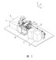
請參閱圖1,本發明實施例中用以剝折的晶片為一矩形的片狀晶片A,其上被規劃具有一矩形區域且表面具積層電鍍層的電阻部位A1,依進行剝折成條狀的剝折順序,該電阻部位A1之X軸向前端形成一段無積層電鍍層的廢料部A2,該電阻部位A1之X軸向後端形成一段無積層電鍍層的夾持部A3,該電阻部位A1之Y軸向兩側分別各形成一段較廢料部A2、夾持部A3狹窄的無積層電鍍層的側邊部A4 、A5;其中,在本發明實施例中,使該側邊部A4、A5分別各區分出包括靠該電阻部位A1的內側邊A41、A51,以及靠電阻部位A1外側的外側邊A42、A52;其中,該外側邊A42、A52包括電阻部位A1、廢料部A2、夾持部A3的邊側部份,而該內側邊A41、A51則僅包括該電阻部位A1的邊側部份;各部位間的分界係如圖1、2所示地分別各在該片狀晶片A下表面刻劃有凹溝狀的線痕A6,該電阻部位A1的下表面劃的線痕A6則呈矩陣排列的矩形格狀(圖中未示),每一矩形格為一電阻元件,未來將剝折成格粒狀的電阻元件。Please refer to FIG. 1. The wafer used for peeling in the embodiment of the present invention is a rectangular sheet-shaped wafer A, which is planned to have a rectangular area and a resistance portion A1 with a layered plating layer on the surface, which is peeled into strips according to In the shape of stripping sequence, the X-axis front end of the resistance part A1 forms a scrap part A2 without build-up plating layer, the X-axis rear end of the resistance part A1 forms a gripping part A3 without build-up plating layer, the resistor The two sides of the portion A1 in the Y-axis direction are respectively formed with a side portion A4 and A5 that are narrower than the scrap portion A2 and the clamping portion A3 and have no build-up plating layer; in the embodiment of the present invention, the side portion A4 is made , A5 are respectively distinguished to include the inner side A41, A51 of the resistance part A1, and the outer side A42, A52 of the resistance part A1 outside; wherein, the outer side A42, A52 includes the resistance part A1, the waste part A2, the side portion of the clamping portion A3, and the inner sides A41, A51 only include the side portion of the resistance portion A1; the boundary between the parts is as shown in Figures 1 and 2 respectively The lower surface of the chip wafer A is engraved with groove-shaped line marks A6, and the line marks A6 on the lower surface of the resistance portion A1 are in the form of rectangular grids arranged in a matrix (not shown in the figure), and each rectangular grid is A resistance element will be stripped into a grid-shaped resistance element in the future.
請參閱圖3、4,在進行剝折成條狀晶片A8前,本發明實施例先執行一將該片狀晶片A的該外側邊A42、A52及該廢料部A2列為待剝除部位,並執行一折邊剝除該待剝除部位的程序,使該片狀晶片A剝折該待剝除部位後,該片狀晶片A形成一僅包括該電阻部位A1、夾持部A3及內側邊A41、A51的待剝條晶片A7; 本發明實施例中之晶片剝折製程係將該待剝條晶片A7剝折成其上包括有一部份該電阻部位A1連同其二內側邊A41、A51條狀區域部位的條狀晶片A8。Please refer to FIGS. 3 and 4. Before stripping into the strip wafer A8, the embodiment of the present invention first executes the outer edges A42 and A52 of the chip wafer A and the scrap part A2 as the parts to be stripped , And execute a procedure of peeling off the part to be stripped by folding, so that the chip wafer A strips the part to be stripped, the chip wafer A forms a part including only the resistance part A1, the clamping part A3 and Strip wafer A7 on the inner side A41, A51; the wafer stripping process in the embodiment of the present invention is to strip the wafer A7 on the strip to be stripped to include a part of the resistance portion A1 together with the two inner sides A41, A51 Strip wafer A8 in the strip region.
請參閱圖4、5,本發明實施例可以圖中所示的堆疊機來作說明,該堆疊機為一進行晶片剝折製程的設備,其設有一剝折機構B,在該待剝條晶片A7被送入該剝折機構B進行剝折成該條狀晶片A8前,該片狀晶片A係置於一置料機構C中,並被一搬送機構D的一提座D1提取並移送至一折邊機構E中,並在該折邊機構E中將該片狀晶片A的剝折成該待剝條晶片A7後,再由該搬送機構D的該提座D1將該待剝條晶片A7移送並越經該折邊機構E,而置於該剝折機構B的該擺座B1進行剝折成該條狀晶片A8;而完成剝折的該條狀晶片A8則被送至一收集裝置F中的一料框F1中受收集。Please refer to FIGS. 4 and 5. The embodiment of the present invention can be illustrated by the stacker shown in the figure. The stacker is a device for performing a wafer peeling process, which is provided with a peeling mechanism B, which is used to strip wafers Before A7 is fed into the stripping mechanism B to be stripped into the strip-shaped wafer A8, the wafer-shaped wafer A is placed in a stocking mechanism C, and is extracted and transferred to a lifting seat D1 of a transport mechanism D to In a hemming mechanism E, and in the hemming mechanism E, the sheet wafer A is stripped into the to-be-stripped wafer A7, and then the to-be-stripped wafer is transported by the carrier D1 of the transport mechanism D A7 transfers and passes the hemming mechanism E, and the pendulum B1 placed in the debonding mechanism B is stripped into the strip wafer A8; and the stripped wafer A8 after the stripping is sent to a collection Collected in a frame F1 in device F.
請參閱圖4、6,該剝折機構B包括:一擺座B1及依待剝折晶片A7在擺座B1上的輸送方向為位於該擺座B1後端可作前後位移的一推夾B2,該擺座B1以兩側的二樞臂B11、B12分別各藉一樞軸部B111共同樞設於一載座B3兩側的二側座B31上,二樞臂B11、B12間設有一供該待剝條晶片A7置於其中並可被一推送機構G的一推夾G1推送的輸送道B13;該載座B3下方受立設於一底座B32上的一旁側座B33及一後側座B34所架高,該擺座B1下方的該底座B32上設有一料盒B4供盛放該待剝條晶片A7被剝剩掉落的該支持部A3;該擺座B1的該輸送道B13前端設一定位裝置H,該擺座B1受以驅動件B5驅動的一偏心輪B6連動一連桿B7而帶動該擺座B1作上、下擺動。Please refer to FIGS. 4 and 6, the peeling mechanism B includes: a swing base B1 and a pushing clip B2 that can be moved back and forth at the rear end of the swing base B1 according to the transport direction of the wafer A7 to be peeled off on the swing base B1 The swing seat B1 is pivotally mounted on the two side seats B31 on both sides of a carrier B3 with two pivot arms B11 and B12 on both sides respectively via a pivot portion B111. A supply is provided between the two pivot arms B11 and B12 The wafer A7 to be stripped is placed in a conveying path B13 which can be pushed by a pushing clip G1 of a pushing mechanism G; a side seat B33 and a rear seat are erected on a base B32 under the carrier B3 Elevated by B34, a box B4 is provided on the base B32 under the swing seat B1 for holding the supporting portion A3 where the wafer A7 to be stripped is dropped; the front end of the conveying path B13 of the swing seat B1 A positioning device H is provided. The swing base B1 is driven by an eccentric wheel B6 driven by a driving member B5 to link a connecting rod B7 to drive the swing base B1 to swing up and down.
請參閱圖4、6、7,該定位裝置H設有:一上定位機構H1及一下定位機構H2,其中: 該上定位機構H1,設有受一驅動件H11驅動可作上、下位移的一壓模H12;該下定位機構H2設有一固設定位之模座H21,該模座H21設有一段寬度與該條狀晶片A8的X軸向寬度約略相當之定位部H211;該條狀晶片A8的Y軸向長度較該模座H21及定位部H211長,而使該條狀晶片A8的該內側邊A41、A51外露於該模座H21及定位部H211的兩側之外; 該待剝條晶片A7置於該擺座B1後,使該待剝條晶片A7後端的該夾持部A3受該推夾G1夾持,經該擺座B1的該輸送道B13沿一直線推送流路向前推送,直到該待剝條晶片A7前端被拘束限制在該定位裝置H之該定位部H211上方與該壓模H12底面間作定位,並藉受該偏心輪B6驅動該連桿B7帶動該擺座B1作上、下擺動,使待剝條晶片A7受該定位裝置H定位的部份被剝折成該條狀晶片A8,剝折後的該條狀晶片A8則留置於該定位部H211上方與該壓模H12底面間,然後再被搬送收集。Please refer to FIGS. 4, 6, and 7, the positioning device H is provided with: an upper positioning mechanism H1 and a lower positioning mechanism H2, wherein: the upper positioning mechanism H1 is provided with a driving member H11 that can be moved up and down A stamper H12; the lower positioning mechanism H2 is provided with a fixed-position die holder H21, the die holder H21 is provided with a positioning portion H211 whose width is approximately equivalent to the X-axis width of the strip wafer A8; the strip wafer The Y axial length of A8 is longer than that of the mold base H21 and the positioning portion H211, so that the inside edges A41 and A51 of the strip wafer A8 are exposed outside the mold base H21 and the positioning portion H211 on both sides; After the stripping wafer A7 is placed on the swing seat B1, the clamping part A3 at the rear end of the strip wafer A7 to be stripped is clamped by the push clip G1, and the conveying path B13 of the swing seat B1 pushes the flow path forward along a straight line Push until the front end of the wafer A7 to be stripped is constrained and restricted between the positioning part H211 of the positioning device H and the bottom surface of the stamper H12, and the eccentric wheel B6 drives the connecting rod B7 to drive the swing seat B1 swings up and down, so that the portion of the wafer A7 to be stripped by the positioning device H is stripped into the strip-shaped wafer A8, and the strip-shaped wafer A8 after the stripping is left above the positioning portion H211 and The bottom surface of the stamper H12 is then transported and collected.
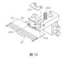
請參閱圖8,該擺座B1一側的一樞臂B12內側設有一第一滑軌B121,該第一滑軌B121上設有一第一滑座B122;該推送機構G設有: 該推夾G1,其呈X軸向設置,包括一底座G11及位於該底座G11上方的壓夾G12,該推夾G1以該底座G11一側固設於一固定座G2的一側; 一緩衝組件G3,包括一滑軌座G31,該滑軌座G31一側設有X軸向的一第二滑軌G32,該第二滑軌G32上設有一第二滑座G321;該滑軌座G31後端固設一Y軸向的止擋部G33,該固定座G2與該止擋部G33間設有一彈簧構成的彈性元件G21;固設該推夾G1的該固定座G2以另一側固設於第二滑座G321上,使該推夾G1可在以該固定座G2在該第二滑軌G32上作X軸向位移;該滑軌座G31下方受一驅動件G4驅動一皮帶G41所連動,使該緩衝組件G3可承載該推夾G1在該第一滑軌B121上作X軸向位移;該彈性元件G21可以在該推夾G1後退時獲得緩衝;該止擋部G33一側並設有一X軸向凸伸的一感應片G331,該感應片G331可受該固定座G2上一感應器G22所感應。Please refer to FIG. 8, a first slide rail B121 is provided inside a pivot arm B12 on one side of the swing seat B1, and a first slide seat B122 is provided on the first slide rail B121; the push mechanism G is provided with: the push clip G1, which is arranged in the X-axis direction, includes a base G11 and a pressing clamp G12 located above the base G11, the push clamp G1 is fixed on one side of a fixed seat G2 with one side of the base G11; a buffer assembly G3, It includes a sliding rail seat G31, a side of the sliding rail seat G31 is provided with a second sliding rail G32 in the X axis direction, the second sliding rail G32 is provided with a second sliding seat G321; the rear end of the sliding rail seat G31 is fixed A stop portion G33 in the Y-axis direction is provided, and an elastic element G21 composed of a spring is provided between the fixing seat G2 and the stop portion G33; the fixing seat G2 fixing the push clip G1 is fixed on the other side on the second side On the two slide seats G321, the push clip G1 can be displaced in the X-axis direction on the second slide rail G32 by the fixing seat G2; under the slide rail seat G31, a driving member G4 drives a belt G41 to move, The buffer assembly G3 can carry the push clip G1 to perform X-axis displacement on the first slide rail B121; the elastic element G21 can obtain a buffer when the push clip G1 is retracted; the stopper G33 side is provided with a A sensing piece G331 protruding in the X axis, the sensing piece G331 can be sensed by a sensor G22 on the fixing base G2.
請參閱圖8〜10, 該推夾G1呈X軸向設置,該底座G11上表面設有一凹設之樞槽G111,該壓夾G12以一樞接部G121樞設於該樞槽G111中一Y軸向的軸桿G112,使該壓夾G12以該樞接部G121為界分為位於前端之壓夾部G122及位於後端的扳動部G123,其中,該扳動部G123受該底座G11下方一驅動件G13所驅動伸經該底座G11上一鏤孔G113的驅動桿G131所作Z軸向的下拉、上頂連動,使位於該樞接部G121另一端之該壓夾部G122前端一壓抵緣G124可作上、下位移,該驅動件G13以驅動桿G131作Z軸向的下拉、上頂連動,可以縮短整個推送機構G的X軸向長度,使其位移時輕省迅速;該底座G11與該扳動部G123間的該鏤孔G113與該樞槽G111間設有一彈性元件G114,可提供該驅動件G13以該驅動桿G131下拉該扳動部G123時的彈性回復力,以控制該壓夾部G122前端的該壓抵緣G124隨時保持一向下壓夾的下壓施力。Please refer to FIGS. 8 to 10, the push clip G1 is arranged in the X-axis direction, the upper surface of the base G11 is provided with a concave pivot groove G111, and the pressing clip G12 is pivotally disposed in the pivot groove G111 with a pivot portion G121 The shaft G112 in the Y axis makes the clamping clamp G12 divided into the clamping clamp G122 at the front end and the pulling portion G123 at the rear end using the pivot portion G121 as the boundary, wherein the pulling portion G123 is received by the base G11 The driving rod G131 driven by a drive hole G113 on the base G11 is driven by a lower driving member G13 to pull down and top in the Z axis, so that the front end of the clamping part G122 at the other end of the pivoting part G121 is pressed The abutment G124 can be moved up and down. The driving member G13 uses the driving rod G131 to pull down and up the Z axis, which can shorten the X axial length of the entire pushing mechanism G, so that the displacement is light and rapid; the An elastic element G114 is provided between the hole G113 and the pivot groove G111 between the base G11 and the pulling part G123, which can provide the elastic restoring force of the driving part G13 when the driving part G123 pulls down the pulling part G123, to The pressing edge G124 at the front end of the clamping part G122 is controlled to maintain a downward pressing force at any time.
請參閱圖9、10,該壓抵緣G124下方的該底座G11上設有一抵座G14,該抵座G14設於該底座G11前端一凹設的區間G115上,並受固設於該區間G115上方之該底座G11上的一壓片G15所壓覆並限制其上移;該抵座G14係以一Z軸向立設的圓形截面樞軸G16 為旋轉中心,而可在水平面以X軸向為中心軸作左右擺動一α角地設於該區間G115之底表面G116上;該抵座G14前端凸設一恰對應於該壓夾部G122前端該壓抵緣G124下方的鉆部G141,該鉆部G141與該樞軸G16間的該鉆部G141兩側分別各設有一Z軸向凸設的圓形截面的擋體G17,兩側的二擋體G17朝前弧形前端的抵緣G171間之連線,在該抵座G14未擺動時係在同一Y軸向直線上,並與通過該樞軸G16中心的X軸向軸線垂直;該二擋體G17的抵緣G171供該推夾G1前移時抵靠該待剝條晶片A7的夾持部A3的後端側緣A31,此時該夾持部A3恰可受壓抵緣G124下壓時夾持於該壓抵緣G124與該鉆部G141間;而藉該抵座G14在該樞軸G16樞設的可左右擺動設計,當該待剝條晶片A7係呈不正之偏擺狀態而使該後端側緣A31僅受其中一擋體G17的抵緣G171抵觸時,可以藉擺動來自動導正該抵座G14,使一擋體G17的抵緣G171抵觸狀態可以轉為二擋體G17的二抵緣G171共同抵觸該後端側緣A31,並以均衡的施力推送該待剝條晶片A7。Please refer to FIGS. 9 and 10. The base G11 under the pressing edge G124 is provided with an abutment seat G14. The abutment seat G14 is provided on a recessed section G115 at the front end of the base G11 and is fixedly fixed in the section G115 A pressing piece G15 on the upper base G11 is pressed and limited to move upwards; the abutment G14 is based on a circular cross-section pivot G16 standing upright in the Z axis as the rotation center, and can be on the horizontal plane with the X axis The center axis is oscillated at an angle of α to the bottom surface G116 of the interval G115; the front end of the abutment seat G14 protrudes a drill portion G141 corresponding to the front end of the pressure clamping portion G122 under the pressure abutment edge G124, the Between the drill portion G141 and the pivot G16, two sides of the drill portion G141 are respectively provided with a circular cross-section stopper G17 protruding in the Z-axis direction, and the two stoppers G17 on both sides face the abutting edge G171 of the forward arc-shaped front end The connecting line is on the same Y-axis straight line when the abutment G14 is not swinging, and is perpendicular to the X-axis axis passing through the center of the pivot G16; the abutment edge G171 of the second stopper G17 is for the push clip When G1 moves forward, it abuts against the rear edge A31 of the clamping portion A3 of the wafer A7 to be stripped. At this time, the clamping portion A3 can be clamped by the pressing edge G124 and the pressing edge G124 Between the drill parts G141; and by the abutment G14 pivotable design on the pivot G16, when the wafer A7 to be stripped is in an irregular deflection state, the rear edge A31 is only affected by it When the abutment G171 of a blocking body G17 collides, the abutment G14 can be automatically guided by swinging, so that the abutment state of the abutment G171 of the one blocking body G17 can be changed to the second abutment G171 of the second blocking body G17 to jointly collide End edge A31, and push the wafer A7 to be stripped with a balanced force.
綜上所述,本發明實施例由於在將該片狀晶片A置入該剝折機構B的擺座B1之輸送道B2前,先執行一折邊剝除該待剝除部位的程序,使該片狀晶片A剝折該待剝除部位後,該片狀晶片A形成一僅包括該電阻部位A1、夾持部A3及內側邊A41、A51的待剝條晶片A7,由於該折邊剝除係依該片狀晶片A下表面刻劃的凹溝狀線痕A6所執行,故折邊剝除待剝除部位後所剩的該待剝條晶片A7具有較正確的矩形,當該推送機構G進行推送時,該待剝條晶片A7可以更平穩而滑順的被推送,使阻涉、歪斜、卡料情形降低,高效率的生產可以更確實的執行;另外,使該緩衝組件G3可承載該推夾G1在該第一滑軌B121上作X軸向位移,而該驅動件G4驅動一皮帶G41連動該滑軌座G31,使推夾G1推料後的後退緩衝更順暢;而驅動該推夾G1的扳動部G123之驅動件G13以由該底座G11下方伸經該底座G11上該鏤孔G113的驅動桿G131作Z軸向的下拉、上頂連動,可以縮短整個推送機構G的X軸向長度,使其位移時輕省迅速,增加推送的順暢性;又,該抵座G14可以樞軸G16 為旋轉中心作左右擺動,可以均衡的施力推送該待剝條晶片A7,使推送更順暢。In summary, in the embodiment of the present invention, before placing the chip wafer A into the conveying path B2 of the swing seat B1 of the peeling mechanism B, a procedure of peeling off the portion to be peeled off is performed by a folding process, so that After the sheet wafer A peels off the portion to be peeled, the sheet wafer A forms a wafer A7 to be stripped including only the resistance portion A1, the clamping portion A3 and the inner sides A41, A51. The stripping is performed according to the groove-shaped line marks A6 scored on the lower surface of the wafer A, so the wafer A7 to be stripped remaining after the edge stripping strips the stripped portion to be stripped has a more correct rectangle. When the pushing mechanism G pushes, the wafer A7 to be stripped can be pushed more smoothly and smoothly, so that the situation of obstruction, skew, and jamming is reduced, and high-efficiency production can be more reliably performed; in addition, the buffer assembly G3 can carry the push clip G1 to perform X-axis displacement on the first slide rail B121, and the driving member G4 drives a belt G41 to interlock the slide rail seat G31, so that the back buffer after the push clip G1 is pushed is smoother; The driving member G13 driving the pulling part G123 of the push clip G1 is extended from below the base G11 through the driving rod G131 of the hole G113 on the base G11 for Z-axis downward and upward linkage, which can shorten the entire push The X-axis length of the mechanism G makes it easy to displace during displacement and increase the smoothness of pushing; in addition, the abutment G14 can pivot left and right with the pivot G16 as the center of rotation, which can push the wafer to be stripped with a balanced force A7, make the push more smooth.
惟以上所述者,僅為本發明之較佳實施例而已,當不能以此 限定本發明實施之範圍,即大凡依本發明申請專利範圍及發明說明內容所作之簡單的等效變化與修飾,皆仍屬本發明專利涵蓋之範圍內。However, the above are only the preferred embodiments of the present invention, which should not be used to limit the scope of the implementation of the present invention, that is, simple equivalent changes and modifications made according to the scope of the patent application of the present invention and the description of the invention, All of them are still covered by the patent of the present invention.
A:片狀晶片A1:電阻部位A2:廢料部A3:夾持部A4:側邊部A41:內側邊A42:外側邊A5:側邊部A51:內側邊A52:外側邊A6:線痕A7:待剝條晶片A8:條狀晶片B:剝折機構B1:擺座B11:樞臂B111:樞軸部B12:樞臂B121:第一滑軌B122:第一滑座B13:輸送道B2:推夾B3:載座B31:側座B32:底座B33:旁側座B34:後側座B4:料盒B5:驅動件B6:偏心輪B7:連桿C:置料機構D:搬送機構D1:提座E:折邊機構F:收集裝置F1:料框G:推夾機構G1:推夾G11:底座G111:樞槽G112:軸桿G113:鏤孔G114:彈性元件G115:區間G116:底表面G12:壓夾G121:樞接部G122:壓夾部G123:扳動部G124:壓抵緣G13:驅動件G131:驅動桿G14:抵座G141:鉆部G15:壓片G16:樞軸G17:擋體G171:抵緣G2:固定座G21:彈性元件G22:感應器G3:緩衝組件G31:滑軌座G32:第二滑軌G321:第二滑座G33:止擋部G331:感應片G4:驅動件G41:皮帶H:定位裝置H1:上定位機構H11:驅動件H12:壓模H2:下定位機構H21:模座H211:定位部A: Chip wafer A1: Resistor part A2: Scrap part A3: Clamping part A4: Side part A41: Inside side A42: Outside side A5: Side side part A51: Inside side A52: Outside side A6: Line mark A7: Strip wafer to be peeled A8: Strip wafer B: Stripping mechanism B1: Swing seat B11: Pivot arm B111: Pivot part B12: Pivot arm B121: First slide rail B122: First slide seat B13: Transport Lane B2: Push clip B3: Carrier B31: Side seat B32: Base B33: Side seat B34: Rear seat B4: Material box B5: Drive part B6: Eccentric wheel B7: Connecting rod C: Feeding mechanism D: Transport Mechanism D1: Lifting seat E: Folding mechanism F: Collecting device F1: Material frame G: Push clamp mechanism G1: Push clamp G11: Base G111: Pivot groove G112: Shaft G113: Slotted G114: Elastic element G115: Section G116 : Bottom surface G12: Clamping G121: Pivoting part G122: Clamping part G123: Pulling part G124: Pressing abutment G13: Driver G131: Driving rod G14: Abutment G141: Drill part G15: Pressing piece G16: Pivot Axis G17: Stopper G171: Abutment G2: Fixed seat G21: Elastic element G22: Sensor G3: Buffer assembly G31: Slide rail seat G32: Second slide rail G321: Second slide seat G33: Stopper G331: Induction Sheet G4: driving part G41: belt H: positioning device H1: upper positioning mechanism H11: driving part H12: stamper H2: lower positioning mechanism H21: mold base H211: positioning part
圖1係本發明實施例中片狀晶片之立體示意圖。 圖2係本發明實施例中片狀晶片部份放大之立體示意圖。 圖3係本發明實施例中片狀晶片之立體分解示意圖。 圖4係本發明實施例中待剝條晶片之立體分解示意圖。 圖5係本發明實施例中晶片剝折製程的設備立體示意圖。 圖6係本發明實施例中剝折機構之立體示意圖。 圖7係本發明實施例中定位裝置之立體分解示意圖。 圖8係本發明實施例中推送裝置與擺座組構關係之立體示意圖。 圖9係本發明實施例中推夾之立體示意圖。 圖10係本發明實施例中推夾對待剝折晶片操作之示意圖。FIG. 1 is a schematic perspective view of a chip wafer in an embodiment of the present invention. FIG. 2 is an enlarged schematic perspective view of a portion of a chip wafer in an embodiment of the present invention. FIG. 3 is a three-dimensional exploded schematic view of a chip wafer in an embodiment of the present invention. FIG. 4 is a three-dimensional exploded schematic view of a wafer to be stripped in an embodiment of the present invention. FIG. 5 is a schematic perspective view of equipment in a wafer peeling process in an embodiment of the present invention. 6 is a perspective schematic view of a peeling mechanism in an embodiment of the present invention. 7 is an exploded perspective view of the positioning device in the embodiment of the present invention. 8 is a three-dimensional schematic diagram of the structure relationship between the pushing device and the swing seat in the embodiment of the present invention. 9 is a perspective schematic view of the push clip in the embodiment of the present invention. FIG. 10 is a schematic diagram of the operation of pushing the wafer to be peeled off in the embodiment of the present invention.
B1:擺座B1: Swing seat
B12:樞臂B12: pivot arm
B121:第一滑軌B121: the first slide
B122:第一滑座B122: The first slide
G:推夾機構G: Push clip mechanism
G1:推夾G1: Push clip
G2:固定座G2: fixed seat
G21:彈性元件G21: elastic element
G22:感應器G22: sensor
G3:緩衝組件G3: Buffer component
G31:滑軌座G31: Slide rail seat
G32:第二滑軌G32: second rail
G321:第二滑座G321: second slide
G33:止擋部G33: stop
G331:感應片G331: Induction film
G4:驅動件G4: driver
G41:皮帶G41: belt
Claims (11)
Translated fromChinesePriority Applications (3)
| Application Number | Priority Date | Filing Date | Title |
|---|---|---|---|
| TW107137380ATWI683383B (en) | 2018-10-23 | 2018-10-23 | Pushing method and mechanism of wafer stripping process and equipment using the mechanism |
| CN201821853355.5UCN209087781U (en) | 2018-10-23 | 2018-11-12 | Chip stripping and folding process sheet chip, chip to be stripped and folded, pushing mechanism and equipment |
| CN201811337281.4ACN111086880A (en) | 2018-10-23 | 2018-11-12 | Pushing method and mechanism for chip peeling and folding process and equipment using the same |
Applications Claiming Priority (1)
| Application Number | Priority Date | Filing Date | Title |
|---|---|---|---|
| TW107137380ATWI683383B (en) | 2018-10-23 | 2018-10-23 | Pushing method and mechanism of wafer stripping process and equipment using the mechanism |
Publications (2)
| Publication Number | Publication Date |
|---|---|
| TWI683383B TWI683383B (en) | 2020-01-21 |
| TW202017073Atrue TW202017073A (en) | 2020-05-01 |
Family
ID=67123475
Family Applications (1)
| Application Number | Title | Priority Date | Filing Date |
|---|---|---|---|
| TW107137380ATWI683383B (en) | 2018-10-23 | 2018-10-23 | Pushing method and mechanism of wafer stripping process and equipment using the mechanism |
Country Status (2)
| Country | Link |
|---|---|
| CN (2) | CN209087781U (en) |
| TW (1) | TWI683383B (en) |
Families Citing this family (2)
| Publication number | Priority date | Publication date | Assignee | Title |
|---|---|---|---|---|
| TWI683383B (en)* | 2018-10-23 | 2020-01-21 | 萬潤科技股份有限公司 | Pushing method and mechanism of wafer stripping process and equipment using the mechanism |
| CN119601511B (en)* | 2025-02-10 | 2025-04-15 | 浙江中晶新材料研究有限公司 | A silicon wafer edge efficient peeling device and method |
Family Cites Families (11)
| Publication number | Priority date | Publication date | Assignee | Title |
|---|---|---|---|---|
| TW314065U (en)* | 1997-01-14 | 1997-08-21 | Yageo Corp | Chip resistor stripping, arranging, and aligning machine |
| CN2580488Y (en)* | 2002-08-29 | 2003-10-15 | 上海金亭汽车线束有限公司 | Line pencil automatic locking device |
| TW201213571A (en)* | 2010-09-17 | 2012-04-01 | Beer Corp | Preparation method of on-chip passive component |
| CN202464262U (en)* | 2012-02-06 | 2012-10-03 | 昆山华拓电子科技有限公司 | Chip resistor strip bending machine |
| CN202839187U (en)* | 2012-07-13 | 2013-03-27 | 万润科技精机(昆山)有限公司 | Stripping device for chip |
| CN202839559U (en)* | 2012-07-13 | 2013-03-27 | 万润科技精机(昆山)有限公司 | Chip collecting device |
| CN205928005U (en)* | 2016-08-24 | 2017-02-08 | 安徽省青阳县华瑞科技有限公司 | Bearing frame adds clamping apparatus |
| CN206288699U (en)* | 2016-11-25 | 2017-06-30 | 上汽通用五菱汽车股份有限公司 | A kind of feeding device of special-shaped glass coating system |
| CN207367714U (en)* | 2017-09-22 | 2018-05-15 | 昆山市和博电子科技有限公司 | A kind of automatic folded plate system |
| CN207551309U (en)* | 2017-10-18 | 2018-06-29 | 迅得机械(东莞)有限公司 | a feeding mechanism |
| TWI683383B (en)* | 2018-10-23 | 2020-01-21 | 萬潤科技股份有限公司 | Pushing method and mechanism of wafer stripping process and equipment using the mechanism |
- 2018
- 2018-10-23TWTW107137380Apatent/TWI683383B/ennot_activeIP Right Cessation
- 2018-11-12CNCN201821853355.5Upatent/CN209087781U/ennot_activeExpired - Fee Related
- 2018-11-12CNCN201811337281.4Apatent/CN111086880A/ennot_activeWithdrawn
Also Published As
| Publication number | Publication date |
|---|---|
| CN209087781U (en) | 2019-07-09 |
| CN111086880A (en) | 2020-05-01 |
| TWI683383B (en) | 2020-01-21 |
Similar Documents
| Publication | Publication Date | Title |
|---|---|---|
| WO2022121168A1 (en) | Film tearing and pressure maintaining integrated assembly line | |
| CN108163310A (en) | An automatic labeling machine | |
| TWI683383B (en) | Pushing method and mechanism of wafer stripping process and equipment using the mechanism | |
| CN110884938A (en) | Adhesive tape cutting and sticking equipment | |
| KR100770411B1 (en) | Coverlay attachment system and method | |
| CN211056323U (en) | Transfer mechanism and cutting and conveying device | |
| CN206446838U (en) | Fully automatic mobile phone glass seed film machine | |
| JPS60168148A (en) | Printing machine | |
| CN111233341A (en) | Automatic auxiliary line for automatic film coating | |
| CN214221722U (en) | Attachment placement machine | |
| TW201808756A (en) | Tray assembly and device for transporting tray assembly, and method and device for picking components from tray assembly includes a tray assembly for placing a plurality of first components to be processed in a matrix arrangement | |
| CN211310366U (en) | Adhesive tape cutting and sticking equipment | |
| CN216139669U (en) | A circulating gripper mechanism and high-speed automatic magnetic printing machine | |
| CN215325967U (en) | Label preparation all-in-one | |
| CN110125637A (en) | A kind of magnetic adsorption plate shifting apparatus | |
| CN205708990U (en) | Automatic feeding equipment for screen printing machines | |
| CN116424674A (en) | Full-automatic film tearing machine and film tearing process thereof | |
| CN204384581U (en) | A kind of taping apparatus | |
| CN114803276A (en) | Send button device and send button machine | |
| CN211031394U (en) | Paper box forming transfer device | |
| TWI579220B (en) | Method and device for component extraction of fitting process | |
| CN212402649U (en) | Grabbing and placing mechanism of film inserting machine | |
| CN223253920U (en) | Material transfer device and material assembly system | |
| CN222869145U (en) | Board breaking device | |
| TWI683389B (en) | Method and device for conveying wafer peeling process and equipment using the same |
Legal Events
| Date | Code | Title | Description |
|---|---|---|---|
| MM4A | Annulment or lapse of patent due to non-payment of fees |