TW202013693A - Semiconductor device, display device including the semiconductor device, display module including the display device, and electronic device including the semiconductor device, the display device, and the display module - Google Patents
Semiconductor device, display device including the semiconductor device, display module including the display device, and electronic device including the semiconductor device, the display device, and the display moduleDownload PDFInfo
- Publication number
- TW202013693A TW202013693ATW108126104ATW108126104ATW202013693ATW 202013693 ATW202013693 ATW 202013693ATW 108126104 ATW108126104 ATW 108126104ATW 108126104 ATW108126104 ATW 108126104ATW 202013693 ATW202013693 ATW 202013693A
- Authority
- TW
- Taiwan
- Prior art keywords
- film
- insulating film
- conductive film
- oxide semiconductor
- transistor
- Prior art date
Links
- 239000004065semiconductorSubstances0.000titleclaimsabstractdescription437
- 239000003990capacitorSubstances0.000abstractdescription74
- 239000010408filmSubstances0.000description1762
- 239000000758substrateSubstances0.000description185
- 229910052760oxygenInorganic materials0.000description143
- 239000001301oxygenSubstances0.000description141
- QVGXLLKOCUKJST-UHFFFAOYSA-Natomic oxygenChemical compound[O]QVGXLLKOCUKJST-UHFFFAOYSA-N0.000description137
- 238000000034methodMethods0.000description136
- 239000010410layerSubstances0.000description129
- 239000013078crystalSubstances0.000description104
- 239000007789gasSubstances0.000description100
- 239000002245particleSubstances0.000description81
- XKRFYHLGVUSROY-UHFFFAOYSA-NArgonChemical compound[Ar]XKRFYHLGVUSROY-UHFFFAOYSA-N0.000description70
- 239000012535impuritySubstances0.000description70
- IJGRMHOSHXDMSA-UHFFFAOYSA-NAtomic nitrogenChemical compoundN#NIJGRMHOSHXDMSA-UHFFFAOYSA-N0.000description62
- 230000006870functionEffects0.000description61
- XUIMIQQOPSSXEZ-UHFFFAOYSA-NSiliconChemical compound[Si]XUIMIQQOPSSXEZ-UHFFFAOYSA-N0.000description58
- 125000004429atomChemical group0.000description58
- 229910052710siliconInorganic materials0.000description58
- 239000010703siliconSubstances0.000description58
- 239000004973liquid crystal related substanceSubstances0.000description56
- 230000007547defectEffects0.000description54
- 238000010438heat treatmentMethods0.000description52
- 238000010586diagramMethods0.000description42
- 239000011701zincSubstances0.000description42
- 229910052739hydrogenInorganic materials0.000description40
- 239000004020conductorSubstances0.000description37
- 229910052786argonInorganic materials0.000description36
- 230000008569processEffects0.000description36
- 238000004544sputter depositionMethods0.000description36
- 238000004519manufacturing processMethods0.000description32
- 239000001257hydrogenSubstances0.000description31
- 229910052757nitrogenInorganic materials0.000description31
- 238000003776cleavage reactionMethods0.000description29
- 230000007017scissionEffects0.000description29
- 229910052751metalInorganic materials0.000description28
- 239000000463materialSubstances0.000description26
- MWUXSHHQAYIFBG-UHFFFAOYSA-Nnitrogen oxideInorganic materialsO=[N]MWUXSHHQAYIFBG-UHFFFAOYSA-N0.000description25
- 229910052581Si3N4Inorganic materials0.000description24
- 229910052733galliumInorganic materials0.000description24
- 238000012545processingMethods0.000description24
- HQVNEWCFYHHQES-UHFFFAOYSA-Nsilicon nitrideChemical compoundN12[Si]34N5[Si]62N3[Si]51N64HQVNEWCFYHHQES-UHFFFAOYSA-N0.000description24
- 239000002184metalSubstances0.000description23
- 230000003287optical effectEffects0.000description23
- XLOMVQKBTHCTTD-UHFFFAOYSA-NZinc monoxideChemical compound[Zn]=OXLOMVQKBTHCTTD-UHFFFAOYSA-N0.000description22
- 229910052782aluminiumInorganic materials0.000description22
- XAGFODPZIPBFFR-UHFFFAOYSA-NaluminiumChemical compound[Al]XAGFODPZIPBFFR-UHFFFAOYSA-N0.000description22
- 238000004364calculation methodMethods0.000description22
- GYHNNYVSQQEPJS-UHFFFAOYSA-NGalliumChemical compound[Ga]GYHNNYVSQQEPJS-UHFFFAOYSA-N0.000description20
- 206010021143HypoxiaDiseases0.000description20
- 230000015572biosynthetic processEffects0.000description20
- 239000000126substanceSubstances0.000description20
- 238000003917TEM imageMethods0.000description19
- 238000009413insulationMethods0.000description19
- -1oxygen ionsChemical class0.000description19
- 150000002500ionsChemical class0.000description18
- 229910052721tungstenInorganic materials0.000description18
- 238000006243chemical reactionMethods0.000description17
- 239000010937tungstenSubstances0.000description17
- 150000002431hydrogenChemical class0.000description16
- WFKWXMTUELFFGS-UHFFFAOYSA-NtungstenChemical compound[W]WFKWXMTUELFFGS-UHFFFAOYSA-N0.000description16
- UFHFLCQGNIYNRP-UHFFFAOYSA-NHydrogenChemical compound[H][H]UFHFLCQGNIYNRP-UHFFFAOYSA-N0.000description15
- 229910007541Zn OInorganic materials0.000description15
- 239000012298atmosphereSubstances0.000description15
- 238000005259measurementMethods0.000description15
- VUFNLQXQSDUXKB-DOFZRALJSA-N2-[4-[4-[bis(2-chloroethyl)amino]phenyl]butanoyloxy]ethyl (5z,8z,11z,14z)-icosa-5,8,11,14-tetraenoateChemical compoundCCCCC\C=C/C\C=C/C\C=C/C\C=C/CCCC(=O)OCCOC(=O)CCCC1=CC=C(N(CCCl)CCCl)C=C1VUFNLQXQSDUXKB-DOFZRALJSA-N0.000description14
- GQPLMRYTRLFLPF-UHFFFAOYSA-NNitrous OxideChemical compound[O-][N+]#NGQPLMRYTRLFLPF-UHFFFAOYSA-N0.000description13
- 230000005540biological transmissionEffects0.000description13
- 239000010949copperSubstances0.000description12
- 238000002524electron diffraction dataMethods0.000description12
- 238000000206photolithographyMethods0.000description12
- VYPSYNLAJGMNEJ-UHFFFAOYSA-Nsilicon dioxideInorganic materialsO=[Si]=OVYPSYNLAJGMNEJ-UHFFFAOYSA-N0.000description12
- 239000002356single layerSubstances0.000description12
- MZLGASXMSKOWSE-UHFFFAOYSA-Ntantalum nitrideChemical compound[Ta]#NMZLGASXMSKOWSE-UHFFFAOYSA-N0.000description12
- 239000010409thin filmSubstances0.000description12
- RYGMFSIKBFXOCR-UHFFFAOYSA-NCopperChemical compound[Cu]RYGMFSIKBFXOCR-UHFFFAOYSA-N0.000description11
- 229910052802copperInorganic materials0.000description11
- 238000002003electron diffractionMethods0.000description11
- 239000011521glassSubstances0.000description11
- 150000004767nitridesChemical class0.000description11
- 229910052814silicon oxideInorganic materials0.000description11
- 239000011787zinc oxideSubstances0.000description11
- QGZKDVFQNNGYKY-UHFFFAOYSA-NAmmoniaChemical compoundNQGZKDVFQNNGYKY-UHFFFAOYSA-N0.000description10
- OKTJSMMVPCPJKN-UHFFFAOYSA-NCarbonChemical compound[C]OKTJSMMVPCPJKN-UHFFFAOYSA-N0.000description10
- 238000000231atomic layer depositionMethods0.000description10
- 229910052799carbonInorganic materials0.000description10
- 230000000694effectsEffects0.000description10
- 230000005684electric fieldEffects0.000description10
- 238000005530etchingMethods0.000description10
- 125000004430oxygen atomChemical groupO*0.000description10
- 238000004549pulsed laser depositionMethods0.000description10
- 238000002230thermal chemical vapour depositionMethods0.000description10
- 238000005229chemical vapour depositionMethods0.000description9
- 239000011261inert gasSubstances0.000description9
- 229910044991metal oxideInorganic materials0.000description9
- 150000004706metal oxidesChemical class0.000description9
- 238000005268plasma chemical vapour depositionMethods0.000description9
- 238000005477sputtering targetMethods0.000description9
- 238000003860storageMethods0.000description9
- 229910052725zincInorganic materials0.000description9
- RTAQQCXQSZGOHL-UHFFFAOYSA-NTitaniumChemical compound[Ti]RTAQQCXQSZGOHL-UHFFFAOYSA-N0.000description8
- 230000008859changeEffects0.000description8
- 239000000470constituentSubstances0.000description8
- 230000005012migrationEffects0.000description8
- 238000013508migrationMethods0.000description8
- 230000000149penetrating effectEffects0.000description8
- 239000011347resinSubstances0.000description8
- 229920005989resinPolymers0.000description8
- 229910052719titaniumInorganic materials0.000description8
- 239000010936titaniumSubstances0.000description8
- ZAMOUSCENKQFHK-UHFFFAOYSA-NChlorine atomChemical compound[Cl]ZAMOUSCENKQFHK-UHFFFAOYSA-N0.000description7
- XEEYBQQBJWHFJM-UHFFFAOYSA-NIronChemical compound[Fe]XEEYBQQBJWHFJM-UHFFFAOYSA-N0.000description7
- 230000004913activationEffects0.000description7
- 229910045601alloyInorganic materials0.000description7
- 239000000956alloySubstances0.000description7
- 229910052796boronInorganic materials0.000description7
- 239000000460chlorineSubstances0.000description7
- 229910052801chlorineInorganic materials0.000description7
- 238000000576coating methodMethods0.000description7
- 238000001312dry etchingMethods0.000description7
- 229910052735hafniumInorganic materials0.000description7
- 239000000203mixtureSubstances0.000description7
- 229910052698phosphorusInorganic materials0.000description7
- 239000011574phosphorusSubstances0.000description7
- 238000001004secondary ion mass spectrometryMethods0.000description7
- XLYOFNOQVPJJNP-UHFFFAOYSA-NwaterSubstancesOXLYOFNOQVPJJNP-UHFFFAOYSA-N0.000description7
- 229910001868waterInorganic materials0.000description7
- ZOXJGFHDIHLPTG-UHFFFAOYSA-NBoronChemical compound[B]ZOXJGFHDIHLPTG-UHFFFAOYSA-N0.000description6
- PXGOKWXKJXAPGV-UHFFFAOYSA-NFluorineChemical compoundFFPXGOKWXKJXAPGV-UHFFFAOYSA-N0.000description6
- PXHVJJICTQNCMI-UHFFFAOYSA-NNickelChemical compound[Ni]PXHVJJICTQNCMI-UHFFFAOYSA-N0.000description6
- OAICVXFJPJFONN-UHFFFAOYSA-NPhosphorusChemical compound[P]OAICVXFJPJFONN-UHFFFAOYSA-N0.000description6
- BLRPTPMANUNPDV-UHFFFAOYSA-NSilaneChemical compound[SiH4]BLRPTPMANUNPDV-UHFFFAOYSA-N0.000description6
- 230000001133accelerationEffects0.000description6
- HVYWMOMLDIMFJA-DPAQBDIFSA-NcholesterolChemical compoundC1C=C2C[C@@H](O)CC[C@]2(C)[C@@H]2[C@@H]1[C@@H]1CC[C@H]([C@H](C)CCCC(C)C)[C@@]1(C)CC2HVYWMOMLDIMFJA-DPAQBDIFSA-N0.000description6
- 239000003086colorantSubstances0.000description6
- 230000007423decreaseEffects0.000description6
- 238000000151depositionMethods0.000description6
- 230000008021depositionEffects0.000description6
- 229910052731fluorineInorganic materials0.000description6
- 239000011737fluorineSubstances0.000description6
- 239000007788liquidSubstances0.000description6
- TWNQGVIAIRXVLR-UHFFFAOYSA-Noxo(oxoalumanyloxy)alumaneChemical compoundO=[Al]O[Al]=OTWNQGVIAIRXVLR-UHFFFAOYSA-N0.000description6
- 230000003071parasitic effectEffects0.000description6
- 238000009832plasma treatmentMethods0.000description6
- 229910000077silaneInorganic materials0.000description6
- 239000013077target materialSubstances0.000description6
- HCHKCACWOHOZIP-UHFFFAOYSA-NZincChemical group[Zn]HCHKCACWOHOZIP-UHFFFAOYSA-N0.000description5
- 229910021529ammoniaInorganic materials0.000description5
- 239000002585baseSubstances0.000description5
- 238000002425crystallisationMethods0.000description5
- 230000008025crystallizationEffects0.000description5
- AJNVQOSZGJRYEI-UHFFFAOYSA-Ndigallium;oxygen(2-)Chemical compound[O-2].[O-2].[O-2].[Ga+3].[Ga+3]AJNVQOSZGJRYEI-UHFFFAOYSA-N0.000description5
- 238000010894electron beam technologyMethods0.000description5
- 239000005262ferroelectric liquid crystals (FLCs)Substances0.000description5
- 229910001195gallium oxideInorganic materials0.000description5
- VBJZVLUMGGDVMO-UHFFFAOYSA-Nhafnium atomChemical compound[Hf]VBJZVLUMGGDVMO-UHFFFAOYSA-N0.000description5
- 229910000449hafnium oxideInorganic materials0.000description5
- WIHZLLGSGQNAGK-UHFFFAOYSA-Nhafnium(4+);oxygen(2-)Chemical compound[O-2].[O-2].[Hf+4]WIHZLLGSGQNAGK-UHFFFAOYSA-N0.000description5
- 238000005468ion implantationMethods0.000description5
- 229920001721polyimidePolymers0.000description5
- 238000007789sealingMethods0.000description5
- 239000003566sealing materialSubstances0.000description5
- 229910052709silverInorganic materials0.000description5
- 239000004332silverSubstances0.000description5
- 238000009751slip formingMethods0.000description5
- CURLTUGMZLYLDI-UHFFFAOYSA-NCarbon dioxideChemical compoundO=C=OCURLTUGMZLYLDI-UHFFFAOYSA-N0.000description4
- MYMOFIZGZYHOMD-UHFFFAOYSA-NDioxygenChemical compoundO=OMYMOFIZGZYHOMD-UHFFFAOYSA-N0.000description4
- 230000009471actionEffects0.000description4
- 230000000903blocking effectEffects0.000description4
- 150000001875compoundsChemical class0.000description4
- 229910001882dioxygenInorganic materials0.000description4
- 239000000835fiberSubstances0.000description4
- 238000000731high angular annular dark-field scanning transmission electron microscopyMethods0.000description4
- 229910052738indiumInorganic materials0.000description4
- APFVFJFRJDLVQX-UHFFFAOYSA-Nindium atomChemical group[In]APFVFJFRJDLVQX-UHFFFAOYSA-N0.000description4
- AMGQUBHHOARCQH-UHFFFAOYSA-Nindium;oxotinChemical compound[In].[Sn]=OAMGQUBHHOARCQH-UHFFFAOYSA-N0.000description4
- 229910052742ironInorganic materials0.000description4
- 239000012528membraneSubstances0.000description4
- 239000012299nitrogen atmosphereSubstances0.000description4
- 230000002441reversible effectEffects0.000description4
- 229910052727yttriumInorganic materials0.000description4
- YVTHLONGBIQYBO-UHFFFAOYSA-Nzinc indium(3+) oxygen(2-)Chemical compound[O--].[Zn++].[In+3]YVTHLONGBIQYBO-UHFFFAOYSA-N0.000description4
- UWCWUCKPEYNDNV-LBPRGKRZSA-N2,6-dimethyl-n-[[(2s)-pyrrolidin-2-yl]methyl]anilineChemical compoundCC1=CC=CC(C)=C1NC[C@H]1NCCC1UWCWUCKPEYNDNV-LBPRGKRZSA-N0.000description3
- 229920000178Acrylic resinPolymers0.000description3
- 239000004925Acrylic resinSubstances0.000description3
- VYZAMTAEIAYCRO-UHFFFAOYSA-NChromiumChemical compound[Cr]VYZAMTAEIAYCRO-UHFFFAOYSA-N0.000description3
- ZOKXTWBITQBERF-UHFFFAOYSA-NMolybdenumChemical compound[Mo]ZOKXTWBITQBERF-UHFFFAOYSA-N0.000description3
- 229910052779NeodymiumInorganic materials0.000description3
- 239000004642PolyimideSubstances0.000description3
- 229910052783alkali metalInorganic materials0.000description3
- 150000001340alkali metalsChemical class0.000description3
- 229910052784alkaline earth metalInorganic materials0.000description3
- 150000001342alkaline earth metalsChemical class0.000description3
- 238000004458analytical methodMethods0.000description3
- 235000012000cholesterolNutrition0.000description3
- 229910052804chromiumInorganic materials0.000description3
- 239000011651chromiumSubstances0.000description3
- 239000011248coating agentSubstances0.000description3
- 238000004891communicationMethods0.000description3
- 238000012937correctionMethods0.000description3
- 238000009826distributionMethods0.000description3
- 238000001704evaporationMethods0.000description3
- 239000000284extractSubstances0.000description3
- 229910003437indium oxideInorganic materials0.000description3
- PJXISJQVUVHSOJ-UHFFFAOYSA-Nindium(iii) oxideChemical compound[O-2].[O-2].[O-2].[In+3].[In+3]PJXISJQVUVHSOJ-UHFFFAOYSA-N0.000description3
- 238000010030laminatingMethods0.000description3
- WPBNNNQJVZRUHP-UHFFFAOYSA-Lmanganese(2+);methyl n-[[2-(methoxycarbonylcarbamothioylamino)phenyl]carbamothioyl]carbamate;n-[2-(sulfidocarbothioylamino)ethyl]carbamodithioateChemical compound[Mn+2].[S-]C(=S)NCCNC([S-])=S.COC(=O)NC(=S)NC1=CC=CC=C1NC(=S)NC(=O)OCWPBNNNQJVZRUHP-UHFFFAOYSA-L0.000description3
- 238000002156mixingMethods0.000description3
- 229910052750molybdenumInorganic materials0.000description3
- 239000011733molybdenumSubstances0.000description3
- 239000002159nanocrystalSubstances0.000description3
- 229910052759nickelInorganic materials0.000description3
- 239000001272nitrous oxideSubstances0.000description3
- QGLKJKCYBOYXKC-UHFFFAOYSA-NnonaoxidotritungstenChemical compoundO=[W]1(=O)O[W](=O)(=O)O[W](=O)(=O)O1QGLKJKCYBOYXKC-UHFFFAOYSA-N0.000description3
- 239000007800oxidant agentSubstances0.000description3
- 230000001590oxidative effectEffects0.000description3
- 238000005192partitionMethods0.000description3
- 239000004033plasticSubstances0.000description3
- 229920003023plasticPolymers0.000description3
- BASFCYQUMIYNBI-UHFFFAOYSA-NplatinumSubstances[Pt]BASFCYQUMIYNBI-UHFFFAOYSA-N0.000description3
- 229920000728polyesterPolymers0.000description3
- 230000004044responseEffects0.000description3
- 125000006850spacer groupChemical group0.000description3
- 238000012916structural analysisMethods0.000description3
- 229910052715tantalumInorganic materials0.000description3
- GUVRBAGPIYLISA-UHFFFAOYSA-Ntantalum atomChemical compound[Ta]GUVRBAGPIYLISA-UHFFFAOYSA-N0.000description3
- JBQYATWDVHIOAR-UHFFFAOYSA-NtellanylidenegermaniumChemical compound[Te]=[Ge]JBQYATWDVHIOAR-UHFFFAOYSA-N0.000description3
- 229910052718tinInorganic materials0.000description3
- 238000011282treatmentMethods0.000description3
- 229910001930tungsten oxideInorganic materials0.000description3
- 238000001039wet etchingMethods0.000description3
- 229910052726zirconiumInorganic materials0.000description3
- MGWGWNFMUOTEHG-UHFFFAOYSA-N4-(3,5-dimethylphenyl)-1,3-thiazol-2-amineChemical compoundCC1=CC(C)=CC(C=2N=C(N)SC=2)=C1MGWGWNFMUOTEHG-UHFFFAOYSA-N0.000description2
- 229910052684CeriumInorganic materials0.000description2
- PWHULOQIROXLJO-UHFFFAOYSA-NManganeseChemical compound[Mn]PWHULOQIROXLJO-UHFFFAOYSA-N0.000description2
- BPQQTUXANYXVAA-UHFFFAOYSA-NOrthosilicateChemical compound[O-][Si]([O-])([O-])[O-]BPQQTUXANYXVAA-UHFFFAOYSA-N0.000description2
- CBENFWSGALASAD-UHFFFAOYSA-NOzoneChemical compound[O-][O+]=OCBENFWSGALASAD-UHFFFAOYSA-N0.000description2
- KDLHZDBZIXYQEI-UHFFFAOYSA-NPalladiumChemical compound[Pd]KDLHZDBZIXYQEI-UHFFFAOYSA-N0.000description2
- BOTDANWDWHJENH-UHFFFAOYSA-NTetraethyl orthosilicateChemical compoundCCO[Si](OCC)(OCC)OCCBOTDANWDWHJENH-UHFFFAOYSA-N0.000description2
- ATJFFYVFTNAWJD-UHFFFAOYSA-NTinChemical compound[Sn]ATJFFYVFTNAWJD-UHFFFAOYSA-N0.000description2
- GWEVSGVZZGPLCZ-UHFFFAOYSA-NTitan oxideChemical compoundO=[Ti]=OGWEVSGVZZGPLCZ-UHFFFAOYSA-N0.000description2
- NRTOMJZYCJJWKI-UHFFFAOYSA-NTitanium nitrideChemical compound[Ti]#NNRTOMJZYCJJWKI-UHFFFAOYSA-N0.000description2
- 238000002441X-ray diffractionMethods0.000description2
- 239000002156adsorbateSubstances0.000description2
- 238000000779annular dark-field scanning transmission electron microscopyMethods0.000description2
- 239000004760aramidSubstances0.000description2
- 229920003235aromatic polyamidePolymers0.000description2
- 238000004380ashingMethods0.000description2
- 229910002092carbon dioxideInorganic materials0.000description2
- 239000001569carbon dioxideSubstances0.000description2
- 239000000969carrierSubstances0.000description2
- 229910017052cobaltInorganic materials0.000description2
- 239000010941cobaltSubstances0.000description2
- GUTLYIVDDKVIGB-UHFFFAOYSA-Ncobalt atomChemical compound[Co]GUTLYIVDDKVIGB-UHFFFAOYSA-N0.000description2
- 230000018044dehydrationEffects0.000description2
- 238000006297dehydration reactionMethods0.000description2
- 238000003795desorptionMethods0.000description2
- ZYLGGWPMIDHSEZ-UHFFFAOYSA-Ndimethylazanide;hafnium(4+)Chemical compound[Hf+4].C[N-]C.C[N-]C.C[N-]C.C[N-]CZYLGGWPMIDHSEZ-UHFFFAOYSA-N0.000description2
- 238000001362electron spin resonance spectrumMethods0.000description2
- 230000005281excited stateEffects0.000description2
- 230000001747exhibiting effectEffects0.000description2
- 230000005669field effectEffects0.000description2
- 239000011888foilSubstances0.000description2
- 238000002309gasificationMethods0.000description2
- 239000001307heliumSubstances0.000description2
- 229910052734heliumInorganic materials0.000description2
- SWQJXJOGLNCZEY-UHFFFAOYSA-Nhelium atomChemical compound[He]SWQJXJOGLNCZEY-UHFFFAOYSA-N0.000description2
- 229910052743kryptonInorganic materials0.000description2
- DNNSSWSSYDEUBZ-UHFFFAOYSA-Nkrypton atomChemical compound[Kr]DNNSSWSSYDEUBZ-UHFFFAOYSA-N0.000description2
- 229910052746lanthanumInorganic materials0.000description2
- 229910052748manganeseInorganic materials0.000description2
- 239000011572manganeseSubstances0.000description2
- 239000011159matrix materialSubstances0.000description2
- 239000007769metal materialSubstances0.000description2
- 238000000329molecular dynamics simulationMethods0.000description2
- 229910052754neonInorganic materials0.000description2
- GKAOGPIIYCISHV-UHFFFAOYSA-Nneon atomChemical compound[Ne]GKAOGPIIYCISHV-UHFFFAOYSA-N0.000description2
- JCXJVPUVTGWSNB-UHFFFAOYSA-Nnitrogen dioxideInorganic materialsO=[N]=OJCXJVPUVTGWSNB-UHFFFAOYSA-N0.000description2
- HMMGMWAXVFQUOA-UHFFFAOYSA-NoctamethylcyclotetrasiloxaneChemical compoundC[Si]1(C)O[Si](C)(C)O[Si](C)(C)O[Si](C)(C)O1HMMGMWAXVFQUOA-UHFFFAOYSA-N0.000description2
- 150000002894organic compoundsChemical class0.000description2
- 239000011368organic materialSubstances0.000description2
- 230000003647oxidationEffects0.000description2
- 238000007254oxidation reactionMethods0.000description2
- SIWVEOZUMHYXCS-UHFFFAOYSA-Noxo(oxoyttriooxy)yttriumChemical compoundO=[Y]O[Y]=OSIWVEOZUMHYXCS-UHFFFAOYSA-N0.000description2
- 229920006122polyamide resinPolymers0.000description2
- 229920000139polyethylene terephthalatePolymers0.000description2
- 239000005020polyethylene terephthalateSubstances0.000description2
- 239000002243precursorSubstances0.000description2
- 230000009467reductionEffects0.000description2
- 239000000243solutionSubstances0.000description2
- 239000002904solventSubstances0.000description2
- 238000004611spectroscopical analysisMethods0.000description2
- 239000010935stainless steelSubstances0.000description2
- 229910001220stainless steelInorganic materials0.000description2
- CZDYPVPMEAXLPK-UHFFFAOYSA-NtetramethylsilaneChemical compoundC[Si](C)(C)CCZDYPVPMEAXLPK-UHFFFAOYSA-N0.000description2
- OGIDPMRJRNCKJF-UHFFFAOYSA-Ntitanium oxideInorganic materials[Ti]=OOGIDPMRJRNCKJF-UHFFFAOYSA-N0.000description2
- 238000012546transferMethods0.000description2
- 238000002834transmittanceMethods0.000description2
- JLTRXTDYQLMHGR-UHFFFAOYSA-NtrimethylaluminiumChemical compoundC[Al](C)CJLTRXTDYQLMHGR-UHFFFAOYSA-N0.000description2
- 238000001771vacuum depositionMethods0.000description2
- 229910052724xenonInorganic materials0.000description2
- FHNFHKCVQCLJFQ-UHFFFAOYSA-Nxenon atomChemical compound[Xe]FHNFHKCVQCLJFQ-UHFFFAOYSA-N0.000description2
- 244000025254Cannabis sativaSpecies0.000description1
- 235000012766Cannabis sativa ssp. sativa var. sativaNutrition0.000description1
- 235000012765Cannabis sativa ssp. sativa var. spontaneaNutrition0.000description1
- 229920000298CellophanePolymers0.000description1
- 229920000742CottonPolymers0.000description1
- 229910000881Cu alloyInorganic materials0.000description1
- 239000004593EpoxySubstances0.000description1
- 229910005555GaZnOInorganic materials0.000description1
- 229910004129HfSiOInorganic materials0.000description1
- 239000005264High molar mass liquid crystalSubstances0.000description1
- 229910000846In alloyInorganic materials0.000description1
- FYYHWMGAXLPEAU-UHFFFAOYSA-NMagnesiumChemical compound[Mg]FYYHWMGAXLPEAU-UHFFFAOYSA-N0.000description1
- 229910002089NOxInorganic materials0.000description1
- 239000004677NylonSubstances0.000description1
- 229910001252Pd alloyInorganic materials0.000description1
- 239000004952PolyamideSubstances0.000description1
- 239000004983Polymer Dispersed Liquid CrystalSubstances0.000description1
- 239000004721Polyphenylene oxideSubstances0.000description1
- 239000004743PolypropyleneSubstances0.000description1
- 229920000297RayonPolymers0.000description1
- 239000004990Smectic liquid crystalSubstances0.000description1
- 239000004974Thermotropic liquid crystalSubstances0.000description1
- 239000007983Tris bufferSubstances0.000description1
- QCWXUUIWCKQGHC-UHFFFAOYSA-NZirconiumChemical compound[Zr]QCWXUUIWCKQGHC-UHFFFAOYSA-N0.000description1
- 229910009367Zn MInorganic materials0.000description1
- RMBBJRHLKVCNND-UHFFFAOYSA-N[SiH4].CCCChemical compound[SiH4].CCCRMBBJRHLKVCNND-UHFFFAOYSA-N0.000description1
- 238000010521absorption reactionMethods0.000description1
- 229920006221acetate fiberPolymers0.000description1
- 238000011276addition treatmentMethods0.000description1
- 239000005407aluminoborosilicate glassSubstances0.000description1
- 238000000137annealingMethods0.000description1
- 229910052788bariumInorganic materials0.000description1
- DSAJWYNOEDNPEQ-UHFFFAOYSA-Nbarium atomChemical compound[Ba]DSAJWYNOEDNPEQ-UHFFFAOYSA-N0.000description1
- 230000004888barrier functionEffects0.000description1
- 230000008901benefitEffects0.000description1
- UMIVXZPTRXBADB-UHFFFAOYSA-NbenzocyclobuteneChemical compoundC1=CC=C2CCC2=C1UMIVXZPTRXBADB-UHFFFAOYSA-N0.000description1
- 239000005388borosilicate glassSubstances0.000description1
- 230000005587bubblingEffects0.000description1
- 235000009120camoNutrition0.000description1
- 229910052800carbon group elementInorganic materials0.000description1
- 239000002041carbon nanotubeSubstances0.000description1
- 229910021393carbon nanotubeInorganic materials0.000description1
- 239000012159carrier gasSubstances0.000description1
- 239000000919ceramicSubstances0.000description1
- 235000005607chanvre indienNutrition0.000description1
- 230000008602contractionEffects0.000description1
- 150000001879copperChemical class0.000description1
- PMHQVHHXPFUNSP-UHFFFAOYSA-Mcopper(1+);methylsulfanylmethane;bromideChemical compoundBr[Cu].CSCPMHQVHHXPFUNSP-UHFFFAOYSA-M0.000description1
- 230000002950deficientEffects0.000description1
- 230000001419dependent effectEffects0.000description1
- 238000013461designMethods0.000description1
- 230000006866deteriorationEffects0.000description1
- 239000010432diamondSubstances0.000description1
- 229910003460diamondInorganic materials0.000description1
- 238000009792diffusion processMethods0.000description1
- 125000002147dimethylamino groupChemical group[H]C([H])([H])N(*)C([H])([H])[H]0.000description1
- 238000006073displacement reactionMethods0.000description1
- 238000010494dissociation reactionMethods0.000description1
- 230000005593dissociationsEffects0.000description1
- 229920001971elastomerPolymers0.000description1
- 230000005685electric field effectEffects0.000description1
- 238000005401electroluminescenceMethods0.000description1
- 238000010893electron trapMethods0.000description1
- 238000005421electrostatic potentialMethods0.000description1
- 238000000295emission spectrumMethods0.000description1
- 239000003822epoxy resinSubstances0.000description1
- NPEOKFBCHNGLJD-UHFFFAOYSA-Nethyl(methyl)azanide;hafnium(4+)Chemical compound[Hf+4].CC[N-]C.CC[N-]C.CC[N-]C.CC[N-]CNPEOKFBCHNGLJD-UHFFFAOYSA-N0.000description1
- KCWYOFZQRFCIIE-UHFFFAOYSA-NethylsilaneChemical compoundCC[SiH3]KCWYOFZQRFCIIE-UHFFFAOYSA-N0.000description1
- 230000005284excitationEffects0.000description1
- 239000004744fabricSubstances0.000description1
- 239000002657fibrous materialSubstances0.000description1
- 230000005283ground stateEffects0.000description1
- 125000005843halogen groupChemical group0.000description1
- 229910001385heavy metalInorganic materials0.000description1
- 239000011487hempSubstances0.000description1
- FFUAGWLWBBFQJT-UHFFFAOYSA-NhexamethyldisilazaneChemical compoundC[Si](C)(C)N[Si](C)(C)CFFUAGWLWBBFQJT-UHFFFAOYSA-N0.000description1
- 238000003384imaging methodMethods0.000description1
- 238000002347injectionMethods0.000description1
- 239000007924injectionSubstances0.000description1
- 229910010272inorganic materialInorganic materials0.000description1
- 239000011147inorganic materialSubstances0.000description1
- 238000009434installationMethods0.000description1
- 239000012212insulatorSubstances0.000description1
- 230000010354integrationEffects0.000description1
- 230000003993interactionEffects0.000description1
- 238000002955isolationMethods0.000description1
- 238000000608laser ablationMethods0.000description1
- 238000005499laser crystallizationMethods0.000description1
- 239000010985leatherSubstances0.000description1
- 238000004020luminiscence typeMethods0.000description1
- 229910052749magnesiumInorganic materials0.000description1
- 239000011777magnesiumSubstances0.000description1
- 230000005389magnetismEffects0.000description1
- 238000001755magnetron sputter depositionMethods0.000description1
- 238000000691measurement methodMethods0.000description1
- 230000007246mechanismEffects0.000description1
- 239000013081microcrystalSubstances0.000description1
- 230000004048modificationEffects0.000description1
- 238000012986modificationMethods0.000description1
- CUZHTAHNDRTVEF-UHFFFAOYSA-Nn-[bis(dimethylamino)alumanyl]-n-methylmethanamineChemical compound[Al+3].C[N-]C.C[N-]C.C[N-]CCUZHTAHNDRTVEF-UHFFFAOYSA-N0.000description1
- QEFYFXOXNSNQGX-UHFFFAOYSA-Nneodymium atomChemical compound[Nd]QEFYFXOXNSNQGX-UHFFFAOYSA-N0.000description1
- 229920001778nylonPolymers0.000description1
- 238000005457optimizationMethods0.000description1
- 230000001151other effectEffects0.000description1
- 239000000049pigmentSubstances0.000description1
- 238000007747platingMethods0.000description1
- 229910052697platinumInorganic materials0.000description1
- 230000010287polarizationEffects0.000description1
- 229920002647polyamidePolymers0.000description1
- 229920000647polyepoxidePolymers0.000description1
- 229920000570polyetherPolymers0.000description1
- 239000011112polyethylene naphthalateSubstances0.000description1
- 239000009719polyimide resinSubstances0.000description1
- 229920001155polypropylenePolymers0.000description1
- 229920002635polyurethanePolymers0.000description1
- 239000004814polyurethaneSubstances0.000description1
- 239000004800polyvinyl chlorideSubstances0.000description1
- 229920000915polyvinyl chloridePolymers0.000description1
- 229920002620polyvinyl fluoridePolymers0.000description1
- 230000000750progressive effectEffects0.000description1
- 230000001681protective effectEffects0.000description1
- 239000010453quartzSubstances0.000description1
- 230000005855radiationEffects0.000description1
- 150000003254radicalsChemical class0.000description1
- 239000002964rayonSubstances0.000description1
- 229910052706scandiumInorganic materials0.000description1
- SIXSYDAISGFNSX-UHFFFAOYSA-Nscandium atomChemical compound[Sc]SIXSYDAISGFNSX-UHFFFAOYSA-N0.000description1
- 230000001568sexual effectEffects0.000description1
- 150000004756silanesChemical class0.000description1
- 239000002210silicon-based materialSubstances0.000description1
- 239000005361soda-lime glassSubstances0.000description1
- 238000001228spectrumMethods0.000description1
- 230000003068static effectEffects0.000description1
- 239000004575stoneSubstances0.000description1
- 229920002994synthetic fiberPolymers0.000description1
- 239000012209synthetic fiberSubstances0.000description1
- 229920003002synthetic resinPolymers0.000description1
- 239000000057synthetic resinSubstances0.000description1
- 229920001187thermosetting polymerPolymers0.000description1
- XOLBLPGZBRYERU-UHFFFAOYSA-Ntin dioxideChemical compoundO=[Sn]=OXOLBLPGZBRYERU-UHFFFAOYSA-N0.000description1
- 229910001887tin oxideInorganic materials0.000description1
- 230000007704transitionEffects0.000description1
- 229910052723transition metalInorganic materials0.000description1
- LXEXBJXDGVGRAR-UHFFFAOYSA-Ntrichloro(trichlorosilyl)silaneChemical compoundCl[Si](Cl)(Cl)[Si](Cl)(Cl)ClLXEXBJXDGVGRAR-UHFFFAOYSA-N0.000description1
- QQQSFSZALRVCSZ-UHFFFAOYSA-NtriethoxysilaneChemical compoundCCO[SiH](OCC)OCCQQQSFSZALRVCSZ-UHFFFAOYSA-N0.000description1
- MCULRUJILOGHCJ-UHFFFAOYSA-NtriisobutylaluminiumChemical compoundCC(C)C[Al](CC(C)C)CC(C)CMCULRUJILOGHCJ-UHFFFAOYSA-N0.000description1
- 238000009827uniform distributionMethods0.000description1
- 238000007738vacuum evaporationMethods0.000description1
- 229910052720vanadiumInorganic materials0.000description1
- 239000002023woodSubstances0.000description1
- VWQVUPCCIRVNHF-UHFFFAOYSA-Nyttrium atomChemical compound[Y]VWQVUPCCIRVNHF-UHFFFAOYSA-N0.000description1
Images


Classifications
- H—ELECTRICITY
- H10—SEMICONDUCTOR DEVICES; ELECTRIC SOLID-STATE DEVICES NOT OTHERWISE PROVIDED FOR
- H10K—ORGANIC ELECTRIC SOLID-STATE DEVICES
- H10K59/00—Integrated devices, or assemblies of multiple devices, comprising at least one organic light-emitting element covered by group H10K50/00
- H10K59/10—OLED displays
- H10K59/12—Active-matrix OLED [AMOLED] displays
- H10K59/121—Active-matrix OLED [AMOLED] displays characterised by the geometry or disposition of pixel elements
- H10K59/1213—Active-matrix OLED [AMOLED] displays characterised by the geometry or disposition of pixel elements the pixel elements being TFTs
- H—ELECTRICITY
- H10—SEMICONDUCTOR DEVICES; ELECTRIC SOLID-STATE DEVICES NOT OTHERWISE PROVIDED FOR
- H10D—INORGANIC ELECTRIC SEMICONDUCTOR DEVICES
- H10D30/00—Field-effect transistors [FET]
- H10D30/60—Insulated-gate field-effect transistors [IGFET]
- H10D30/67—Thin-film transistors [TFT]
- H10D30/6704—Thin-film transistors [TFT] having supplementary regions or layers in the thin films or in the insulated bulk substrates for controlling properties of the device
- H—ELECTRICITY
- H10—SEMICONDUCTOR DEVICES; ELECTRIC SOLID-STATE DEVICES NOT OTHERWISE PROVIDED FOR
- H10D—INORGANIC ELECTRIC SEMICONDUCTOR DEVICES
- H10D30/00—Field-effect transistors [FET]
- H10D30/60—Insulated-gate field-effect transistors [IGFET]
- H10D30/67—Thin-film transistors [TFT]
- H10D30/6729—Thin-film transistors [TFT] characterised by the electrodes
- H10D30/673—Thin-film transistors [TFT] characterised by the electrodes characterised by the shapes, relative sizes or dispositions of the gate electrodes
- H10D30/6733—Multi-gate TFTs
- H10D30/6734—Multi-gate TFTs having gate electrodes arranged on both top and bottom sides of the channel, e.g. dual-gate TFTs
- H—ELECTRICITY
- H10—SEMICONDUCTOR DEVICES; ELECTRIC SOLID-STATE DEVICES NOT OTHERWISE PROVIDED FOR
- H10D—INORGANIC ELECTRIC SEMICONDUCTOR DEVICES
- H10D30/00—Field-effect transistors [FET]
- H10D30/60—Insulated-gate field-effect transistors [IGFET]
- H10D30/67—Thin-film transistors [TFT]
- H10D30/6729—Thin-film transistors [TFT] characterised by the electrodes
- H10D30/6737—Thin-film transistors [TFT] characterised by the electrodes characterised by the electrode materials
- H10D30/6739—Conductor-insulator-semiconductor electrodes
- H—ELECTRICITY
- H10—SEMICONDUCTOR DEVICES; ELECTRIC SOLID-STATE DEVICES NOT OTHERWISE PROVIDED FOR
- H10D—INORGANIC ELECTRIC SEMICONDUCTOR DEVICES
- H10D30/00—Field-effect transistors [FET]
- H10D30/60—Insulated-gate field-effect transistors [IGFET]
- H10D30/67—Thin-film transistors [TFT]
- H10D30/674—Thin-film transistors [TFT] characterised by the active materials
- H10D30/6755—Oxide semiconductors, e.g. zinc oxide, copper aluminium oxide or cadmium stannate
- H—ELECTRICITY
- H10—SEMICONDUCTOR DEVICES; ELECTRIC SOLID-STATE DEVICES NOT OTHERWISE PROVIDED FOR
- H10D—INORGANIC ELECTRIC SEMICONDUCTOR DEVICES
- H10D30/00—Field-effect transistors [FET]
- H10D30/60—Insulated-gate field-effect transistors [IGFET]
- H10D30/67—Thin-film transistors [TFT]
- H10D30/6757—Thin-film transistors [TFT] characterised by the structure of the channel, e.g. transverse or longitudinal shape or doping profile
- H—ELECTRICITY
- H10—SEMICONDUCTOR DEVICES; ELECTRIC SOLID-STATE DEVICES NOT OTHERWISE PROVIDED FOR
- H10D—INORGANIC ELECTRIC SEMICONDUCTOR DEVICES
- H10D30/00—Field-effect transistors [FET]
- H10D30/60—Insulated-gate field-effect transistors [IGFET]
- H10D30/67—Thin-film transistors [TFT]
- H10D30/6758—Thin-film transistors [TFT] characterised by the insulating substrates
- H—ELECTRICITY
- H10—SEMICONDUCTOR DEVICES; ELECTRIC SOLID-STATE DEVICES NOT OTHERWISE PROVIDED FOR
- H10D—INORGANIC ELECTRIC SEMICONDUCTOR DEVICES
- H10D86/00—Integrated devices formed in or on insulating or conducting substrates, e.g. formed in silicon-on-insulator [SOI] substrates or on stainless steel or glass substrates
- H10D86/40—Integrated devices formed in or on insulating or conducting substrates, e.g. formed in silicon-on-insulator [SOI] substrates or on stainless steel or glass substrates characterised by multiple TFTs
- H10D86/421—Integrated devices formed in or on insulating or conducting substrates, e.g. formed in silicon-on-insulator [SOI] substrates or on stainless steel or glass substrates characterised by multiple TFTs having a particular composition, shape or crystalline structure of the active layer
- H10D86/423—Integrated devices formed in or on insulating or conducting substrates, e.g. formed in silicon-on-insulator [SOI] substrates or on stainless steel or glass substrates characterised by multiple TFTs having a particular composition, shape or crystalline structure of the active layer comprising semiconductor materials not belonging to the Group IV, e.g. InGaZnO
- H—ELECTRICITY
- H10—SEMICONDUCTOR DEVICES; ELECTRIC SOLID-STATE DEVICES NOT OTHERWISE PROVIDED FOR
- H10D—INORGANIC ELECTRIC SEMICONDUCTOR DEVICES
- H10D86/00—Integrated devices formed in or on insulating or conducting substrates, e.g. formed in silicon-on-insulator [SOI] substrates or on stainless steel or glass substrates
- H10D86/40—Integrated devices formed in or on insulating or conducting substrates, e.g. formed in silicon-on-insulator [SOI] substrates or on stainless steel or glass substrates characterised by multiple TFTs
- H10D86/481—Integrated devices formed in or on insulating or conducting substrates, e.g. formed in silicon-on-insulator [SOI] substrates or on stainless steel or glass substrates characterised by multiple TFTs integrated with passive devices, e.g. auxiliary capacitors
- H—ELECTRICITY
- H10—SEMICONDUCTOR DEVICES; ELECTRIC SOLID-STATE DEVICES NOT OTHERWISE PROVIDED FOR
- H10D—INORGANIC ELECTRIC SEMICONDUCTOR DEVICES
- H10D86/00—Integrated devices formed in or on insulating or conducting substrates, e.g. formed in silicon-on-insulator [SOI] substrates or on stainless steel or glass substrates
- H10D86/40—Integrated devices formed in or on insulating or conducting substrates, e.g. formed in silicon-on-insulator [SOI] substrates or on stainless steel or glass substrates characterised by multiple TFTs
- H10D86/60—Integrated devices formed in or on insulating or conducting substrates, e.g. formed in silicon-on-insulator [SOI] substrates or on stainless steel or glass substrates characterised by multiple TFTs wherein the TFTs are in active matrices
- H—ELECTRICITY
- H10—SEMICONDUCTOR DEVICES; ELECTRIC SOLID-STATE DEVICES NOT OTHERWISE PROVIDED FOR
- H10F—INORGANIC SEMICONDUCTOR DEVICES SENSITIVE TO INFRARED RADIATION, LIGHT, ELECTROMAGNETIC RADIATION OF SHORTER WAVELENGTH OR CORPUSCULAR RADIATION
- H10F39/00—Integrated devices, or assemblies of multiple devices, comprising at least one element covered by group H10F30/00, e.g. radiation detectors comprising photodiode arrays
- H10F39/80—Constructional details of image sensors
- H10F39/803—Pixels having integrated switching, control, storage or amplification elements
- H10F39/8037—Pixels having integrated switching, control, storage or amplification elements the integrated elements comprising a transistor
- H—ELECTRICITY
- H10—SEMICONDUCTOR DEVICES; ELECTRIC SOLID-STATE DEVICES NOT OTHERWISE PROVIDED FOR
- H10F—INORGANIC SEMICONDUCTOR DEVICES SENSITIVE TO INFRARED RADIATION, LIGHT, ELECTROMAGNETIC RADIATION OF SHORTER WAVELENGTH OR CORPUSCULAR RADIATION
- H10F39/00—Integrated devices, or assemblies of multiple devices, comprising at least one element covered by group H10F30/00, e.g. radiation detectors comprising photodiode arrays
- H10F39/80—Constructional details of image sensors
- H10F39/809—Constructional details of image sensors of hybrid image sensors
- H—ELECTRICITY
- H10—SEMICONDUCTOR DEVICES; ELECTRIC SOLID-STATE DEVICES NOT OTHERWISE PROVIDED FOR
- H10K—ORGANIC ELECTRIC SOLID-STATE DEVICES
- H10K59/00—Integrated devices, or assemblies of multiple devices, comprising at least one organic light-emitting element covered by group H10K50/00
- H10K59/10—OLED displays
- H10K59/12—Active-matrix OLED [AMOLED] displays
- H10K59/121—Active-matrix OLED [AMOLED] displays characterised by the geometry or disposition of pixel elements
- H10K59/1216—Active-matrix OLED [AMOLED] displays characterised by the geometry or disposition of pixel elements the pixel elements being capacitors
- H—ELECTRICITY
- H10—SEMICONDUCTOR DEVICES; ELECTRIC SOLID-STATE DEVICES NOT OTHERWISE PROVIDED FOR
- H10K—ORGANIC ELECTRIC SOLID-STATE DEVICES
- H10K59/00—Integrated devices, or assemblies of multiple devices, comprising at least one organic light-emitting element covered by group H10K50/00
- H10K59/10—OLED displays
- H10K59/12—Active-matrix OLED [AMOLED] displays
- H10K59/131—Interconnections, e.g. wiring lines or terminals
- H—ELECTRICITY
- H10—SEMICONDUCTOR DEVICES; ELECTRIC SOLID-STATE DEVICES NOT OTHERWISE PROVIDED FOR
- H10K—ORGANIC ELECTRIC SOLID-STATE DEVICES
- H10K59/00—Integrated devices, or assemblies of multiple devices, comprising at least one organic light-emitting element covered by group H10K50/00
- H10K59/80—Constructional details
- H10K59/805—Electrodes
Landscapes
- Engineering & Computer Science (AREA)
- Microelectronics & Electronic Packaging (AREA)
- Physics & Mathematics (AREA)
- Geometry (AREA)
- Thin Film Transistor (AREA)
- Electroluminescent Light Sources (AREA)
- Devices For Indicating Variable Information By Combining Individual Elements (AREA)
- Liquid Crystal (AREA)
- Semiconductor Integrated Circuits (AREA)
- Metal-Oxide And Bipolar Metal-Oxide Semiconductor Integrated Circuits (AREA)
- Electrodes Of Semiconductors (AREA)
Abstract
Description
Translated fromChinese本發明的一個方式係關於一種使用氧化物半導體膜的半導體裝置及使用該半導體裝置的顯示裝置。One embodiment of the present invention relates to a semiconductor device using an oxide semiconductor film and a display device using the semiconductor device.
注意,本發明的一個方式不侷限於上述技術領域。本說明書等所公開的發明的一個方式的技術領域係關於一種物體、方法或製造方法。此外,本發明係關於一種製程(process)、機器(machine)、產品(manufacture)或組合物(composition of matter)。本發明的一個方式尤其係關於一種半導體裝置、顯示裝置、發光裝置、蓄電裝置、記憶體裝置、其驅動方法或其製造方法。Note that one aspect of the present invention is not limited to the above technical field. The technical field of one aspect of the invention disclosed in this specification and the like relates to an object, method, or manufacturing method. In addition, the present invention relates to a process, machine, manufacturing, or composition of matter. One aspect of the present invention relates particularly to a semiconductor device, a display device, a light-emitting device, a power storage device, a memory device, a driving method thereof, or a manufacturing method thereof.
注意,在本說明書等中,半導體裝置是指藉由利用半導體特性而能夠工作的所有裝置。除了電晶體等 半導體元件之外,半導體電路、算術裝置、記憶體裝置都是半導體裝置的一個方式。攝像裝置、顯示裝置、液晶顯示裝置、發光裝置、電光裝置、發電裝置(包括薄膜太陽能電池或有機薄膜太陽能電池等)及電子裝置有時包括半導體裝置。Note that in this specification and the like, a semiconductor device refers to all devices that can operate by utilizing semiconductor characteristics. In addition to semiconductor elements such as transistors, semiconductor circuits, arithmetic devices, and memory devices are all examples of semiconductor devices. Imaging devices, display devices, liquid crystal display devices, light emitting devices, electro-optic devices, power generating devices (including thin-film solar cells or organic thin-film solar cells, etc.) and electronic devices sometimes include semiconductor devices.
藉由利用形成在具有絕緣表面的基板上的半導體薄膜來構成電晶體(也稱為場效應電晶體(FET)或薄膜電晶體(TFT))的技術受到關注。該電晶體被廣泛地應用於如積體電路(IC)及影像顯示裝置(顯示裝置)等的電子裝置。作為可以應用於電晶體的半導體薄膜,以矽為代表的半導體材料被周知。另外,作為其他材料,氧化物半導體受到關注。The technique of constructing a transistor (also called a field effect transistor (FET) or a thin film transistor (TFT)) by using a semiconductor thin film formed on a substrate having an insulating surface has attracted attention. The transistor is widely used in electronic devices such as integrated circuits (ICs) and image display devices (display devices). As semiconductor thin films that can be applied to transistors, semiconductor materials represented by silicon are well known. In addition, as other materials, oxide semiconductors have attracted attention.
例如,公開了一種技術,其中作為氧化物半導體使用包含In、Zn、Ga、Sn等的非晶氧化物製造電晶體(參照專利文獻1)。另外,也公開了一種技術,其中使用氧化物薄膜製造具有自對準的頂閘極結構的電晶體(參照專利文獻2)。For example, a technique is disclosed in which an amorphous oxide containing In, Zn, Ga, Sn, or the like is used as an oxide semiconductor to manufacture a transistor (refer to Patent Document 1). In addition, a technique is also disclosed in which an oxide thin film is used to manufacture a transistor having a self-aligned top gate structure (refer to Patent Document 2).
[專利文獻1]日本專利申請公開第2006-165529號公報[Patent Document 1] Japanese Patent Application Publication No. 2006-165529
[專利文獻2]日本專利申請公開第2009-278115號公報[Patent Document 2] Japanese Patent Application Publication No. 2009-278115
作為使用氧化物半導體膜的電晶體,例如可 以舉出反交錯型(也稱為底閘極結構)電晶體或交錯型(也稱為頂閘極結構)電晶體等。當將使用氧化物半導體膜的電晶體用於顯示裝置時,使用反交錯型的情況多於使用交錯型電晶體的情況,這是因為反交錯型的製程比較簡單且能夠抑制其製造成本的原因。然而,有如下問題:隨著在顯示裝置中螢幕的大型化或者高清晰化(例如,以4k×2k(水平方向的像素數為3840,垂直方向的像素數為2160)或8k×4k(水平方向的像素數為7680,垂直方向的像素數為4320)為代表的高清晰顯示裝置)日益進步,由此反交錯型電晶體具有閘極電極與源極電極之間的寄生電容及閘極電極與汲極電極之間的寄生電容,因該寄生電容而使信號遲延增大,這會導致顯示裝置的顯示品質的降低。還有如下問題:與使用交錯型電晶體的情況相比,在使用反交錯型電晶體的情況下電晶體所占的面積大。於是,使用氧化物薄膜的交錯型電晶體被要求開發具有穩定的半導體特性及高可靠性的結構且可以以簡單的製程製造的電晶體。As the transistor using an oxide semiconductor film, for example, an inverted staggered type (also called a bottom gate structure) transistor or a staggered type (also called a top gate structure) transistor can be mentioned. When transistors using an oxide semiconductor film are used for display devices, the use of the reverse interlace type is more than the case of using the interlace type transistor, because the process of the reverse interlace type is relatively simple and the manufacturing cost can be suppressed . However, there is a problem that as the screen becomes larger or clearer in the display device (for example, 4k×2k (the number of pixels in the horizontal direction is 3840 and the number of pixels in the vertical direction is 2160) or 8k×4k (horizontal The number of pixels in the direction is 7680, and the number of pixels in the vertical direction is 4320). The high-definition display device typified by) is progressively improved, so the reverse interlaced transistor has a parasitic capacitance between the gate electrode and the source electrode and the gate electrode The parasitic capacitance between the drain electrode and the parasitic capacitance increases the signal delay, which leads to a decrease in the display quality of the display device. There is also a problem that the area occupied by the transistor is larger when the reverse interlace type transistor is used compared to the case where the interlace type transistor is used. Therefore, a staggered transistor using an oxide thin film is required to develop a transistor that has stable semiconductor characteristics and a highly reliable structure and can be manufactured with a simple process.
此外,隨著在顯示裝置中螢幕的大型化或者高清晰化日益進步,形成於顯示裝置的像素中的電晶體和連接於該電晶體的電容元件的結構很重要。電容元件被用作儲存被寫入像素中的資料的儲存電容器。根據電容元件的結構,有因不能保持寫入到像素中的資料而使顯示裝置的顯示品質劣化的問題。In addition, with the increasing size and high definition of screens in display devices, the structures of transistors formed in pixels of the display device and capacitive elements connected to the transistors are important. The capacitive element is used as a storage capacitor for storing data written in pixels. According to the structure of the capacitor element, there is a problem that the display quality of the display device is deteriorated because the data written in the pixel cannot be held.
鑒於上述問題,本發明的一個方式的目的之一是提供一種包括使用氧化物半導體的電晶體的新穎半導體裝置。尤其是,本發明的一個方式的目的之一是提供一種包括使用氧化物半導體的交錯型電晶體的半導體裝置。本發明的一個方式的其他目的之一是提供一種半導體裝置,其中包括使用氧化物半導體的交錯型電晶體及連接於該電晶體的電容元件。本發明的一個方式的其他目的之一是提供一種半導體裝置,其中包括使用氧化物半導體且通態電流大的電晶體。本發明的一個方式的其他目的之一是提供一種半導體裝置,其中包括使用氧化物半導體且關態電流小的電晶體。本發明的一個方式的其他目的之一是提供一種半導體裝置,其中包括使用氧化物半導體且佔有面積小的電晶體。本發明的一個方式的其他目的之一是提供一種半導體裝置,其中包括使用氧化物半導體且具有穩定的電特性的電晶體。本發明的一個方式的其他目的之一是提供一種半導體裝置,其中包括使用氧化物半導體且可靠性高的電晶體。本發明的一個方式的目的之一是提供一種新穎半導體裝置。本發明的一個方式的目的之一是提供一種新穎顯示裝置。In view of the above problems, one object of one aspect of the present invention is to provide a novel semiconductor device including a transistor using an oxide semiconductor. In particular, one of the objects of one aspect of the present invention is to provide a semiconductor device including an interleaved transistor using an oxide semiconductor. One of the other objects of one aspect of the present invention is to provide a semiconductor device including an interleaved transistor using an oxide semiconductor and a capacitor element connected to the transistor. One of the other objects of one aspect of the present invention is to provide a semiconductor device including an transistor using an oxide semiconductor and having a large on-state current. One of the other objects of one aspect of the present invention is to provide a semiconductor device including an transistor using an oxide semiconductor and having a small off-state current. One of the other objects of one aspect of the present invention is to provide a semiconductor device including an transistor using an oxide semiconductor and having a small occupied area. One of the other objects of one aspect of the present invention is to provide a semiconductor device including a transistor using an oxide semiconductor and having stable electrical characteristics. One of the other objects of one aspect of the present invention is to provide a semiconductor device including a highly reliable transistor using an oxide semiconductor. One of the objects of one aspect of the present invention is to provide a novel semiconductor device. One of the objects of one aspect of the present invention is to provide a novel display device.
注意,上述目的的記載不妨礙其他目的的存在。另外,本發明的一個方式並不需要達到上述所有目的。上述以外的目的從說明書等的記載看來顯而易見,且可以從說明書等的記載中抽出上述以外的目的。Note that the description of the above purpose does not prevent the existence of other purposes. In addition, one aspect of the present invention does not need to achieve all of the above objectives. The objects other than the above are apparent from the description of the specification and the like, and the objects other than the above can be extracted from the description of the specification and the like.
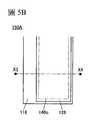
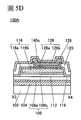
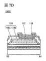
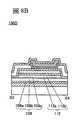
本發明的一個方式是一種包括電晶體及電容元件的半導體裝置,其中電晶體包括:氧化物半導體膜;氧化物半導體膜上的閘極絕緣膜;閘極絕緣膜上的閘極電極;閘極電極上的第二絕緣膜;第二絕緣膜上的第三絕緣膜;第三絕緣膜上的源極電極;以及第三絕緣膜上的汲極電極,源極電極與氧化物半導體膜電連接,汲極電極與氧化物半導體膜電連接,電容元件包括:第一導電膜;第二導電膜;以及第二絕緣膜,第一導電膜與閘極電極設置在同一表面上,第二導電膜與源極電極及汲極電極設置在同一表面上,第二絕緣膜設置在第一導電膜與第二導電膜之間。詳細的內容參照下面。An embodiment of the present invention is a semiconductor device including a transistor and a capacitor element, wherein the transistor includes: an oxide semiconductor film; a gate insulating film on the oxide semiconductor film; a gate electrode on the gate insulating film; a gate electrode A second insulating film on the electrode; a third insulating film on the second insulating film; a source electrode on the third insulating film; and a drain electrode on the third insulating film, the source electrode is electrically connected to the oxide semiconductor film , The drain electrode is electrically connected to the oxide semiconductor film, the capacitor element includes: a first conductive film; a second conductive film; and a second insulating film, the first conductive film and the gate electrode are disposed on the same surface, the second conductive film The source electrode and the drain electrode are provided on the same surface, and the second insulating film is provided between the first conductive film and the second conductive film. For details, refer to the following.
本發明的一個方式是一種包括電晶體及電容元件的半導體裝置,其中電晶體包括:第一絕緣膜上的氧化物半導體膜;氧化物半導體膜上的閘極絕緣膜;閘極絕緣膜上的閘極電極;閘極電極上的第二絕緣膜;第二絕緣膜上的第三絕緣膜;第三絕緣膜上的源極電極;以及第三絕緣膜上的汲極電極,第一絕緣膜具有氧,第二絕緣膜具有氮,源極電極與氧化物半導體膜電連接,汲極電極與氧化物半導體膜電連接,電容元件包括:第一導電膜;第二導電膜;以及第二絕緣膜,第一導電膜與閘極電極設置在同一表面上,第二導電膜與源極電極及汲極電極設置在同一表面上,第二絕緣膜設置在第一導電膜與第二導電膜之間。An embodiment of the present invention is a semiconductor device including a transistor and a capacitor element, wherein the transistor includes: an oxide semiconductor film on the first insulating film; a gate insulating film on the oxide semiconductor film; and a gate insulating film Gate electrode; second insulating film on gate electrode; third insulating film on second insulating film; source electrode on third insulating film; and drain electrode on third insulating film, first insulating film It has oxygen, the second insulating film has nitrogen, the source electrode is electrically connected to the oxide semiconductor film, the drain electrode is electrically connected to the oxide semiconductor film, and the capacitor element includes: a first conductive film; a second conductive film; and a second insulation Film, the first conductive film is provided on the same surface as the gate electrode, the second conductive film is provided on the same surface as the source electrode and the drain electrode, and the second insulating film is provided between the first conductive film and the second conductive film between.
另外,本發明的其他一個方式是一種包括電 晶體及電容元件的半導體裝置,其中電晶體包括:第一絕緣膜上的第一閘極電極;第一閘極電極上的第一閘極絕緣膜;第一閘極絕緣膜上的氧化物半導體膜;氧化物半導體膜上的第二閘極絕緣膜;第二閘極絕緣膜上的第二閘極電極;第二閘極電極上的第二絕緣膜;第二絕緣膜上的第三絕緣膜;第三絕緣膜上的源極電極;以及第三絕緣膜上的汲極電極,第一閘極絕緣膜具有氧,第二絕緣膜具有氮,源極電極與氧化物半導體膜電連接,汲極電極與氧化物半導體膜電連接,電容元件包括:第一導電膜;第二導電膜;以及第二絕緣膜,第一導電膜與第二閘極電極設置在同一表面上,第二導電膜與源極電極及汲極電極設置在同一表面上,第二絕緣膜設置在第一導電膜與第二導電膜之間。In addition, another aspect of the present invention is a semiconductor device including a transistor and a capacitor element, wherein the transistor includes: a first gate electrode on the first insulating film; a first gate insulating film on the first gate electrode The oxide semiconductor film on the first gate insulating film; the second gate insulating film on the oxide semiconductor film; the second gate electrode on the second gate insulating film; the second on the second gate electrode Insulating film; third insulating film on the second insulating film; source electrode on the third insulating film; and drain electrode on the third insulating film, the first gate insulating film has oxygen, and the second insulating film has nitrogen , The source electrode is electrically connected to the oxide semiconductor film, the drain electrode is electrically connected to the oxide semiconductor film, the capacitor element includes: a first conductive film; a second conductive film; and a second insulating film, the first conductive film and the second The gate electrode is provided on the same surface, the second conductive film is provided on the same surface as the source electrode and the drain electrode, and the second insulating film is provided between the first conductive film and the second conductive film.
另外,在上述方式中,較佳為如下:氧化物半導體膜包括第一區域及第二區域,第一區域具有與閘極電極重疊的區域,第二區域具有不與閘極電極重疊的區域,第一區域具有雜質元素濃度為第一濃度的部分,第二區域具有雜質元素濃度為第二濃度的部分,第一濃度與第二濃度不同。另外,在上述方式中,較佳為如下:氧化物半導體膜包括第一區域及第二區域,第一區域具有與第二閘極電極重疊的區域,第二區域具有不與第二閘極電極重疊的區域,第一區域具有雜質元素濃度為第一濃度的部分,第二區域具有雜質元素濃度為第二濃度的部分,第一濃度與第二濃度不同。In addition, in the above aspect, it is preferable that the oxide semiconductor film includes a first region and a second region, the first region has a region overlapping the gate electrode, and the second region has a region not overlapping the gate electrode, The first region has a portion where the impurity element concentration is the first concentration, and the second region has a portion where the impurity element concentration is the second concentration, and the first concentration is different from the second concentration. In addition, in the above aspect, it is preferable that the oxide semiconductor film includes a first region and a second region, the first region has a region overlapping with the second gate electrode, and the second region has a region that does not overlap with the second gate electrode In the overlapping regions, the first region has a portion with an impurity element concentration at a first concentration, and the second region has a portion with an impurity element concentration at a second concentration, and the first concentration is different from the second concentration.
另外,在上述方式中,雜質元素較佳為具有氫、硼、碳、氮、氟、鋁、矽、磷、氯以及稀有氣體元素中的一個以上。另外,在上述方式中,雜質元素較佳為具有氬及氫。In addition, in the above aspect, the impurity element preferably has one or more of hydrogen, boron, carbon, nitrogen, fluorine, aluminum, silicon, phosphorus, chlorine, and a rare gas element. In addition, in the above aspect, the impurity element preferably has argon and hydrogen.
另外,在上述方式中,第二區域較佳為具有接觸於第二絕緣膜的區域。另外,在上述方式中,第二區域較佳為具有雜質元素濃度比第一區域高的區域。另外,在上述方式中,第一區域較佳為具有結晶性比第二區域高的區域。In addition, in the above-described aspect, the second region preferably has a region in contact with the second insulating film. In addition, in the above aspect, the second region preferably has a higher impurity element concentration than the first region. In addition, in the above aspect, the first region preferably has a higher crystallinity than the second region.
另外,在上述方式中,氧化物半導體膜較佳為具有氧、In、Zn及M(M為Ti、Ga、Y、Zr、La、Ce、Nd或Hf)。另外,在上述方式中,氧化物半導體膜較佳為包括結晶部,結晶部較佳為具有c軸配向性及c軸平行於氧化物半導體膜的被形成面的法線向量的部分。In addition, in the above aspect, the oxide semiconductor film preferably has oxygen, In, Zn, and M (M is Ti, Ga, Y, Zr, La, Ce, Nd, or Hf). In the above aspect, the oxide semiconductor film preferably includes a crystal portion, and the crystal portion preferably has a c-axis alignment and a c-axis parallel to the normal vector of the surface of the oxide semiconductor film to be formed.
另外,本發明的其他一個方式是一種包括上述方式中的任一所記載的半導體裝置及顯示元件的顯示裝置。另外,本發明的其他一個方式是一種包括該顯示裝置及觸控感測器的顯示模組。另外,本發明的其他一個方式是一種電子裝置,它包括:上述方式中的任一所記載的半導體裝置、上述顯示裝置或上述顯示模組;以及操作鍵或電池。In addition, another aspect of the present invention is a display device including the semiconductor device and the display element described in any of the above aspects. In addition, another aspect of the present invention is a display module including the display device and the touch sensor. In addition, another aspect of the present invention is an electronic device including: the semiconductor device described in any of the above aspects, the display device, or the display module; and an operation key or a battery.
藉由本發明的一個方式,可以提供一種包括使用氧化物半導體的電晶體的新穎半導體裝置。尤其是,藉由本發明的一個方式,可以提供一種包括使用氧化物半 導體的交錯型電晶體的半導體裝置。此外,可以提供一種半導體裝置,其中包括使用氧化物半導體的交錯型電晶體及連接於該電晶體的電容元件。此外,可以提供一種半導體裝置,其中包括使用氧化物半導體且通態電流大的電晶體。此外,可以提供一種半導體裝置,其中包括使用氧化物半導體且關態電流小的電晶體。此外,可以提供一種半導體裝置,其中包括使用氧化物半導體且佔有面積小的電晶體。本發明的一個方式的其他目的之一是提供一種半導體裝置,其中包括使用氧化物半導體且具有穩定的電特性的電晶體。此外,可以提供一種半導體裝置,其中包括使用氧化物半導體且可靠性高的電晶體。此外,可以提供一種新穎半導體裝置。此外,可以提供一種新穎顯示裝置。According to one aspect of the present invention, a novel semiconductor device including a transistor using an oxide semiconductor can be provided. In particular, according to one aspect of the present invention, a semiconductor device including an interlaced transistor using an oxide semiconductor can be provided. In addition, it is possible to provide a semiconductor device including a staggered transistor using an oxide semiconductor and a capacitor element connected to the transistor. In addition, it is possible to provide a semiconductor device including an transistor using an oxide semiconductor and having a large on-state current. In addition, it is possible to provide a semiconductor device including an transistor using an oxide semiconductor and having a small off-state current. In addition, it is possible to provide a semiconductor device including an transistor using an oxide semiconductor and having a small occupied area. One of the other objects of one aspect of the present invention is to provide a semiconductor device including a transistor using an oxide semiconductor and having stable electrical characteristics. In addition, it is possible to provide a semiconductor device including a transistor that uses an oxide semiconductor and has high reliability. In addition, a novel semiconductor device can be provided. In addition, a novel display device can be provided.
注意,這些效果的記載不妨礙其他效果的存在。此外,本發明的一個方式並不需要具有所有上述效果。另外,從說明書、圖式、申請專利範圍等的記載看來除這些效果外的效果是顯然的,從而可以從說明書、圖式、申請專利範圍等的記載中抽出除這些效果外的效果。Note that the description of these effects does not prevent the existence of other effects. In addition, one aspect of the present invention does not need to have all the above effects. In addition, the effects other than these effects are obvious from the descriptions in the description, drawings, patent application scope, etc., and the effects other than these effects can be extracted from the descriptions in the description, drawings, patent application scope, etc.
100‧‧‧電晶體100‧‧‧Transistor
100A‧‧‧電晶體100A‧‧‧transistor
100B‧‧‧電晶體100B‧‧‧Transistor
100C‧‧‧電晶體100C‧‧‧Transistor
100D‧‧‧電晶體100D‧‧‧transistor
100E‧‧‧電晶體100E‧‧‧transistor
100F‧‧‧電晶體100F‧‧‧Transistor
100G‧‧‧電晶體100G‧‧‧transistor
100H‧‧‧電晶體100H‧‧‧Transistor
102‧‧‧基板102‧‧‧ substrate
104‧‧‧絕緣膜104‧‧‧Insulation film
106‧‧‧導電膜106‧‧‧conductive film
106a‧‧‧導電膜106a‧‧‧conductive film
106b‧‧‧導電膜106b‧‧‧conductive film
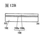
108‧‧‧絕緣膜108‧‧‧Insulation film
108a‧‧‧絕緣膜108a‧‧‧Insulation film
108b‧‧‧絕緣膜108b‧‧‧Insulation film
108c‧‧‧絕緣膜108c‧‧‧Insulation film
110‧‧‧氧化物半導體膜110‧‧‧oxide semiconductor film
110_1‧‧‧氧化物半導體膜110_1‧‧‧oxide semiconductor film
110_2‧‧‧氧化物半導體膜110_2‧‧‧oxide semiconductor film
110a‧‧‧通道區域110a‧‧‧channel area
110a_1‧‧‧通道區域110a_1‧‧‧channel area
110a_2‧‧‧通道區域110a_2‧‧‧channel area
110b‧‧‧低電阻區域110b‧‧‧Low resistance area
110b_1‧‧‧低電阻區域110b_1‧‧‧Low resistance area
110b_2‧‧‧低電阻區域110b_2‧‧‧Low resistance area
110c‧‧‧低電阻區域110c‧‧‧Low resistance area
110c_1‧‧‧低電阻區域110c_1‧‧‧Low resistance area
110c_2‧‧‧低電阻區域110c_2‧‧‧Low resistance area
110d‧‧‧低電阻區域110d‧‧‧Low resistance area
110e‧‧‧低電阻區域110e‧‧‧Low resistance area
110f‧‧‧區域110f‧‧‧Region
110g‧‧‧區域110g‧‧‧region
110h‧‧‧低電阻區域110h‧‧‧Low resistance area
110i‧‧‧低電阻區域110i‧‧‧Low resistance area
112‧‧‧絕緣膜112‧‧‧Insulating film
112a‧‧‧絕緣膜112a‧‧‧Insulation film
112b‧‧‧絕緣膜112b‧‧‧Insulating film
113‧‧‧導電膜113‧‧‧ conductive film
113a‧‧‧導電膜113a‧‧‧conductive film
113b‧‧‧導電膜113b‧‧‧conductive film
114‧‧‧導電膜114‧‧‧conductive film
114a‧‧‧導電膜114a‧‧‧conductive film
114b‧‧‧導電膜114b‧‧‧conductive film
116‧‧‧導電膜116‧‧‧conductive film
116a‧‧‧導電膜116a‧‧‧conductive film
116b‧‧‧導電膜116b‧‧‧conductive film
117‧‧‧絕緣膜117‧‧‧Insulation film
118‧‧‧絕緣膜118‧‧‧Insulation film
120‧‧‧絕緣膜120‧‧‧Insulating film
121‧‧‧導電膜121‧‧‧conductive film
121a‧‧‧導電膜121a‧‧‧conductive film
121b‧‧‧導電膜121b‧‧‧conductive film
122‧‧‧導電膜122‧‧‧conductive film
122a‧‧‧導電膜122a‧‧‧conductive film
122b‧‧‧導電膜122b‧‧‧conductive film
124‧‧‧導電膜124‧‧‧conductive film
124a‧‧‧導電膜124a‧‧‧conductive film
124b‧‧‧導電膜124b‧‧‧conductive film
126‧‧‧導電膜126‧‧‧ conductive film
126a‧‧‧導電膜126a‧‧‧conductive film
126b‧‧‧導電膜126b‧‧‧conductive film
128‧‧‧絕緣膜128‧‧‧Insulation film
139‧‧‧開口部139‧‧‧ opening
140a‧‧‧開口部140a‧‧‧ opening
140b‧‧‧開口部140b‧‧‧ opening
140c‧‧‧開口部140c‧‧‧ opening
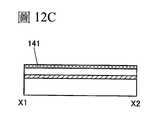
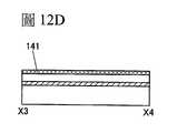
141‧‧‧膜141‧‧‧ film
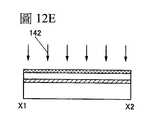
142‧‧‧氧142‧‧‧Oxygen
143‧‧‧雜質元素143‧‧‧ Impurity elements
145‧‧‧遮罩145‧‧‧Mask
150‧‧‧電容元件150‧‧‧capacitor element
150A‧‧‧電容元件150A‧‧‧capacitor element
150B‧‧‧電容元件150B‧‧‧capacitor element
150C‧‧‧電容元件150C‧‧‧capacitor element
150D‧‧‧電容元件150D‧‧‧capacitor element
150E‧‧‧電容元件150E‧‧‧capacitor element
150F‧‧‧電容元件150F‧‧‧capacitor element
150G‧‧‧電容元件150G‧‧‧capacitor element
210‧‧‧電子槍室210‧‧‧Electronic gun room
212‧‧‧光學系統212‧‧‧Optical system
214‧‧‧樣本室214‧‧‧Sample room
216‧‧‧光學系統216‧‧‧Optical system
218‧‧‧照相裝置218‧‧‧Camera installation
220‧‧‧觀察室220‧‧‧ Observation room
222‧‧‧膠片室222‧‧‧ Film room
224‧‧‧電子224‧‧‧Electronics
228‧‧‧物質228‧‧‧Material
232‧‧‧螢光板232‧‧‧ fluorescent board
306‧‧‧導電膜306‧‧‧ conductive film
306a‧‧‧導電膜306a‧‧‧conductive film
306b‧‧‧導電膜306b‧‧‧conductive film
314‧‧‧導電膜314‧‧‧ conductive film
314a‧‧‧導電膜314a‧‧‧conductive film
314b‧‧‧導電膜314b‧‧‧conductive film
316‧‧‧導電膜316‧‧‧ conductive film
316a‧‧‧導電膜316a‧‧‧conductive film
316b‧‧‧導電膜316b‧‧‧conductive film
318‧‧‧導電膜318‧‧‧ conductive film
318a‧‧‧導電膜318a‧‧‧conductive film
318b‧‧‧導電膜318b‧‧‧conductive film
324‧‧‧導電膜324‧‧‧ conductive film
324a‧‧‧導電膜324a‧‧‧conductive film
324b‧‧‧導電膜324b‧‧‧conductive film
326‧‧‧導電膜326‧‧‧ conductive film
326a‧‧‧導電膜326a‧‧‧conductive film
326b‧‧‧導電膜326b‧‧‧conductive film
328‧‧‧導電膜328‧‧‧ conductive film
328a‧‧‧導電膜328a‧‧‧conductive film
328b‧‧‧導電膜328b‧‧‧conductive film
334‧‧‧導電膜334‧‧‧conductive film
334a‧‧‧導電膜334a‧‧‧conductive film
334b‧‧‧導電膜334b‧‧‧conductive film
338‧‧‧導電膜338‧‧‧ conductive film
338a‧‧‧導電膜338a‧‧‧conductive film
338b‧‧‧導電膜338b‧‧‧conductive film
352‧‧‧開口部352‧‧‧Opening
353‧‧‧開口部353‧‧‧Opening
354‧‧‧開口部354‧‧‧Opening
355‧‧‧開口部355‧‧‧ opening
500‧‧‧FET500‧‧‧FET
501‧‧‧基板501‧‧‧ substrate
502‧‧‧基板502‧‧‧ substrate
504B‧‧‧發光元件504B‧‧‧Lighting element
504G‧‧‧發光元件504G‧‧‧Lighting element
504R‧‧‧發光元件504R‧‧‧Lighting element
504W‧‧‧發光元件504W‧‧‧Lighting element
506‧‧‧導電膜506‧‧‧conductive film
507‧‧‧導電膜507‧‧‧ conductive film
508‧‧‧分隔壁508‧‧‧Partition wall
509‧‧‧結構體509‧‧‧Structure
510‧‧‧EL層510‧‧‧EL layer
512‧‧‧導電膜512‧‧‧ conductive film
514B‧‧‧彩色層514B‧‧‧Color layer
514G‧‧‧彩色層514G‧‧‧Color layer
514R‧‧‧彩色層514R‧‧‧Color layer
514W‧‧‧彩色層514W‧‧‧Color layer
516‧‧‧基板516‧‧‧ substrate
518‧‧‧密封膜518‧‧‧Sealing film
520‧‧‧區域520‧‧‧Region
522‧‧‧絕緣膜522‧‧‧Insulation film
524‧‧‧開口部524‧‧‧Opening
700‧‧‧顯示裝置700‧‧‧Display device
701‧‧‧基板701‧‧‧ substrate
702‧‧‧像素部702‧‧‧Pixel Department
704‧‧‧源極驅動電路部704‧‧‧ Source drive circuit
705‧‧‧基板705‧‧‧ substrate
706‧‧‧閘極驅動電路部706‧‧‧ Gate drive circuit
708‧‧‧FPC端子部708‧‧‧FPC terminal
710‧‧‧信號線710‧‧‧Signal cable
711‧‧‧佈線部711‧‧‧Wiring Department
712‧‧‧密封材料712‧‧‧Sealing material
716‧‧‧FPC716‧‧‧FPC
730‧‧‧絕緣膜730‧‧‧Insulation film
732‧‧‧密封膜732‧‧‧Seal film
734‧‧‧絕緣膜734‧‧‧Insulating film
736‧‧‧彩色膜736‧‧‧Color film
738‧‧‧遮光膜738‧‧‧shading film
750‧‧‧電晶體750‧‧‧Transistor
752‧‧‧電晶體752‧‧‧Transistor
760‧‧‧連接電極760‧‧‧Electrode
766‧‧‧絕緣膜766‧‧‧Insulating film
770‧‧‧平坦化絕緣膜770‧‧‧flat insulating film
772‧‧‧導電膜772‧‧‧conductive film
774‧‧‧導電膜774‧‧‧ conductive film
775‧‧‧液晶元件775‧‧‧Liquid crystal element
776‧‧‧液晶層776‧‧‧Liquid crystal layer
778‧‧‧結構體778‧‧‧Structure
780‧‧‧異方性導電膜780‧‧‧Anisotropic conductive film
782‧‧‧發光元件782‧‧‧Lighting element
784‧‧‧導電膜784‧‧‧ conductive film
786‧‧‧EL層786‧‧‧EL layer
788‧‧‧導電膜788‧‧‧ conductive film
790‧‧‧電容元件790‧‧‧capacitor element
1100‧‧‧顆粒1100‧‧‧ particles
1100a‧‧‧顆粒1100a‧‧‧Particles
1100b‧‧‧顆粒1100b‧‧‧Particle
1101‧‧‧顆粒1101‧‧‧Particles
1120‧‧‧基板1120‧‧‧ substrate
1130‧‧‧靶材1130‧‧‧Target
5000‧‧‧基板5000‧‧‧ substrate
5001‧‧‧像素部5001‧‧‧Pixel Department
5002‧‧‧掃描線驅動電路5002‧‧‧scan line drive circuit
5003‧‧‧掃描線驅動電路5003‧‧‧scan line drive circuit
5004‧‧‧信號線驅動電路5004‧‧‧Signal line driver circuit
5010‧‧‧電容佈線5010‧‧‧Capacitor wiring
5012‧‧‧閘極佈線5012‧‧‧Gate wiring
5013‧‧‧閘極佈線5013‧‧‧Gate wiring
5014‧‧‧汲極電極5014‧‧‧Drain electrode
5016‧‧‧電晶體5016‧‧‧transistor
5017‧‧‧電晶體5017‧‧‧transistor
5018‧‧‧液晶元件5018‧‧‧Liquid crystal element
5019‧‧‧液晶元件5019‧‧‧Liquid crystal element
5020‧‧‧像素5020‧‧‧ pixels
5021‧‧‧開關電晶體5021‧‧‧Switch transistor
5022‧‧‧驅動電晶體5022‧‧‧Drive transistor
5023‧‧‧電容元件5023‧‧‧capacitor element
5023a‧‧‧電容元件5023a‧‧‧capacitor element
5023b‧‧‧電容元件5023b‧‧‧capacitor element
5024‧‧‧發光元件5024‧‧‧Lighting element
5025‧‧‧信號線5025‧‧‧Signal cable
5026‧‧‧掃描線5026‧‧‧scan line
5027‧‧‧電源線5027‧‧‧Power cord
5028‧‧‧共用電極5028‧‧‧Common electrode
5111‧‧‧像素5111‧‧‧ pixels
5154‧‧‧發光元件5154‧‧‧Lighting element
5155‧‧‧電晶體5155‧‧‧Transistor
5156‧‧‧電晶體5156‧‧‧Transistor
5157‧‧‧電晶體5157‧‧‧transistor
5158‧‧‧電容元件5158‧‧‧capacitor element
5211‧‧‧像素5211‧‧‧ pixels
5214‧‧‧發光元件5214‧‧‧Lighting element
5215‧‧‧電晶體5215‧‧‧Transistor
5216‧‧‧電晶體5216‧‧‧Transistor
5217‧‧‧電晶體5217‧‧‧transistor
5218‧‧‧電容元件5218‧‧‧capacitor element
5219‧‧‧電晶體5219‧‧‧Transistor
5311‧‧‧像素5311‧‧‧ pixels
5314‧‧‧發光元件5314‧‧‧Lighting element
5315‧‧‧電晶體5315‧‧‧Transistor
5316‧‧‧電晶體5316‧‧‧Transistor
5317‧‧‧電晶體5317‧‧‧Transistor
5318‧‧‧電容元件5318‧‧‧capacitor element
5319‧‧‧電晶體5319‧‧‧Transistor
5320‧‧‧電晶體5320‧‧‧transistor
5411‧‧‧像素5411‧‧‧ pixels
5414‧‧‧發光元件5414‧‧‧Lighting element
5415‧‧‧電晶體5415‧‧‧Transistor
5416‧‧‧電晶體5416‧‧‧Transistor
5417‧‧‧電晶體5417‧‧‧transistor
5418‧‧‧電容元件5418‧‧‧Capacitive element
5440‧‧‧電晶體5440‧‧‧Transistor
5441‧‧‧電晶體5441‧‧‧Transistor
5442‧‧‧電晶體5442‧‧‧Transistor
8000‧‧‧顯示模組8000‧‧‧Display module
8001‧‧‧上蓋8001‧‧‧Top cover
8002‧‧‧下蓋8002‧‧‧ Lower cover
8003‧‧‧FPC8003‧‧‧FPC
8004‧‧‧觸控面板8004‧‧‧Touch panel
8005‧‧‧FPC8005‧‧‧FPC
8006‧‧‧顯示面板8006‧‧‧Display panel
8007‧‧‧背光單元8007‧‧‧Backlight unit
8008‧‧‧光源8008‧‧‧Light source
8009‧‧‧框架8009‧‧‧Frame
8010‧‧‧印刷電路板8010‧‧‧ printed circuit board
8011‧‧‧電池8011‧‧‧Battery
9000‧‧‧外殼9000‧‧‧Housing
9001‧‧‧顯示部9001‧‧‧ Display Department
9002‧‧‧顯示部9002‧‧‧Display
9003‧‧‧揚聲器9003‧‧‧speaker
9004‧‧‧LED燈9004‧‧‧LED light
9005‧‧‧操作鍵9005‧‧‧Operation keys
9006‧‧‧連接端子9006‧‧‧Connecting terminal
9007‧‧‧感測器9007‧‧‧Sensor
9008‧‧‧麥克風9008‧‧‧Microphone
9009‧‧‧開關9009‧‧‧switch
9010‧‧‧紅外線埠9010‧‧‧Infrared port
9011‧‧‧儲存介質讀取部9011‧‧‧Storage Media Reading Department
9012‧‧‧支撐部9012‧‧‧Support
9013‧‧‧耳機9013‧‧‧Headphone
9014‧‧‧天線9014‧‧‧ Antenna
9015‧‧‧快門按鈕9015‧‧‧Shutter button
9016‧‧‧影像接收部9016‧‧‧Image receiving department
9017‧‧‧充電器9017‧‧‧ Charger
在圖式中:In the diagram:
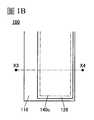
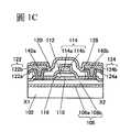
圖1A至1D是示出半導體裝置的一個方式的俯視圖及剖面圖;1A to 1D are a plan view and a cross-sectional view showing one mode of a semiconductor device;
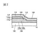
圖2是示出半導體裝置的一個方式的剖面圖;2 is a cross-sectional view showing one embodiment of the semiconductor device;
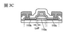
圖3A至3D是示出半導體裝置的一個方式的剖面圖;3A to 3D are cross-sectional views showing one mode of the semiconductor device;
圖4A和4B是示出半導體裝置的一個方式的剖面圖;4A and 4B are cross-sectional views showing one mode of a semiconductor device;
圖5A至5D是示出半導體裝置的一個方式的俯視圖及剖面圖;5A to 5D are a plan view and a cross-sectional view showing one mode of a semiconductor device;
圖6是示出半導體裝置的一個方式的剖面圖;6 is a cross-sectional view showing one embodiment of the semiconductor device;
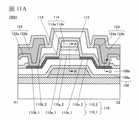
圖7A至7D是示出半導體裝置的一個方式的剖面圖;7A to 7D are cross-sectional views showing one mode of the semiconductor device;
圖8A至8D是示出半導體裝置的一個方式的剖面圖;8A to 8D are cross-sectional views showing one mode of the semiconductor device;
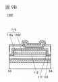
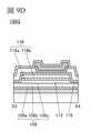
圖9A至9D是示出半導體裝置的一個方式的剖面圖;9A to 9D are cross-sectional views showing one mode of the semiconductor device;
圖10是示出半導體裝置的一個方式的剖面圖;10 is a cross-sectional view showing one embodiment of the semiconductor device;
圖11A至11C是示出半導體裝置的一個方式的剖面圖以及示出能帶圖的一個方式的圖;11A to 11C are cross-sectional views showing one mode of the semiconductor device and diagrams showing one mode of the energy band diagram;
圖12A至12H是示出半導體裝置的製程的一個例子的剖面圖;12A to 12H are cross-sectional views showing an example of the manufacturing process of the semiconductor device;
圖13A至13F是示出半導體裝置的製程的一個例子的剖面圖;13A to 13F are cross-sectional views showing an example of the manufacturing process of the semiconductor device;
圖14A至14F是示出半導體裝置的製程的一個例子的剖面圖;14A to 14F are cross-sectional views showing an example of a manufacturing process of a semiconductor device;
圖15A至15F是示出半導體裝置的製程的一個例子的剖面圖;15A to 15F are cross-sectional views showing an example of the manufacturing process of the semiconductor device;
圖16A至16F是示出半導體裝置的製程的一個例子的剖面圖;16A to 16F are cross-sectional views showing an example of the manufacturing process of the semiconductor device;
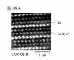
圖17A至17C是氧化物半導體的剖面TEM影像及局部性的傅立葉變換影像;17A to 17C are cross-sectional TEM images of oxide semiconductors and local Fourier transform images;
圖18A至18D是示出氧化物半導體膜的奈米束電子繞射圖案的圖以及透過電子繞射測量裝置的一個例子的圖;18A to 18D are diagrams showing a nanobeam electron diffraction pattern of an oxide semiconductor film and an example of a transmission electron diffraction measurement device;
圖19A至19C是示出利用透過電子繞射測量的結構分析的一個例子的圖以及平面TEM影像;19A to 19C are diagrams showing an example of structural analysis using transmission electron diffraction measurement and planar TEM images;
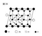
圖20是說明計算模型的圖;20 is a diagram illustrating a calculation model;
圖21A和21B是說明初始狀態及最終狀態的圖;21A and 21B are diagrams illustrating the initial state and the final state;
圖22是說明活化能的圖;22 is a diagram illustrating activation energy;
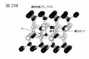
圖23A和23B是說明初始狀態及最終狀態的圖;23A and 23B are diagrams illustrating the initial state and the final state;
圖24是說明活化能的圖;24 is a diagram illustrating activation energy;
圖25是說明VOH的遷移能階的圖;FIG. 25 is a diagram illustrating the migration energy level of VO H;
圖26是示出顯示裝置的一個方式的俯視圖;26 is a plan view showing one mode of the display device;
圖27是示出顯示裝置的一個方式的剖面圖;27 is a cross-sectional view showing one mode of the display device;
圖28是示出顯示裝置的一個方式的剖面圖;28 is a cross-sectional view showing one mode of the display device;
圖29A和29B是說明發光裝置的像素部的結構的圖;29A and 29B are diagrams illustrating the structure of a pixel portion of a light-emitting device;
圖30A至30D是半導體裝置的剖面圖;30A to 30D are cross-sectional views of semiconductor devices;
圖31A至31C是顯示裝置的俯視圖及電路圖;31A to 31C are a top view and a circuit diagram of a display device;
圖32A和32B是顯示裝置的電路圖及時序圖;32A and 32B are circuit diagrams and timing diagrams of the display device;
圖33A和33B是顯示裝置的電路圖及時序圖;33A and 33B are circuit diagrams and timing diagrams of the display device;
圖34A和34B是顯示裝置的電路圖及時序圖;34A and 34B are circuit diagrams and timing diagrams of the display device;
圖35A和35B是顯示裝置的電路圖及時序圖;35A and 35B are circuit diagrams and timing diagrams of the display device;
圖36是說明顯示模組的圖;36 is a diagram illustrating a display module;
圖37A至37H是說明電子裝置的圖;37A to 37H are diagrams illustrating electronic devices;
圖38A和38B是實施例中的剖面TEM影像;38A and 38B are cross-sectional TEM images in the embodiment;
圖39是說明電阻率的溫度依賴性的圖;FIG. 39 is a diagram illustrating the temperature dependence of resistivity;
圖40A至40C是說明CAAC-OS的成膜模型的示意圖、顆粒及CAAC-OS的剖面圖;40A to 40C are schematic diagrams illustrating the film forming model of CAAC-OS, cross-sectional views of particles and CAAC-OS;
圖41是說明nc-OS的成膜模型的示意圖,其中示出顆粒;FIG. 41 is a schematic diagram illustrating a film forming model of nc-OS, in which particles are shown;
圖42是說明顆粒的圖;Figure 42 is a diagram illustrating particles;
圖43是說明在被形成面上施加到顆粒的力量的圖;43 is a diagram illustrating the force applied to the particles on the surface to be formed;
圖44A和44B是說明被形成面上的顆粒的舉動的圖;44A and 44B are diagrams illustrating the behavior of particles on the formed surface;
圖45A和45B是說明InGaZnO4的結晶的圖;45A and 45B are diagrams illustrating the crystallization of InGaZnO4 ;
圖46A和46B是示出原子碰撞之前的InGaZnO4的結構等的圖;46A and 46B are diagrams showing the structure and the like of InGaZnO4 before atomic collision;
圖47A和47B是示出原子碰撞之後的InGaZnO4的結構等的圖;47A and 47B are diagrams showing the structure and the like of InGaZnO4 after atomic collision;
圖48A和48B是示出原子碰撞之後的原子的軌跡的圖;48A and 48B are diagrams showing the trajectories of atoms after collision of atoms;
圖49A和49B是CAAC-OS膜以及靶材的剖面HAADF-STEM影像。49A and 49B are cross-sectional HAADF-STEM images of the CAAC-OS film and target material.
下面,參照圖式對實施方式進行說明。但是,所屬技術領域的普通技術人員可以很容易地理解一個事實,就是實施方式可以以多個不同形式來實施,其方式和詳細內容可以在不脫離本發明的精神及其範圍的條件下被變換為各種各樣的形式。因此,本發明不應該被解釋為僅限定在下面的實施方式所記載的內容中。The embodiment will be described below with reference to the drawings. However, one of ordinary skill in the art can easily understand the fact that the embodiment can be implemented in many different forms, and the manner and details can be changed without departing from the spirit and scope of the present invention For various forms. Therefore, the present invention should not be interpreted as being limited to the contents described in the following embodiments.
在圖式中,為便於清楚地說明,有時誇大表示大小、層的厚度或區域。因此,本發明並不一定限定於上述尺寸。此外,在圖式中,示意性地示出理想的例子,因此本發明不侷限於圖式所示的形狀或數值等。In the drawings, the size, thickness, or area of the layer are sometimes exaggerated for clarity. Therefore, the present invention is not necessarily limited to the above dimensions. In addition, in the drawings, ideal examples are schematically shown, so the present invention is not limited to the shapes, numerical values, etc. shown in the drawings.
本說明書所使用的“第一”、“第二”、“第三”等序數詞是為了避免構成要素的混淆而附加的,而不是為了在數目方面上進行限定的。The ordinal numbers such as "first", "second", and "third" used in this specification are added to avoid confusion of constituent elements, and are not intended to be limited in number.
在本說明書中,為了方便起見,使用“上”“下”等表示配置的詞句以參照圖式說明構成要素的位置關係。另外,構成要素的位置關係根據描述各構成要素的方向適當地改變。因此,不侷限於本說明書中所說明的詞句,根據情況可以適當地更換。In this specification, for convenience, words such as “upper”, “lower”, and the like are used to explain the positional relationship of the constituent elements with reference to the drawings. In addition, the positional relationship of the constituent elements is appropriately changed according to the direction in which each constituent element is described. Therefore, it is not limited to the words and sentences described in this specification, and can be appropriately replaced according to circumstances.
在本說明書等中,電晶體是指至少包括閘極電極、汲極以及源極這三個端子的元件。電晶體在汲極(汲極端子、汲極區域或汲極電極)與源極(源極端子、源極區域或源極電極)之間具有通道區域,並且電流能夠流過汲極、通道區域以及源極。注意,在本說明書等中, 通道區域是指電流主要流過的區域。In this specification and the like, the transistor refers to an element including at least three terminals of a gate electrode, a drain electrode, and a source electrode. The transistor has a channel region between the drain (drain terminal, drain region, or drain electrode) and the source (source terminal, source region, or source electrode), and current can flow through the drain, channel region And the source. Note that in this specification and the like, the channel area refers to an area where current mainly flows.
在使用極性不同的電晶體的情況或電路工作中的電流方向變化的情況等下,“源極”及“汲極”的功能有時互相調換。因此,在本說明書中,“源極”和“汲極”可以互相調換。When using transistors with different polarities or when the direction of the current changes during circuit operation, the functions of "source" and "drain" are sometimes interchanged. Therefore, in this specification, "source" and "drain" can be interchanged.
另外,在本說明書等中,“電連接”包括藉由“具有某種電作用的元件”連接的情況。在此,“具有某種電作用的元件”只要可以進行連接目標間的電信號的授受,就對其沒有特別的限制。例如,“具有某種電作用的元件”不僅包括電極和佈線,而且還包括電晶體等的切換元件、電阻元件、電感器、電容器、其他具有各種功能的元件等。In addition, in this specification and the like, “electrically connected” includes a case of being connected by “an element having a certain electric action”. Here, the “element having a certain electrical function” is not particularly limited as long as it can transmit and receive electrical signals between connected targets. For example, "elements with a certain electrical action" include not only electrodes and wiring, but also switching elements such as transistors, resistance elements, inductors, capacitors, and other elements with various functions.
在本實施方式中,參照圖1A至圖16F說明將電晶體及電容元件設置在同一基板上的半導體裝置以及該半導體裝置的製造方法的一個例子。In this embodiment, an example of a semiconductor device in which a transistor and a capacitor element are provided on the same substrate and a method of manufacturing the semiconductor device will be described with reference to FIGS. 1A to 16F.
圖1A至1D示出將電晶體及電容元件設置在同一基板上的半導體裝置的一個例子。注意,該電晶體採用頂閘極結構。1A to 1D show an example of a semiconductor device in which a transistor and a capacitor element are provided on the same substrate. Note that this transistor uses a top gate structure.
圖1A是半導體裝置所具有的電晶體100的俯視圖,圖1B是半導體裝置所具有的電容元件150的俯視 圖,圖1C是沿著圖1A的點劃線X1-X2的剖面圖,圖1D是沿著圖1B的點劃線X3-X4的剖面圖。注意,為了方便起見,在圖1A及1B中省略基板102、絕緣膜104、絕緣膜108、絕緣膜118、絕緣膜120等。還注意,在後面的電晶體及電容元件的俯視圖中也有時與圖1A及1B同樣地省略構成要素的一部分。此外,有時將點劃線X1-X2的方向稱為通道長度方向,而將點劃線Y1-Y2的方向稱為通道寬度方向。1A is a top view of a
圖1A及1C所示的電晶體100包括:形成在基板102上的絕緣膜108;絕緣膜108上的氧化物半導體膜110;氧化物半導體膜110上的絕緣膜112;隔著絕緣膜112與氧化物半導體膜110重疊的導電膜114;覆蓋氧化物半導體膜110、絕緣膜112及導電膜114的絕緣膜118;絕緣膜118上的絕緣膜120;藉由設置在絕緣膜118及絕緣膜120中的開口部140a連接於氧化物半導體膜110的導電膜122;以及藉由設置在絕緣膜118及絕緣膜120中的開口部140b連接於氧化物半導體膜110的導電膜124。此外,也可以在電晶體100上設置覆蓋絕緣膜120、導電膜122及導電膜124的絕緣膜128。The
在圖1C中,絕緣膜108具有絕緣膜108a及絕緣膜108a上的絕緣膜108b的疊層結構。導電膜114具有導電膜114a及導電膜114a上的導電膜114b的疊層結構。導電膜122具有導電膜122a及導電膜122a上的導電膜122b的疊層結構。導電膜124具有導電膜124a及導電 膜124a上的導電膜124b的疊層結構。In FIG. 1C, the insulating
在電晶體100中,導電膜114具有閘極電極(也稱為頂閘極電極)的功能,導電膜122具有源極電極和汲極電極中之一的功能,導電膜124具有源極電極和汲極電極中之另一的功能。另外,在電晶體100中,絕緣膜108具有氧化物半導體膜110的基底膜的功能,絕緣膜112具有閘極絕緣膜的功能。In the
此外,圖1B及1D所示的電容元件150包括:形成在基板102上的絕緣膜108:絕緣膜108上的絕緣膜112;絕緣膜112上的導電膜116;覆蓋絕緣膜108、絕緣膜112及導電膜116的絕緣膜118;絕緣膜118上的絕緣膜120;以及在設置於絕緣膜120中的開口部140c中隔著絕緣膜118與導電膜116重疊的導電膜126。此外,也可以在電容元件150上設置覆蓋絕緣膜120及導電膜126的絕緣膜128。In addition, the
在圖1D中,絕緣膜108具有絕緣膜108a及絕緣膜108a上的絕緣膜108b的疊層結構。導電膜116具有導電膜116a及導電膜116a上的導電膜116b的疊層結構。導電膜126具有導電膜126a及導電膜126a上的導電膜126b的疊層結構。In FIG. 1D, the insulating
電容元件150是在一對電極之間夾持電介質的結構。更詳細地說,一對電極中之一個是導電膜116,一對電極中之另一個是導電膜126,在導電膜116與導電膜126之間的絕緣膜118被用作電介質。The
用作電晶體100的閘極電極的導電膜114及用作電容元件150的一對電極中之一個的導電膜116藉由相同製程形成,它們的至少一部分形成在同一表面上。用作電晶體100的源極電極及汲極電極的導電膜122及導電膜124以及用作電容元件150的一對電極中之另一個的導電膜126藉由相同製程形成,導電膜122、124和126的至少一部分形成在同一表面上。The
如此,藉由以相同製程形成用作電晶體100及電容元件150的各電極的導電膜,可以減少製造成本。In this way, by forming the conductive films used as the electrodes of the
另外,在電容元件150中,絕緣膜120具有開口部140c。由此,在絕緣膜118和絕緣膜120層疊的絕緣膜中可以只使絕緣膜118用作電介質。藉由採用上述結構,可以增大電容元件150的容量值。由此,可以增大顯示裝置的容量值。In addition, in the
接著,圖2示出沿著圖1A所示的電晶體100的點劃線Y1-Y2(通道寬度方向)的剖面圖。Next, FIG. 2 shows a cross-sectional view along the chain line Y1-Y2 (channel width direction) of the
如圖2所示,在通道寬度方向上導電膜114a的端部位於導電膜114b的端部的外側。絕緣膜112的端部位於導電膜114a的端部的外側。絕緣膜108b在不與絕緣膜112重疊的區域中具有凹部。藉由採用上述結構,可以提高絕緣膜118、絕緣膜120及絕緣膜128的覆蓋性。As shown in FIG. 2, the end of the
接著,下面詳細地說明電晶體100所具有的氧化物半導體膜110。Next, the
在電晶體100的氧化物半導體膜110中,不 與導電膜114重疊的區域包含形成氧缺損的元素。下面,將形成氧缺損的元素稱為雜質元素進行說明。作為雜質元素的典型例子,有氫、硼、碳、氮、氟、鋁、矽、磷、氯以及稀有氣體元素等。作為稀有氣體元素的典型例子,有氦、氖、氬、氪以及氙等。In the
當將雜質元素添加到氧化物半導體膜時,氧化物半導體膜中的金屬元素與氧的鍵合被切斷,以形成氧缺損。或者,當將雜質元素添加到氧化物半導體膜時,鍵合於氧化物半導體膜中的金屬元素的氧與雜質元素鍵合,氧從金屬元素脫離,由此形成氧缺損。其結果是,氧化物半導體膜的載子密度變高,由此導電性變高。When an impurity element is added to the oxide semiconductor film, the bond between the metal element in the oxide semiconductor film and oxygen is cut to form an oxygen defect. Alternatively, when an impurity element is added to the oxide semiconductor film, oxygen bonded to the metal element in the oxide semiconductor film is bonded to the impurity element, and oxygen is detached from the metal element, thereby forming an oxygen defect. As a result, the carrier density of the oxide semiconductor film becomes higher, and thus the conductivity becomes higher.
當對添加了雜質元素形成有氧缺損的氧化物半導體添加氫時,氫進入氧缺損處而在導帶附近形成施體能階。其結果是,氧化物半導體的導電性增高,而成為導電體。可以將成為導電體的氧化物半導體稱為氧化物導電體。一般而言,由於氧化物半導體的能隙大,所以對可見光具有透光性。另一方面,氧化物導電體是在導帶附近具有施體能階的氧化物半導體。因此,起因於該施體能階的吸收的影響小,而對可見光具有與氧化物半導體相同程度的透光性。When hydrogen is added to an oxide semiconductor to which an oxygen element is added to form an oxygen defect, hydrogen enters the oxygen defect and forms a donor level near the conduction band. As a result, the conductivity of the oxide semiconductor is increased to become a conductor. An oxide semiconductor that becomes a conductor can be called an oxide conductor. In general, since the energy gap of an oxide semiconductor is large, it has transparency to visible light. On the other hand, the oxide conductor is an oxide semiconductor having a donor level near the conduction band. Therefore, the absorption due to the donor level has a small effect, and has the same degree of light transmittance as the oxide semiconductor for visible light.
在此,關於使用氧化物導電體形成的膜(以下稱為氧化物導電體膜),參照圖39說明其電阻率的溫度依存性。Here, regarding a film formed using an oxide conductor (hereinafter referred to as an oxide conductor film), the temperature dependence of the resistivity will be described with reference to FIG. 39.
在此,製造具有氧化物導電體膜的樣本。作 為氧化物導電體膜,製造如下氧化物導電體膜:氧化物半導體膜與氮化矽膜接觸而成的氧化物導電體膜(OC_SiNx);在摻雜裝置中將氬添加到氧化物半導體膜且與氮化矽膜接觸而成的氧化物導電體膜(OC_Ar dope+SiNx);在電漿處理裝置中使氧化物半導體膜暴露於氬電漿且與氮化矽膜接觸而形成的氧化物導電體膜(OC_Ar plasma+SiNx)。另外,氮化矽膜包含氫。Here, a sample with an oxide conductor film is manufactured. As the oxide conductor film, the following oxide conductor film is manufactured: an oxide conductor film (OC_SiNx ) in which an oxide semiconductor film is in contact with a silicon nitride film; argon is added to the oxide semiconductor in a doping device Oxide conductor film (OC_Ar dope+SiNx ) formed by the film and contact with the silicon nitride film; formed by exposing the oxide semiconductor film to the argon plasma and contacting the silicon nitride film in the plasma processing device Oxide conductor film (OC_Ar plasma+SiNx ). In addition, the silicon nitride film contains hydrogen.
下面說明包含氧化物導電體膜(OC_SiNx)的樣本的製造方法。在藉由電漿CVD法將400nm厚的氧氮化矽膜形成在玻璃基板上之後,將氧氮化矽膜暴露於氧電漿,然後對氧氮化矽膜添加氧離子,來形成由於加熱而釋放氧的氧氮化矽膜。接著,藉由使用原子個數比為In:Ga:Zn=1:1:1.2的濺射靶材的濺射法在由於加熱而釋放氧的氧氮化矽膜上形成100nm厚的In-Ga-Zn氧化物膜,在450℃的氮氛圍下對該氧化物膜進行加熱處理,然後在450℃的氮及氧的混合氣體氛圍下進行加熱處理。然後,藉由電漿CVD法形成100nm厚的氮化矽膜。然後,在350℃的氮及氧的混合氣體氛圍下進行加熱處理。Next, a method for manufacturing a sample containing an oxide conductor film (OC_SiNx ) will be described. After forming a 400 nm thick silicon oxynitride film on the glass substrate by plasma CVD method, the silicon oxynitride film is exposed to the oxygen plasma, and then oxygen ions are added to the silicon oxynitride film to form due to heating The silicon oxynitride film that releases oxygen. Next, a 100-nm-thick In-Ga was formed on the silicon oxynitride film that released oxygen by heating by a sputtering method using a sputtering target with an atomic ratio of In:Ga:Zn=1:1:1:1.2 -A Zn oxide film, which is heat-treated in a nitrogen atmosphere at 450°C, and then heat-treated in a mixed gas atmosphere of nitrogen and oxygen at 450°C. Then, a 100-nm-thick silicon nitride film is formed by the plasma CVD method. Then, heat treatment is performed in a mixed gas atmosphere of nitrogen and oxygen at 350°C.
下面說明包含氧化物導電體膜(OC_Ar dope+SiNx)的樣本的製造方法。在藉由電漿CVD法將400nm厚的氧氮化矽膜形成在玻璃基板上之後,將氧氮化矽膜暴露於氧電漿,然後對氧氮化矽膜添加氧離子,來形成由於加熱而釋放氧的氧氮化矽膜。接著,藉由使用原子個數比為In:Ga:Zn=1:1:1.2的濺射靶材的濺射法在由於加 熱而釋放氧的氧氮化矽膜上形成100nm厚的In-Ga-Zn氧化物膜,在450℃的氮氛圍下對該氧化物膜進行加熱處理,然後在450℃的氮及氧的混合氣體氛圍下進行加熱處理。接著,利用摻雜裝置以10kV的加速電壓對In-Ga-Zn氧化物膜添加劑量為5×10¹⁴ions/cm2的氬,來在In-Ga-Zn氧化物膜中形成氧缺損。然後,藉由電漿CVD法形成100nm厚的氮化矽膜。然後,在350℃的氮及氧的混合氣體氛圍下進行加熱處理。Next, a method of manufacturing a sample containing an oxide conductor film (OC_Ar dope+SiNx ) will be described. After forming a 400 nm thick silicon oxynitride film on the glass substrate by plasma CVD method, the silicon oxynitride film is exposed to the oxygen plasma, and then oxygen ions are added to the silicon oxynitride film to form due to heating The silicon oxynitride film that releases oxygen. Next, a 100-nm-thick In-Ga was formed on the silicon oxynitride film that released oxygen by heating by a sputtering method using a sputtering target with an atomic ratio of In:Ga:Zn=1:1:1:1.2 -A Zn oxide film, which is heat-treated in a nitrogen atmosphere at 450°C, and then heat-treated in a mixed gas atmosphere of nitrogen and oxygen at 450°C. Next, argon at a dose of 5×10¹⁴ ions/cm2 was added to the In-Ga-Zn oxide film with an acceleration voltage of 10 kV using a doping device to form an oxygen defect in the In-Ga-Zn oxide film. Then, a 100-nm-thick silicon nitride film is formed by the plasma CVD method. Then, heat treatment is performed in a mixed gas atmosphere of nitrogen and oxygen at 350°C.
下面說明包含氧化物導電體膜(OC_Ar plasma+SiNx)的樣本的製造方法。在藉由電漿CVD法將400nm厚的氧氮化矽膜形成在玻璃基板上之後,將氧氮化矽膜暴露於氧電漿,來形成由於加熱而釋放氧的氧氮化矽膜。接著,藉由使用原子個數比為In:Ga:Zn=1:1:1.2的濺射靶材的濺射法在由於加熱而釋放氧的氧氮化矽膜上形成100nm厚的In-Ga-Zn氧化物膜,在450℃的氮氛圍下對該氧化物膜進行加熱處理,然後在450℃的氮及氧的混合氣體氛圍下進行加熱處理。接著,在電漿處理裝置中產生氬電漿,使加速了的氬離子碰撞到In-Ga-Zn氧化物膜,來形成氧缺損。然後,藉由電漿CVD法形成100nm厚的氮化矽膜。然後,在350℃的氮及氧的混合氣體氛圍下進行加熱處理。Next, a method of manufacturing a sample containing an oxide conductor film (OC_Ar plasma+SiNx ) will be described. After a 400-nm-thick silicon oxynitride film was formed on the glass substrate by the plasma CVD method, the silicon oxynitride film was exposed to an oxygen plasma to form a silicon oxynitride film that released oxygen due to heating. Next, a 100-nm-thick In-Ga was formed on the silicon oxynitride film that released oxygen by heating by a sputtering method using a sputtering target with an atomic ratio of In:Ga:Zn=1:1:1:1.2 -A Zn oxide film, which is heat-treated in a nitrogen atmosphere at 450°C, and then heat-treated in a mixed gas atmosphere of nitrogen and oxygen at 450°C. Next, argon plasma is generated in the plasma processing apparatus, and accelerated argon ions collide with the In-Ga-Zn oxide film to form an oxygen defect. Then, a 100-nm-thick silicon nitride film is formed by the plasma CVD method. Then, heat treatment is performed in a mixed gas atmosphere of nitrogen and oxygen at 350°C.
圖39示出測定各樣本的電阻率的結果。在此,利用四端子的范德堡法(van-der-Pauw法)測定電阻率。在圖39中,橫軸表示測定溫度,縱軸表示電阻率。 另外,四角形示出氧化物導電體膜(OC_SiNx)的測定結果,圓圈示出氧化物導電體膜(OC_Ar dope+SiNx)的測定結果,三角形示出氧化物半導體膜(OC_Ar plasma+SiNx)的測定結果。FIG. 39 shows the results of measuring the resistivity of each sample. Here, the resistivity was measured by the four-terminal van der Pauw method (van-der-Pauw method). In FIG. 39, the horizontal axis represents the measured temperature, and the vertical axis represents the resistivity. In addition, the square shows the measurement result of the oxide conductor film (OC_SiNx ), the circle shows the measurement result of the oxide conductor film (OC_Ar dope+SiNx ), and the triangle shows the oxide semiconductor film (OC_Ar plasma+SiNx ) Measurement results.
注意,在圖式中未圖示,但是不與氮化矽膜接觸的氧化物半導體膜的電阻率高,很難測定出其電阻率。由此可知,氧化物導電體膜的電阻率比氧化物半導體膜低。Note that although not shown in the drawings, the oxide semiconductor film that is not in contact with the silicon nitride film has a high resistivity, and it is difficult to measure the resistivity. This shows that the resistivity of the oxide conductor film is lower than that of the oxide semiconductor film.
從圖39可知,當氧化物導電體膜(OC_Ar dope+SiNx)及氧化物導電體膜(OC_Ar plasma+SiNx)包含氧缺損及氫時,電阻率的變動小。典型的是,在80K以上且290K以下的範圍中,電阻率的變動率為小於±20%。或者,在150K以上且250K以下的範圍中,電阻率的變動率為小於±10%。也就是說,氧化物導電體是簡併半導體,可以推測其導帶邊緣與費米能階一致或大致一致。由此,藉由將氧化物導電體膜用作電晶體的源極區域及汲極區域,可以使氧化物導電體膜與用作電晶體的源極電極及汲極電極的導電膜處於歐姆接觸,從而可以在氧化物導電體膜與用作電晶體的源極電極及汲極電極的導電膜之間降低接觸電阻。此外,由於氧化物導電體的電阻率不太依賴於溫度,所以在氧化物導電體膜與用作電晶體的源極電極及汲極電極的導電膜之間接觸電阻的變動量小,由此可以製造可靠性高的電晶體。As can be seen from FIG. 39, when the oxide conductor film (OC_Ar dope+SiNx ) and the oxide conductor film (OC_Ar plasma+SiNx ) contain oxygen defects and hydrogen, the change in resistivity is small. Typically, in the range of 80K or more and 290K or less, the rate of change of resistivity is less than ±20%. Alternatively, in the range of 150K or more and 250K or less, the rate of change of resistivity is less than ±10%. That is to say, the oxide conductor is a degenerate semiconductor, and it can be speculated that its conduction band edge is consistent or roughly consistent with the Fermi energy level. Thus, by using the oxide conductor film as the source region and the drain region of the transistor, the oxide conductor film can be brought into ohmic contact with the conductive film serving as the source electrode and the drain electrode of the transistor Therefore, the contact resistance can be reduced between the oxide conductor film and the conductive films used as the source electrode and the drain electrode of the transistor. In addition, since the resistivity of the oxide conductor is not very temperature-dependent, the amount of change in contact resistance between the oxide conductor film and the conductive film used as the source electrode and the drain electrode of the transistor is small, thereby Transistors with high reliability can be manufactured.
在此,圖3A至3D以及圖4A和4B示出氧化 物半導體膜110附近的放大圖。注意,為了簡化起見,在圖3A至3D以及圖4A和4B中省略構成要素的一部分。Here, FIGS. 3A to 3D and FIGS. 4A and 4B show enlarged views of the vicinity of the
在氧化物半導體膜110的通道長度方向的剖面形狀中,因氧化物半導體膜的載子密度增加而使導電性提高的區域(下面稱為低電阻區域)被形成。如圖3A至3D以及圖4A和4B所示,形成在氧化物半導體膜110中的低電阻區域具有多個構成要素。另外,在圖3A至3D以及圖4A和4B中,通道長度L是夾在一對低電阻區域的區域的長度。In the cross-sectional shape of the
如圖3A所示,氧化物半導體膜110包括:形成在與導電膜114重疊的區域中的通道區域110a;夾著通道區域110a且包含雜質元素的區域,即低電阻區域110b及110c。另外,如圖3A所示,在通道長度方向的剖面形狀中,通道區域110a與低電阻區域110b之間的邊界及通道區域110a與低電阻區域110c之間的邊界隔著絕緣膜112與導電膜114a的下端部一致或者大致一致。就是說,在俯視形狀中,通道區域110a與低電阻區域110b之間的邊界及通道區域110a與低電阻區域110c之間的邊界與導電膜114a的下端部一致或者大致一致。As shown in FIG. 3A, the
如圖3A所示,在通道長度方向的剖面形狀中,也可以導電膜114a的端部位於導電膜114b的端部的外側且導電膜114b具有錐形形狀。就是說,導電膜114a和導電膜114b接觸的面與導電膜114b的側面所成的角度θ1也可以為小於90°、10°以上且85°以下、15°以上且85° 以下、30°以上且85°以下、45°以上且85°以下或60°以上且85°以下。藉由將角度θ1設定為小於90°、10°以上且85°以下、15°以上且85°以下、30°以上且85°以下、45°以上且85°以下或60°以上且85°以下,可以提高導電膜114b的側面上的絕緣膜118的覆蓋性。As shown in FIG. 3A, in the cross-sectional shape in the channel length direction, the end of the
如圖3A所示,在通道長度方向的剖面形狀中,也可以絕緣膜112的端部位於導電膜114a及導電膜114b的端部的外側。另外,絕緣膜112的端部的一部分也可以具有圓弧狀。此外,絕緣膜112也可以具有錐形形狀。就是說,氧化物半導體膜110和絕緣膜112接觸的面與絕緣膜112的側面所成的角度θ2也可以為小於90°,較佳為30°以上且小於90°。As shown in FIG. 3A, in the cross-sectional shape of the channel length direction, the end of the insulating
如圖3B所示,在通道長度方向的剖面形狀中,低電阻區域110b及110c具有隔著絕緣膜112與導電膜114重疊的區域。該區域被用作重疊區域。將通道長度方向上的重疊區域的長度表示為Lov。Lov為通道長度L的小於20%、小於10%、小於5%或小於2%。As shown in FIG. 3B, in the cross-sectional shape of the channel length direction, the low-
如圖3C所示,在通道長度方向的剖面形狀中,通道區域110a具有不與導電膜114a的下端部重疊的區域。該區域被用作偏置區域。將通道長度方向上的偏置區域的長度表示為Loff。注意,在有多個偏置區域的情況下,將一個偏置區域的長度稱為Loff。Loff包含於通道長度L。Loff為通道長度L的小於20%、小於10%、小於5%或小於2%。As shown in FIG. 3C, in the cross-sectional shape in the channel length direction, the
如圖3D所示,在通道長度方向的剖面形狀中,氧化物半導體膜110在通道區域110a與低電阻區域110b之間具有低電阻區域110d,在通道區域110a與低電阻區域110c之間具有低電阻區域110e。低電阻區域110d、110e的雜質元素濃度比低電阻區域110b、110c低且低電阻區域110d、110e的電阻率比低電阻區域110b、110c高。在此,雖然低電阻區域110d、110e與絕緣膜112重疊,但是也可以與絕緣膜112及導電膜114重疊。As shown in FIG. 3D, in the cross-sectional shape of the channel length direction, the
如圖4A所示,在通道長度方向的剖面形狀中,氧化物半導體膜110在與導電膜122、124重疊的區域中具有區域110f、110g。也可以不對區域110f、110g添加雜質元素。此時,氧化物半導體膜110在接觸於導電膜122、124的區域110f、110g與通道區域110a之間包括具有雜質元素的區域,即低電阻區域110b、110c。當對導電膜122、124施加電壓時,區域110f、110g具有導電性,由此區域110f、110g被用作源極區域及汲極區域。As shown in FIG. 4A, in the cross-sectional shape in the channel length direction, the
此外,在形成導電膜122、124之後,將導電膜114、122及124用作遮罩,將雜質元素經過絕緣膜120及絕緣膜118添加到氧化物半導體膜110,來形成圖4A所示的結構。In addition, after the
如圖4B所示,在通道長度方向的剖面形狀中,也可以設置夾著通道區域110a的低電阻區域110b、110c、110d、110e、110h及110i。As shown in FIG. 4B, in the cross-sectional shape of the channel length direction,
明確地說,圖4B所示的氧化物半導體膜110包括:通道區域110a;夾著通道區域110a的低電阻區域110h、110i;夾著低電阻區域110h、110i的低電阻區域110d、110e;夾著低電阻區域110d、110e的低電阻區域110b、110c。經過不與導電膜114b重疊的區域的導電膜114a及絕緣膜112添加雜質元素,來形成低電阻區域110h、110i。經過不與導電膜114a及導電膜114b重疊的區域的絕緣膜112添加雜質元素,來形成低電阻區域110d、110e。藉由直接添加雜質元素形成低電阻區域110b、110c。由此,低電阻區域110h、110i的雜質元素濃度比低電阻區域110d、110e及低電阻區域110b、110c低,且低電阻區域110h、110i的電阻率比低電阻區域110d、110e及低電阻區域110b、110c高。另外,低電阻區域110d、110e的雜質元素濃度比低電阻區域110b、110c低,且低電阻區域110d、110e的電阻率比低電阻區域110b、110c高。Specifically, the
在圖4B中,通道區域110a與導電膜114b重疊。低電阻區域110h、110i與向導電膜114b的外側突出的導電膜114a重疊。低電阻區域110d、110e與向導電膜114a的外側突出的絕緣膜112重疊。低電阻區域110b、110c向絕緣膜112的外側突出且與絕緣膜118重疊。In FIG. 4B, the
如圖3D及圖4B所示,藉由氧化物半導體膜110包括雜質元素濃度比低電阻區域110b、110c低且電阻率比低電阻區域110b、110c高的低電阻區域110d、 110e、110h以及110i,可以使汲極區域的電場緩和。由此,在電晶體中可以減少起因於汲極區域的電場的臨界電壓的變動。As shown in FIGS. 3D and 4B, the
圖3A至3D以及圖4A和4B所示的氧化物半導體膜110包括如下區域:不與絕緣膜112及導電膜114重疊的區域的膜厚度比與絕緣膜112及導電膜114重疊的區域薄。該薄區域的膜厚度比與絕緣膜112及導電膜114重疊的區域的氧化物半導體膜薄,該薄區域的厚度為0.1nm以上且5nm以下。The
氧化物半導體膜110中的低電阻區域110b、110c被用作源極區域及汲極區域。另外,低電阻區域110b、110c、110d、110e、110h及110i包含雜質元素。The
當雜質元素為稀有氣體元素且藉由濺射法形成氧化物半導體膜110時,通道區域110a以及低電阻區域110b、110c、110d、110e、110h及110i都包含稀有氣體元素。另外,低電阻區域110b、110c的稀有氣體元素濃度比通道區域110a高。低電阻區域110b、110c的稀有氣體元素濃度比低電阻區域110d、110e高。低電阻區域110d、110e的稀有氣體元素濃度比低電阻區域110h、110i高。When the impurity element is a rare gas element and the
這是因為如下兩個原因:當藉由濺射法形成氧化物半導體膜110時,使用稀有氣體作為濺射氣體,由此在氧化物半導體膜110中包含稀有氣體;以及,意圖性地對低電阻區域110b、110c添加稀有氣體,以便在氧化 物半導體膜110中形成氧缺損。在低電阻區域110d、110e、110h及110i中,根據形成在低電阻區域110b、110c、110d、110e、110h及110i上的膜結構及膜厚度,為了形成氧缺損添加的稀有氣體的濃度在上述低電阻區域中都不同。此外,也可以對低電阻區域110b、110c、110d、110e、110h及110i添加與通道區域110a不同的稀有氣體元素。This is because of the following two reasons: when the
當雜質元素為硼、碳、氮、氟、鋁、矽、磷或氯時,低電阻區域110b、110c、110d、110e、110h及110i包含上述雜質元素。由此,低電阻區域110b、110c、110d、110e、110h及110i的雜質元素濃度比通道區域110a高。此外,藉由利用二次離子質譜分析法(SIMS:Secondary Ion Mass Spectrometry)獲得的低電阻區域110b、110c、110d、110e、110h及110i的雜質元素濃度可以為5×10¹⁸atoms/cm3以上且1×1022atoms/cm3以下,1×1019atoms/cm3以上且1×1021atoms/cm3以下,或者5×1019atoms/cm3以上且5×1020atoms/cm3以下。When the impurity element is boron, carbon, nitrogen, fluorine, aluminum, silicon, phosphorus, or chlorine, the low-
當雜質元素為氫時,低電阻區域110b、110c、110d、110e、110h及110i的氫濃度比通道區域110a高。此外,藉由利用二次離子質譜分析法獲得的低電阻區域110b、110c、110d、110e、110h及110i的氫濃度可以為8×10¹⁹atoms/cm3以上,1×1020atoms/cm3以上,或者5×1020atoms/cm3以上。When the impurity element is hydrogen, the hydrogen concentration of the
由於低電阻區域110b、110c、110d、110e、 110h及110i具有雜質元素,所以氧缺損增加並載子密度增加。其結果,低電阻區域110b、110c、110d、110e、110h及110i的導電性得到提高。Since the
雜質元素也可以為氫、硼、碳、氮、氟、鋁、矽、磷和氯中的任一個以上與稀有氣體的組合。此時,在低電阻區域110b、110c、110d、110e、110h及110i中,因稀有氣體而形成的氧缺損和添加了的氫、硼、碳、氮、氟、鋁、矽、磷和氯中的任一個以上相互作用,從而有時低電阻區域110b、110c、110d、110e、110h及110i的導電性更高。The impurity element may be a combination of any one or more of hydrogen, boron, carbon, nitrogen, fluorine, aluminum, silicon, phosphorus, and chlorine with a rare gas. At this time, in the low-
當對添加了雜質元素形成有氧缺損的氧化物半導體添加氫時,氫進入氧缺損處而在導帶附近形成施體能階。其結果是,可以形成氧化物導電體。因此,氧化物導電體具有透光性。注意,這裡將成為導電體的氧化物半導體稱為氧化物導電體。When hydrogen is added to an oxide semiconductor to which an oxygen element is added to form an oxygen defect, hydrogen enters the oxygen defect and forms a donor level near the conduction band. As a result, an oxide conductor can be formed. Therefore, the oxide conductor has translucency. Note that the oxide semiconductor that becomes a conductor is called an oxide conductor here.
氧化物導電體是簡併半導體,可以推測其導帶邊緣與費米能階一致或大致一致。由此,氧化物導電體膜與用作電晶體的源極電極及汲極電極的導電膜處於歐姆接觸,從而可以在氧化物導電體膜與用作電晶體的源極電極及汲極電極的導電膜之間降低接觸電阻。The oxide conductor is a degenerate semiconductor, and it can be speculated that the edge of its conduction band is consistent or roughly the same as the Fermi energy level. Thereby, the oxide conductor film is in ohmic contact with the conductive film used as the source electrode and the drain electrode of the transistor, so that the oxide conductor film and the source electrode and the drain electrode used as the transistor Reduce contact resistance between conductive films.
在本實施方式中所示的電晶體100採用通道區域110a夾在用作源極區域及汲極區域的低電阻區域110b和低電阻區域110c的結構。因此,電晶體100的通態電流大且其電場效移動率高。另外,在電晶體100中, 將導電膜114用作遮罩對氧化物半導體膜110添加雜質元素。就是說,可以自對準地形成低電阻區域。The
電晶體100採用用作閘極電極的導電膜114與用作源極電極及汲極電極的導電膜122、124不重疊的結構。由此,可以降低導電膜114與導電膜122及導電膜124之間的寄生電容。其結果是,當使用大面積基板作為基板102時,可以減少導電膜114與導電膜122及導電膜124之間的信號遲延。The
接著,詳細地說明圖1A至1D所示的半導體裝置的其他結構。Next, other structures of the semiconductor device shown in FIGS. 1A to 1D will be described in detail.
作為基板102,可以使用各種基板,而不侷限於特定的基板。作為該基板的例子,可以舉出半導體基板(例如,單晶基板或矽基板)、SOI(Silicon on Insulator:絕緣層上覆矽)基板、玻璃基板、石英基板、塑膠基板、金屬基板、不鏽鋼基板、包含不鏽鋼箔的基板、鎢基板、包含鎢箔的基板、撓性基板、貼合薄膜、包含纖維狀材料的紙或基材薄膜等。作為玻璃基板的一個例子,可以舉出鋇硼矽酸鹽玻璃、鋁硼矽酸鹽玻璃或鈉鈣玻璃等。作為撓性基板、貼合薄膜及基材薄膜等的例子,可以舉出:以聚對苯二甲酸乙二醇酯(PET)、聚萘二甲酸乙二醇酯(PEN)、聚醚碸(PES)為代表的塑膠;丙烯酸樹脂等合成樹脂等;聚丙烯、聚酯、聚氟化乙烯或聚氯乙烯等;聚醯胺、聚醯亞胺、芳族聚醯胺、環氧、無機蒸鍍薄膜或紙等。尤其是,藉由使用半導體基板、單晶基板或SOI基 板等製造電晶體及電容元件,可以製造特性、尺寸或形狀等的偏差小、電流能力高且尺寸小的電晶體及電容元件。當利用上述電晶體及電容元件構成電路時,可以實現電路的低功耗化或電路的高集成化。As the
另外,作為基板102,也可以使用撓性基板,並且在撓性基板上直接形成電晶體及電容元件。或者,也可以將剝離層設置在基板102與電晶體及電容元件之間。剝離層可以用於如下情況,即在其上製造半導體元件的一部分或全部,然後將該半導體裝置的一部分或全部從基板102分離並轉置到其他基板上。此時,也可以將電晶體及電容元件轉置到耐熱性低的基板或撓性基板上。另外,作為上述剝離層,例如可以使用鎢膜與氧化矽膜的無機膜的疊層結構或基板上形成有聚醯亞胺等有機樹脂膜的結構等。In addition, as the
作為被轉置電晶體及電容元件的基板的例子,除了上述可以設置電晶體及電容元件的基板之外,還可以有紙基板、玻璃紙基板、芳族聚醯胺薄膜基板、聚醯亞胺薄膜基板、石材基板、木材基板、布基板(包括天然纖維(絲、棉、麻)、合成纖維(尼龍、聚氨酯、聚酯)或再生纖維(醋酯纖維、銅氨纖維、人造纖維、再生聚酯)等)、皮革基板、橡膠基板等。藉由使用上述基板,可以形成特性良好的電晶體或功耗低的電晶體,可以製造不容易發生故障並具有耐熱性的裝置,或者可以實現輕量化或薄型化。As examples of the substrate where the transistor and the capacitive element are transposed, in addition to the substrate on which the transistor and the capacitive element can be provided, there can be a paper substrate, a cellophane substrate, an aromatic polyamide film substrate, and a polyimide film Substrates, stone substrates, wood substrates, cloth substrates (including natural fibers (silk, cotton, hemp), synthetic fibers (nylon, polyurethane, polyester) or recycled fibers (acetate fibers, cuprammonium fibers, rayon fibers, recycled polyester ) Etc.), leather substrates, rubber substrates, etc. By using the above substrate, a transistor with good characteristics or a transistor with low power consumption can be formed, a device that is less prone to failure and has heat resistance can be manufactured, or the weight or thickness can be reduced.
藉由適當地利用濺射法、CVD法、蒸鍍法、脈衝雷射沉積(PLD)法、印刷法及塗佈法等,可以形成絕緣膜108。另外,例如可以以單層或疊層使用氧化物絕緣膜或氮化物絕緣膜形成絕緣膜108。此外,為了提高絕緣膜108與氧化物半導體膜110的介面特性,較佳為使用氧化物絕緣膜形成絕緣膜108的至少與氧化物半導體膜110接觸的區域。另外,藉由使用由於加熱而釋放氧的氧化物絕緣膜作為絕緣膜108,可以經過加熱處理而使包含在絕緣膜108中的氧移到氧化物半導體膜110中。The insulating
絕緣膜108的厚度可以為50nm以上、100nm以上且3000nm以下或200nm以上且1000nm以下。藉由增加絕緣膜108的厚度,可以增加絕緣膜108的氧釋放量,而且還可以降低在絕緣膜108和氧化物半導體膜110的介面的介面能階密度以及包含在氧化物半導體膜110的通道區域110a中的氧缺損。The thickness of the insulating
絕緣膜108例如可以使用氧化矽、氧氮化矽、氮氧化矽、氮化矽、氧化鋁、氧化鉿、氧化鎵或者Ga-Zn氧化物等,並且以疊層或單層設置。在本實施方式中,作為絕緣膜108a使用氮化矽膜,作為絕緣膜108b使用氧氮化矽。For the insulating
氧化物半導體膜110典型地使用In-Ga氧化物、In-Zn氧化物、In-M-Zn氧化物(M為Ti、Ga、Y、Zr、La、Ce、Nd或Hf)等金屬氧化物形成。此外,氧化物半導體膜110具有透光性。The
另外,在氧化物半導體膜110為In-M-Zn氧化物的情況下,當In與M之和為100atomic%時,In與M的原子百分比如下:In為25atomic%以上且M低於75atomic%或者In為34atomic%以上且M低於66atomic%。In addition, in the case where the
氧化物半導體膜110的能隙為2eV以上、2.5eV以上或3eV以上。The energy gap of the
氧化物半導體膜110的厚度為3nm以上且200nm以下、3nm以上且100nm以下或3nm以上且60nm以下。The thickness of the
當氧化物半導體膜110為In-M-Zn氧化物時,用來形成In-M-Zn氧化物膜的濺射靶材的金屬元素的原子個數比較佳為滿足In

當氧化物半導體膜110包含第14族元素之一的矽或碳時,氧化物半導體膜110中氧缺損增加,使得氧化物半導體膜110被n型化。因此,在氧化物半導體膜110中,尤其在通道區域110a中,可以將矽或碳的濃度(利用二次離子質譜分析法測得的濃度)設定為2×10¹⁸atoms/cm3以下,或者2×1017atoms/cm3以下。其結果,電晶體具有臨界電壓成為正的電特性(也稱為常關閉特 性)。When the
另外,在氧化物半導體膜110中,尤其在通道區域110a中,可以將利用二次離子質譜分析法測得的鹼金屬或鹼土金屬的濃度設定為1×10¹⁸atoms/cm3以下,或者2×1016atoms/cm3以下。有時當鹼金屬及鹼土金屬與氧化物半導體鍵合時生成載子而使電晶體的關態電流增大。由此,較佳為降低通道區域110a的鹼金屬或鹼土金屬的濃度。其結果,電晶體具有臨界電壓成為正的電特性(也稱為常關閉特性)。In addition, in the
當在氧化物半導體膜110中,尤其在通道區域110a中含有氮時,有時生成作為載子的電子,載子密度增加,使得通道區域110a被n型化。其結果是,使用含有氮的氧化物半導體膜的電晶體容易具有常開啟特性。因此,在該氧化物半導體膜中,尤其在通道區域110a中較佳為儘可能地減少氮,例如,可以將利用二次離子質譜分析法測得的氮濃度設定為5×10¹⁸atoms/cm3以下。When nitrogen is contained in the
藉由在氧化物半導體膜110中,尤其在通道區域110a中降低雜質元素,可以降低氧化物半導體膜的載子密度。在氧化物半導體膜110中,尤其在通道區域110a中,可以將載子密度設定為1×10¹⁷個/cm3以下、1×1015個/cm3以下、1×1013個/cm3以下、1×1011個/cm3以下、或者1×10-9個/cm3以上且1×1010個/cm3以下。By reducing the impurity element in the
藉由作為氧化物半導體膜110使用雜質濃度低且缺陷態密度低的氧化物半導體膜,可以製造具有更優 良的電特性的電晶體。這裡,將雜質濃度低且缺陷態密度低(氧缺損少)的狀態稱為“高純度本質”或“實質上高純度本質”。因為高純度本質或實質上高純度本質的氧化物半導體的載子發生源較少,所以有可能降低載子密度。因此,在該氧化物半導體膜中形成有通道區域的電晶體容易實現正臨界電壓的電特性(也稱為常關閉特性)。因為高純度本質或實質上高純度本質的氧化物半導體膜具有較低的缺陷態密度,所以有可能具有較低的陷阱態密度。高純度本質或實質上高純度本質的氧化物半導體膜的關態電流顯著低,當源極電極與汲極電極間的電壓(汲極電壓)在1V至10V的範圍時,關態電流也可以為半導體參數分析儀的測定極限以下,即1×10-13A以下。因此,在該氧化物半導體膜中形成有通道區域的電晶體的電特性變動小,該電晶體有時成為可靠性高的電晶體。By using an oxide semiconductor film having a low impurity concentration and a low density of defect states as the
氧化物半導體膜110例如可以為非單晶結構。非單晶結構例如包括下述CAAC-OS(C Axis Aligned Crystalline Oxide Semiconductor:c軸配向結晶氧化物半導體)、多晶結構、下述微晶結構或非晶結構。在非單晶結構中,非晶結構的缺陷態密度最高,而CAAC-OS的缺陷態密度最低。The
此外,也可以氧化物半導體膜110為具有非晶結構的區域、微晶結構的區域、多晶結構的區域、CAAC-OS的區域和單晶結構的區域中的兩種以上的區域的混合膜。混合膜有時採用例如具有非晶結構的區域、微 晶結構的區域、多晶結構的區域、CAAC-OS的區域和單晶結構的區域中的兩種以上的區域的單層結構。另外,混合膜有時採用例如層疊有非晶結構的區域、微晶結構的區域、多晶結構的區域、CAAC-OS的區域和單晶結構的區域中的兩種以上的疊層結構。In addition, the
在氧化物半導體膜110中,有時通道區域110a的結晶性與低電阻區域110b、110c、110d、110e、110h及110i不同。具體地,在氧化物半導體膜110中,通道區域110a的結晶性比低電阻區域110b、110c、110d、110e、110h及110i高。這是因為當對低電阻區域110b、110c、110d、110e、110h及110i添加雜質元素時低電阻區域110b、110c、110d、110e、110h及110i會受到損傷而使結晶性降低的緣故。In the
可以以單層或疊層使用氧化物絕緣膜或氮化物絕緣膜形成絕緣膜112。此外,為了提高絕緣膜112與氧化物半導體膜110的介面特性,較佳為使用氧化物絕緣膜形成絕緣膜112的至少與氧化物半導體膜110接觸的區域。絕緣膜112例如可以使用氧化矽、氧氮化矽、氮氧化矽、氮化矽、氧化鋁、氧化鉿、氧化鎵或者Ga-Zn氧化物等,並且以疊層或單層設置。The insulating
另外,藉由作為絕緣膜112設置具有阻擋氧、氫、水等的效果的絕緣膜,能夠防止氧從氧化物半導體膜110擴散到外部,並能夠防止氫、水等從外部侵入氧化物半導體膜110。作為具有阻擋氧、氫、水等的效果的 絕緣膜,可以舉出氧化鋁膜、氧氮化鋁膜、氧化鎵膜、氧氮化鎵膜、氧化釔膜、氧氮化釔膜、氧化鉿膜、氧氮化鉿膜等。In addition, by providing an insulating film having an effect of blocking oxygen, hydrogen, water, etc. as the insulating
此外,藉由作為絕緣膜112使用矽酸鉿(HfSiOx)、添加有氮的矽酸鉿(HfSixOyNz)、添加有氮的鋁酸鉿(HfAlxOyNz)、氧化鉿、氧化釔等high-k材料,能夠降低電晶體的閘極漏電流。In addition, by using hafnium silicate (HfSiOx ), nitrogen-added hafnium silicate (HfSix Oy Nz ), nitrogen-added hafnium aluminate (HfAlx Oy Nz ), and oxidation as the insulating
另外,藉由使用由於加熱而釋放氧的氧化物絕緣膜作為絕緣膜112,可以經過加熱處理而使包含在絕緣膜112中的氧移到氧化物半導體膜110中。In addition, by using an oxide insulating film that releases oxygen due to heating as the insulating
絕緣膜112的厚度例如可以為5nm以上且400nm以下、5nm以上且300nm以下、或者10nm以上且250nm以下。The thickness of the insulating
藉由利用濺射法、真空蒸鍍法、脈衝雷射沉積(PLD)法及熱CVD法等,可以形成導電膜114、導電膜116、導電膜122、導電膜124及導電膜126。導電膜114、導電膜116、導電膜122、導電膜124及導電膜126例如可以使用選自鋁、鉻、銅、鉭、鈦、鉬、鎳、鐵、鈷、鎢中的金屬元素、以上述金屬元素為成分的合金或組合上述金屬元素的合金等形成。另外,還可以使用選自錳和鋯中的一種或多種的金屬元素。導電膜114、導電膜116、導電膜122、導電膜124及導電膜126可以具有單層結構或兩層以上的疊層結構。例如,可以舉出包含矽的鋁膜的單層結構、包含錳的銅膜的單層結構、在鋁膜上層 疊鈦膜的兩層結構、在氮化鈦膜上層疊鈦膜的兩層結構、在氮化鈦膜上層疊鎢膜的兩層結構、在氮化鉭膜或氮化鎢膜上層疊鎢膜的兩層結構、在包含錳的銅膜上層疊銅膜的兩層結構、依次層疊鈦膜、鋁膜及鈦膜的三層結構以及依次層疊包含錳的銅膜、銅膜及包含錳的銅膜的三層結構等。另外,還可以使用組合鋁與選自鈦、鉭、鎢、鉬、鉻、釹、鈧中的元素的一種或多種而形成的合金膜或氮化膜。The
此外,由於同時形成導電膜114及導電膜116,所以它們具有相同材料及相同疊層結構。此外,由於同時形成導電膜122、導電膜124及導電膜126,所以它們具有相同材料及相同疊層結構。In addition, since the
導電膜114、導電膜116、導電膜122、導電膜124及導電膜126也可以使用銦錫氧化物(ITO)、包含氧化鎢的銦氧化物、包含氧化鎢的銦鋅氧化物、包含氧化鈦的銦氧化物、包含氧化鈦的銦錫氧化物、銦鋅氧化物、包含氧化矽的銦錫氧化物等透光導電材料。另外,還可以採用上述透光導電材料與上述金屬元素的疊層結構。For the
導電膜114、導電膜116、導電膜122、導電膜124及導電膜126的厚度例如可以為30nm以上且500nm以下或者100nm以上且400nm以下。The thickness of the
絕緣膜118使用氮化絕緣膜。作為該氮化絕緣膜,可以使用氮化矽、氮氧化矽、氮化鋁、氮氧化鋁等形成。絕緣膜118的氫濃度較佳為1×10²²atoms/cm3以 上。另外,絕緣膜118與氧化物半導體膜110的低電阻區域接觸。由此,由於在氧化物半導體膜110中絕緣膜118所包含的氫擴散到氧化物半導體膜110的低電阻區域中,所以低電阻區域的氫濃度比氧化物半導體膜110的通道區域高。As the insulating
可以以單層或疊層使用氧化物絕緣膜或氮化物絕緣膜形成絕緣膜120。絕緣膜120例如可以使用氧化矽、氧氮化矽、氮氧化矽、氮化矽、氧化鋁、氧化鉿、氧化鎵或者Ga-Zn氧化物等,並且以單層或疊層設置。The insulating
絕緣膜128較佳為具有阻擋來自外部的氫、水等的膜的功能。絕緣膜128例如可以使用氮化矽、氮氧化矽、氧化鋁等,並且以單層或疊層設置。The insulating
絕緣膜118、絕緣膜120及絕緣膜128的厚度分別可以為30nm以上且500nm以下或者100nm以上且400nm以下。The thicknesses of the insulating
接著,參照圖5A至5D及圖6詳細地說明圖1A至1D所示的半導體裝置的其他結構。Next, other structures of the semiconductor device shown in FIGS. 1A to 1D will be described in detail with reference to FIGS. 5A to 5D and FIG. 6.
圖5A是半導體裝置所具有的電晶體100A的俯視圖,圖5B是半導體裝置所具有的電容元件150A的俯視圖,圖5C是沿著圖5A的點劃線X1-X2的剖面圖,圖5D是沿著圖5B的點劃線X3-X4的剖面圖。5A is a plan view of a
圖5A及5C所示的電晶體100A包括:形成 在基板102上的絕緣膜104:絕緣膜104上的導電膜106;絕緣膜104及導電膜106上的絕緣膜108;隔著絕緣膜108與導電膜106重疊的氧化物半導體膜110;氧化物半導體膜110上的絕緣膜112;隔著絕緣膜112與氧化物半導體膜110重疊的導電膜114;覆蓋氧化物半導體膜110、絕緣膜112及導電膜114的絕緣膜118;絕緣膜118上的絕緣膜120;藉由設置在絕緣膜118及絕緣膜120中的開口部140a連接於氧化物半導體膜110的導電膜122;以及藉由設置在絕緣膜118及絕緣膜120中的開口部140b連接於氧化物半導體膜110的導電膜124。此外,也可以在電晶體100A上設置覆蓋絕緣膜120、導電膜122及導電膜124的絕緣膜128。
在圖5C中,導電膜106具有導電膜106a及導電膜106a上的導電膜106b的疊層結構。絕緣膜108具有絕緣膜108a及絕緣膜108a上的絕緣膜108b的疊層結構。導電膜114具有導電膜114a及導電膜114a上的導電膜114b的疊層結構。導電膜122具有導電膜122a及導電膜122a上的導電膜122b的疊層結構。導電膜124具有導電膜124a及導電膜124a上的導電膜124b的疊層結構。In FIG. 5C, the
在電晶體100A中,導電膜106具有第一閘極電極(也稱為底閘極電極)的功能,導電膜114具有第二閘極電極(也稱為頂閘極電極)的功能,導電膜122具有源極電極和汲極電極中之一的功能,導電膜124具有源極電極和汲極電極中之另一的功能。另外,在電晶體100A 中,絕緣膜108具有第一閘極絕緣膜的功能,絕緣膜112具有第二閘極絕緣膜的功能。In the
在圖5A及5C所示的電晶體100A採用在氧化物半導體膜110的上下具有用作閘極電極的導電膜的結構,這是與上面所說明的電晶體100之間不同。如電晶體100A所示,本發明的一個方式的半導體裝置也可以設置兩個以上的閘極電極。The
此外,圖5B及5D所示的電容元件150A包括:形成在基板102上的絕緣膜104;絕緣膜104上的絕緣膜108:絕緣膜108上的絕緣膜112;絕緣膜112上的導電膜116;覆蓋絕緣膜108、絕緣膜112及導電膜116的絕緣膜118;絕緣膜118上的絕緣膜120;以及在設置於絕緣膜120中的開口部140c中隔著絕緣膜118與導電膜116重疊的導電膜126。此外,也可以在電容元件150A上設置覆蓋絕緣膜120及導電膜126的絕緣膜128。In addition, the
在圖5D中,絕緣膜108具有絕緣膜108a及絕緣膜108a上的絕緣膜108b的疊層結構。導電膜116具有導電膜116a及導電膜116a上的導電膜116b的疊層結構。導電膜126具有導電膜126a及導電膜126a上的導電膜126b的疊層結構。In FIG. 5D, the insulating
電容元件150A是在一對電極之間夾持電介質的結構。更詳細地說,一對電極中之一個是導電膜116,一對電極中之另一個是導電膜126,在導電膜116與導電膜126之間的絕緣膜118被用作電介質。The
用作電晶體100A的第二閘極電極的導電膜114及用作電容元件150A的一對電極中之一個的導電膜116藉由相同製程形成,它們的至少一部分形成在同一表面上。用作電晶體100A的源極電極及汲極電極的導電膜122及導電膜124以及用作電容元件150A的一對電極中之另一個的導電膜126藉由相同製程形成,它們的至少一部分形成在同一表面上。The
如此,藉由以同一製程形成用作電晶體100A及電容元件150A的各電極的導電膜,可以減少製造成本。In this way, by forming the conductive films used as the electrodes of the
另外,在電容元件150A中,絕緣膜120具有開口部140c。由此,在絕緣膜118和絕緣膜120層疊的絕緣膜中可以只使絕緣膜118用作電介質。藉由採用上述結構,可以增大電容元件150A的容量值。由此,可以增大顯示裝置的容量值。In addition, in the
接著,圖6示出沿著圖5A所示的電晶體100A的點劃線Y3-Y4(通道寬度方向)的剖面圖。Next, FIG. 6 shows a cross-sectional view along the chain line Y3-Y4 (channel width direction) of the
如圖6所示,用作第二閘極電極的導電膜114在設置於絕緣膜108及絕緣膜112中的開口部139中連接於用作第一閘極電極的導電膜106。由此,導電膜114及導電膜106被供應相同電位。此外,也可以採用不設置開口部139而不使導電膜114與導電膜106連接的結構。當不使導電膜114與導電膜106連接時,導電膜114及導電膜106也可以被供應不同電位。As shown in FIG. 6, the
如圖6所示,氧化物半導體膜110與用作第一閘極電極的導電膜106及用作第二閘極電極的導電膜114對置地設置,夾在用作閘極電極的兩個導電膜。用作第二閘極電極的導電膜114的通道寬度方向的長度比氧化物半導體膜110的通道寬度方向長,通道寬度方向上的整個氧化物半導體膜110隔著絕緣膜112被導電膜114覆蓋。用作第二閘極電極的導電膜114及用作第一閘極電極的導電膜106在絕緣膜108及絕緣膜112中的開口部139中互相連接,由此,氧化物半導體膜110的通道寬度方向的側面中的一個隔著絕緣膜112與用作第二閘極電極的導電膜114對置。As shown in FIG. 6, the
換句話說,在電晶體100A的通道寬度方向上,在用作第一閘極電極的導電膜106及用作第二閘極電極的導電膜114在用作第一閘極絕緣膜的絕緣膜108及用作第二閘極絕緣膜的絕緣膜112中的開口部中互相連接的同時,隔著用作第一閘極絕緣膜的絕緣膜108及用作第二閘極絕緣膜的絕緣膜112包圍氧化物半導體膜110。In other words, in the channel width direction of the
藉由採用上述結構,可以由用作第一閘極電極的導電膜106及用作第二閘極電極的導電膜114的電場電性上包圍電晶體100A所包括的氧化物半導體膜110。如電晶體100A所示,可以將上述電晶體的裝置結構稱為surrounded channel結構(s-channel結構,被包圍通道結構),該s-channel結構為如下:由第一閘極電極及第二閘極電極的電場電性上包圍形成有通道區域的氧化物半導 體膜。By adopting the above-described structure, the
電晶體100A具有s-channel結構。因此,用作第一閘極電極的導電膜106或用作第二閘極電極的導電膜114可以對氧化物半導體膜110高效率地施加用來使電子移動的電場,由此,電晶體100A的電流驅動能力得到提高,從而可以獲得高通態電流特性。另外,因為可以提高通態電流,所以可以使電晶體100A微型化。此外,電晶體100A採用氧化物半導體膜110被用作第一閘極電極的導電膜106及用作第二閘極電極的導電膜114包圍的結構,由此可以提高電晶體100A的機械強度。
在電晶體100A的通道寬度方向上,可以在沒有形成開口部139的氧化物半導體膜110的側面中形成與開口部139不同的開口部。In the channel width direction of the
作為電晶體100A及電容元件150A所具有的絕緣膜104,可以使用與絕緣膜108的材料相同的材料。在此,作為絕緣膜104,藉由利用PECVD設備形成100nm厚的氮化矽膜。As the insulating
作為電晶體100A所具有的導電膜106,可以使用與導電膜114、122、124的材料相同的材料。在此,作為導電膜106a,藉由利用濺射裝置形成10nm厚的氮化鉭膜,作為導電膜106b,藉由利用濺射裝置形成300nm厚的銅膜。As the
接著,參照圖7A至圖11A詳細地說明圖1A至1D以及圖5A至5D所示的半導體裝置的其他結構。注 意,圖7A至圖11A所示的半導體裝置為圖5A至5D所示的半導體裝置的變形例。Next, other structures of the semiconductor device shown in FIGS. 1A to 1D and FIGS. 5A to 5D will be described in detail with reference to FIGS. 7A to 11A. Note that the semiconductor device shown in FIGS. 7A to 11A is a modification of the semiconductor device shown in FIGS. 5A to 5D.
圖7A示出半導體裝置所具有的電晶體100B的剖面圖,圖7B示出半導體裝置所具有的電容元件150B的剖面圖。注意,電晶體100B及電容元件150B的俯視圖分別與圖5A及5B所示的俯視圖相同,在此省略。另外,圖7C所示的電晶體100C、圖7D所示的電容元件150C、圖8A所示的電晶體100D、圖8B所示的電容元件150D、圖8C所示的電晶體100E、圖8D所示的電容元件150E,圖9A所示的電晶體100F、圖9B所示的電容元件150F、圖9C所示的電晶體100G、圖9D所示的電容元件150G的俯視圖也分別與圖5A及5B所示的俯視圖相同,在此省略。7A shows a cross-sectional view of the
另外,在圖7A至圖11A所示的結構中,當具有與上面說明的功能相同的功能時有時使用相同的陰影線,而不特別附加元件符號。In addition, in the structures shown in FIGS. 7A to 11A, when the same functions as those described above are used, the same hatched lines are sometimes used, and no element symbols are particularly added.
圖7A所示的電晶體100B與圖5C所示的電晶體100A的不同之處在於導電膜114的形狀。明確地說,電晶體100B所具有的導電膜114是導電膜114a及導電膜114a上的導電膜114b的疊層結構,其中導電膜114a的下端部與絕緣膜112的上端部一致或大致一致,並且導電膜114b的下端部位於導電膜114a的上端部內側。導電膜 114b的端部的一部分具有圓弧狀。The
圖7B所示的電容元件150B與圖5D所示的電容元件150A的不同之處在於導電膜116的形狀。明確地說,電容元件150B所具有的導電膜116是導電膜116a及導電膜116a上的導電膜116b的疊層結構,其中導電膜116a的下端部與絕緣膜112的上端部一致或大致一致,並且導電膜116b的下端部位於導電膜116a的上端部內側。The
藉由採用圖7A、7B所示的絕緣膜112及/或導電膜114、116的形狀,可以提高絕緣膜118的覆蓋性。By adopting the shapes of the insulating
圖7C所示的電晶體100C與圖5C所示的電晶體100A的不同之處在於絕緣膜112的形狀。明確地說,在電晶體100C所具有的絕緣膜112中,絕緣膜112的下端部及上端部位於導電膜114的下端部的外側。就是說,電晶體100C具有絕緣膜112延伸到導電膜114的外側。藉由採用圖7C所示的絕緣膜112的形狀,可以使氧化物半導體膜110的通道區域和絕緣膜118相隔,從而可以抑制絕緣膜118所包含的氮、氫等進入氧化物半導體膜110的通道區域。The
圖7D所示的電容元件150C與圖5D所示的電容元件150A的不同之處在於絕緣膜112的形狀。明確 地說,在電容元件150C所具有的絕緣膜112中,絕緣膜112的下端部及上端部位於導電膜116的下端部的外側。The
藉由採用圖7C、7D所示的絕緣膜112的形狀,可以提高絕緣膜118的覆蓋性。By adopting the shape of the insulating
圖8A所示的電晶體100D與圖5C所示的電晶體100A的不同之處在於絕緣膜108及絕緣膜112的結構。明確地說,圖8A所示的電晶體100D所具有的絕緣膜108採用絕緣膜108a、絕緣膜108b及絕緣膜108c的疊層結構。另外,圖8A所示的電晶體100D所具有的絕緣膜112採用絕緣膜112a及絕緣膜112b的疊層結構。The
圖8B所示的電容元件150D與圖5D所示的電容元件150A的不同之處在於絕緣膜108及絕緣膜112的結構。明確地說,圖8B所示的電容元件150D所具有的絕緣膜108採用絕緣膜108a、絕緣膜108b及絕緣膜108c的疊層結構。另外,圖8B所示的電容元件150D所具有的絕緣膜112採用絕緣膜112a及絕緣膜112b的疊層結構。The
圖8A及8B所示的絕緣膜108c及絕緣膜112a可以使用氮化氧化物的能階密度低的氧化物絕緣膜而形成。注意,該氮化氧化物的能階密度有時可能會形成在價帶頂的能量(Ev_os)和導帶底的能量(Ec_os)之間。作為在價帶頂的能量(Ev_os)和導帶底的能量 (Ec_os)之間的氮化氧化物的能階密度低的氧化物絕緣膜,可以使用氮氧化物的釋放量少的氧氮化矽膜或氮氧化物的釋放量少的氧氮化鋁膜等。另外,絕緣膜108c及絕緣膜112a的平均膜厚度為0.1nm以上且50nm以下或0.5nm以上且10nm以下。The insulating
此外,在熱脫附譜分析(TDS:Thermal Desorption Spectroscopy)中,氮氧化物的釋放量少的氧氮化矽膜是氨釋放量比氮氧化物的釋放量多的膜,典型的是氨釋放量為1×10¹⁸個/cm3以上且5×1019個/cm3以下。注意,該氨釋放量為在進行膜表面溫度為50℃以上且650℃以下,較佳為50℃以上且550℃以下的加熱處理時的釋放量。In addition, in Thermal Desorption Spectroscopy (TDS: Thermal Desorption Spectroscopy), a silicon oxynitride film with a small amount of nitrogen oxide is a film with more ammonia released than nitrogen oxide, typically ammonia release. The amount is 1×10¹⁸ pieces/cm3 or more and 5×10¹⁹ pieces/cm3 or less. Note that the amount of ammonia released is the amount of release when the heat treatment of the film surface temperature is 50°C or more and 650°C or less, preferably 50°C or more and 550°C or less.
藉由使用由於加熱而釋放氧的氧化物絕緣膜,可以形成絕緣膜108b及絕緣膜112b。另外,絕緣膜108b及絕緣膜112b的平均膜厚度為5nm以上且1000nm以下或10nm以上且500nm以下。By using an oxide insulating film that releases oxygen due to heating, the insulating
作為由於加熱而釋放氧的氧化物絕緣膜的典型例子,有氧氮化矽膜、氧氮化鋁膜等。As typical examples of the oxide insulating film that releases oxygen due to heating, there are a silicon oxynitride film, an aluminum oxynitride film, and the like.
氮氧化物(NOx,x為0以上且2以下,較佳為1以上且2以下),典型的是NO2或NO,在絕緣膜108及絕緣膜112等中形成能階。該能階位於在氧化物半導體膜110的能隙中。由此,當氮氧化物擴散在絕緣膜108與氧化物半導體膜110的介面、絕緣膜112與氧化物半導體膜110的介面以及絕緣膜108與絕緣膜112的介面 中,有時該能階在絕緣膜108、112的一側俘獲電子。其結果,被俘獲的電子留在絕緣膜108、絕緣膜112及氧化物半導體膜110的介面附近,由此使電晶體的臨界電壓向正方向漂移。Nitrogen oxides (NOx , x is 0 or more and 2 or less, preferably 1 or more and 2 or less), typically NO2 or NO, and energy levels are formed in the insulating
另外,當進行加熱處理時,氮氧化物與氨及氧起反應。當進行加熱處理時,絕緣膜108b、112b所包含的氮氧化物與絕緣膜108c、112a所包含的氨起反應,由此絕緣膜108b、112b所包含的氮氧化物減少。因此,在絕緣膜108與氧化物半導體膜110的介面、絕緣膜112與氧化物半導體膜110的介面以及絕緣膜108與絕緣膜112的介面中不容易俘獲電子。In addition, when heat treatment is performed, nitrogen oxide reacts with ammonia and oxygen. When heat treatment is performed, the nitrogen oxide contained in the insulating
藉由使用在價帶頂的能量(Ev_os)和導帶底的能量(Ec_os)之間的氮化氧化物的能階密度低的氧化物絕緣膜作為絕緣膜108c、112a,可以降低電晶體的臨界電壓的漂移,從而可以降低電晶體的電特性的變動。By using an oxide insulating film with a low energy density of the nitride oxide between the energy at the top of the valence band (Ev_os ) and the energy at the bottom of the conduction band (Ec_os ) as the insulating
藉由進行電晶體的製程的加熱處理,典型的是300℃以上且低於基板應變點的加熱處理,絕緣膜108、112在以100K以下的ESR測得的ESR譜中觀察到:g值為2.037以上且2.039以下的第一信號;g值為2.001以上且2.003以下的第二信號;以及g值為1.964以上且1.966以下的第三信號。在X帶的ESR測定中,第一信號與第二信號的分裂寬度及第二信號與第三信號的分裂寬度大約為5mT。另外,g值為2.037以上且2.039以下的第一信號、g值為2.001以上且2.003以下的第二信 號以及g值為1.964以上且1.966以下的第三信號的自旋密度的總和低於1×10¹⁸spins/cm3,典型為1×1017spins/cm3以上且低於1×1018spins/cm3。By performing a heat treatment in the transistor manufacturing process, typically a heat treatment above 300°C and below the strain point of the substrate, the
在100K以下的ESR譜中,g值為2.037以上且2.039以下的第一信號、g值為2.001以上且2.003以下的第二信號以及g值為1.964以上且1.966以下的第三信號相當於起因於氮氧化物(NOx,x為0以上且2以下,較佳為1以上且2以下)的信號。作為氮氧化物的典型例子,有一氧化氮、二氧化氮等。就是說,g值為2.037以上且2.039以下的第一信號、g值為2.001以上且2.003以下的第二信號以及g值為1.964以上且1.966以下的第三信號的自旋密度的總數越少,氧化物絕緣膜中的氮氧化物含量越少。In the ESR spectrum below 100K, a first signal with a g value of 2.037 or more and 2.039 or less, a second signal with a g value of 2.001 or more and 2.003 or less, and a third signal with a g value of 1.964 or more and 1.966 or less correspond to the cause A signal of nitrogen oxides (NOx, x is 0 or more and 2 or less, preferably 1 or more and 2 or less). As typical examples of nitrogen oxides, there are nitric oxide, nitrogen dioxide, and the like. That is, the smaller the total number of spin densities of the first signal having a g value of 2.037 or more and 2.039 or less, the second signal having a g value of 2.001 or more and 2.003 or less, and the third signal having a g value of 1.964 or more and 1.966 or less, The smaller the nitrogen oxide content in the oxide insulating film.
另外,包含氮且缺陷量少的氧化物絕緣膜是藉由利用SIMS測定的氮濃度為6×10²⁰atoms/cm3以下的膜。In addition, the oxide insulating film containing nitrogen and having a small amount of defects is a film having a nitrogen concentration measured by SIMS of 6×10²⁰ atoms/cm3 or less.
藉由利用基板溫度為220℃以上、280℃以上或350℃以上且使用矽烷及一氧化二氮的PECVD法而形成包含氮且缺陷量少的氧化物絕緣膜,來可以形成緻密且硬度高的膜。By using the PECVD method in which the substrate temperature is 220°C or higher, 280°C or higher, or 350°C or higher and using silane and nitrous oxide to form an oxide insulating film containing nitrogen and having a small amount of defects, a dense and high-hardness film can be formed membrane.
圖8C所示的電晶體100E與圖5C所示的電晶體100A的不同之處在於絕緣膜112及導電膜114的形狀。 明確地說,電晶體100E所具有的絕緣膜112的端部的一部分具有圓弧狀。另外,導電膜114a的下端部及上端部位於絕緣膜112的上端部的內側。導電膜114b的下端部位於導電膜114a的上端部的內側。導電膜114a及導電膜114b的端部的一部分具有圓弧狀。The
圖8D所示的電容元件150E與圖5D所示的電容元件150A的不同之處在於絕緣膜112及導電膜116的形狀。明確地說,電容元件150E所具有的絕緣膜112的端部的一部分具有圓弧狀。另外,導電膜116a的下端部及上端部位於絕緣膜112的上端部的內側。導電膜116b的下端部位於導電膜116a的上端部的內側。導電膜116a及導電膜116b的端部的一部分具有圓弧狀。The
圖9A所示的電晶體100F與圖5C所示的電晶體100A的不同之處在於絕緣膜112及導電膜114的形狀等。明確地說,電晶體100F所具有的絕緣膜112及導電膜114在剖面上具有矩形形狀。另外,電晶體100F在氧化物半導體膜110與絕緣膜118之間具有絕緣膜117。The
圖9B所示的電容元件150F與圖5D所示的電容元件150A的不同之處在於絕緣膜112及導電膜116的形狀等。明確地說,電容元件150F所具有的絕緣膜112及導電膜116在剖面上也具有矩形形狀。另外,電容元件150F在導電膜116與絕緣膜118之間具有絕緣膜 117。The
圖9A及9B所示的絕緣膜117可以使用圖8A及8B所示的電晶體100D及電容元件150D所說明的氧化物絕緣膜形成,該氧化物絕緣膜可用於絕緣膜108c、112a且包含氮且缺陷量少。The insulating
當使電晶體100F具有圖9A所示的形狀時,有時形成在氧化物半導體膜110中的低電阻區域的形狀成為圖10所示的結構。When the
圖10是圖9A所示的電晶體100F的氧化物半導體膜110附近的放大圖。如圖10所示,在氧化物半導體膜110的通道長度方向的剖面形狀中,因氧化物半導體膜的載子密度增加而使導電性提高的區域(低電阻區域)被形成。在圖10中,通道長度L為夾在一對低電阻區域的區域的長度。FIG. 10 is an enlarged view of the vicinity of the
在通道長度方向的剖面形狀中,圖10所示的氧化物半導體膜110在通道區域110a與低電阻區域110b之間具有低電阻區域110d,在通道區域110a與低電阻區域110c之間具有低電阻區域110e。低電阻區域110d、110e的雜質元素濃度比低電阻區域110b、110c低且低電阻區域110d、110e的電阻率比低電阻區域110b、110c高。注意,低電阻區域110d、110e與接觸於絕緣膜112及導電膜114的側面的絕緣膜117重疊。在此,低電阻區域110d、110e也可以與絕緣膜112及導電膜114重疊。In the cross-sectional shape in the channel length direction, the
藉由氧化物半導體膜110包括雜質元素濃度 比低電阻區域110b、110c低且電阻率比低電阻區域110b、110c高的低電阻區域110d及110e,可以使汲極區域的電場緩和。由此,在電晶體中可以減少起因於汲極區域的電場的臨界電壓的變動。The
圖9C所示的電晶體100G與圖5C所示的電晶體100A的不同之處在於絕緣膜112及氧化物半導體膜110的形狀。明確地說,電晶體100G所具有的絕緣膜112具有兩個膜厚度,其中一個是與導電膜114重疊的區域的膜厚度,另一個是不與導電膜114重疊的區域的膜厚度。不與導電膜114重疊的區域的膜厚度比與導電膜114重疊的區域薄。此外,絕緣膜112覆蓋氧化物半導體膜110,由此在整個氧化物半導體膜110的部分中膜厚度為大致一致。The transistor 100G shown in FIG. 9C is different from the
圖9D所示的電容元件150G與圖5D所示的電容元件150A的不同之處在於絕緣膜112的形狀。明確地說,電容元件150G所具有的絕緣膜112具有兩個膜厚度,其中一個是與導電膜116重疊的區域的膜厚度,另一個是不與導電膜116重疊的區域的膜厚度。不與導電膜116重疊的區域的膜厚度比與導電膜116重疊的區域薄。The
作為形成圖9C及9D所示的絕緣膜112的形成方法,例如可以舉出如下方法:在對導電膜114進行加工之後,當去除絕緣膜112時留下不與導電膜114重疊的 區域的絕緣膜112。As a method of forming the insulating
在圖9C所示的電晶體100G中,絕緣膜112與氧化物半導體膜110的通道區域110a以及低電阻區域110b、110c接觸。另外,在絕緣膜112中,與低電阻區域110b、110c接觸的區域的膜厚度比與通道區域110a接觸的區域薄,典型的是,絕緣膜112的平均膜厚度為0.1nm以上且50nm以下或0.5nm以上且10nm以下。其結果,可以在隔著絕緣膜112對氧化物半導體膜110添加雜質元素的同時,使絕緣膜118所包含的氫經過絕緣膜112移到氧化物半導體膜110中。因此,可以形成低電阻區域110b、110c。In the transistor 100G shown in FIG. 9C, the insulating
藉由使用包含氮且缺陷量少的氧化物絕緣膜作為絕緣膜112,可以在絕緣膜112中不容易生成氮氧化物,由此可以降低絕緣膜112與氧化物半導體膜110之間的介面中的載子陷阱。其結果,可以降低電晶體的臨界電壓的漂移,從而可以降低電晶體的電特性的變動。By using an oxide insulating film containing nitrogen and having a small amount of defects as the insulating
並且,絕緣膜108採用絕緣膜108a、絕緣膜108b及絕緣膜108c的多層結構,例如使用氮化物絕緣膜形成絕緣膜108a,使用由於加熱而釋放氧的氧氮化矽膜形成絕緣膜108b,使用包含氮且缺陷量少的氧化物絕緣膜形成絕緣膜108c。並且,使用包含氮且缺陷量少的氧化物絕緣膜形成絕緣膜112。就是說,可以使用包含氮且缺陷量少的氧化物絕緣膜覆蓋氧化物半導體膜110。其結果,在經過加熱處理而使絕緣膜108b所包含的氧移到氧 化物半導體膜110中以降低氧化物半導體膜110的通道區域110a所包含的氧缺損的同時,可以降低絕緣膜108c及112與氧化物半導體膜110之間的介面中的載子陷阱。其結果,可以降低電晶體的臨界電壓的漂移,從而可以降低電晶體的電特性的變動。In addition, the insulating
圖11A所示的電晶體100H與圖5C所示的電晶體100A的不同之處在於氧化物半導體膜110的結構。明確地說,電晶體100H所具有的氧化物半導體膜110包括氧化物半導體膜110_1以及接觸於氧化物半導體膜110_1的氧化物半導體膜110_2。就是說,氧化物半導體膜110具有多層結構。The
圖11A所示的電晶體100H的氧化物半導體膜110具有上面說明的低電阻區域。明確地說,電晶體100H的氧化物半導體膜110包括通道區域110a_1、通道區域110a_2、低電阻區域110b_1、低電阻區域110b_2、低電阻區域110c_1以及低電阻區域110c_2。The
在此,圖11B示出包括電晶體100H的通道區域的A-B剖面的能帶圖。此外,氧化物半導體膜110_2的能隙比氧化物半導體膜110_1大。絕緣膜108a、108b及絕緣膜112的能隙比氧化物半導體膜110_1及氧化物半導體膜 110_2大。另外,氧化物半導體膜110_1、氧化物半導體膜110_2、絕緣膜108a、108b及絕緣膜112的費米能階(表示為Ef)位於各本質費米能階(表示為Ei)的位置上。導電膜106及導電膜114的功函數與該費米能階相同。Here, FIG. 11B shows an energy band diagram of the A-B section of the channel region including the
當將閘極電壓設定為電晶體的臨界電壓以上時,由於在氧化物半導體膜110_1與氧化物半導體膜110_2之間的導帶底的能量差,電子優先於氧化物半導體膜110_1流動。就是說,可以估計出電子被埋入氧化物半導體膜110_1。注意,將導帶底的能量表示為Ec,將價帶頂的能量表示為Ev。When the gate voltage is set to be higher than the critical voltage of the transistor, electrons flow preferentially over the oxide semiconductor film 110_1 due to the energy difference between the bottom of the conduction band between the oxide semiconductor film 110_1 and the oxide semiconductor film 110_2. That is, it can be estimated that electrons are buried in the oxide semiconductor film 110_1. Note that the energy at the bottom of the conduction band is expressed as Ec, and the energy at the top of the valence band is expressed as Ev.
由此,在根據本發明的一個方式的電晶體中,藉由埋入電子可以降低介面散射的影響。因此,根據本發明的一個方式的電晶體的通道電阻小。Thus, in the transistor according to an aspect of the present invention, the influence of interface scattering can be reduced by embedding electrons. Therefore, the transistor according to one aspect of the present invention has a small channel resistance.
接著,圖11C示出包括電晶體的源極區域或汲極區域的C-D剖面上的能帶圖。注意,低電阻區域110c_1及低電阻區域110c_2處於簡併狀態。另外,在低電阻區域110c_1中,氧化物半導體膜110_1的費米能階與導帶底的能量相等。在低電阻區域110c_2中,氧化物半導體膜110_2的費米能階與導帶底的能量相等。Next, FIG. 11C shows an energy band diagram on the C-D cross section including the source region or the drain region of the transistor. Note that the low resistance region 110c_1 and the low resistance region 110c_2 are in a degenerate state. In addition, in the low-resistance region 110c_1, the Fermi level of the oxide semiconductor film 110_1 is equal to the energy at the bottom of the conduction band. In the low resistance region 110c_2, the Fermi level of the oxide semiconductor film 110_2 is equal to the energy at the bottom of the conduction band.
此時,在具有源極電極或汲極電極的功能的導電膜124和低電阻區域110c_2之間其能障充分小,所以導電膜124和低電阻區域110c_2處於歐姆接觸。低電阻區域110c_2與低電阻區域110c_1處於歐姆接觸。由此 可知,在導電膜124與氧化物半導體膜110_1及氧化物半導體膜110_2之間電子的授受很順利。At this time, since the energy barrier between the
在具有源極電極和汲極電極中之一的功能的導電膜122與氧化物半導體膜110的低電阻區域110b_1及氧化物半導體膜110的低電阻區域110b_2接觸的區域中也可以進行與圖11C所說明同樣的說明。11C can also be performed in a region where the
如上所述,根據本發明的一個方式的電晶體為在源極電極及汲極電極與通道區域之間電子的授受很順利且通道電阻小的電晶體。即,可知它具有優異的開關特性。As described above, the transistor according to one embodiment of the present invention is a transistor in which the transmission and reception of electrons between the source electrode and the drain electrode and the channel region are smooth and the channel resistance is small. That is, it can be seen that it has excellent switching characteristics.
接著,參照圖30A至30D說明圖5A至5D所示的本發明的一個方式的半導體裝置的各導電膜的連接部及交叉部的結構。圖30A至30C示出各導電膜的連接部的結構的剖面圖,圖30D示出兩個導電膜的交叉部的結構的剖面圖。Next, the structure of the connection portion and the intersection portion of each conductive film of the semiconductor device of one embodiment of the present invention shown in FIGS. 5A to 5D will be described with reference to FIGS. 30A to 30D. 30A to 30C show cross-sectional views of the structure of the connection portion of each conductive film, and FIG. 30D shows a cross-sectional view of the structure of the intersection of two conductive films.
圖30A所示的連接部包括:基板102上的絕緣膜104;絕緣膜104上的導電膜306;覆蓋導電膜306的絕緣膜108;絕緣膜108上的絕緣膜112;設置在絕緣膜112上且在設置於絕緣膜112及絕緣膜108中的開口部352中與導電膜306連接的導電膜314;覆蓋絕緣膜108、112及導電膜314的絕緣膜118;絕緣膜118上的絕緣膜120;設置在絕緣膜120上且在設置於絕緣膜118及 絕緣膜120中的開口部353中與導電膜314連接的導電膜318;以及覆蓋絕緣膜120及導電膜318的絕緣膜128。The connection portion shown in FIG. 30A includes: an insulating
圖30B所示的連接部包括:基板102上的絕緣膜104;絕緣膜104上的絕緣膜108;絕緣膜108上的絕緣膜112;絕緣膜112上的導電膜324;覆蓋絕緣膜108、112及導電膜324的絕緣膜118;絕緣膜118上的絕緣膜120;設置在絕緣膜120上且設置於絕緣膜118及絕緣膜120中的開口部354中與導電膜324連接的導電膜328;以及覆蓋絕緣膜120及導電膜328的絕緣膜128。The connection portion shown in FIG. 30B includes: an insulating
圖30C所示的連接部包括:基板102上的絕緣膜104;絕緣膜104上的導電膜316;覆蓋導電膜316的絕緣膜108;絕緣膜108上的絕緣膜112;設置在絕緣膜112上且在設置於絕緣膜112及絕緣膜108中的開口部355中與導電膜316連接的導電膜334;覆蓋絕緣膜108及導電膜334的絕緣膜118;絕緣膜118上的絕緣膜120;以及絕緣膜120上的絕緣膜128。The connection portion shown in FIG. 30C includes: an insulating
圖30D所示的交叉部包括:基板102上的絕緣膜104;絕緣膜104上的導電膜326;覆蓋導電膜326的絕緣膜108;絕緣膜108上的絕緣膜118;絕緣膜118上的絕緣膜120;絕緣膜120上的導電膜338;以及導電膜338上的絕緣膜128。The intersection shown in FIG. 30D includes: an insulating
在圖30A至30D中,絕緣膜108具有絕緣膜108a及絕緣膜108a上的絕緣膜108b的疊層結構。在圖30A中,導電膜306具有導電膜306a及導電膜306a上的 導電膜306b的疊層結構,導電膜314具有導電膜314a及導電膜314a上的導電膜314b的疊層結構,導電膜318具有導電膜318a及導電膜318a上的導電膜318b的疊層結構。在圖30B中,導電膜324具有導電膜324a及導電膜324a上的導電膜324b的疊層結構,導電膜328具有導電膜328a及導電膜328a上的導電膜328b的疊層結構。在圖30C中,導電膜316具有導電膜316a及導電膜316a上的導電膜316b的疊層結構,導電膜334具有導電膜334a及導電膜334a上的導電膜334b的疊層結構。在圖30D中,導電膜326具有導電膜326a及導電膜326a上的導電膜326b的疊層結構,導電膜338具有導電膜338a及導電膜338a上的導電膜338b的疊層結構。In FIGS. 30A to 30D, the insulating
導電膜306、316、326藉由與電晶體100A所具有的導電膜106相同的製程形成。就是說,導電膜106、306、316、326的至少一部分形成在同一表面上。另外,導電膜314、324、334藉由與電晶體100A所具有的導電膜114及電容元件150A所具有的導電膜116相同的製程形成。就是說,導電膜114、116、314、324、334的至少一部分形成在同一表面上。另外,導電膜318、328、338藉由與電晶體100A所具有的導電膜122及導電膜124以及電容元件150A所具有的導電膜126相同的製程形成。就是說,導電膜124、126、318、328、338的至少一部分形成在同一表面上。The
如圖30D所示,在導電膜326與導電膜338 之間設置有絕緣膜108、118及120。就是說,在導電膜326與導電膜338之間層疊有多個絕緣膜。藉由採用如圖30D所示的導電膜的交叉部的結構,可以在導電膜交叉的部分中降低寄生電容。其結果,可以降低由於寄生電容而產生的信號遲延。As shown in FIG. 30D, insulating
接著,參照圖12A至圖16F說明圖1A至1D所示的電晶體100及電容元件150的製造方法的一個例子。Next, an example of a method of manufacturing the
構成電晶體100及電容元件150的膜(絕緣膜、氧化物半導體膜、導電膜等)可以藉由濺射法、化學氣相沉積(CVD)法、真空蒸鍍法、脈衝雷射沉積(PLD)法形成。或者,可以藉由塗佈法或印刷法形成。作為成膜方法的典型,有濺射法、電漿化學氣相沉積(PECVD)法,但也可以使用熱CVD法。作為熱CVD法的例子,可以使用MOCVD(有機金屬化學氣相沉積)法或ALD(原子層沉積)法。The films (insulating film, oxide semiconductor film, conductive film, etc.) constituting the
藉由熱CVD法進行的沉積可以按以如下方式執行:藉由將處理室內的壓力設定為大氣壓或減壓,將源氣體及氧化劑同時供應到處理室內,並使其在基板附近或基板上相互反應而沉積在基板上。如此,由於熱CVD法不發生電漿來形成膜,因此具有不產生起因於電漿損傷的缺陷的優點。The deposition by the thermal CVD method can be performed as follows: by setting the pressure in the processing chamber to atmospheric pressure or reduced pressure, the source gas and the oxidizing agent are simultaneously supplied into the processing chamber, and are allowed to interact with each other near or on the substrate It is deposited on the substrate by reaction. In this way, since the thermal CVD method does not generate plasma to form a film, there is an advantage that defects due to plasma damage are not generated.
另外,藉由ALD法進行的沉積可以按如下方 式執行:將處理室內的壓力設定為大氣壓或減壓,將用於反應的源氣體依次引入處理室內,然後按該順序反復地引入氣體。例如,藉由切換各自的開關閥(也稱為高速閥)來將兩種以上的源氣體依次供應到處理室內。在該情況下,以防止多種源氣體混合的方式在將第一源氣體引入的同時或之後將惰性氣體(氬或氮等)等引入,然後將第二源氣體引入。注意,在將第一源氣體和惰性氣體同時引入的情況下,惰性氣體用作載子氣體,並且,惰性氣體也可以在將第二源氣體引入的同時引入。另外,也可以不引入惰性氣體而藉由真空抽氣將第一源氣體排出,然後引入第二源氣體。第一源氣體吸附於基板表面上,以形成第一單原子層;然後第二源氣體被引入以與第一單原子層起反應;其結果,第二單原子層層疊於第一單原子層上,從而形成薄膜。In addition, the deposition by the ALD method can be performed as follows: the pressure in the processing chamber is set to atmospheric pressure or reduced pressure, the source gas for the reaction is sequentially introduced into the processing chamber, and then the gas is repeatedly introduced in this order. For example, by switching the respective on-off valves (also called high-speed valves), two or more source gases are sequentially supplied into the processing chamber. In this case, an inert gas (argon, nitrogen, etc.) or the like is introduced at the same time or after the first source gas is introduced in a manner to prevent mixing of multiple source gases, and then the second source gas is introduced. Note that in the case where the first source gas and the inert gas are simultaneously introduced, the inert gas is used as the carrier gas, and the inert gas may also be introduced at the same time as the second source gas is introduced. In addition, the first source gas may be exhausted by vacuum exhaust without introducing an inert gas, and then the second source gas may be introduced. The first source gas is adsorbed on the substrate surface to form a first monoatomic layer; then the second source gas is introduced to react with the first monoatomic layer; as a result, the second monoatomic layer is stacked on the first monoatomic layer To form a thin film.
藉由按該順序反復多次地引入氣體直到獲得所希望的厚度為止,由此可以形成步階覆蓋性良好的薄膜。薄膜的厚度可以根據按該順序反復引入氣體的次數來調整,因此ALD法可以準確地調整厚度,因而適用於製造微型電晶體。By repeatedly introducing the gas in this order multiple times until the desired thickness is obtained, a thin film with good step coverage can be formed. The thickness of the thin film can be adjusted according to the number of times the gas is repeatedly introduced in this order, so the ALD method can accurately adjust the thickness, and thus is suitable for manufacturing micro transistors.
此外,圖12A、12C、12E、12G、圖13A、13C、13E、圖14A、14C、14E、圖15A、15C、15E以及圖16A、16C、16E是說明電晶體100的製造方法的剖面圖,圖12B、12D、12F、12H、圖13B、13D、13F、圖14B、14D、14F、圖15B、15D、15F以及圖16B、16D、 16F是說明電容元件150的製造方法的剖面圖。In addition, FIGS. 12A, 12C, 12E, 12G, FIGS. 13A, 13C, 13E, FIGS. 14A, 14C, 14E, FIGS. 15A, 15C, 15E, and FIGS. 16A, 16C, 16E are cross-sectional views illustrating a method of manufacturing the
首先,在基板102上形成絕緣膜108(絕緣膜108a及108b)(參照圖12A及12B)。First, an insulating film 108 (insulating
藉由適當地利用濺射法、CVD法、蒸鍍法、脈衝雷射沉積(PLD)法、印刷法及塗佈法等,可以形成絕緣膜108。在本實施方式中,作為絕緣膜108a,利用PECVD設備形成100nm厚的氮化矽膜。作為絕緣膜108b,利用PECVD設備形成400nm厚的氧氮化矽膜。The insulating
此外,也可以在形成絕緣膜108b之後,對絕緣膜108b添加氧。作為對絕緣膜108b添加的氧種類,有氧自由基、氧原子、氧原子離子、氧分子離子等。此外,作為添加方法,有離子摻雜法、離子植入法、電漿處理等。另外,也可以在絕緣膜上形成抑制氧的脫離的膜之後,經過該膜對絕緣膜108b添加氧。In addition, after forming the insulating
藉由採用以下述條件,能夠因經過加熱處理而釋放氧的氧化矽膜或氧氮化矽膜形成氧化矽膜或氧氮化矽膜作為絕緣膜108b:在180℃以上且280℃以下或200℃以上且240℃以下的溫度下保持設置在電漿PECVD設備的抽成真空的處理室內的基板,將源氣體導入處理室,將處理室內的壓力設定為100Pa以上且250Pa以下或100Pa以上且200Pa以下,並對設置在處理室內的電極供應0.17W/cm2以上且0.5W/cm2以下或0.25W/cm2以上且0.35W/cm2以下的高頻功率。By adopting the following conditions, a silicon oxide film or a silicon oxynitride film capable of releasing oxygen due to heat treatment to form a silicon oxide film or a silicon oxynitride film as the insulating
在此,說明如下方法:在絕緣膜108b上形成 抑制氧脫離的膜,然後經過該膜對絕緣膜108b添加氧。Here, a method is described in which a film for suppressing oxygen detachment is formed on the insulating
在絕緣膜108b上形成抑制氧脫離的膜141(參照圖12C及12D)。A
接著,經過膜141對絕緣膜108b添加氧142(參照圖12E及12F)。Next,
使用諸如選自鋁、鉻、鉭、鈦、鉬、鎳、鐵、鈷、鎢中的金屬元素、以上述金屬元素為成分的合金、組合上述金屬元素的合金、具有上述元素的金屬氮化物、具有上述元素的金屬氧化物或者具有上述元素的金屬氮氧化物等具有導電性的材料形成抑制氧脫離的膜141。Use of metal elements such as selected from aluminum, chromium, tantalum, titanium, molybdenum, nickel, iron, cobalt, and tungsten, alloys containing the above metal elements, alloys combining the above metal elements, metal nitrides having the above elements, A material having conductivity, such as a metal oxide having the above element or a metal oxynitride having the above element, forms the
可以將抑制氧脫離的膜141的厚度設定為1nm以上且20nm以下或2nm以上且10nm以下。The thickness of the
作為經過膜141對絕緣膜108b添加氧142的方法,有離子摻雜法、離子植入法、電漿處理法等。藉由在絕緣膜108b上設置膜141添加氧,膜141被用作抑制氧從絕緣膜108b脫離的保護膜。由此,可以對絕緣膜108b添加更多的氧。As a method of adding
當利用電漿處理添加氧時,藉由利用微波使氧激發而產生高密度的氧電漿,可以增加對絕緣膜108b添加的氧的量。When oxygen is added by plasma treatment, high-density oxygen plasma is generated by exciting oxygen with microwaves, and the amount of oxygen added to the insulating
然後,去除膜141(參照圖12G及12H)。Then, the
此外,當成膜後可以形成足夠地添加有氧的絕緣膜108b時,也可以不進行圖12C及12D以及圖12E及12F所示的添加氧的處理。In addition, when the insulating
接著,藉由在絕緣膜108b上形成氧化物半導體膜,將該氧化物半導體膜加工為所希望的形狀,來形成氧化物半導體膜110。然後,在絕緣膜108b及氧化物半導體膜110上形成絕緣膜112(參照圖13A及13B)。Next, the
下面說明氧化物半導體膜110的形成方法。在絕緣膜108b上藉由濺射法、塗佈法、脈衝雷射蒸鍍法、雷射燒蝕法、熱CVD法等形成氧化物半導體膜。接著,在氧化物半導體膜上藉由光微影製程形成遮罩,然後使用該遮罩對氧化物半導體膜的一部分進行蝕刻,從而如圖13A所示那樣,可以形成氧化物半導體膜110。然後,去除遮罩。另外,也可以在形成氧化物半導體膜110之後進行加熱處理。The method of forming the
另外,藉由利用印刷法形成氧化物半導體膜110,可以直接形成進行元件隔離的氧化物半導體膜110。In addition, by forming the
在藉由濺射法形成氧化物半導體膜的情況下,作為用來產生電漿的電源裝置,可以適當地使用RF電源裝置、AC電源裝置、DC電源裝置等。藉由使用AC電源裝置或DC電源裝置,可以形成CAAC-OS膜。與利用使用RF電源裝置的濺射法形成氧化物半導體膜的情況相比,在利用使用AC電源裝置或DC電源裝置的濺射法的情況下可以形成膜厚度的分佈、膜組成的分佈或結晶性的分佈均勻的氧化物半導體膜,所以是較佳的。In the case of forming an oxide semiconductor film by a sputtering method, as a power supply device for generating plasma, an RF power supply device, an AC power supply device, a DC power supply device, or the like can be suitably used. By using an AC power supply device or a DC power supply device, a CAAC-OS film can be formed. Compared with the case of forming an oxide semiconductor film by a sputtering method using an RF power supply device, the film thickness distribution, film composition distribution, or crystallization can be formed by using a sputtering method using an AC power supply device or a DC power supply device An oxide semiconductor film with a uniform distribution is preferable.
作為形成氧化物半導體膜時的濺射氣體,適 當地使用稀有氣體(典型的是氬)、氧氣體、稀有氣體和氧氣體的混合氣體。此外,當採用稀有氣體和氧氣體的混合氣體時,較佳為增高相對於稀有氣體的氧氣體比例。As the sputtering gas when forming the oxide semiconductor film, a rare gas (typically argon), oxygen gas, a mixed gas of rare gas and oxygen gas is suitably used. In addition, when a mixed gas of a rare gas and an oxygen gas is used, it is preferable to increase the proportion of oxygen gas relative to the rare gas.
另外,形成氧化物半導體膜時的濺射靶材根據所形成的氧化物半導體膜的組成適當地選擇即可。In addition, the sputtering target when forming the oxide semiconductor film may be appropriately selected according to the composition of the formed oxide semiconductor film.
另外,在當形成氧化物半導體膜時例如使用濺射法的情況下,藉由將基板溫度設定為150℃以上且750℃以下、150℃以上且450℃以下或者200℃以上且350℃以下形成氧化物半導體膜,來可以形CAAC-OS膜。另外,藉由將基板溫度設定為25℃以上且低於150℃,可以形成微晶氧化物半導體膜。In addition, when a sputtering method is used when forming an oxide semiconductor film, for example, the substrate temperature is set to 150° C. or more and 750° C. or less, 150° C. or more and 450° C. or less, or 200° C. or more and 350° C. or less. An oxide semiconductor film can form a CAAC-OS film. In addition, by setting the substrate temperature to 25°C or higher and lower than 150°C, a microcrystalline oxide semiconductor film can be formed.
另外,為了形成下面說明的CAAC-OS膜,較佳為應用如下條件。In addition, in order to form the CAAC-OS film described below, it is preferable to apply the following conditions.
藉由抑制成膜時的雜質的混入,可以抑制雜質所導致的結晶態的損壞。例如,可以降低存在於成膜室內的雜質濃度(氫、水、二氧化碳及氮等)。另外,可以降低成膜氣體中的雜質濃度。明確而言,使用露點為-80℃以下或者-100℃以下的成膜氣體。By suppressing the mixing of impurities during film formation, damage to the crystalline state caused by impurities can be suppressed. For example, the concentration of impurities (hydrogen, water, carbon dioxide, nitrogen, etc.) existing in the film-forming chamber can be reduced. In addition, the concentration of impurities in the film-forming gas can be reduced. Specifically, a film-forming gas having a dew point of -80°C or lower or -100°C or lower is used.
另外,較佳的是,藉由增高成膜氣體中的氧比例並對電力進行最佳化,來減輕成膜時的電漿損傷。將成膜氣體中的氧比例設定為30vol.%以上,較佳為100vol.%。In addition, it is preferable to reduce plasma damage during film formation by increasing the oxygen ratio in the film forming gas and optimizing power. The proportion of oxygen in the film-forming gas is set to 30 vol.% or more, preferably 100 vol.%.
另外,也可以藉由在形成氧化物半導體膜之後進行加熱處理來實現氧化物半導體膜的脫氫化或脫水 化。作為該加熱處理的溫度,典型地為150℃以上且低於基板的應變點,250℃以上且450℃以下或者300℃以上且450℃以下。In addition, dehydration or dehydration of the oxide semiconductor film can also be achieved by performing heat treatment after forming the oxide semiconductor film. The temperature of this heat treatment is typically 150° C. or higher and lower than the strain point of the substrate, 250° C. or higher and 450° C. or lower, or 300° C. or higher and 450° C. or lower.
在包含氦、氖、氬、氙、氪等稀有氣體或包含氮的惰性氣體氛圍中進行加熱處理。或者,也可以在惰性氣體氛圍中進行加熱之後在氧氛圍中進行加熱。另外,上述惰性氣體氛圍及氧氛圍較佳為不包含氫、水等。處理時間是3分鐘以上且24小時以下。Heat treatment is performed in a rare gas atmosphere including helium, neon, argon, xenon, krypton, or an inert gas atmosphere including nitrogen. Alternatively, it may be heated in an inert gas atmosphere and then heated in an oxygen atmosphere. In addition, the above-mentioned inert gas atmosphere and oxygen atmosphere preferably do not contain hydrogen, water, or the like. The processing time is 3 minutes or more and 24 hours or less.
該加熱處理可以使用電爐、RTA裝置等。藉由使用RTA裝置,可以限定於短時間內在基板的應變點以上的溫度下進行加熱處理。由此,可以縮短加熱處理時間。For this heat treatment, an electric furnace, an RTA device, or the like can be used. By using an RTA device, heat treatment can be performed at a temperature above the strain point of the substrate within a short time. Thus, the heat treatment time can be shortened.
邊對氧化物半導體膜進行加熱邊形成該氧化物半導體膜,或者在形成氧化物半導體膜之後進行加熱處理,由此,利用二次離子質譜分析法測得的氧化物半導體膜中的氫濃度可以為5×10¹⁹atoms/cm3以下,1×1019atoms/cm3以下,5×1018atoms/cm3以下,1×1018atoms/cm3以下,5×1017atoms/cm3以下或者1×1016atoms/cm3以下。The oxide semiconductor film is formed while heating the oxide semiconductor film, or after the oxide semiconductor film is formed and then subjected to heat treatment, the hydrogen concentration in the oxide semiconductor film measured by secondary ion mass spectrometry can be 5×10¹⁹ atoms/cm3 or less, 1×10¹⁹ atoms/cm3 or less, 5×10¹⁸ atoms/cm3 or less, 1×10¹⁸ atoms/cm3 or less, 5×10¹⁷ atoms/cm3 or less Or 1×10¹⁶ atoms/cm3 or less.
例如,當使用利用ALD的成膜裝置來形成氧化物半導體膜如InGaZnOx(X>0)膜時,依次反復引入In(CH3)3氣體和O3氣體形成InO2層,同時引入Ga(CH3)3氣體和O3氣體形成GaO層,然後同時引入Zn(CH3)2氣體和O3氣體形成ZnO層。注意,這些層的順序不侷限於上述例子。此外,也可以混合這些氣體來形成混合化合物層 如InGaO2層、InZnO2層、GaInO層、ZnInO層、GaZnO層等。注意,雖然也可以使用利用Ar等惰性氣體使其起泡的H2O氣體來代替O3氣體,但較佳為使用不含有H的O3氣體。還可以使用In(C2H5)3氣體代替In(CH3)3氣體。還可以使用Ga(C2H5)3氣體代替Ga(CH3)3氣體。另外,也可以使用Zn(CH3)2氣體。For example, when a film forming apparatus using ALD is used to form an oxide semiconductor film such as an InGaZnOx (X>0) film, In(CH3 )3 gas and O3 gas are repeatedly introduced in sequence to form an InO2 layer, and Ga( CH3 )3 gas and O3 gas form a GaO layer, and then Zn(CH3 )2 gas and O3 gas are simultaneously introduced to form a ZnO layer. Note that the order of these layers is not limited to the above example. In addition, these gases may be mixed to form mixed compound layers such as InGaO2 layer, InZnO2 layer, GaInO layer, ZnInO layer, GaZnO layer, and the like. Note that, although it may be used by using an inert gas such as Ar bubbling of H2 O gas in place of the O3 gas, but is preferably not containing H O3 gas. It is also possible to use In(C2 H5 )3 gas instead of In(CH3 )3 gas. It is also possible to use Ga(C2 H5 )3 gas instead of Ga(CH3 )3 gas. In addition, Zn(CH3 )2 gas may be used.
在本實施方式中,藉由如下步驟形成氧化物半導體膜110:利用濺射裝置使用In-Ga-Zn金屬氧化物(In:Ga:Zn=1:1:1.2[原子數比])的濺射靶材來形成50nm厚的氧化物半導體膜,然後進行加熱處理而使包含於絕緣膜108b中的氧移到氧化物半導體膜中,最後在該氧化物半導體膜上形成遮罩,對氧化物半導體膜進行選擇性地蝕刻。In this embodiment, the
另外,藉由在高於350℃且650℃以下或者450℃以上且600℃以下的溫度下進行加熱處理,能夠獲得後述的CAAC化率為60%以上且低於100%,80%以上且低於100%,90%以上且低於100%或者95%以上且98%以下的氧化物半導體膜。此外,能夠獲得氫、水等的含量得到降低的氧化物半導體膜。即,能夠形成雜質濃度低且缺陷態密度低的氧化物半導體膜。In addition, by performing heat treatment at a temperature higher than 350° C. and 650° C. or lower, or 450° C. or higher and 600° C. or lower, it is possible to obtain a CAAC conversion rate described below of 60% or more and less than 100%, and 80% or more and low 100%, 90% or more and less than 100% or 95% or more and 98% or less of the oxide semiconductor film. In addition, an oxide semiconductor film with a reduced content of hydrogen, water, etc. can be obtained. That is, an oxide semiconductor film having a low impurity concentration and a low density of defect states can be formed.
絕緣膜112可以適當地利用絕緣膜108b的形成方法。作為絕緣膜112,可以利用PECVD法形成氧化矽膜或氧氮化矽膜。此時,作為源氣體,較佳為使用含有矽的沉積氣體及氧化性氣體。作為包含矽的沉積氣體的典 型例子,有矽烷、乙矽烷、丙矽烷、氟化矽烷等。作為氧化性氣體,有氧、臭氧、一氧化二氮、二氧化氮等。The insulating
在如下條件下利用PECVD法可以形成缺陷量少的氧氮化矽膜作為絕緣膜112:在相對於沉積氣體的氧化性氣體比例為大於20倍且小於100倍或者40倍以上且80倍以下;並且處理室內的壓力為低於100Pa或者50Pa以下。Under the following conditions, a PECVD method can be used to form a silicon oxynitride film with a small amount of defects as the insulating film 112: the ratio of the oxidizing gas relative to the deposition gas is greater than 20 times and less than 100 times or greater than 40 times and less than 80 times; And the pressure in the processing chamber is less than 100Pa or less than 50Pa.
可以在如下條件下形成緻密的氧化矽膜或氧氮化矽膜作為絕緣膜112:在280℃以上且400℃以下的溫度下保持設置在PECVD設備的抽成真空的處理室內的基板,將源氣體導入處理室,將處理室內的壓力設定為20Pa以上且250Pa以下,較佳為100Pa以上且250Pa以下,並對設置在處理室內的電極供應高頻電力。A dense silicon oxide film or silicon oxynitride film can be formed as the insulating
藉由利用使用微波的電漿CVD法可以形成絕緣膜112。微波是指300MHz至300GHz的頻率區域。微波的電子溫度低且電子能量小。另外,在被供應的電力中用於電子的加速的比例小,所以可以將剩下比例的電力用於更多分子的解離及電離,由此可以使密度高的電漿(高密度電漿)激發。因此,可以形成對被成膜面及沉積物所造成的電漿損傷少且缺陷少的絕緣膜112。The insulating
藉由利用使用有機矽烷氣體的CVD法,可以形成絕緣膜112。作為有機矽烷氣體,可以使用正矽酸乙酯(TEOS:化學式為Si(OC2H5)4)、四甲基矽烷(TMS:化學式為Si(CH3)4)、四甲基環四矽氧烷(TMCTS)、八甲基環 四矽氧烷(OMCTS)、六甲基二矽氮烷(HMDS)、三乙氧基矽烷(SiH(OC2H5)3)、三(二甲胺基)矽烷(SiH(N(CH3)2)3)等含有矽的化合物。藉由利用使用有機矽烷氣體的CVD法,可以形成覆蓋性得到提高的絕緣膜112。The insulating
當作為絕緣膜112形成氧化鎵膜時,可以利用MOCVD(Metal Organic Chemical Vapor Deposition:有機金屬化學氣相沉積)法來形成。When the gallium oxide film is formed as the insulating
另外,在作為絕緣膜112藉由MOCVD法或ALD法等熱CVD法形成氧化鉿膜時,使用兩種氣體,即用作氧化劑的臭氧(O3)和藉由使包含溶劑和鉿前體化合物的液體(鉿醇鹽溶液,典型為四二甲基醯胺鉿(TDMAH))氣化而獲得的源氣體。注意,四二甲基醯胺鉿的化學式為Hf[N(CH3)2]4。另外,作為其它材料液,有四(乙基甲基醯胺)鉿等。In addition, when the hafnium oxide film is formed as the insulating
例如,在作為絕緣膜112藉由MOCVD法或ALD法等熱CVD法形成氧化鋁膜時,使用兩種氣體,即用作氧化劑的H2O和藉由使包含溶劑和鋁前體化合物的液體(三甲基鋁(TMA)等)氣化而獲得的源氣體。注意,三甲基鋁的化學式為Al(CH3)3。另外,作為其它材料液有三(二甲基醯胺)鋁、三異丁基鋁、鋁三(2,2,6,6-四甲基-3,5-庚二酮)等。另外,藉由利用ALD法,可以形成覆蓋率高且膜厚度薄的絕緣膜112。For example, when forming the aluminum oxide film as the insulating
例如,在作為絕緣膜112藉由MOCVD法或ALD法等熱CVD法形成氧化矽膜時,使六氯乙矽烷 (hexachlorodisilane)吸附於被成膜面上,去除吸附物所包含的氯,供應氧化性氣體(O2或一氧化二氮)的自由基使其與吸附物起反應。For example, when the silicon oxide film is formed as the insulating
在此,作為絕緣膜112,藉由利用PECVD設備形成100nm厚的氧氮化矽膜。Here, as the insulating
接著,在絕緣膜112上形成導電膜113(導電膜113a及導電膜113b)(參照圖13C及13D)。Next, a conductive film 113 (
藉由利用濺射法、真空蒸鍍法、脈衝雷射沉積(PLD)法、熱CVD法等,可以形成導電膜113。在本實施方式中,利用濺射裝置形成10nm厚的氮化鉭膜作為導電膜113a。另外,利用濺射裝置形成300nm厚的銅膜作為導電膜113b。此外,當在真空中連續地形成導電膜113a及導電膜113b時,可以抑制雜質進入導電膜113a與導電膜113b的介面,所以是較佳的。The
另外,可以藉由使用利用ALD法的成膜裝置形成鎢膜作為導電膜113b。此時,依次反復引入WF6氣體和B2H6氣體形成初始鎢膜,然後同時引入WF6氣體和H2氣體形成鎢膜。注意,也可以使用SiH4氣體代替B2H6氣體。In addition, a tungsten film can be formed as the
接著,在導電膜113b上藉由光微影製程形成遮罩145,然後對導電膜113b、導電膜113a及絕緣膜112的一部分進行蝕刻(參照圖13E及13F)。Next, a
作為對導電膜113及絕緣膜112的蝕刻方法,可以適當地利用濕蝕刻法或/及乾蝕刻法。As the etching method for the
接著,在縮小遮罩145的同時對導電膜113及絕緣膜112進行加工,來形成導電膜114a、114b、116a及116b(參照圖14A及14B)。Next, the
另外,經過導電膜113及絕緣膜112的蝕刻製程,在電晶體100中使氧化物半導體膜110的一部分露出。另外,由於對導電膜114及絕緣膜112進行蝕刻,所以有時氧化物半導體膜110的露出的區域的厚度比與導電膜114重疊的氧化物半導體膜110的區域薄。另外,經過導電膜113及絕緣膜112的蝕刻製程,在電晶體100中去除了用作基底膜的絕緣膜108b沒有被氧化物半導體膜110覆蓋的區域的一部分,由此有時該區域的厚度比與氧化物半導體膜110重疊的區域薄。另外,經過導電膜113及絕緣膜112的蝕刻製程,在電容元件150中去除了用作基底膜的絕緣膜108b沒有被絕緣膜112覆蓋的區域的一部分,由此有時該區域的厚度比與絕緣膜112重疊的區域薄。In addition, through the etching process of the
接著,在絕緣膜108b、絕緣膜112、氧化物半導體膜110、導電膜114及遮罩145上添加雜質元素143(參照圖14C及14D)。Next, an
經過雜質元素143的添加製程,對沒有被導電膜114、絕緣膜112及遮罩145覆蓋的氧化物半導體膜110添加了雜質元素143。此時,由於添加雜質元素143,所以在氧化物半導體膜110中被形成氧缺損。After the addition process of the
此外,作為添加雜質元素143的方法,有離 子摻雜法、離子植入法、電漿處理等。當利用電漿處理時,藉由在包含所添加的雜質元素的氣體氛圍下產生電漿,並進行電漿處理,可以添加雜質元素。作為產生電漿的裝置,可以利用乾蝕刻裝置、灰化裝置、電漿CVD設備及高密度電漿CVD設備等。In addition, as a method of adding the
作為雜質元素143的源氣體,可以使用B2H6、PH3、CH4、N2、NH3、AlH3、AlCl3、SiH4、Si2H6、F2、HF、H2和稀有氣體中的一個以上。或者,也可以使用利用稀有氣體稀釋的B2H6、PH3、N2、NH3、AlH3、AlCl3、F2、HF和H2的一個以上。藉由使用利用稀有氣體稀釋的B2H6、PH3、N2、NH3、AlH3、AlCl3、F2、HF和H2的一個以上對氧化物半導體膜110添加雜質元素143,可以同時將稀有氣體及氫、硼、碳、氮、氟、鋁、矽、磷和氯中的一個以上添加到氧化物半導體膜110中。As the source gas of the
此外,也可以在對氧化物半導體膜110添加稀有氣體之後,將B2H6、PH3、CH4、N2、NH3、AlH3、AlCl3、SiH4、Si2H6、F2、HF和H2中的一個以上添加到氧化物半導體膜110中。Alternatively, after adding a rare gas to the
或者,也可以在將B2H6、PH3、CH4、N2、NH3、AlH3、AlCl3、SiH4、Si2H6、F2、HF和H2中的一個以上添加到氧化物半導體膜110中之後,對氧化物半導體膜110添加稀有氣體。Alternatively, one or more of B2 H6 , PH3 , CH4 , N2 , NH3 , AlH3 , AlCl3 , SiH4 , Si2 H6 , F2 , HF, and H2 may be added to After being in the
可以適當地設定加速電壓、劑量等的注入條件控制雜質元素143的添加。例如,當利用離子植入法添 加氬時,可以將加速電壓設定為10kV且將劑量設定為1×10¹³ions/cm2以上且1×1016ions/cm2以下,例如可以將劑量設定為1×1014ions/cm2。另外,當利用離子植入法添加磷離子時,可以將加速電壓設定為30kV且將劑量設定為1×1013ions/cm2以上且5×1016ions/cm2以下,例如可以將劑量設定為1×1015ions/cm2。The injection conditions such as acceleration voltage, dose, etc. can be appropriately set to control the addition of the
當利用乾蝕刻裝置添加作為雜質元素143的氬時,可以將基板設置在平行平板的陰極一側供應RF電力,以便對基板一側施加偏壓。至於該RF電力,例如可以將電力密度設定為0.1W/cm2以上且2W/cm2以下。When adding argon as the
此外,如本實施方式所示,較佳為在留下遮罩145的情況下添加雜質元素143。藉由在留下遮罩145的情況下添加雜質元素143,可以抑制導電膜114的構成元素附著在絕緣膜112的側壁上。注意,添加雜質元素143的方法不侷限於上述方法,例如,可以在去除遮罩145之後將導電膜114及絕緣膜112用作遮罩添加雜質元素143。In addition, as shown in the present embodiment, it is preferable to add the
此後,也可以藉由進行加熱處理,進一步提高添加了雜質元素143的區域的導電性。作該加熱處理的溫度,典型地為150℃以上且低於基板的應變點,250℃以上且450℃以下或者300℃以上且450℃以下。Thereafter, by performing heat treatment, the conductivity of the region where the
接著,去除遮罩145(參照圖14E及14F)。Next, the
接著,在絕緣膜108b、氧化物半導體膜110、導電膜114及116上形成絕緣膜118,在絕緣膜118 上形成絕緣膜120(參照圖15A及15B)。Next, an insulating
絕緣膜118及絕緣膜120可以適當地利用絕緣膜108a及絕緣膜108b的形成方法。For the insulating
在本實施方式中,作為絕緣膜118,利用PECVD設備形成100nm厚的氮化矽膜。作為絕緣膜120,利用PECVD設備形成300nm厚的氧氮化矽膜。In this embodiment, as the insulating
藉由使用氮化矽膜作為絕緣膜118,可以該氮化矽膜中的氫進入氧化物半導體膜110中,從而可以進一步提高接觸於絕緣膜118的氧化物半導體膜110的載子濃度。By using a silicon nitride film as the insulating
接著,藉由光微影製程在絕緣膜120上形成遮罩,然後對絕緣膜120的一部分進行蝕刻來形成到達絕緣膜118的開口部140c(參照圖15C及15D)。Next, a mask is formed on the insulating
作為對絕緣膜120的蝕刻方法,可以適當地利用濕蝕刻法或/及乾蝕刻法。As an etching method for the insulating
接著,藉由光微影製程在絕緣膜120上形成遮罩,然後對絕緣膜118及120的一部分進行蝕刻來形成到達氧化物半導體膜110的開口部140a及140b(參照圖15E及15F)。Next, a mask is formed on the insulating
此外,在本實施方式中例示出藉由不同製程分別形成開口部140c及開口部140a和140b的形成方法,但是不侷限於此。例如,也可以使用半色調遮罩或灰色調遮罩同時形成開口部140c及開口部140a和140b。藉由使用半色調遮罩或灰色調遮罩,可以減少一個光微影製 程,從而可以降低製造成本。In this embodiment, the method of forming the
接著,以覆蓋開口部140a、開口部140b以及開口部140c的方式在絕緣膜120上形成導電膜121(導電膜121a及導電膜121b)(參照圖16A及16B)。Next, a conductive film 121 (
作為導電膜121,可以適當地利用導電膜113的形成方法。在此,作為導電膜121a,利用濺射裝置形成50nm厚的鎢膜。作為導電膜121b,利用濺射裝置形成200nm厚的銅膜。As the
接著,藉由光微影製程在導電膜121b上形成遮罩,然後對導電膜121a及導電膜121b的一部分進行蝕刻來形成導電膜122、導電膜124及導電膜126(參照圖16C及16D)。Next, a mask is formed on the
此外,導電膜122具有導電膜122a及導電膜122a上的導電膜122b的疊層結構。導電膜124具有導電膜124a及導電膜124a上的導電膜124b的疊層結構。導電膜126具有導電膜126a及導電膜126a上的導電膜126b的疊層結構。In addition, the
接著,在絕緣膜120、導電膜122、導電膜124及導電膜126上形成絕緣膜128(參照圖16E及16F)。Next, an insulating
絕緣膜128可以適當地利用絕緣膜108a的形成方法。在此,作為絕緣膜128,藉由利用PECVD設備形成200nm厚的氮化矽膜。The insulating
藉由上述製程,可以在同一基板上製造電晶 體100及電容元件150。Through the above process, the
接著,下面說明圖5A至5D所示的電晶體100A及電容元件150A的製造方法的一個例子。Next, an example of a method for manufacturing the
在基板102上形成絕緣膜104。接著,在絕緣膜104上形成導電膜,將該導電膜加工為所希望的形狀,來形成導電膜106。接著,進行與圖12A至12H以及圖13A和13B所示的製程相同的製程。然後,在藉由光微影製程在絕緣膜112上形成遮罩之後,對絕緣膜112的一部分進行蝕刻來形成到達導電膜106的開口部139。然後,藉由進行與圖13C和以後圖式所示的製程相同的製程,可以在同一基板上製造圖5A至5D所示的電晶體100A及電容元件150A。An insulating
本實施方式所示的結構、方法可以與其他實施方式所示的結構、方法適當地組合而使用。The structure and method shown in this embodiment can be used in appropriate combination with the structure and method shown in other embodiments.
在本實施方式中,下面詳細地說明本發明的一個方式的半導體裝置所包含的氧化物半導體膜的結構。In this embodiment, the structure of the oxide semiconductor film included in the semiconductor device of one embodiment of the present invention will be described in detail below.
首先,說明氧化物半導體膜有可能包含的結構。First, the structure that the oxide semiconductor film may contain is described.
氧化物半導體膜大致分為非單晶氧化物半導體膜和單晶氧化物半導體膜。非單晶氧化物半導體膜是指 CAAC-OS(C Axis Aligned Crystalline Oxide Semiconductor,即c軸配向結晶氧化物半導體)膜、多晶氧化物半導體膜、微晶氧化物半導體膜以及非晶氧化物半導體膜等。The oxide semiconductor film is roughly classified into a non-single-crystal oxide semiconductor film and a single-crystal oxide semiconductor film. The non-single-crystal oxide semiconductor film refers to a CAAC-OS (C Axis Aligned Crystalline Oxide Semiconductor, c-axis aligned crystal oxide semiconductor) film, a polycrystalline oxide semiconductor film, a microcrystalline oxide semiconductor film, and an amorphous oxide semiconductor Membrane etc.
首先,對CAAC-OS膜進行說明。First, the CAAC-OS film will be described.
CAAC-OS膜是包含呈c軸配向的多個結晶部的氧化物半導體膜之一。The CAAC-OS film is one of oxide semiconductor films including a plurality of crystal parts aligned in the c-axis.
在CAAC-OS膜的穿透式電子顯微鏡(TEM:Transmission Electron Microscope)影像中,觀察不到結晶部與結晶部之間的明確的邊界,即晶界(grain boundary)。因此,在CAAC-OS膜中,不容易發生起因於晶界的電子移動率的降低。In the transmission electron microscope (TEM: Transmission Electron Microscope) image of the CAAC-OS film, a clear boundary between the crystal part and the crystal part, that is, the grain boundary is not observed. Therefore, in the CAAC-OS film, a decrease in the mobility of electrons due to grain boundaries is unlikely to occur.
根據從大致平行於樣本面的方向觀察的CAAC-OS膜的TEM影像(剖面TEM影像)可知在結晶部中金屬原子排列為層狀。各金屬原子層具有反映著形成CAAC-OS膜的面(也稱為被形成面)或CAAC-OS膜的頂面的凸凹的形狀並以平行於CAAC-OS膜的被形成面或頂面的方式排列。From the TEM image (cross-sectional TEM image) of the CAAC-OS film viewed from a direction substantially parallel to the sample plane, it can be seen that the metal atoms are arranged in layers in the crystal part. Each metal atomic layer has a concave-convex shape reflecting the surface (also called the formed surface) on which the CAAC-OS film is formed or the top surface of the CAAC-OS film and is parallel to the formed or top surface of the CAAC-OS film Way.
另一方面,根據從大致垂直於樣本面的方向觀察的CAAC-OS膜的TEM影像(平面TEM影像)可知在結晶部中金屬原子排列為三角形狀或六角形狀。但是,在不同的結晶部之間金屬原子的排列沒有規律性。On the other hand, according to the TEM image (planar TEM image) of the CAAC-OS film viewed from a direction substantially perpendicular to the sample plane, it can be seen that the metal atoms are arranged in a triangular shape or a hexagonal shape in the crystal part. However, the arrangement of metal atoms between different crystal parts is not regular.
圖17A是CAAC-OS膜的剖面TEM影像。另外,圖17B是放大圖17A的剖面TEM影像,為便於理解 而強調表示原子排列。Fig. 17A is a cross-sectional TEM image of the CAAC-OS film. In addition, FIG. 17B is an enlarged cross-sectional TEM image of FIG. 17A, and the atomic arrangement is emphasized for ease of understanding.
圖17C是圖17A中的A-O-A’之間的由圓圈包圍的區域(直徑大致為4nm)的局部性的傅立葉變換影像。在圖17C所示的各區域中可以確認到c軸配向性。此外,A-O之間的c軸方向和O-A’之間的c軸方向不同,由此可知A-O之間的晶粒與O-A’之間的晶粒不同。另外,A-O之間的c軸的角度逐漸地連續變化,諸如14.3°、16.6°、30.9°。同樣地,O-A’之間的c軸的角度也逐漸地連續變化,諸如-18.3°、-17.6°、-11.3°。Fig. 17C is a localized Fourier transform image of the area surrounded by a circle (approximately 4 nm in diameter) between A-O-A' in Fig. 17A. The c-axis alignment can be confirmed in each area shown in FIG. 17C. In addition, the c-axis direction between A-O and the c-axis direction between O-A' are different, which shows that the crystal grains between A-O and the crystal grains between O-A' are different. In addition, the angle of the c-axis between A-O gradually changes continuously, such as 14.3°, 16.6°, and 30.9°. Similarly, the angle of the c-axis between O-A' gradually and continuously changes, such as -18.3°, -17.6°, -11.3°.
另外,在CAAC-OS膜的電子繞射圖案中,觀察到表示配向性的斑點(亮點)。例如,在使用例如為1nm以上且30nm以下的電子束獲得的CAAC-OS膜的頂面的電子繞射圖案(也稱為奈米束電子繞射圖案)中,觀察到斑點(參照圖18A)。In addition, in the electron diffraction pattern of the CAAC-OS film, spots (bright spots) indicating alignment were observed. For example, in an electron diffraction pattern (also referred to as a nanobeam electron diffraction pattern) on the top surface of a CAAC-OS film obtained using an electron beam of, for example, 1 nm or more and 30 nm or less, spots are observed (refer to FIG. 18A) .
由剖面TEM觀察及平面TEM觀察可知,CAAC-OS膜的結晶部具有配向性。It can be seen from the cross-sectional TEM observation and the planar TEM observation that the crystal part of the CAAC-OS film has alignment.
注意,CAAC-OS膜所包含的結晶部幾乎都具有可以被容納在一個邊長小於100nm的立方體內的尺寸。因此,有時CAAC-OS膜所包含的結晶部的尺寸為可以被容納在一個邊長短於10nm、短於5nm或短於3nm的立方體內的尺寸。但是,有時包含在CAAC-OS膜中的多個結晶部連接而形成一個大結晶區。例如,在平面TEM影像中有時會觀察到2500nm2以上、5μm2以上或1000μm2以上的結晶區。Note that almost all crystal parts included in the CAAC-OS film have a size that can be accommodated in a cube whose side length is less than 100 nm. Therefore, the size of the crystal part included in the CAAC-OS film may be a size that can be accommodated in a cube whose side length is shorter than 10 nm, shorter than 5 nm, or shorter than 3 nm. However, sometimes a plurality of crystal parts included in the CAAC-OS film are connected to form one large crystal region. For example, in a planar TEM image, crystalline regions of 2500 nm2 or more, 5 μm2 or more, or 1000 μm2 or more may be observed.
使用X射線繞射(XRD:X-Ray Diffraction)裝置對CAAC-OS膜進行結構分析。例如,當利用out-of-plane法(面外法)分析包括InGaZnO4結晶的CAAC-OS膜時,在繞射角(2θ)為31°附近時會出現峰值。由於該峰值來源於InGaZnO4結晶的(009)面,由此可知CAAC-OS膜中的結晶具有c軸配向性,並且c軸朝向大致垂直於CAAC-OS膜的被形成面或頂面的方向。The structure of the CAAC-OS film was analyzed using an X-ray diffraction (XRD: X-Ray Diffraction) device. For example, when the CAAC-OS film including the InGaZnO4 crystal is analyzed by the out-of-plane method (out-of-plane method), a peak occurs when the diffraction angle (2θ) is around 31°. Since this peak comes from the (009) plane of the InGaZnO4 crystal, it can be seen that the crystals in the CAAC-OS film have c-axis alignment, and the c-axis is oriented approximately perpendicular to the direction of the formed or top surface of the CAAC-OS film .
另一方面,當利用從大致垂直於c軸的方向使X射線入射到樣本的in-plane法(面內法)分析CAAC-OS膜時,在2θ為56°附近時會出現峰值。該峰值來源於InGaZnO4結晶的(110)面。在此,將2θ固定為56°附近並在以樣本面的法線向量為軸(Φ軸)旋轉樣本的條件下進行分析(Φ掃描)。當該樣本是InGaZnO4的單晶氧化物半導體膜時,出現六個峰值。該六個峰值來源於相等於(110)面的結晶面。另一方面,當該樣本是CAAC-OS膜時,即使在將2θ固定為56°附近的狀態下進行Φ掃描也不能觀察到明確的峰值。On the other hand, when the CAAC-OS film is analyzed by the in-plane method (in-plane method) in which X-rays are incident on the sample from a direction substantially perpendicular to the c-axis, a peak appears when 2θ is around 56°. This peak comes from the (110) plane of InGaZnO4 crystal. Here, 2θ is fixed at around 56°, and analysis is performed on the condition that the sample is rotated around the normal vector of the sample surface as the axis (Φ axis) (Φ scan). When the sample is a single crystal oxide semiconductor film of InGaZnO4 , six peaks appear. The six peaks originate from a crystal plane equal to the (110) plane. On the other hand, when the sample is a CAAC-OS film, a clear peak cannot be observed even if Φ scan is performed with 2θ fixed at around 56°.
由上述結果可知,在具有c軸配向性的CAAC-OS膜中,雖然a軸及b軸的方向在結晶部之間不同,但是c軸朝向平行於被形成面或頂面的法線向量的方向。因此,在上述剖面TEM影像中觀察到的排列為層狀的各金屬原子層相當於與結晶的ab面平行的面。From the above results, it can be seen that in the CAAC-OS film with c-axis alignment, although the directions of the a-axis and the b-axis are different between the crystal parts, the direction of the c-axis is parallel to the normal vector of the formed surface or the top surface direction. Therefore, each metal atom layer arranged in a layered shape observed in the cross-sectional TEM image corresponds to a plane parallel to the ab plane of the crystal.
注意,結晶部在形成CAAC-OS膜或進行加熱處理等晶化處理時形成。如上所述,結晶的c軸朝向平行 於CAAC-OS膜的被形成面或頂面的法線向量的方向。由此,例如,當CAAC-OS膜的形狀因蝕刻等而改變時,結晶的c軸不一定平行於CAAC-OS膜的被形成面或頂面的法線向量。Note that the crystal part is formed when the CAAC-OS film is formed or when a crystallization process such as heat treatment is performed. As described above, the c-axis of the crystal is oriented in a direction parallel to the normal vector of the formed surface or top surface of the CAAC-OS film. Thus, for example, when the shape of the CAAC-OS film is changed by etching or the like, the c-axis of the crystal is not necessarily parallel to the normal vector of the formed surface or top surface of the CAAC-OS film.
此外,在CAAC-OS膜中,c軸配向結晶部的分佈不一定均勻。例如,當CAAC-OS膜的結晶部是由CAAC-OS膜的頂面附近的結晶成長而形成時,有時頂面附近的c軸配向結晶部的比例高於被形成面附近的c軸配向結晶部的比例。另外,當對CAAC-OS膜添加雜質時,添加有雜質的區域變質而有時CAAC-OS膜中的c軸配向結晶部所占的比例根據區域不同。In addition, in the CAAC-OS film, the distribution of c-axis aligned crystal portions is not necessarily uniform. For example, when the crystal portion of the CAAC-OS film is formed by crystal growth near the top surface of the CAAC-OS film, the proportion of the c-axis alignment crystal portion near the top surface may be higher than the c-axis alignment near the formed surface The proportion of the crystal part. In addition, when an impurity is added to the CAAC-OS film, the region to which the impurity is added is deteriorated, and the ratio of the c-axis alignment crystal portion in the CAAC-OS film may vary depending on the region.
注意,當利用out-of-plane法分析包括InGaZnO4結晶的CAAC-OS膜時,除了在2θ為31°附近的峰值之外,有時還在2θ為36°附近觀察到峰值。2θ為36°附近的峰值意味著CAAC-OS膜的一部分中含有不具有c軸配向性的結晶。較佳的是,在CAAC-OS膜中在2θ為31°附近時出現峰值而在2θ為36°附近時不出現峰值。Note that when the CAAC-OS film including the InGaZnO4 crystal is analyzed by the out-of-plane method, in addition to the peak around 2θ of 31°, the peak is sometimes observed around 2θ of 36°. The peak of 2θ near 36° means that a part of the CAAC-OS film contains crystals that do not have c-axis alignment. Preferably, in the CAAC-OS film, a peak appears when 2θ is around 31° and no peak appears when 2θ is around 36°.
CAAC-OS膜是雜質濃度低的氧化物半導體膜。雜質是指氫、碳、矽、過渡金屬元素等氧化物半導體膜的主要成分以外的元素。尤其是,與氧的鍵合力比構成氧化物半導體膜的金屬元素強的矽等元素因為會從氧化物半導體膜中奪取氧而打亂氧化物半導體膜的原子排列,導致結晶性下降。另外,由於鐵或鎳等的重金屬、氬、二氧化碳等的原子半徑(或分子半徑)大,所以如果其被包含 在氧化物半導體膜內,也會打亂氧化物半導體膜的原子排列,導致結晶性下降。注意,包含在氧化物半導體膜中的雜質有時成為載子陷阱或載子發生源。The CAAC-OS film is an oxide semiconductor film with a low impurity concentration. Impurities refer to elements other than the main components of oxide semiconductor films such as hydrogen, carbon, silicon, and transition metal elements. In particular, elements such as silicon, which has a stronger bonding force with oxygen than the metal element constituting the oxide semiconductor film, take oxygen out of the oxide semiconductor film and disrupt the atomic arrangement of the oxide semiconductor film, resulting in a decrease in crystallinity. In addition, since the atomic radius (or molecular radius) of heavy metals such as iron or nickel, argon, and carbon dioxide is large, if they are contained in the oxide semiconductor film, the atomic arrangement of the oxide semiconductor film will also be disrupted, resulting in crystallization Sexual decline. Note that impurities contained in the oxide semiconductor film may sometimes become carrier traps or carrier generation sources.
此外,CAAC-OS膜是缺陷態密度低的氧化物半導體膜。例如,氧化物半導體膜中的氧缺陷有時成為載子陷阱或者藉由俘獲氫而成為載子發生源。In addition, the CAAC-OS film is an oxide semiconductor film with a low defect state density. For example, oxygen defects in the oxide semiconductor film may sometimes become a carrier trap or a carrier generation source by trapping hydrogen.
接下來,說明微晶氧化物半導體膜。Next, the microcrystalline oxide semiconductor film will be explained.
在微晶氧化物半導體膜的TEM影像中有時觀察不到明確的結晶部。微晶氧化物半導體膜中含有的結晶部的尺寸大多為1nm以上且100nm以下,或1nm以上且10nm以下。尤其是,將具有尺寸為1nm以上且10nm以下或1nm以上且3nm以下的微晶的奈米晶(nc:nanocrystal)的氧化物半導體膜稱為nc-OS(nanocrystalline Oxide Semiconductor:奈米晶氧化物半導體)膜。另外,例如在nc-OS膜的TEM影像中,有時觀察不到明確的晶界。In the TEM image of the microcrystalline oxide semiconductor film, clear crystal parts may not be observed. The size of the crystal part contained in the microcrystalline oxide semiconductor film is often 1 nm or more and 100 nm or less, or 1 nm or more and 10 nm or less. In particular, an oxide semiconductor film of nanocrystals (nc: nanocrystal) having microcrystals having a size of 1 nm or more and 10 nm or less or 1 nm or more and 3 nm or less is called nc-OS (nanocrystalline Oxide Semiconductor: nanocrystal oxide) Semiconductor) film. In addition, for example, in the TEM image of the nc-OS film, a clear grain boundary may not be observed.
nc-OS膜在微小區域(例如1nm以上且10nm以下的區域,特別是1nm以上且3nm以下的區域)中其原子排列具有週期性。另外,nc-OS膜在不同的結晶部之間觀察不到晶體配向的規律性。因此,在膜整體上觀察不到配向性。所以,有時nc-OS膜在某些分析方法中與非晶氧化物半導體膜沒有差別。例如,在藉由out-of-plane法利用使用其束徑比結晶部大的X射線的XRD裝置對nc-OS膜進行結構分析時,檢測不出表示結晶面的峰值。此 外,在對nc-OS膜進行使用其束徑比結晶部大(例如,50nm以上)的電子射線的電子繞射(選區電子繞射)時,觀察到類似光暈圖案的繞射圖案。另一方面,在對nc-OS膜進行使用其束徑近於結晶部或者比結晶部小的電子射線的奈米束電子繞射時,觀察到斑點。另外,在nc-OS膜的奈米束電子繞射圖案中,有時觀察到如圓圈那樣的(環狀的)亮度高的區域。而且,在nc-OS膜的奈米束電子繞射圖案中,有時還觀察到環狀的區域內的多個斑點(參照圖18B)。The nc-OS film has periodicity in atomic arrangement in minute regions (for example, regions of 1 nm or more and 10 nm or less, especially regions of 1 nm or more and 3 nm or less). In addition, the nc-OS film does not observe the regularity of crystal alignment between different crystal parts. Therefore, alignment is not observed on the entire film. Therefore, sometimes the nc-OS film is not different from the amorphous oxide semiconductor film in some analysis methods. For example, when the structure analysis of the nc-OS film is performed by the out-of-plane method using an XRD device using X-rays whose beam diameter is larger than that of the crystal part, the peak indicating the crystal plane cannot be detected. In addition, when electron diffraction (selective electron diffraction) using electron beams with a beam diameter larger than that of the crystal part (for example, 50 nm or more) was performed on the nc-OS film, a diffraction pattern similar to a halo pattern was observed. On the other hand, when the nc-OS film was subjected to nanobeam electron diffraction using an electron beam whose beam diameter is closer to or smaller than the crystal part, spots were observed. In addition, in the nanobeam electron diffraction pattern of the nc-OS film, a high-brightness (circular) region such as a circle is sometimes observed. In addition, in the nanobeam electron diffraction pattern of the nc-OS film, a plurality of spots in a ring-shaped region may be observed (see FIG. 18B).
nc-OS膜是其規律性比非晶氧化物半導體膜高的氧化物半導體膜。因此,nc-OS膜的缺陷態密度比非晶氧化物半導體膜低。但是,nc-OS膜在不同的結晶部之間觀察不到晶體配向的規律性。所以,nc-OS膜的缺陷態密度比CAAC-OS膜高。The nc-OS film is an oxide semiconductor film whose regularity is higher than that of an amorphous oxide semiconductor film. Therefore, the density of defect states of the nc-OS film is lower than that of the amorphous oxide semiconductor film. However, the nc-OS film does not observe the regularity of crystal alignment between different crystal parts. Therefore, the density of defect states of the nc-OS film is higher than that of the CAAC-OS film.
注意,氧化物半導體膜例如也可以是包括非晶氧化物半導體膜、微晶氧化物半導體膜和CAAC-OS膜中的兩種以上的疊層膜。Note that the oxide semiconductor film may be, for example, a stacked film including two or more of an amorphous oxide semiconductor film, a microcrystalline oxide semiconductor film, and a CAAC-OS film.
當氧化物半導體膜具有多個結構時,有時可以藉由利用奈米束電子繞射來進行結構分析。When the oxide semiconductor film has multiple structures, it is sometimes possible to perform structural analysis by using nanobeam electron diffraction.
圖18C示出一種穿透式電子繞射測定裝置,該穿透式電子繞射測定裝置包括:電子槍室210;電子槍室210下的光學系統212;光學系統212下的樣本室214;樣本室214下的光學系統216;光學系統216下的觀察室220;設置於觀察室220的照相裝置218;以及觀 察室220下的膠片室222。照相裝置218以朝向觀察室220的內部的方式設置。另外,該穿透式電子繞射測定裝置也可以不包括膠片室222。18C shows a penetrating electron diffraction measurement device, the penetrating electron diffraction measurement device includes: an
此外,圖18D示出圖18C所示的穿透式電子繞射測定裝置內部的結構。在穿透式電子繞射測定裝置內部中,從設置在電子槍室210的電子槍發射的電子經由光學系統212照射到配置在樣本室214中的物質228。穿過物質228的電子經由光學系統216入射到設置在觀察室220內部的螢光板232。在螢光板232上出現對應於所入射的電子的強度的圖案,因此可以測定穿透式電子繞射圖案。In addition, FIG. 18D shows the internal structure of the penetrating electron diffraction measurement device shown in FIG. 18C. Inside the penetrating electron diffraction measurement device, electrons emitted from the electron gun provided in the
因為照相裝置218朝向螢光板232地設置,所以可以拍攝出現在螢光板232上的圖案。經過照相裝置218的透鏡的中央及螢光板232的中央的直線與螢光板232所形成的角度例如為15°以上且80°以下,30°以上且75°以下或45°以上且70°以下。該角度越小,由照相裝置218拍攝的穿透式電子繞射圖案的變形越大。但是,如果預先知道該角度,則能夠校正所得到的穿透式電子繞射圖案的變形。另外,有時也可以將照相裝置218設置於膠片室222。例如,也可以以與電子224的入射方向相對的方式將照相裝置218設置於膠片室222。在此情況下,可以從螢光板232的背面拍攝變形少的穿透式電子繞射圖案。Since the
樣本室214設置有用來固定作為樣本的物質228的支架。支架使穿過物質228的電子透過。例如,支 架也可以具有在X軸、Y軸、Z軸等的方向上移動物質228的功能。支架例如具有在1nm以上且10nm以下、5nm以上且50nm以下、10nm以上且100nm以下、50nm以上且500nm以下、100nm以上且1μm以下等的範圍中移動物質的精度,即可。至於這些範圍,根據物質228的結構設定最適合的範圍,即可。The
接著,說明使用上述穿透式電子繞射測定裝置測定物質的穿透式電子繞射圖案的方法。Next, a method of measuring the transmission electron diffraction pattern of a substance using the transmission electron diffraction measurement device described above will be described.
例如,如圖18D所示,藉由改變作為奈米束的電子224的照射到物質的位置(進行掃描),可以確認到物質的結構逐漸變化。此時,如果物質228是CAAC-OS膜,則可以觀察到圖18A所示的繞射圖案。如果物質228是nc-OS膜,則可以觀察到圖18B所示的繞射圖案。For example, as shown in FIG. 18D, by changing the position (scanning) of the
即使物質228是CAAC-OS膜,也有時部分地觀察到與nc-OS膜等同樣的繞射圖案。因此,有時可以由在一定區域中觀察到CAAC-OS膜的繞射圖案的區域所占的比例(也稱為CAAC化率)表示CAAC-OS膜的優劣。例如,優良的CAAC-OS膜的CAAC化率為60%以上,較佳為80%以上,更佳為90%以上,進一步佳為95%以上。另外,將觀察到與CAAC-OS膜不同的繞射圖案的區域的比例表示為非CAAC化率。Even if the
作為一個例子,對具有剛完成成膜之後(表示為as-sputtered)的CAAC-OS膜的樣本的頂面以及具有在包含氧的氛圍中以450℃進行加熱處理之後的CAAC-OS 膜的樣本的頂面進行掃描,來得到穿透式電子繞射圖案。在此,以5nm/秒鐘的速度進行掃描60秒鐘來觀察繞射圖案,並且,在每0.5秒鐘將觀察到的繞射圖案轉換為靜態影像,由此算出CAAC化率。注意,作為電子線使用束徑為1nm的奈米束。另外,對六個樣本進行同樣的測量。而且,藉由利用六個樣本中的平均值算出CAAC化率。As an example, the top surface of a sample with a CAAC-OS film immediately after film formation (denoted as as-sputtered) and a sample with a CAAC-OS film after heat treatment in an atmosphere containing oxygen at 450°C Scan the top surface of to obtain the penetrating electron diffraction pattern. Here, the diffraction pattern was scanned at a speed of 5 nm/sec for 60 seconds to observe the diffraction pattern, and the observed diffraction pattern was converted into a static image every 0.5 seconds, thereby calculating the CAAC conversion rate. Note that a nano-beam with a beam diameter of 1 nm is used as an electron beam. In addition, the same measurement was performed on six samples. Furthermore, the CAAC conversion rate was calculated by using the average value among the six samples.
圖19A示出各樣本的CAAC化率。剛完成成膜之後的CAAC-OS膜的CAAC化率為75.7%(非CAAC化率為24.3%)。此外,進行450℃的加熱處理之後的CAAC-OS膜的CAAC化率為85.3%(非CAAC化率為14.7%)。由此可知,與剛完成成膜之後相比,450℃的加熱處理之後的CAAC化率更高。也就是說,可以知道高溫(例如400℃以上)下的加熱處理降低非CAAC化率(提高CAAC化率)。此外,可知在進行低於500℃的加熱處理時也可以得到具有高CAAC化率的CAAC-OS膜。FIG. 19A shows the CAAC conversion rate of each sample. The CAAC-OS rate of the CAAC-OS film immediately after film formation was 75.7% (the non-CAAC rate was 24.3%). In addition, the CAAC-OS film had a CAAC conversion rate of 85.3% (a non-CAAC conversion rate of 14.7%) after heat treatment at 450°C. From this, it can be seen that the CAAC conversion rate after the heat treatment at 450° C. is higher than immediately after the film formation. That is, it can be known that the heat treatment at a high temperature (for example, 400° C. or higher) reduces the non-CAAC conversion rate (increases the CAAC conversion rate). In addition, it can be seen that a CAAC-OS film having a high CAAC conversion rate can also be obtained when a heat treatment of less than 500°C is performed.
在此,與CAAC-OS膜不同的繞射圖案的大部分是與nc-OS膜同樣的繞射圖案。此外,在測量區域中觀察不到非晶氧化物半導體膜。由此可知,藉由加熱處理,具有與nc-OS膜同樣的結構的區域受到相鄰的區域的結構的影響而重新排列,因此該區域被CAAC化。Here, most of the diffraction patterns different from the CAAC-OS film are the same diffraction patterns as the nc-OS film. In addition, no amorphous oxide semiconductor film was observed in the measurement area. From this, it can be seen that by heat treatment, the regions having the same structure as the nc-OS film are rearranged due to the influence of the structure of the adjacent regions, so the regions are CAACized.
圖19B和圖19C是剛完成成膜之後及450℃的加熱處理之後的CAAC-OS膜的平面TEM影像。藉由對圖19B和圖19C進行比較,可以知道450℃的加熱處理之後的CAAC-OS膜的膜質更均勻。也就是說,可以知道藉 由高溫的加熱處理提高CAAC-OS膜的膜質。19B and 19C are planar TEM images of the CAAC-OS film immediately after film formation and after heat treatment at 450°C. By comparing FIG. 19B and FIG. 19C, it can be seen that the film quality of the CAAC-OS film after the heat treatment at 450°C is more uniform. That is, it can be known that the film quality of the CAAC-OS film is improved by high-temperature heat treatment.
藉由採用這種測量方法,有時可以對具有多種結構的氧化物半導體膜進行結構分析。By adopting this measurement method, it is sometimes possible to perform structural analysis on an oxide semiconductor film having various structures.
藉由使用具有上述結構中的任一個結構的氧化物半導體膜,可以構成根據本發明的一個方式的半導體裝置。By using an oxide semiconductor film having any of the above structures, a semiconductor device according to an aspect of the present invention can be constructed.
下面,說明CAAC-OS及nc-OS的成膜模型。Next, the film forming models of CAAC-OS and nc-OS will be described.
圖40A是示出利用濺射法形成CAAC-OS的情況的成膜室中的示意圖。FIG. 40A is a schematic diagram in a film forming chamber showing a case where CAAC-OS is formed by a sputtering method.
靶材1130被黏合到底板上。靶材1130及底板下配置有多個磁體。由該多個磁體在靶材1130上產生磁場。利用磁體的磁場提高沉積速度的濺射法被稱為磁控濺射法。The
靶材1130具有多晶結構,其中至少一個晶粒包括解理面。另外,關於解理面將在後面詳細地說明。The
以與靶材1130相對的方式配置有基板1120,其間的距離d(也稱為靶材-基板間距離(T-S間距離))是0.01m以上且1m以下,較佳為0.02m以上且0.5m以下。成膜室的大部分充滿著成膜氣體(例如,氧、氬或以50vol.%以上的比率包含氧的混合氣體),且成膜室的壓力被控制為0.01Pa以上且100Pa以下,較佳為0.1Pa以上且10Pa以下。在此,當對靶材1130施加一定值以上的電 壓時,開始放電,確認到電漿。另外,由靶材1130上的磁場形成高密度電漿區域。在高密度電漿區域中,因成膜氣體的離子化而產生離子1101。離子1101例如是氧的陽離子(O+)或氬的陽離子(Ar+)等。The
離子1101因電場而向靶材1130一側加速,然後碰撞到靶材1130。此時,平板狀或顆粒狀的濺射粒子的顆粒1100a及顆粒1100b從解理面剝離,然後被打出來。另外,有時因離子1101碰撞時的衝擊而在顆粒1100a及顆粒1100b的結構中產生應變。The
顆粒1100a是具有三角形,例如正三角形的平面的平板狀或顆粒狀的濺射粒子。此外,顆粒1100b是具有六角形,例如正六角形的平面的平板狀或顆粒狀的濺射粒子。注意,將顆粒1100a及顆粒1100b等的平板狀或顆粒狀的濺射粒子總稱為顆粒1100。顆粒1100的平面形狀不侷限於三角形、六角形。例如,有時成為組合兩個以上且六個以下的三角形而成的形狀。例如,有時也成為組合兩個三角形(正三角形)而成的四角形(菱形)。The
顆粒1100的厚度取決於成膜氣體的種類等。顆粒1100的厚度較佳為均勻,其理由將在後面描述。此外,關於濺射粒子的形狀,與厚度大的骰子狀相比,較佳為採用厚度小的顆粒狀。The thickness of the
當顆粒1100穿過電漿中時有時接受電荷而其側面帶負電或帶正電。顆粒1100的側面具有氧原子,且該氧原子可能帶負電。例如,圖42示出顆粒1100a的側 面具有帶負電的氧原子的例子。像這樣,當側面帶相同極性的電荷時,電荷互相排斥,從而可以維持平板形狀。另外,當CAAC-OS是In-Ga-Zn氧化物時,與銦原子鍵合的氧原子可能帶負電。或者,與銦原子、鎵原子及鋅原子鍵合的氧原子可能帶負電。When the
如圖40A所示,例如顆粒1100像風箏那樣在電漿中飛到基板1120上。因為顆粒1100帶電荷,所以在它靠近其他顆粒1100已沉積的區域時產生斥力。在此,在基板1120的頂面上產生平行於基板1120的頂面的磁場。此外,因為在基板1120和靶材1130之間有電位差,所以電流從基板1120向靶材1130流動。因此,顆粒1100在基板1120的頂面上受到磁場及電流的作用所引起的力量(勞侖茲力)(參照圖43)。這可以利用弗萊明的左手定則理解。為了增大施加到顆粒1100的力量,較佳為在基板1120的頂面上設置平行於基板1120的頂面的磁場為10G以上,較佳為20G以上,更佳為30G以上,進一步佳為50G以上的區域。或者,較佳為在基板1120的頂面上設置平行於基板1120的頂面的磁場為垂直於基板1120的頂面的磁場的1.5倍以上,較佳為2倍以上,更佳為3倍以上,進一步佳為5倍以上的區域。As shown in FIG. 40A, for example, the
另外,基板1120被加熱,因此顆粒1100與基板1120之間的摩擦等的阻力小。其結果是,如圖44A所示,顆粒1100在基板1120的頂面下滑。顆粒1100在平板面朝向基板1120的狀態下移動。然後,如圖44B所 示,在該顆粒1100到達已沉積的其他顆粒1100的側面時,它們的側面彼此鍵合。此時,顆粒1100的側面的氧原子脫離。由於有時脫離的氧原子填補CAAC-OS中的氧缺陷,因此形成缺陷態密度低的CAAC-OS。In addition, since the
此外,藉由在基板1120上加熱顆粒1100,原子重新排列,而緩和離子1101的碰撞所引起的結構的應變。應變得到緩和的顆粒1100實質上為單晶。當顆粒1100實質上為單晶時,即使顆粒1100在彼此鍵合之後被加熱也幾乎不發生顆粒1100本身的伸縮。因此,不發生顆粒1100之間的空隙的放大導致晶界等缺陷的形成而成為裂隙(crevasse)的情況。此外,可以認為在空隙中攤鋪具有伸縮性的金屬原子等,且它們像高速公路那樣連接方向偏離的顆粒1100的側面。In addition, by heating the
可以認為根據上述模型顆粒1100沉積到基板1120上。因此,可知的是:與磊晶成長不同地,在被形成面沒有結晶結構時也可以形成CAAC-OS。例如,即使基板1120的頂面(被形成面)的結構是非晶結構,也可以形成CAAC-OS。It can be considered that the
此外,可以知道:當形成CAAC-OS時,不僅在被形成面的基板1120的頂面為平坦面的情況,而且在頂面為凹凸狀的情況下,顆粒1100也根據其形狀排列。例如,如果基板1120的頂面在原子級別上平坦,則會形成厚度均勻、平坦且具有高結晶性的層,因為顆粒1100以平行於ab面的平板面朝下的方式配置。而且,藉由層 疊n個(n是自然數)該層,可以得到CAAC-OS(參照圖40B)。In addition, it can be seen that when CAAC-OS is formed, not only when the top surface of the
另一方面,即使基板1120的頂面為凹凸狀,CAAC-OS也具有層疊n個(n是自然數)顆粒1100沿著凸面並列配置的層的結構。由於基板1120為凹凸狀,因此有時在CAAC-OS中容易產生顆粒1100之間的空隙。但是,因為在顆粒1100之間產生分子間力,所以即使在凹凸狀的表面上,顆粒也以在顆粒之間的空隙儘可能小的方式排列。由此,即使成膜表面為凹凸狀也可以形成具有高結晶性的CAAC-OS(參照圖40C)。On the other hand, even if the top surface of the
因此,CAAC-OS不需要雷射晶化,所以在大面積的玻璃基板等上也可以均勻地進行成膜。Therefore, CAAC-OS does not require laser crystallization, so it can be uniformly formed on a large-area glass substrate or the like.
由於根據這種模型形成CAAC-OS,因此濺射粒子較佳為厚度小的顆粒狀。另外,當濺射粒子是厚度大的骰子狀時,朝向基板1120的面不固定,所以有時不能獲得均勻的厚度或結晶定向。Since CAAC-OS is formed according to this model, the sputtered particles are preferably in the form of particles with a small thickness. In addition, when the sputtered particles are in a dice shape with a large thickness, the surface facing the
根據上述成膜模型,即使在具有非晶結構的被形成面上也可以形成具有高結晶性的CAAC-OS。According to the film-forming model described above, CAAC-OS with high crystallinity can be formed even on the formed surface having an amorphous structure.
另外,除了顆粒1100之外,還可以利用具有氧化鋅粒子的成膜模型說明CAAC-OS。In addition to
氧化鋅粒子的質量比顆粒1100小,所以比顆粒1100早到達基板1120。在基板1120的頂面上,氧化鋅粒子優先在水平方向上進行晶體生長來形成薄的氧化鋅層。該氧化鋅層具有c軸配向性。該氧化鋅層的結晶的c 軸朝向平行於基板1120的法線向量的方向。該氧化鋅層具有使CAAC-OS生長的種子層的功能,因此具有提高CAAC-OS的結晶性的功能。另外,該氧化鋅層的厚度為0.1nm以上且5nm以下,大多為1nm以上且3nm以下。該氧化鋅層的厚度足夠薄,所以幾乎觀察不到晶界。The mass of the zinc oxide particles is smaller than the
因此,為了形成結晶性高的CAAC-OS,較佳為使用以比化學計量組成高的比率包含鋅的靶材。Therefore, in order to form CAAC-OS with high crystallinity, it is preferable to use a target containing zinc at a ratio higher than the stoichiometric composition.
同樣地,nc-OS可以利用圖41所示的成膜模型理解。注意,圖41和圖40A的不同點僅在於基板1120是否被加熱。Similarly, nc-OS can be understood using the film formation model shown in FIG. 41. Note that the difference between FIG. 41 and FIG. 40A is only whether the
因此,基板1120沒有被加熱,因此顆粒1100與基板1120之間的摩擦等的阻力很大。其結果是,顆粒1100不能在基板1120的頂面上下滑,因此不規則地飄落到基板1120的頂面上而形成nc-OS。Therefore, since the
下面,對在CAAC-OS的成膜模型中所說明的靶材的解理面進行說明。Next, the cleavage surface of the target material described in the film formation model of CAAC-OS will be described.
首先,參照圖45A和45B說明靶材的解理面。圖45A和45B示出InGaZnO4的結晶的結構。另外,圖45A示出將c軸朝向上面並從平行於b軸的方向觀察InGaZnO4的結晶時的結構。此外,圖45B是從平行於c軸的方向觀察InGaZnO4的結晶時的結構。First, the cleavage plane of the target will be described with reference to FIGS. 45A and 45B. 45A and 45B show the crystal structure of InGaZnO4 . In addition, FIG. 45A shows a structure when the crystal of InGaZnO4 is viewed from the direction parallel to the b axis with the c axis facing upward. In addition, FIG. 45B is a structure when crystallization of InGaZnO4 is viewed from a direction parallel to the c-axis.
藉由第一原理計算算出InGaZnO4的結晶的各 結晶面的解理所需要的能量。注意,至於計算,採用使用準位能和平面波基底的密度泛函程式(CASTEP)。注意,作為準位能使用超軟型準位能。此外,作為泛函使用GGA/PBE。另外,將截止能量設定為400eV。The energy required for cleavage of each crystal face of the crystal of InGaZnO4 is calculated by the first principle. Note that for the calculation, a density functional program (CASTEP) using level energy and plane wave base is used. Note that the ultra-soft level energy can be used as the level. In addition, GGA/PBE is used as a functional. In addition, the cut-off energy was set to 400 eV.
在進行包括單元尺寸的結構最適化之後導出初始狀態下的結構的能量。此外,在固定單元尺寸的狀態下進行原子配置的結構最適化,之後導出在各表面上解理之後的結構的能量。After optimizing the structure including the cell size, the energy of the structure in the initial state is derived. In addition, the structure of the atom arrangement is optimized while the cell size is fixed, and then the energy of the structure after cleavage on each surface is derived.
根據圖45A和45B所示的InGaZnO4的結晶的結構,製造在第一面、第二面、第三面和第四面中的任一個上解理的結構並進行固定單元尺寸的結構最適化計算。在此,第一面是Ga-Zn-O層和In-O層之間的結晶面,且是平行於(001)面(或ab面)的結晶面(參照圖45A)。第二面是Ga-Zn-O層和Ga-Zn-O層之間的結晶面,且是平行於(001)面(或ab面)的結晶面(參照圖45A)。第三面是平行於(110)面的結晶面(參照圖45B)。第四面是平行於(100)面(或bc面)的結晶面(參照圖45B)。According to the crystal structure of InGaZnO4 shown in FIGS. 45A and 45B, a structure cleaved on any one of the first surface, the second surface, the third surface, and the fourth surface is manufactured and the structure optimization of the fixed cell size is performed Calculation. Here, the first plane is a crystal plane between the Ga-Zn-O layer and the In-O layer, and is a crystal plane parallel to the (001) plane (or ab plane) (see FIG. 45A). The second plane is a crystal plane between the Ga-Zn-O layer and the Ga-Zn-O layer, and is a crystal plane parallel to the (001) plane (or ab plane) (see FIG. 45A). The third plane is a crystal plane parallel to the (110) plane (see FIG. 45B). The fourth plane is a crystal plane parallel to the (100) plane (or bc plane) (see FIG. 45B).
以上述條件算出在各表面上解理之後的結構的能量。接著,藉由解理之後的結構的能量和初始狀態下的結構的能量之間的差除以解理面的面積,算出每個面的解理容易性的指標的解理能量。注意,結構的能量根據結構所包括的原子和電子算出,就是說,在計算中,考慮到電子的運動能以及原子之間、原子-電子之間和電子之間 的互相作用。The energy of the structure after cleavage on each surface was calculated under the above conditions. Next, by dividing the difference between the energy of the structure after cleavage and the energy of the structure in the initial state by the area of the cleavage surface, the cleavage energy, which is an index of the ease of cleavage of each surface, is calculated. Note that the energy of the structure is calculated based on the atoms and electrons included in the structure, that is, in the calculation, the kinetic energy of electrons and the interaction between atoms, atoms-electrons, and electrons are considered.
由計算的結果可知,第一面的解理能量為2.60J/m2,第二面的解理能量為0.68J/m2,第三面的解理能量為2.18J/m2,第四面的解理能量為2.12J/m2(參照表1)。According to the calculation results, the cleavage energy of the first surface is 2.60J/m2 , the cleavage energy of the second surface is 0.68J/m2 , the cleavage energy of the third surface is 2.18J/m2 , and the fourth The cleavage energy of the surface is 2.12J/m2 (refer to Table 1).

由上述計算可知,在圖45A和45B所示的InGaZnO4的結晶的結構中第二面的解理能量最低。也就是說,可知Ga-Zn-O層和Ga-Zn-O層之間是最容易解理的面(解理面)。因此,在本說明書中,解理面是指最容易解理的第二面。From the above calculation, it can be seen that the cleavage energy of the second surface is the lowest in the crystal structure of InGaZnO4 shown in FIGS. 45A and 45B. That is, it can be seen that the Ga-Zn-O layer and the Ga-Zn-O layer are the most easily cleaved surfaces (cleaved surfaces). Therefore, in this specification, the cleavage surface refers to the second surface that is the easiest to cleave.
因為Ga-Zn-O層和Ga-Zn-O層之間的第二面是解理面,所以圖45A所示的InGaZnO4的結晶可以在兩個與第二面相等的面分開。因此,可以認為在使離子等碰撞到靶材時在解理能量最低的面解理的威化餅狀的單元(將其稱為顆粒)作為最小單位飛出來。在這種情況下,InGaZnO4的顆粒包括Ga-Zn-O層、In-O層和Ga-Zn-O層的三層。Since the second surface between the Ga-Zn-O layer and the Ga-Zn-O layer is a cleavage surface, the crystals of InGaZnO4 shown in FIG. 45A can be separated on two surfaces equal to the second surface. Therefore, it can be considered that a wafer-shaped unit (referred to as a particle) cleaved on the surface where cleavage energy is the lowest when collision of ions or the like hits the target is the smallest unit. In this case, the particles of InGaZnO4 include three layers of a Ga-Zn-O layer, an In-O layer, and a Ga-Zn-O layer.
此外,因為第三面(平行於(110)面的結晶 面)和第四面(平行於(100)面(或bc面)的結晶面)的解理能量低於第一面(平行於(001)面(或ab面)的Ga-Zn-O層和In-O層之間的結晶面)的解理能量,所以可以知道在很多情況下顆粒的平面形狀為三角形狀或六角形狀。In addition, the cleavage energy of the third plane (crystal plane parallel to the (110) plane) and the fourth plane (crystal plane parallel to the (100) plane (or bc plane)) is lower than that of the first plane (parallel to ( 001) the cleavage energy of the Ga-Zn-O layer and the In-O layer of the plane (or ab plane), so it can be known that in many cases the plane shape of the particles is triangular or hexagonal.
接著,利用古典分子動力學計算,作為靶材假定具有同系結構(homologous structure)的InGaZnO4的結晶並評價使用氬(Ar)或氧(O)濺射該靶材時的解理面。圖46A示出用於計算的InGaZnO4的結晶(2688原子)的剖面結構,而圖46B示出其俯視結構。另外,圖46A所示的固定層是以位置不會發生變動的方式固定原子配置的層。此外,圖46A所示的溫度控制層是一直保持恆定溫度(300K)的層。Next, using classical molecular dynamics calculations, as a target, the crystal of InGaZnO4 having a homologous structure was assumed and the cleavage plane when sputtering the target using argon (Ar) or oxygen (O) was evaluated. FIG. 46A shows the cross-sectional structure of the crystal (2688 atoms) of InGaZnO4 used for calculation, and FIG. 46B shows the top structure thereof. In addition, the fixed layer shown in FIG. 46A is a layer that fixes the arrangement of atoms so that the position does not change. In addition, the temperature control layer shown in FIG. 46A is a layer that maintains a constant temperature (300K) at all times.
使用由富士通公司(Fujitsu Limited)製造的Materials Explorer5.0進行古典分子動力學計算。另外,將初期溫度設定為300K,將單元尺寸設定為一定,將時間步長設定為0.01飛秒,將步驟數設定為1000萬次。在計算中,根據該條件對原子施加300eV的能量,並將原子從垂直於InGaZnO4的結晶的ab面的方向入射到單元中。Classical molecular dynamics calculations were performed using Materials Explorer 5.0 manufactured by Fujitsu Limited. In addition, the initial temperature was set to 300K, the cell size was set to be constant, the time step was set to 0.01 femtoseconds, and the number of steps was set to 10 million times. In the calculation, an energy of 300 eV is applied to the atoms according to this condition, and the atoms are incident into the cell from the direction perpendicular to the ab plane of the crystal of InGaZnO4 .
圖47A示出氬入射到具有圖46A和46B所示的InGaZnO4的結晶的單元中到99.9皮秒(psec)之後的原子排列。此外,圖47B示出氧入射到單元中到99.9皮秒之後的原子排列。另外,在圖47A和47B中省略圖46A所示的固定層的一部分而示出。FIG. 47A shows the atomic arrangement after argon is incident into the cell having the crystal of InGaZnO4 shown in FIGS. 46A and 46B after 99.9 picoseconds (psec). In addition, FIG. 47B shows the atomic arrangement after 99.9 picoseconds of oxygen incident into the cell. In addition, in FIG. 47A and 47B, a part of the fixed layer shown in FIG. 46A is omitted and shown.
由圖47A可知,從氬入射到單元中到99.9皮秒在對應於圖45A所示的第二面的解理面產生裂縫。因此,可以知道在氬碰撞到InGaZnO4的結晶時,以最頂面為第二面(第0第二面),在第二面(第2第二面)中產生大裂縫。It can be seen from FIG. 47A that cracks are generated in the cleavage surface corresponding to the second surface shown in FIG. 45A from argon incident into the cell until 99.9 picoseconds. Therefore, it can be seen that when argon collides with the crystal of InGaZnO4 , the topmost surface is used as the second surface (0th second surface), and large cracks are generated in the second surface (2nd second surface).
另一方面,由圖47B可知,從氧入射到單元中到99.9皮秒在對應於圖45A所示的第二面的解理面產生裂縫。注意,可以知道在氧碰撞到單元時,在InGaZnO4的結晶的第二面(第1第二面)中產生大裂縫。On the other hand, as can be seen from FIG. 47B, from the incidence of oxygen into the cell to 99.9 picoseconds, cracks were generated on the cleavage surface corresponding to the second surface shown in FIG. 45A. Note that it can be seen that when oxygen collides with the cell, a large crack is generated in the second surface (first second surface) of the crystal of InGaZnO4 .
由此可知,在原子(離子)從包括具有同系結構的InGaZnO4的結晶的靶材的頂面碰撞時,InGaZnO4的結晶沿著第二面解理且平板狀粒子(顆粒)剝離。此外,還可以知道此時使氧碰撞到單元時的顆粒尺寸小於使氬碰撞到單元時的顆粒尺寸。From this, it can be seen that when atoms (ions) collide from the top surface of the target material including crystals of InGaZnO4 having a homologous structure, the crystals of InGaZnO4 are cleaved along the second surface and the plate-like particles (particles) are peeled off. In addition, it can also be known that the particle size at the time when oxygen collides with the cell is smaller than the particle size at which argon collides with the cell.
另外,由上述計算可知剝離了的顆粒包括損傷區域。有時可以藉由使因損傷產生的缺陷和氧起反應修復包括在顆粒中的損傷區域。In addition, from the above calculation, it can be seen that the peeled particles include damaged areas. Sometimes the damaged area included in the particles can be repaired by reacting the defect caused by the damage and oxygen.
因此,調查了顆粒尺寸根據碰撞的原子的種類而不同的情況。Therefore, it was investigated that the particle size differs according to the type of colliding atoms.
圖48A示出從氬入射到具有圖46A和46B所示的InGaZnO4的結晶的單元中到0皮秒至0.3皮秒的各原子的軌跡。因此,圖48A對應於圖46A和46B至圖47A的期間。FIG. 48A shows the trajectory of each atom from argon incident into the cell having the crystal of InGaZnO4 shown in FIGS. 46A and 46B to 0 picoseconds to 0.3 picoseconds. Therefore, FIG. 48A corresponds to the period from FIGS. 46A and 46B to FIG. 47A.
由圖48A可知,在氬碰撞到第一層(Ga-Zn-O層)的鎵(Ga)時,在該鎵碰撞到第三層(Ga-Zn-O層)的鋅(Zn)之後,該鋅到達第六層(Ga-Zn-O層)附近。另外,與鎵碰撞的氧被彈出到外面。因此,可以認為在使氬碰撞到包括InGaZnO4的結晶的靶材時,在圖46A中的第二面(第2第二面)產生裂縫。As can be seen from FIG. 48A, when argon collides with gallium (Ga) in the first layer (Ga-Zn-O layer), after the gallium collides with zinc (Zn) in the third layer (Ga-Zn-O layer), The zinc reaches the sixth layer (Ga-Zn-O layer). In addition, oxygen colliding with gallium is ejected to the outside. Therefore, it may be considered that when argon collides with a target including crystals of InGaZnO4 , cracks are generated on the second surface (second second surface) in FIG. 46A.
圖48B示出從氧入射到具有圖46A和46B所示的InGaZnO4的結晶的單元中到0皮秒至0.3皮秒的各原子的軌跡。因此,圖48B對應於圖46A和46B至圖47A的期間。FIG. 48B shows the trajectory of each atom from oxygen incident into the cell having the crystal of InGaZnO4 shown in FIGS. 46A and 46B to 0 picoseconds to 0.3 picoseconds. Therefore, FIG. 48B corresponds to the period from FIGS. 46A and 46B to FIG. 47A.
另一方面,由圖48B可知,在氧碰撞到第一層(Ga-Zn-O層)的鎵(Ga)時,在該鎵碰撞到第三層(Ga-Zn-O層)的鋅(Zn)之後,該鋅沒有達到第五層(In-O層)。另外,與鎵碰撞的氧被彈出到外面。因此,可以認為在使氧碰撞到包括InGaZnO4的結晶的靶材時,在圖46A中的第二面(第1第二面)產生裂縫。On the other hand, as can be seen from FIG. 48B, when oxygen collides with gallium (Ga) in the first layer (Ga-Zn-O layer), the gallium collides with zinc in the third layer (Ga-Zn-O layer). After Zn), the zinc does not reach the fifth layer (In-O layer). In addition, oxygen colliding with gallium is ejected to the outside. Therefore, it may be considered that when oxygen strikes a target including crystals of InGaZnO4 , cracks are generated on the second surface (first second surface) in FIG. 46A.
由本計算也可知在原子(離子)碰撞時InGaZnO4的結晶從解理面剝離。From this calculation, it can also be seen that the crystals of InGaZnO4 are peeled off from the cleavage plane when atoms (ions) collide.
此外,從守恆定律的觀點討論裂縫的深度。可以由公式(1)及公式(2)表示能量守恆定律及動量守恆定律。在此,E是碰撞之前的氬或氧所具有的能量(300eV),mA是氬或氧的質量,vA是碰撞之前的氬或氧的速度,v'A是碰撞之後的氬或氧的速度,mGa是鎵的質量,vGa是碰撞之前的鎵的速度,v'Ga是碰撞之後的鎵的 速度。In addition, the depth of the crack is discussed from the viewpoint of conservation laws. The law of conservation of energy and the law of conservation of momentum can be expressed by formula (1) and formula (2). Here, E is the energy (300 eV) of argon or oxygen before collision, mA is the mass of argon or oxygen, vA is the velocity of argon or oxygen before collision, v'A is argon or oxygen after collision Speed, mGa is the mass of gallium, vGa is the speed of gallium before collision, and v'Ga is the speed of gallium after collision.

mAvA+mGavGa=mAv'A+mGav'Ga (2)mAvA +mGavGa =mAv 'A +mGav 'Ga (2)
當將氬或氧的碰撞假定為彈性碰撞時,可以由公式(3)表示vA、v'A、vGa和v'Ga的關係。When the collision of argon or oxygen is assumed to be an elastic collision, the relationship of vA , v'A , vGa and v'Ga can be expressed by formula (3).
v'A-v'Ga=-(vA-vGa) (3)v 'A -v 'Ga =-(vA -vGa ) (3)
根據公式(1)、公式(2)及公式(3),在vGa為0的情況下,可以由公式(4)表示氬或氧碰撞之後的鎵的速度v'Ga。According to formula (1), formula (2), and formula (3), when vGa is 0, the speed of gallium v′Ga after the collision of argon or oxygen can be expressed by formula (4).

在公式(4)中,將氬的質量或氧的質量代入mA並對各原子碰撞之後的鎵的速度進行比較。在氬及氧的碰撞之前的能量相同時,氬碰撞時的鎵的速度為氧碰撞時的鎵的速度的1.24倍。因此,氬碰撞時的鎵的能量也比氧碰撞時的鎵的能量高鎵的速度的平方。In formula (4), the mass of argon or the mass of oxygen is substituted into mA and the velocity of gallium after the collision of each atom is compared. When the energy before the collision of argon and oxygen is the same, the speed of gallium at the time of argon collision is 1.24 times the speed of the gallium at the time of oxygen collision. Therefore, the energy of gallium at the time of argon collision is higher than the energy of gallium at the time of oxygen collision by the square of the velocity of gallium.
可以知道氬碰撞時的碰撞後的鎵的速度(能量)高於氧碰撞時的碰撞後的鎵的速度(能量)。因此,可以認為與在氧碰撞時相比,在氬碰撞時在較深的位置產生裂縫。It can be known that the velocity (energy) of gallium after collision at argon collision is higher than the velocity (energy) of gallium after collision at oxygen collision. Therefore, it can be considered that cracks are generated at a deeper position when argon collides than when oxygen collides.
由上述計算可知藉由濺射包括具有同系結構的InGaZnO4的結晶的靶材,從解理面剝離而形成顆粒。另一方面,即使濺射沒有解理面的靶材的其他結構的區域也不形成顆粒,而形成比顆粒微細的原子級的尺寸的濺射粒子。因為該濺射粒子比顆粒小,所以被認為藉由連接到濺射裝置的真空泵被排出。因此,在藉由濺射包括具有同系結構的InGaZnO4的結晶的靶材時,難以考慮到各種尺寸或形狀的粒子飛到基板並沉積而形成膜的模型。被濺射的顆粒沉積而形成CAAC-OS的圖40A等所示的模型更有道理。From the above calculations, it can be seen that by sputtering a target including crystals of InGaZnO4 having a homologous structure, it is peeled off from the cleavage surface to form particles. On the other hand, even if sputtering a region of another structure of the target material without cleavage planes, particles are not formed, but sputtered particles of atomic size finer than the particles are formed. Since the sputtered particles are smaller than the particles, it is considered to be discharged by a vacuum pump connected to the sputtering device. Therefore, when a target including crystals of InGaZnO4 having a homologous structure is sputtered, it is difficult to consider a model in which particles of various sizes or shapes fly to the substrate and are deposited to form a film. The model shown in FIG. 40A etc. where the sputtered particles are deposited to form CAAC-OS is more reasonable.
藉由上述步驟形成的CAAC-OS的密度與單晶OS的密度大致相同。例如,具有InGaZnO4的同系結構的單晶OS的密度為6.36g/cm3,而具有大致相同的原子數比的CAAC-OS的密度為6.3g/cm3左右。The density of CAAC-OS formed by the above steps is approximately the same as the density of single crystal OS. For example, the density of single-crystal OS with a homologous structure of InGaZnO4 is 6.36 g/cm3 , and the density of CAAC-OS with approximately the same atomic number ratio is about 6.3 g/cm3 .
圖49A和49B示出藉由濺射法形成的CAAC-OS的In-Ga-Zn氧化物(參照圖49A)及其靶材(參照圖49B)的剖面的原子排列。利用高角度環形暗場-掃描穿透式電子顯微法(HAADF-STEM:High-Angle Annular Dark Field Scanning Transmission Electron Microscopy)觀察原子排列。注意,在HAADF-STEM中,各原子的影像的濃淡與原子序數的平方成比例。因此,原子序數接近的Zn(原子序數為30)和Ga(原子序數為31)幾乎不能區別。至於HAADF-STEM,使用日立掃描穿透式電子顯微鏡HD-2700。49A and 49B show the atomic arrangement of the cross section of the In-Ga-Zn oxide of CAAC-OS (see FIG. 49A) and its target (see FIG. 49B) formed by the sputtering method. The atomic arrangement was observed using high-angle annular dark field-scanning transmission electron microscopy (HAADF-STEM: High-Angle Annular Dark Field Scanning Transmission Electron Microscopy). Note that in HAADF-STEM, the density of the image of each atom is proportional to the square of the atomic number. Therefore, Zn (atomic number 30) and Ga (atomic number 31) with close atomic numbers are almost indistinguishable. As for HAADF-STEM, Hitachi scanning transmission electron microscope HD-2700 is used.
在對圖49A和49B進行比較時,可以知道CAAC-OS和靶材都具有同系結構,並且,CAAC-OS中的原子的配置對應於靶材。因此,如圖40A等的成膜模型所示,靶材的結晶結構被轉寫而形成CAAC-OS。When comparing FIGS. 49A and 49B, it can be known that both CAAC-OS and the target have a homologous structure, and the arrangement of atoms in CAAC-OS corresponds to the target. Therefore, as shown in the film formation model of FIG. 40A and the like, the crystal structure of the target material is transferred to form CAAC-OS.
本實施方式所示的結構、方法可以與其他實施方式所示的結構、方法適當地組合而使用。The structure and method shown in this embodiment can be used in appropriate combination with the structure and method shown in other embodiments.
在本實施方式中,下面詳細地說明氧化物半導體膜的氧缺損。In this embodiment, the oxygen deficiency of the oxide semiconductor film will be described in detail below.
當氧化物半導體膜(以下,稱為IGZO)為完整結晶時,在室溫下H優先地沿著ab面擴散。在進行450℃的加熱處理時H分別擴散在ab面及c軸方向上。於是,說明當在IGZO中存在氧缺損VO時H是否容易進入氧缺損VO中。在此,將在氧缺損VO中存在H的狀態稱為VOH。When the oxide semiconductor film (hereinafter referred to as IGZO) is a complete crystal, H preferentially diffuses along the ab plane at room temperature. During the heat treatment at 450°C, H diffuses in the ab plane and the c-axis direction, respectively. Therefore, it is explained whether H easily enters the oxygen deficiency VO when the oxygen deficiency VO exists in the IGZO. Here, the state where H exists in the oxygen deficiency VO is referred to as VO H.
在計算中,使用圖20所示的InGaZnO4的結晶模型。在此,利用NEB(Nudged Elastic Band:微動彈性帶)法對VOH中的H從VO被釋放與氧鍵合的反應路徑的活化能(Ea)進行計算。表2示出計算條件。In the calculation, the crystal model of InGaZnO4 shown in FIG. 20 was used. Here, the activation energy (Ea ) of the reaction path in which H in VO H is released from VO and bonded to oxygen is calculated using the NEB (Nudged Elastic Band) method. Table 2 shows the calculation conditions.

在InGaZnO4的結晶模型中,如圖20所示,有與氧鍵合的金屬元素及該元素個數不同的氧位置1至氧位置4。在此,對容易形成氧缺損VO的氧位置1及氧位置2進行計算。In the crystal model of InGaZnO4 , as shown in FIG. 20, there are a metal element bonded to oxygen and an
首先,作為容易形成氧缺損VO的氧位置1,對與三個In原子及一個Zn原子鍵合的氧位置進行計算。First, as the
圖21A示出初始狀態的模型,圖21B示出最終狀態的模型。另外,圖22示出在初始狀態及最終狀態下計算出的活化能(Ea)。注意,在此“初始狀態”是指在氧缺損VO中存在H的狀態(VOH),而“最終狀態”是指如下結構:具有氧缺損VO及鍵合於一個Ga原子及兩個Zn原子的氧與H鍵合的狀態(H-O)。FIG. 21A shows the model in the initial state, and FIG. 21B shows the model in the final state. In addition, FIG. 22 shows the activation energy (Ea ) calculated in the initial state and the final state. Note that the "initial state" here refers to the state where H exists in the oxygen deficiency VO (VO H), and the "final state" refers to the following structure: having an oxygen defect VO and bonded to one Ga atom and two The state in which oxygen of one Zn atom is bound to H (HO).
從計算的結果可知,當氧缺損VO中的H與其他O原子鍵合時需要大約為1.52eV的能量,而當鍵合於O的H進入氧缺損VO時需要大約為0.46eV的能量。It can be seen from the calculation results that when H in the oxygen deficiency VO is bonded to other O atoms, it requires about 1.52 eV of energy, and when H bonded to O enters the oxygen deficiency VO , it needs about 0.46 eV of energy. .
在此,根據藉由計算獲得的活化能(Ea)和算式5,計算出反應頻率(Γ)。在算式5中,kB表示波茲曼常數,T表示絕對溫度。Here, the reaction frequency (Γ) is calculated based on the activation energy (Ea ) obtained by calculation and

假設頻率因數v=1013[1/sec],計算出350℃時的反應頻率。H從圖21A所示的模型中的位置移到圖21B所示的模型中的位置的頻率為5.52×100[1/sec]。此外,H從圖21B所示的模型中的位置移到圖21A所示的模型中的位置的頻率為1.82×109[1/sec]。由此可知,擴散在IGZO中的H在其附近有氧缺損VO時容易形成VOH,一旦形成VOH就不容易從氧缺損VO釋放H。Assuming a frequency factor v=1013 [1/sec], calculate the response frequency at 350°C. The frequency at which H moves from the position in the model shown in FIG. 21A to the position in the model shown in FIG. 21B is 5.52×100 [1/sec]. In addition, the frequency at which H moves from the position in the model shown in FIG. 21B to the position in the model shown in FIG. 21A is 1.82×10⁹ [1/sec]. From this, it can be seen that H diffused in IGZO easily forms VO H when there is an oxygen defect VO in its vicinity, and once VO H is formed, it is not easy to release H from the oxygen defect VO.
接著,作為容易形成氧缺損VO的氧位置2,對與一個Ga原子及兩個Zn原子鍵合的氧位置進行計算。Next, as the
圖23A示出初始狀態的模型,圖23B示出最終狀態的模型。另外,圖24示出在初始狀態及最終狀態下計算出的活化能(Ea)。注意,在此“初始狀態”是指在氧缺損VO中存在H的狀態(VOH),而“最終狀態”是指如下結構:具有氧缺損VO及鍵合於一個Ga原子及兩個Zn原子的氧與H鍵合的狀態(H-O)。FIG. 23A shows the model in the initial state, and FIG. 23B shows the model in the final state. In addition, FIG. 24 shows the activation energy (Ea ) calculated in the initial state and the final state. Note that the "initial state" here refers to the state where H exists in the oxygen deficiency VO (VO H), and the "final state" refers to the following structure: having an oxygen defect VO and bonded to one Ga atom and two The state in which oxygen of one Zn atom is bound to H (HO).
從計算的結果可知,當氧缺損VO中的H與其他O原子鍵合時需要大約為1.75eV的能量,而當鍵合於O的H進入氧缺損VO時需要大約為0.35eV的能量。It can be seen from the calculation results that when H in the oxygen deficiency VO is bonded to other O atoms, it needs about 1.75 eV of energy, and when H bonded to O enters the oxygen deficiency VO , it needs about 0.35 eV of energy. .
根據藉由計算獲得的活化能(Ea)和上述算式5,計算出反應頻率(Γ)。Based on the activation energy (Ea ) obtained by calculation and the
假設頻率因數v=1013[1/sec],計算出350℃時的反應頻率。H從圖23A所示的模型中的位置移到圖23B所示的模型中的地方的頻率為7.53×10-2[1/sec]。此外,H從圖23B所示的模型中的位置移到圖23A所示的模型中的位置的頻率為1.44×1010[1/sec]。由此可知,一旦形成VOH就不容易從氧缺損VO釋放H。Assuming a frequency factor v=1013 [1/sec], calculate the response frequency at 350°C. The frequency at which H moves from the position in the model shown in FIG. 23A to the place in the model shown in FIG. 23B is 7.53×10⁻² [1/sec]. In addition, the frequency at which H moves from the position in the model shown in FIG. 23B to the position in the model shown in FIG. 23A is 1.44×10¹⁰ [1/sec]. This shows that once VO H is formed, it is not easy to release H from the oxygen deficiency VO.
由上述結果可知,當進行退火時IGZO中的H容易擴散,當具有氧缺損VO時H容易進入氧缺損VO而成為VOH。From the above results, it can be seen that H in IGZO is easily diffused when annealing is performed, and when oxygen deficiency VO is present, H easily enters oxygen deficiency VO and becomes VO H.
當在IGZO中存在氧缺損VO及H時,根據〈(1)VOH的易形成性以及穩定性〉所示的利用NEB法的計算,可以認為氧缺損VO與H容易形成VOH,並且VOH穩定。於是,為了調查VOH是否與載子陷阱有關係,計算出VOH的遷移能階。When there are oxygen defects VO and H in IGZO, according to the calculation using the NEB method shown in ((1) VO H easy formation and stability>, it can be considered that oxygen defects VO and H easily form VO H, and VO H is stable. Therefore, in order to investigate whether VO H is related to the carrier trap, the migration level of VO H is calculated.
在計算中,使用InGaZnO4的結晶模型(112原子)。在此,製造圖20所示的氧位置1及氧位置2的VOH的模型來計算出遷移能階。表3示出計算條件。In the calculation, the crystal model of InGaZnO4 (112 atoms) was used. Here, the VO H models of the

以形成接近實驗值的能隙的方式調整交換項的混合比,沒有缺陷的InGaZnO4的結晶模型的能隙變為3.08eV,該結果接近實驗值3.15eV。By adjusting the mixing ratio of the exchange terms so as to form an energy gap close to the experimental value, the energy gap of the crystal model of InGaZnO4 without defects becomes 3.08 eV, which is close to the experimental value of 3.15 eV.
根據下面算式6計算出具有缺陷D的模型的遷移能階(ε(q/q'))。此外,△E(Dq)為缺陷D的電荷q的形成能量,根據下面算式7計算出該能量。The migration level (ε(q/q' )) of the model with defect D is calculated according to Equation 6 below. In addition, ΔE(Dq ) is the formation energy of the charge q of the defect D, and this energy is calculated according to the following Equation 7.


在算式6及算式7中,Etot(Dq)表示包含缺陷D的模型的電荷q的總能量,Etot(bulk)表示沒有缺陷的模型(完整結晶)的總能量,△ni表示起因於缺陷的原子i的增減數,μi表示原子i的化學勢,εVBM表示沒有缺陷的模型中的價帶頂的能量,△Vq表示與靜電勢有關的修正 項,Ef表示費米能量。In Equation 6 and Equation 7, Etot (Dq ) represents the total energy of the charge q of the model including the defect D, Etot (bulk) represents the total energy of the model without defect (complete crystal), and △ni represents the cause For the increase or decrease of the defective atom i, μi represents the chemical potential of atom i, εVBM represents the energy of the valence band top in the model without defects, △Vq represents the correction term related to the electrostatic potential, and Ef represents the fee Meter energy.
圖25示出根據上述算式計算出的VOH的遷移能階。圖25中的數值表示離導帶底的深度。由圖25可知,氧位置1的VOH的遷移能階存在於導帶底下0.05eV處,氧位置2的VOH的遷移能階存在於導帶底下0.11eV處,由此各VOH與電子陷阱有關係。就是說,可知VOH被用作施體。也可知包含VOH的IGZO具有導電性。FIG. 25 shows the VO H migration level calculated according to the above formula. The numerical value in FIG. 25 indicates the depth from the bottom of the conduction band. It can be seen from FIG. 25 that the migration level of VO H at
本實施方式所示的結構可以與其他實施方式所示的結構適當地組合而使用。The structure shown in this embodiment can be used in appropriate combination with the structure shown in other embodiments.
在本實施方式中,使用圖26至圖28說明使用在前面的實施方式中例示的電晶體及電容元件的顯示裝置的一個例子。In the present embodiment, an example of a display device using the transistor and the capacitive element exemplified in the previous embodiment will be described using FIGS. 26 to 28.
圖26是示出顯示裝置的一個例子的俯視圖。圖26所示的顯示裝置700包括:設置在第一基板701上的像素部702;設置在第一基板701上的源極驅動電路部704及閘極驅動電路部706;以圍繞像素部702、源極驅動電路部704及閘極驅動電路部706的方式設置的密封材料712;以及以與第一基板701對置的方式設置的第二基板705。注意,由密封材料712密封第一基板701及第二基板705。也就是說,像素部702、源極驅動電路部704及閘極驅動電路部706被第一基板701、密封材料712及第二基板705密封。注意,雖然在圖26中未圖示,但是 在第一基板701與第二基板705之間設置有顯示元件。26 is a plan view showing an example of a display device. The
另外,在顯示裝置700中,在第一基板701上的不由密封材料712圍繞的區域中設置有電連接於像素部702、源極驅動電路部704及閘極驅動電路部706的FPC(Flexible printed circuit:撓性印刷電路)端子部708。此外,FPC端子部708連接於FPC716,並且藉由FPC716對像素部702、源極驅動電路部704及閘極驅動電路部706供應各種信號。另外,像素部702、源極驅動電路部704、閘極驅動電路部706以及FPC端子部708都與信號線710連接。由FPC716供應的各種信號是藉由信號線710供應到像素部702、源極驅動電路部704、閘極驅動電路部706以及FPC端子部708的。In addition, in the
另外,也可以在顯示裝置700中設置多個閘極驅動電路部706。另外,作為顯示裝置700,雖然示出將源極驅動電路部704及閘極驅動電路部706形成在與像素部702相同的第一基板701上的例子,但是並不侷限於該結構。例如,可以只將閘極驅動電路部706形成在第一基板701上,或者可以只將源極驅動電路部704形成在第一基板701上。此時,也可以採用將形成有源極驅動電路或閘極驅動電路等的基板(例如,由單晶半導體膜、多晶半導體膜形成的驅動電路基板)安裝於第一基板701的結構。另外,對另行形成的驅動電路基板的連接方法沒有特別的限制,而可以採用COG(Chip On Glass:晶粒玻璃接合)方法、打線接合方法等。In addition, a plurality of gate
另外,顯示裝置700所包括的像素部702、源極驅動電路部704及閘極驅動電路部706包括多個的電晶體,作為該電晶體可以適用本發明的一個方式的半導體裝置的電晶體。另外,在像素部702中,可以適用本發明的一個方式的半導體裝置的電晶體及電容元件。In addition, the
另外,顯示裝置700可以包括各種元件。該元件例如包括使用液晶元件、EL(電致發光)元件(包含有機和無機材料的EL元件、有機EL元件或無機EL元件)、LED(白色LED、紅色LED、綠色LED、藍色LED等)、電晶體(根據電流而發光的電晶體)、電子發射元件、電子墨水、電泳元件、柵光閥(GLV)、電漿顯示器(PDP)、使用微機電系統(MEMS)的顯示元件、數位微鏡裝置(DMD)、數位微快門(DMS)、MIRASOL(在日本註冊的商標)、IMOD(干涉測量調節)元件、快門方式的MEMS顯示元件、光干涉方式的MEMS顯示元件、電潤濕(electrowetting)元件、壓電陶瓷顯示器或碳奈米管的顯示元件等中的至少一個。除此之外,也可以具有藉由電作用或磁作用改變對比度、亮度、反射率、透射率等而發生變化的顯示媒體。作為使用EL元件的顯示裝置的一個例子,有EL顯示器等。作為使用電子發射元件的顯示裝置的一個例子,有場致發射顯示器(FED)或SED方式平面型顯示器(SED:Surface-conduction Electron-emitter Display:表面傳導電子發射顯示器)等。作為使用液晶元件的顯示裝置的一個例子,有液晶顯示器(透射式液晶顯 示器、半透射式液晶顯示器、反射式液晶顯示器、直觀式液晶顯示器、投射式液晶顯示器)等。作為使用電子墨水或電泳元件的顯示裝置的一個例子,有電子紙等。注意,當實現半透射式液晶顯示器或反射式液晶顯示器時,使像素電極的一部分或全部具有反射電極的功能,即可。例如,使像素電極的一部分或全部包含鋁、銀等,即可。並且,此時也可以將SRAM等記憶體電路設置在反射電極下。由此,可以進一步降低功耗。In addition, the
作為顯示裝置700的顯示方式,可以採用逐行掃描方式或隔行掃描方式等。此外,作為當進行彩色顯示時在像素中控制的顏色要素,不侷限於RGB(R表示紅色,G表示綠色,B表示藍色)這三種顏色。例如,可以由R像素、G像素、B像素及W(白色)像素的四個像素構成。或者,如PenTile排列,也可以由RGB中的兩個顏色構成一個顏色要素,並根據顏色要素選擇不同的兩個顏色來構成。或者可以對RGB追加黃色(yellow)、青色(cyan)、洋紅色(magenta)等中的一種以上的顏色。另外,各個顏色要素的點的顯示區域的大小可以不同。但是,所公開的發明不侷限於彩色顯示的顯示裝置,而也可以應用於黑白顯示的顯示裝置。As a display method of the
另外,為了將白色光(W)用於背光(有機EL元件、無機EL元件、LED、螢光燈等)使顯示裝置進行全彩色顯示,也可以使用彩色層(也稱為濾光片)。作為彩色層,例如可以適當地組合紅色(R)、綠色(G)、藍色(B)、黃 色(Y)等而使用。藉由使用彩色層,可以與不使用彩色層的情況相比進一步提高顏色再現性。此時,也可以藉由設置包括彩色層的區域和不包括彩色層的區域,將不包括彩色層的區域中的白色光直接用於顯示。藉由部分地設置不包括彩色層的區域,在顯示明亮的影像時,有時可以減少彩色層所引起的亮度降低而減少功耗量兩成至三成左右。但是,在使用有機EL元件或無機EL元件等自發光元件進行全彩色顯示時,也可以從具有各發光顏色的元件發射R、G、B、Y、W。藉由使用自發光元件,有時與使用彩色層的情況相比進一步減少功耗。In addition, in order to use white light (W) for a backlight (organic EL element, inorganic EL element, LED, fluorescent lamp, etc.) for a full-color display of a display device, a color layer (also referred to as a filter) may be used. As the color layer, for example, red (R), green (G), blue (B), yellow (Y), and the like can be appropriately combined and used. By using the color layer, the color reproducibility can be further improved compared to the case where the color layer is not used. At this time, the white light in the area not including the color layer may be directly used for display by providing the area including the color layer and the area not including the color layer. By partially setting an area that does not include a color layer, when displaying a bright image, the brightness reduction caused by the color layer can sometimes be reduced to reduce power consumption by about 20% to 30%. However, when performing a full-color display using a self-luminous element such as an organic EL element or an inorganic EL element, R, G, B, Y, and W may be emitted from the element having each light-emitting color. By using a self-luminous element, power consumption may be further reduced compared to the case of using a color layer.
在本實施方式中,使用圖27及圖28說明作為顯示元件使用液晶元件及EL元件的結構。圖27是沿著圖26所示的點劃線Q-R的剖面圖,作為顯示元件使用液晶元件的結構。另外,圖28是沿著圖26所示的點劃線Q-R的剖面圖,作為顯示元件使用EL元件的結構。In this embodiment mode, a configuration in which a liquid crystal element and an EL element are used as a display element will be described using FIGS. 27 and 28. FIG. 27 is a cross-sectional view taken along the dot-dash line Q-R shown in FIG. 26, and a structure using a liquid crystal element as a display element. In addition, FIG. 28 is a cross-sectional view taken along the dot-dash line Q-R shown in FIG. 26, and a structure in which an EL element is used as a display element.
下面,首先說明圖27與圖28所示的共同部分,接著說明不同的部分。Next, the common parts shown in FIGS. 27 and 28 will be described first, and then the different parts will be explained.
圖27及圖28所示的顯示裝置700包括:引繞佈線部711;像素部702;源極驅動電路部704;以及FPC端子部708。另外,引繞佈線部711包括信號線710。另外,像素部702包括電晶體750及電容元件790。另外,源極驅動電路部704包括電晶體752。The
電晶體750及電晶體752採用與上述電晶體100A相同的結構。電晶體750及電晶體752都也可以採用使用前面的實施方式所示的其他電晶體的結構。The
在本實施方式中使用的電晶體包括高度純化且氧缺陷的形成被抑制的氧化物半導體膜。該電晶體可以降低關閉狀態下的電流值(關態電流值)。因此,可以延長影像信號等電信號的保持時間,在開啟電源的狀態下也可以延長寫入間隔。因此,可以降低更新工作的頻率,由此可以發揮抑制功耗的效果。The transistor used in this embodiment includes an oxide semiconductor film that is highly purified and the formation of oxygen defects is suppressed. The transistor can reduce the current value in the off state (off-state current value). Therefore, the holding time of electrical signals such as video signals can be extended, and the writing interval can be extended even when the power is turned on. Therefore, the frequency of the update operation can be reduced, and thus the effect of suppressing power consumption can be exerted.
另外,在本實施方式中使用的電晶體能夠得到較高的場效移動率,因此能夠進行高速驅動。例如,藉由將這種能夠進行高速驅動的電晶體用於液晶顯示裝置,可以在一個基板上形成像素部的開關電晶體及用於驅動電路部的驅動電晶體。也就是說,因為作為驅動電路不需要另行使用由矽晶圓等形成的半導體裝置,所以可以縮減半導體裝置的構件數。另外,在像素部中也可以藉由使用能夠進行高速驅動的電晶體提供高品質的影像。In addition, the transistor used in this embodiment can obtain a high field-effect mobility, and therefore can be driven at high speed. For example, by using such a transistor capable of high-speed driving for a liquid crystal display device, a switching transistor for a pixel portion and a driving transistor for a driving circuit portion can be formed on one substrate. That is, since it is not necessary to separately use a semiconductor device formed of a silicon wafer or the like as the driving circuit, the number of components of the semiconductor device can be reduced. In addition, in the pixel portion, high-quality images can be provided by using transistors capable of high-speed driving.
電容元件790採用與上述電容元件150A相同的結構。The
另外,在圖27及圖28中,在電晶體750、電晶體752及電容元件790上設置有絕緣膜766及平坦化絕緣膜770。In addition, in FIGS. 27 and 28, the insulating
作為絕緣膜766,可以使用與前面的實施方式所示的絕緣膜128同樣的材料及製造方法形成。另外,作 為平坦化絕緣膜770,可以使用具有耐熱性的有機材料如聚醯亞胺樹脂、丙烯酸樹脂、聚醯亞胺醯胺樹脂、苯并環丁烯類樹脂、聚醯胺樹脂、環氧樹脂等。也可以藉由層疊多個由這些材料形成的絕緣膜,形成平坦化絕緣膜770。另外,也可以採用不設置平坦化絕緣膜770的結構。The insulating
另外,信號線710與用作電晶體750、752的源極電極及汲極電極的導電膜在同一製程中形成。信號線710也可以使用用作電晶體750、752的閘極電極的導電膜,諸如使用用作第一閘極電極的導電膜或用作第二閘極電極的導電膜。作為信號線710,例如,當使用包含銅元素的材料時,起因於佈線電阻的信號延遲等較少,而可以實現大螢幕的顯示。In addition, the
另外,FPC端子部708包括連接電極760、異方性導電膜780及FPC716。連接電極760與用作電晶體750、752的源極電極及汲極電極的導電膜在同一製程中形成。另外,連接電極760與FPC716所包括的端子藉由異方性導電膜780電連接。In addition, the FPC
另外,作為第一基板701及第二基板705,例如可以使用玻璃基板。另外,作為第一基板701及第二基板705,也可以使用具有撓性的基板。作為該具有撓性的基板,例如可以舉出塑膠基板等。In addition, as the
另外,在第一基板701與第二基板705之間設置有結構體778。結構體778是藉由選擇性地對絕緣膜進行蝕刻而得到的柱狀的間隔物,用來控制第一基板701 與第二基板705之間的距離(液晶盒厚(cell gap))。另外,作為結構體778,也可以使用球狀的間隔物。In addition, a
另外,在第二基板705一側,設置有用作黑矩陣的遮光膜738、用作濾色片的彩色膜736、與遮光膜738及彩色膜736接觸的絕緣膜734。In addition, on the
圖27所示的顯示裝置700包括液晶元件775。液晶元件775包括導電膜772、導電膜774及液晶層776。導電膜774被設置在第二基板705一側,並具有相對電極的功能。圖27所示的顯示裝置700可以藉由施加到導電膜772及導電膜774的電壓改變液晶層776的配向狀態,由此控制光的透過及非透過而顯示影像。The
另外,導電膜772與用作電晶體750所包括的源極電極及汲極電極的導電膜連接。導電膜772被用作形成在平坦化絕緣膜770上的像素電極,即顯示元件的一個電極。另外,導電膜772具有反射電極的功能。圖27所示的顯示裝置700是將外光由導電膜772反射並藉由彩色膜736來進行顯示的所謂反射式彩色液晶顯示裝置。In addition, the
作為導電膜772,可以使用對可見光具有透光性的導電膜或對可見光具有反射性的導電膜。作為對可見光具有透光性的導電膜,例如,較佳為使用包含選自銦(In)、鋅(Zn)、錫(Sn)中的一種的材料。作為對可見光具有反射性的導電膜,例如,較佳為使用包含鋁或銀 的材料。在本實施方式中,作為導電膜772使用對可見光具有反射性的導電膜。As the
另外,在圖27所示的顯示裝置700中,像素部702的平坦化絕緣膜770的一部分中設置有凹凸。該凹凸例如可以藉由使用有機樹脂膜等形成平坦化絕緣膜770並對該有機樹脂膜的表面設置凹部或凸部而形成。另外,用作反射電極的導電膜772沿著上述凹凸形成。因此,當外光入射到導電膜772時,可以使光在導電膜772的表面漫反射,而可以提高可見度。In addition, in the
注意,雖然作為圖27所示的顯示裝置700例示了反射式彩色液晶顯示裝置,但並不侷限於此,例如,也可以將對可見光具有透光性的導電膜用於導電膜772,由此製造透射式彩色液晶顯示裝置。當顯示裝置為透射式彩色液晶顯示裝置時,也可以採用不設置平坦化絕緣膜770中的凹凸的結構。Note that although the reflective color liquid crystal display device is exemplified as the
注意,雖然在圖27中未圖示,但是也可以分別在導電膜772、774的與液晶層776接觸的一側設置配向膜。另外,雖然在圖27中未圖示,但是可以適當地設置偏振構件、相位差構件、抗反射構件等光學構件(光學基板)等。例如,也可以使用利用偏振基板以及相位差基板的圓偏振。此外,作為光源,也可以使用背光、側光等。Note that although not shown in FIG. 27, the alignment films may be provided on the sides of the
當作為顯示元件使用液晶元件時,可以使用熱致液晶、低分子液晶、高分子液晶、高分子分散型液 晶、鐵電液晶、反鐵電液晶等。這些液晶材料根據條件呈現出膽固醇相、層列相、立方相、手性向列相、各向同性相等。When a liquid crystal element is used as a display element, thermotropic liquid crystal, low molecular liquid crystal, polymer liquid crystal, polymer dispersed liquid crystal, ferroelectric liquid crystal, antiferroelectric liquid crystal, or the like can be used. These liquid crystal materials exhibit a cholesterol phase, a smectic phase, a cubic phase, a chiral nematic phase, and isotropy equal according to conditions.
另外,在採用橫向電場方式的情況下,也可以使用不需要配向膜的呈現藍相的液晶。藍相是液晶相的一種,當使膽固醇相液晶的溫度上升時,在即將從膽固醇相轉變到各向同性相之前出現。由於藍相只出現在較窄的溫度範圍內,所以為了改善溫度範圍而將混合有幾wt.%以上的手性試劑的液晶組成物用於液晶層。包含呈現藍相的液晶和手性試劑的液晶組成物因為回應速度快。另外,呈現藍相的液晶和手性試劑的液晶組成物具有光學各向同性,由此不需要配向處理且視角依賴性小。另外,因不需要設置配向膜而不需要摩擦處理,因此可以防止由於摩擦處理而引起的靜電破壞,由此可以降低製程中的液晶顯示裝置的不良和破損。In addition, when the lateral electric field method is adopted, a blue phase liquid crystal that does not require an alignment film may be used. The blue phase is a type of liquid crystal phase, and when the temperature of the cholesterol phase liquid crystal is increased, it appears immediately before the transition from the cholesterol phase to the isotropic phase. Since the blue phase only appears in a narrow temperature range, in order to improve the temperature range, a liquid crystal composition mixed with a chiral agent of several wt.% or more is used for the liquid crystal layer. The liquid crystal composition containing a liquid crystal exhibiting a blue phase and a chiral agent has a fast response speed. In addition, the liquid crystal composition exhibiting the blue phase liquid crystal and the chiral agent has optical isotropy, and thus does not require alignment treatment and has a small viewing angle dependence. In addition, since there is no need to provide an alignment film and no rubbing treatment is required, it is possible to prevent electrostatic damage due to rubbing treatment, thereby reducing defects and breakage of the liquid crystal display device during the manufacturing process.
另外,當作為顯示元件使用液晶元件時,可以採用TN(Twisted Nematic:扭曲向列)模式、IPS(In-Plane-Switching:平面內切換)模式、FFS(Fringe Field Switching:邊緣電場切換)模式、ASM(Axially Symmetric aligned Micro-cell:軸對稱排列微單元)模式、OCB(Optical Compensated Birefringence:光學補償彎曲)模式、FLC(Ferroelectric Liquid Crystal:鐵電液晶)模式、AFLC(Anti Ferroelectric Liquid Crystal:反鐵電液晶)模式等。In addition, when a liquid crystal element is used as a display element, TN (Twisted Nematic: Twisted Nematic) mode, IPS (In-Plane-Switching) mode, FFS (Fringe Field Switching) mode, ASM (Axially Symmetric aligned Micro-cell) mode, OCB (Optical Compensated Birefringence) mode, FLC (Ferroelectric Liquid Crystal: ferroelectric liquid crystal) mode, AFLC (Anti Ferroelectric Liquid Crystal: anti-iron Electric LCD) mode, etc.
另外,也可以使用常黑型液晶顯示裝置,例如採用垂直配向(VA)模式的透射式液晶顯示裝置。作為垂直配向模式,可以舉出幾個例子,例如可以使用MVA(Multi-Domain Vertical Alignment:多域垂直配向)模式、PVA(Patterned Vertical Alignment:垂直配向構型)模式、ASV(Advanced Super View:高級超視覺)模式等。In addition, a normally black liquid crystal display device may be used, for example, a transmissive liquid crystal display device adopting a vertical alignment (VA) mode. As the vertical alignment mode, several examples can be given. For example, MVA (Multi-Domain Vertical Alignment) mode, PVA (Patterned Vertical Alignment: vertical alignment configuration) mode, and ASV (Advanced Super View: Advanced Super Vision) mode, etc.
圖28所示的顯示裝置700包括發光元件782。發光元件782包括導電膜784、EL層786及導電膜788。在圖28所示的顯示裝置700中,藉由使發光元件782所包括的EL層786發光,可以顯示影像。The
另外,導電膜784與用作電晶體750所包括的源極電極及汲極電極的導電膜連接。導電膜784被用作形成在平坦化絕緣膜770上的像素電極,即顯示元件的一個電極。作為導電膜784,可以使用對可見光具有透光性的導電膜或對可見光具有反射性的導電膜。作為對可見光具有透光性的導電膜,例如,較佳為使用包含選自銦(In)、鋅(Zn)、錫(Sn)中的一種的材料。作為對可見光具有反射性的導電膜,例如,較佳為使用包含鋁或銀的材料。In addition, the
另外,圖28所示的顯示裝置700中設置有平坦化絕緣膜770及導電膜784上的絕緣膜730。絕緣膜730覆蓋導電膜784的一部分。注意,發光元件782具有 頂部發射結構。因此,導電膜788具有透光性,而使EL層786所發射的光透過。注意,雖然在本實施方式中例示頂部發射結構,但是並不侷限於此。例如,也可以適用對導電膜784一側發射光的底部發射結構或對導電膜784及導電膜788的兩者發射光的雙面發射結構。In addition, the
另外,在與發光元件782重疊的位置設置有彩色膜736,並且在與絕緣膜730重疊的位置、引繞佈線部711以及源極驅動電路部704中設置有遮光膜738。彩色膜736及遮光膜738被絕緣膜734覆蓋。發光元件782與絕緣膜734之間填充有密封膜732。注意,雖然在圖28所示的顯示裝置700中例示出設置彩色膜736的結構,但是不侷限於此。例如,在藉由分別塗布來形成EL層786時,也可以採用不設置彩色膜736的結構。In addition, a
本實施方式所示的結構可以與其他實施方式所示的結構適當地組合而實施。The structure shown in this embodiment can be implemented in appropriate combination with the structure shown in other embodiments.
在本實施方式中,說明使用本發明的一個方式的半導體裝置的發光裝置的一個方式。注意,在本實施方式中,使用圖29A和29B說明發光裝置的像素部的結構。In this embodiment, an embodiment of a light-emitting device using the semiconductor device of one embodiment of the present invention will be described. Note that in this embodiment, the structure of the pixel portion of the light-emitting device is explained using FIGS. 29A and 29B.
在圖29A中,在第一基板502上形成有多個FET500,並且各FET500與各發光元件(504R、504G、504B、504W)電連接。明確而言,各FET500與發光元件所包括的第一導電膜506電連接。注意,各發光元件 (504R、504G、504B、504W)由第一導電膜506、第二導電膜507、EL層510以及第三導電膜512構成。In FIG. 29A, a plurality of
另外,在與各發光元件(504R、504G、504B、504W)相對的位置上分別設置有彩色層(514R、514G、514B、514W)。注意,以與第二基板516接觸的方式設置有彩色層(514R、514G、514B、514W)。另外,在第一基板502與第二基板516之間設置有密封膜518。作為密封膜518,例如可以使用玻璃粉等玻璃材料或者兩液混合型樹脂等在常溫下固化的固化樹脂、光硬化性樹脂、熱固性樹脂等樹脂材料。In addition, color layers (514R, 514G, 514B, and 514W) are provided at positions facing the light-emitting elements (504R, 504G, 504B, and 504W), respectively. Note that the color layers (514R, 514G, 514B, 514W) are provided in contact with the
另外,以覆蓋相鄰的第一導電膜506及第二導電膜507的端部的方式設置有分隔壁508。另外,在分隔壁508上形成有結構體509。注意,第一導電膜506具有反射電極的功能和發光元件的陽極的功能。此外,第二導電膜507具有調整各發光元件的光程長的功能。另外,在第二導電膜507上形成有EL層510,並在EL層510上形成有第三導電膜512。此外,第三導電膜512具有半透射.半反射電極的功能和發光元件的陰極的功能。另外,結構體509設置於發光元件與彩色層之間且具有間隔物的功能。In addition, a
另外,EL層510可以被各發光元件(504R、504G、504B、504W)共同使用。注意,各發光元件(504R、504G、504B、504W)具有由第一導電膜506和第三導電膜512使來自EL層510的發光諧振的所謂光學 微諧振腔(也稱為微腔)結構,即便具有相同的EL層510也可以藉由使不同的波長的光譜窄線寬化而提取。明確而言,在各發光元件(504R、504G、504B、504W)中,藉由分別調整設置於EL層510的下方的第二導電膜507的厚度,使從EL層510得到的光譜成為所希望的發射光譜,而能夠得到高色純度的發光。因此,藉由採用圖29A所示的結構,不需要EL層的分別塗布的製程,從而能夠實現高清晰化。In addition, the
另外,在圖29A所示的發光裝置包括彩色層(濾色片)。因此,藉由組合微腔結構與濾色片,能夠得到色純度更高的發光。明確而言,調整發光元件504R的光程長以能夠得到紅色發光,而經由彩色層514R向箭頭方向發射出紅色發光。調整發光元件504G的光程長以能夠得到綠色發光,而經由彩色層514G向箭頭方向發射出綠色發光。調整發光元件504B的光程長以能夠得到藍色發光,而經由彩色層514B向箭頭方向發射出藍色發光。調整發光元件504W的光程長以能夠得到白色發光,而經由彩色層514W向箭頭方向發射出白色發光。In addition, the light-emitting device shown in FIG. 29A includes a color layer (color filter). Therefore, by combining the microcavity structure and the color filter, luminescence with higher color purity can be obtained. Specifically, the optical path length of the
注意,各發光元件的光程長的調整方法不侷限於此。例如,在各發光元件中,也可以藉由調整EL層510的厚度來調整光程長。Note that the method of adjusting the optical path length of each light-emitting element is not limited to this. For example, in each light-emitting element, the optical path length may be adjusted by adjusting the thickness of the
另外,彩色層(514R、514G、514B)只要具有使特定的波長區的光透過的功能即可,例如可以使用使紅色的波長區的光透過的紅色(R)濾色片、使綠色的波 長區的光透過的綠色(G)濾色片以及使藍色的波長區的光透過的藍色(B)濾色片等。另外,作為彩色層514W例如可以使用不含有顏料等的丙烯酸類樹脂材料等。作為彩色層(514R、514G、514B、514W)可以使用各種材料並藉由印刷法、噴墨法、使用光微影技術的蝕刻法等形成。In addition, the color layer (514R, 514G, 514B) only needs to have a function of transmitting light in a specific wavelength region. For example, a red (R) color filter that transmits light in the red wavelength region and a wavelength of green color can be used. A green (G) color filter that transmits light in the region, a blue (B) color filter that transmits light in the blue wavelength region, and the like. In addition, as the
作為第一導電膜506,例如可以使用反射率高(可見光的反射率為40%以上且100%以下,較佳為70%以上且100%以下)的金屬膜。作為第一導電膜506,可以使用鋁、銀或包含這些金屬材料的合金(例如,銦與鈀與銅的合金)的單層或疊層形成。As the first
另外,作為第二導電膜507,例如可以使用導電金屬氧化物來形成。作為導電金屬氧化物,可以使用氧化銦、氧化錫、氧化鋅、銦錫氧化物、銦鋅氧化物(Indium Zinc Oxide)或者在這些金屬氧化物材料中含有氧化矽、氧化鎢的材料。藉由設置第二導電膜507,能夠抑制在後面形成的EL層510與第一導電膜506之間形成絕緣膜,所以是較佳的。另外,也可以在第一導電膜506的下方形成用作第二導電膜507的導電金屬氧化物。In addition, as the second
此外,作為第三導電膜512,使用具有反射性的導電材料和具有透光性的導電材料來形成,對可見光的反射率較佳為20%以上且80%以下,更佳為40%以上且70%以下。作為第三導電膜512,例如將銀、鎂或包含這些金屬材料的合金等形成得薄(例如,10nm以下),然 後形成可用於第二導電膜507的導電金屬氧化物即可。In addition, the third
在上面所說明的結構中,採用了從第二基板516一側提取發光的結構(頂部發射結構),但也可以採用從形成有FET500的第一基板501一側提取光的結構(底部發射結構)或從第一基板501一側和第二基板516一側的兩者提取光的結構(雙面發射結構)。在採用底部發射結構的情況下,例如將彩色層(514R、514G、514B、514W)形成於第一導電膜506的下方即可。注意,作為發射光的一側的基板可以使用具有透光性的基板,作為不發射光的一側的基板可以使用具有透光性的基板及具有遮光性的基板。In the structure described above, a structure that extracts light emission from the
另外,雖然在圖29A中例示了發光元件為4種顏色(紅色(R)、綠色(G)、藍色(B)、白色(W))的結構,但不侷限於此。例如也可以採用發光元件為三種顏色(紅色(R)、綠色(G)、藍色(B))的結構。Although FIG. 29A illustrates a structure in which the light emitting element has four colors (red (R), green (G), blue (B), and white (W)), it is not limited to this. For example, a structure in which the light-emitting element has three colors (red (R), green (G), and blue (B)) may be adopted.
在此,使用圖29B詳細地說明各發光元件與各FET的連接關係。此外,圖29B是圖29A所示的由虛線圍繞的區域520的結構的一個實例。Here, the connection relationship between each light-emitting element and each FET will be described in detail using FIG. 29B. In addition, FIG. 29B is an example of the structure of the
在圖29B中,在FET500上形成有用作平坦化膜的絕緣膜522。在絕緣膜522中,形成有到達用作FET500的源極電極或汲極電極的導電膜的開口部524。在絕緣膜522上,形成有與用作FET500的源極電極或汲極電極的導電膜連接的第一導電膜506。在第一導電膜 506上形成有第二導電膜507。In FIG. 29B, an insulating
FET500具有與前面的實施方式所示的電晶體100A相同的結構,所以在此省略FET500的說明。The
本實施方式所示的結構可以與其他實施方式所示的結構適當地組合而使用。The structure shown in this embodiment can be used in appropriate combination with the structure shown in other embodiments.
在本實施方式中,說明根據本發明的一個方式的顯示裝置的結構實例。In this embodiment mode, a configuration example of a display device according to one embodiment of the present invention will be described.
圖31A示出根據本發明的一個方式的顯示裝置的俯視圖。此外,圖31B示出將液晶元件用於根據本發明的一個方式的顯示裝置的像素時的像素電路。另外,圖31C示出將有機EL元件用於根據本發明的一個方式的顯示裝置的像素時的像素電路。FIG. 31A shows a top view of a display device according to an aspect of the present invention. In addition, FIG. 31B shows a pixel circuit when a liquid crystal element is used for a pixel of a display device according to an aspect of the present invention. In addition, FIG. 31C shows a pixel circuit when an organic EL element is used for a pixel of a display device according to an aspect of the present invention.
用於像素的電晶體可以使用上述電晶體。在此示出使用n通道型電晶體的例子。注意,也可以將藉由與用於像素的電晶體相同的製程製造的電晶體用作驅動電路。並且,可以將上述電容元件用作用於像素的電容元件。像這樣,藉由將上述電晶體及電容元件用於像素或驅動電路,可以製造顯示品質或/及可靠性高的顯示裝置。The transistor used for the pixel may use the above-mentioned transistor. Here, an example of using an n-channel transistor is shown. Note that a transistor manufactured by the same process as the transistor used for the pixel can also be used as the driving circuit. Furthermore, the above-mentioned capacitive element can be used as a capacitive element for a pixel. In this way, by using the above-mentioned transistor and capacitor element for a pixel or a driving circuit, a display device with high display quality and/or reliability can be manufactured.
圖31A示出主動矩陣型顯示裝置的俯視圖的一個例子。在顯示裝置的基板5000上設置有像素部 5001、第一掃描線驅動電路5002、第二掃描線驅動電路5003以及信號線驅動電路5004。像素部5001藉由多個信號線與信號線驅動電路5004電連接並藉由多個掃描線與第一掃描線驅動電路5002及第二掃描線驅動電路5003電連接。另外,在由掃描線和信號線劃分的區域中分別設置有包括顯示元件的像素。此外,顯示裝置的基板5000藉由FPC(撓性印刷電路)等連接部與時序控制電路(也稱為控制器、控制IC)電連接。FIG. 31A shows an example of a top view of an active matrix display device. A
第一掃描線驅動電路5002、第二掃描線驅動電路5003及信號線驅動電路5004與像素部5001相同地形成在基板5000上。因此,與另外製造驅動電路的情況相比,可以減少製造顯示裝置的成本。此外,在另外製造驅動電路時,佈線之間的連接數增加。因此,藉由在相同的基板5000上設置驅動電路,可以減少佈線之間的連接數,從而可以實現可靠性或/及良率的提高。The first scan
此外,圖31B示出像素的電路結構的一個例子。在此示出可以應用於VA型液晶顯示裝置的像素等的像素電路。In addition, FIG. 31B shows an example of the circuit configuration of the pixel. Here, a pixel circuit that can be applied to pixels and the like of a VA liquid crystal display device is shown.
這種像素電路可以應用於一個像素包括多個像素電極的結構。各像素電極連接到不同的電晶體,且各電晶體被構成為能夠由不同的閘極信號驅動。由此,可以獨立地控制施加到多域設計的像素的每一個像素電極的信 號。This pixel circuit can be applied to a structure in which one pixel includes a plurality of pixel electrodes. Each pixel electrode is connected to a different transistor, and each transistor is configured to be able to be driven by different gate signals. Thereby, the signal applied to each pixel electrode of the pixel of the multi-domain design can be independently controlled.
分離電晶體5016的閘極佈線5012和電晶體5017的閘極佈線5013以對它們供應不同的閘極信號。另一方面,電晶體5016和電晶體5017共同使用用作資料線的源極電極或汲極電極5014。電晶體5016和電晶體5017適當地使用上述電晶體。並且,可以將上述電容元件適當地用作電容元件5023a、5023b。由此,可以提供顯示品質或/及可靠性高的液晶顯示裝置。The
電晶體5016與第一像素電極電連接,電晶體5017與第二像素電極電連接。第一像素電極與第二像素電極彼此分離。第一像素電極及第二像素電極的形狀不侷限於此,例如也可以為V字型的形狀。The
電晶體5016的閘極電極與閘極佈線5012電連接,而電晶體5017的閘極電極與閘極佈線5013電連接。對閘極佈線5012和閘極佈線5013供應不同的閘極信號來使電晶體5016和電晶體5017的工作時序,從而可以控制液晶的配向。The gate electrode of the
此外,也可以由電容佈線5010、用作電介質的絕緣膜、與第一像素電極或第二像素電極電連接的導電膜形成電容元件。In addition, the capacitor element may be formed by a
在多域結構中,一個像素包括第一液晶元件5018和第二液晶元件5019。第一液晶元件5018由第一像素電極、相對電極和其間的液晶層構成,而第二液晶元件5019由第二像素電極、相對電極和其間的液晶層構成。In a multi-domain structure, one pixel includes a first
另外,根據本發明的一個方式的顯示裝置不侷限於圖31B所示的像素電路。例如,也可以對圖31B所示的像素電路進一步提供開關、電阻元件、電容元件、電晶體、感測器或邏輯電路等。In addition, the display device according to one embodiment of the present invention is not limited to the pixel circuit shown in FIG. 31B. For example, the pixel circuit shown in FIG. 31B may be further provided with a switch, a resistive element, a capacitive element, a transistor, a sensor, a logic circuit, or the like.
圖31C示出像素的電路結構的另一個例子。在此示出使用典型為有機EL元件的發光元件的顯示裝置(也稱為發光裝置)的像素結構。FIG. 31C shows another example of the circuit structure of the pixel. Here, a pixel structure of a display device (also referred to as a light-emitting device) using a light-emitting element that is typically an organic EL element is shown.
在有機EL元件中,藉由對發光元件施加電壓,來自有機EL元件所包括的一對電極中的一個的電子和來自該一對電極中的另一個的電洞注入包含發光有機化合物的層中,從而電流流過。而且,藉由使電子和電洞再結合,發光有機化合物形成激發態,並且當該激發態恢復到基態時發光。根據這種機制,這種發光元件被稱為電流激勵型發光元件。In the organic EL element, by applying a voltage to the light-emitting element, electrons from one of the pair of electrodes included in the organic EL element and holes from the other of the pair of electrodes are injected into the layer containing the light-emitting organic compound , So that current flows. Furthermore, by recombining electrons and holes, the light-emitting organic compound forms an excited state, and emits light when the excited state returns to the ground state. According to this mechanism, such a light-emitting element is called a current-excitation light-emitting element.
圖31C是示出像素電路的一個例子的圖。在此示出一個像素使用兩個n通道型電晶體及一個電容元件的例子。另外,作為n通道型電晶體可以使用上述電晶體。並且,作為電容元件可以使用上述電容元件。此外,該像素電路可以應用數位時間灰階驅動。31C is a diagram showing an example of a pixel circuit. Here, an example in which two n-channel transistors and one capacitive element are used for one pixel is shown. In addition, the above-mentioned transistor can be used as an n-channel transistor. In addition, as the capacitive element, the above-described capacitive element can be used. In addition, the pixel circuit can apply digital time gray scale driving.
說明可以應用的像素電路的結構及應用數位時間灰階驅動時的像素的工作。The structure of the applicable pixel circuit and the operation of the pixel when applying digital time gray scale driving are described.
像素5020包括開關電晶體5021、驅動電晶體 5022、發光元件5024以及電容元件5023。在開關電晶體5021中,閘極電極與掃描線5026連接,第一電極(源極電極和汲極電極中的一個)與信號線5025連接,第二電極(源極電極和汲極電極中的另一個)與驅動電晶體5022的閘極電極連接。在驅動電晶體5022中,閘極電極藉由電容元件5023與電源線5027連接,第一電極與電源線5027連接,第二電極與發光元件5024的第一電極(像素電極)連接。發光元件5024的第二電極相當於共用電極5028。共用電極5028與形成在同一基板上的共用電位線電連接。The
開關電晶體5021及驅動電晶體5022可以使用上述電晶體。並且,作為電容元件5023,可以使用上述電容元件。由此,實現顯示品質或/及可靠性高的有機EL顯示裝置。The above-mentioned transistor can be used for the
將發光元件5024的第二電極(共用電極5028)的電位設定為低電源電位。注意,低電源電位是低於供應給電源線5027的高電源電位的電位,例如作為低電源電位可以設定GND、0V等。藉由將高電源電位和低電源電位設定為發光元件5024的正向臨界電壓以上,並對發光元件5024施加其電位差,在發光元件5024中使電流流過而使發光元件5024發光。注意,發光元件5024的正向電壓是指獲得所希望的亮度的電壓,至少包括正向臨界電壓。The potential of the second electrode (common electrode 5028) of the light-emitting
另外,有時藉由代替使用驅動電晶體5022的 閘極電容省略電容元件5023。驅動電晶體5022的閘極電容也可以形成在通道形成區域和閘極電極之間。In addition, the
接著,說明輸入到驅動電晶體5022的信號。在採用電壓輸入電壓驅動方式時,對驅動電晶體5022輸入使驅動電晶體5022成為開啟或關閉的兩種狀態的視訊信號。另外,為了使驅動電晶體5022在線性區域中工作,對驅動電晶體5022的閘極電極施加高於電源線5027的電壓的電壓。此外,對信號線5025施加對電源線電壓加上驅動電晶體5022的臨界電壓Vth的值以上的電壓。Next, the signal input to the driving
當進行類比灰階驅動時,對驅動電晶體5022的閘極電極施加對發光元件5024的正向電壓加上驅動電晶體5022的臨界電壓Vth的值以上的電壓。另外,輸入視訊信號以使驅動電晶體5022在飽和區域中工作,在發光元件5024中使電流流過。此外,為了使驅動電晶體5022在飽和區域中工作,使電源線5027的電位高於驅動電晶體5022的閘極電位。藉由採用類比方式的視訊信號,可以在發光元件5024中使與視訊信號對應的電流流過,而進行類比灰階驅動。When analog gray-scale driving is performed, a voltage equal to or greater than the threshold voltage Vth of the driving
另外,根據本發明的一個方式的顯示裝置不侷限於圖31C所示的像素結構。例如,還可以對圖31C所示的像素電路追加開關、電阻元件、電容元件、感測器、電晶體或邏輯電路等。In addition, the display device according to one aspect of the present invention is not limited to the pixel structure shown in FIG. 31C. For example, a switch, a resistive element, a capacitive element, a sensor, a transistor, a logic circuit, or the like may be added to the pixel circuit shown in FIG. 31C.
例如,圖32A示出像素電路的一個例子。在此示出使用三個n通道型電晶體及一個電容元件構成一個 像素的例子。For example, FIG. 32A shows an example of a pixel circuit. Here, an example in which one pixel is formed using three n-channel transistors and one capacitive element is shown.
圖32A示出像素5111的電路圖的一個例子。像素5111包括電晶體5155、電晶體5156、電晶體5157、電容元件5158以及發光元件5154。FIG. 32A shows an example of a circuit diagram of the
根據輸入到像素5111的像素信號Sig,被控制發光元件5154的像素電極的電位。此外,根據像素電極與共同電極之間的電位差決定發光元件5154的亮度。Based on the pixel signal Sig input to the
電晶體5156具有控制佈線SL與電晶體5155的閘極電極之間的導通狀態的功能。電晶體5155的源極電極和汲極電極中的一個與發光元件5154的陽極電連接,電晶體5155的源極電極和汲極電極中的另一個與佈線VL電連接。電晶體5157具有控制佈線ML與電晶體5155的源極和汲極中的一個之間的導通狀態的功能。電容元件5158的一對電極中的一個與電晶體5155的閘極電極電連接,電容元件5158的一對電極中的另一個與發光元件5154的陽極電連接。The
根據與電晶體5156的閘極電極電連接的佈線GL的電位,進行電晶體5156的切換工作。根據與電晶體5157的閘極電極電連接的佈線GL的電位,進行電晶體5157的切換工作。The switching operation of the
此外,也可以作為電晶體5155、電晶體5156和電晶體5157中的至少一個使用上述電晶體。並且,可以將上述電容元件用於電容元件5158。In addition, the above-mentioned transistor may be used as at least one of the
例如,在電晶體的源極(或第一端子等)藉 由Z1(或沒有藉由Z1)與X電連接且電晶體的汲極(或第二端子等)藉由Z2(或沒有藉由Z2)與Y電連接的情況下,或者在電晶體的源極(或第一端子等)與Z1的一部分直接連接而Z1的另一部分與X直接連接且電晶體的汲極(或第二端子等)與Z2的一部分直接連接而Z2的另一部分與Y直接連接的情況下,可以表達為如下。For example, the source (or first terminal, etc.) of the transistor is electrically connected to X through Z1 (or no Z1) and the drain (or second terminal, etc.) of the transistor is through Z2 (or no Z2) In the case of electrical connection with Y, or where the source (or first terminal, etc.) of the transistor is directly connected to a part of Z1 and the other part of Z1 is directly connected to X and the drain of the transistor (or the second terminal Etc.) When directly connected to a part of Z2 and the other part of Z2 is directly connected to Y, it can be expressed as follows.
例如,可以表達為“X、Y、電晶體的源極(或第一端子等)及電晶體的汲極(或第二端子等)互相電連接,並按X、電晶體的源極(或第一端子等)、電晶體的汲極(或第二端子等)及Y的順序電連接”。或者,可以表達為“電晶體的源極(或第一端子等)與X電連接,電晶體的汲極(或第二端子等)與Y電連接,並按X、電晶體的源極(或第一端子等)、電晶體的汲極(或第二端子等)及Y的順序電連接”。或者,可以表達為“X經由電晶體的源極(或第一端子等)及汲極(或第二端子等)與Y電連接,並按X、電晶體的源極(或第一端子等)、電晶體的汲極(或第二端子等)及Y的順序連接”。藉由使用與這些例子相同的表達方法規定電路結構中的連接順序,可以區別電晶體的源極(或第一端子等)與汲極(或第二端子等)而決定技術範圍。注意,上述表達方法只是一個例子,不侷限於上述表達方法。在此,X、Y、Z1及Z2為目標物(例如,裝置、元件、電路、佈線、電極、端子、導電膜及層等)。For example, it can be expressed as "X, Y, the source of the transistor (or the first terminal, etc.) and the drain of the transistor (or the second terminal, etc.) are electrically connected to each other, and press X, the source of the transistor (or The first terminal, etc.), the drain of the transistor (or the second terminal, etc.) and Y are electrically connected in this order." Or, it can be expressed as "the source (or first terminal, etc.) of the transistor is electrically connected to X, the drain (or second terminal, etc.) of the transistor is electrically connected to Y, and according to X, the source of the transistor ( Or the first terminal, etc.), the drain of the transistor (or the second terminal, etc.) and Y are electrically connected in this order." Alternatively, it can be expressed as "X is electrically connected to Y via the source (or first terminal, etc.) and drain (or second terminal, etc.) of the transistor, and press X, the source of the transistor (or the first terminal, etc.) ), the drain of the transistor (or the second terminal, etc.) and Y are connected in sequence". By specifying the connection order in the circuit structure using the same expression method as in these examples, the source (or the first terminal, etc.) and the drain (or the second terminal, etc.) of the transistor can be distinguished to determine the technical scope. Note that the above-mentioned expression method is only an example and is not limited to the above-mentioned expression method. Here, X, Y, Z1, and Z2 are targets (for example, devices, elements, circuits, wiring, electrodes, terminals, conductive films, layers, etc.).
下面,說明圖32A所示的像素5111的工作例 子。Next, an example of the operation of the
圖32B例示出與圖32A所示的像素5111電連接的佈線GL的電位及供應給佈線SL的像素信號Sig的電位的時序圖。注意,圖32B所示的時序圖例示出包含於圖32A所示的像素5111的電晶體都是n通道電晶體的情況。32B illustrates a timing chart illustrating the potential of the wiring GL electrically connected to the
首先,在期間t1中,佈線GL被供應高位準電位。由此,電晶體5156及電晶體5157成為導通狀態。此外,佈線SL被供應像素信號Sig的電位Vdata,該電位Vdata經過電晶體5156供應給電晶體5155的閘極電極。First, in the period t1, the wiring GL is supplied with a high level potential. As a result, the
此外,佈線VL被供應電位Vano,佈線CL被供應電位Vcat。電位Vano較佳為高於對電位Vcat加以發光元件5154的臨界電壓Vthe和電晶體5155的臨界電壓Vth的電位。藉由在佈線VL與佈線CL之間提供上述電位差,根據電位Vdata決定電晶體5155的汲極電流的值。並且,藉由該汲極電流供應給發光元件5154,決定發光元件5154的亮度。In addition, the wiring VL is supplied with the potential Vano, and the wiring CL is supplied with the potential Vcat. The potential Vano is preferably higher than the threshold voltage Vthe of the light-emitting
當電晶體5155為n通道型電晶體時,在期間t1中,佈線ML的電位較佳為低於對佈線CL的電位加以發光元件5154的臨界電壓Vthe的電位,佈線VL的電位較佳為高於對佈線ML的電位加以電晶體5155的臨界電壓Vth的電位。藉由採用上述結構,即使電晶體5157處於導通狀態,可以使電晶體5155的汲極電流優先地流過佈線ML,而不流過發光元件5154。When the
接著,在期間t2中,佈線GL被供應低位準電位。由此,電晶體5156及電晶體5157成為關閉狀態。藉由電晶體5156處於關閉狀態,可以在電晶體5155的閘極電極中保持電位Vdata。此外,佈線VL被供應電位Vano,佈線CL被供應電位Vcat。由此,發光元件5154根據在期間t1中所規定的亮度發光。Next, in the period t2, the wiring GL is supplied with a low level potential. As a result, the
接著,在期間t3中,佈線GL被供應高位準電位。由此,電晶體5156及電晶體5157成為導通狀態。此外,佈線SL被供應電晶體5155的閘極電壓大於臨界電壓Vth的電位。佈線CL被供應電位Vcat。佈線ML的電位低於對佈線CL的電位加以發光元件5154的臨界電壓Vthe的電位,佈線VL的電位高於對佈線ML的電位加以電晶體5155的臨界電壓Vth的電位。藉由採用上述結構,可以使電晶體5155的汲極電流優先地流過佈線ML,而不流過發光元件5154。Next, in the period t3, the wiring GL is supplied with a high level potential. As a result, the
電晶體5155的汲極電流經過佈線ML供應給監視器電路。監視器電路使用流過佈線ML的汲極電流而生成包含該汲極電流的值作為資訊的信號。並且,在根據本發明的一個方式的發光裝置中,可以使用上述信號校正供應給像素5111的像素信號Sig的電位Vdata的值。The drain current of the
在具有圖32A所示的像素5111的發光裝置中,也可以在期間t2的工作之後不進行期間t3的工作。例如,也可以在像素5111中反復進行期間從t1至期間t2的工作,然後進行期間t3的工作。另外,也可以在一行 的像素5111中進行期間t3的工作,然後對進行了該工作的一行的像素5111寫入對應於最小的灰階值0的像素信號,以在使發光元件5154處於非發光狀態之後在下個行的像素5111中進行期間t3的工作。In the light-emitting device having the
此外,也可以採用圖33A所示的像素電路的結構。圖33A示出像素電路的一個例子。在此示出使用四個n通道型電晶體及一個電容元件構成一個像素的例子。In addition, the structure of the pixel circuit shown in FIG. 33A may be adopted. FIG. 33A shows an example of a pixel circuit. Here, an example of using four n-channel transistors and one capacitive element to form one pixel is shown.
圖33A所示的像素5211包括電晶體5215、電晶體5216、電晶體5217、電容元件5218、發光元件5214以及電晶體5219。The
根據輸入到像素5211的像素信號Sig,被控制發光元件5214的像素電極的電位。此外,根據像素電極與共同電極之間的電位差決定發光元件5214的亮度。Based on the pixel signal Sig input to the
電晶體5219具有控制佈線SL與電晶體5215的閘極電極之間的導通狀態的功能。電晶體5215的源極電極和汲極電極中的一個與發光元件5214的陽極電連接。電晶體5216具有控制佈線VL與電晶體5215的源極和汲極中的另一個之間的導通狀態的功能。電晶體5217具有控制佈線ML與電晶體5215的源極和汲極中的另一個之間的導通狀態的功能。電容元件5218的一對電極中的一個與電晶體5215的閘極電極電連接,一對電極中的另一個與發光元件5214的陽極電連接。The
根據與電晶體5219的閘極電極電連接的佈線GLa的電位,進行電晶體5219的切換工作。根據與電晶 體5216的閘極電極電連接的佈線GLb的電位,進行電晶體5216的切換工作。根據與電晶體5217的閘極電極電連接的佈線GLc的電位,進行電晶體5217的切換工作。The switching operation of the
此外,也可以作為電晶體5215、電晶體5216、電晶體5217和電晶體5219中的至少一個使用上述電晶體。並且,可以將上述電容元件用於電容元件5218。In addition, the above-mentioned transistor may be used as at least one of the
下面,說明圖33A所示的像素5211的外部校正的工作例子。Next, an operation example of external correction of the
圖33B例示出與圖33A所示的像素5211電連接的佈線GLa、佈線GLb以及佈線GLc的電位及供應給佈線SL的像素信號Sig的電位的時序圖。注意,圖33B所示的時序圖例示出包含於圖33A所示的像素5211的電晶體都是n通道電晶體的情況。33B illustrates a timing chart illustrating the potentials of the wiring GLa, the wiring GLb, and the wiring GLc electrically connected to the
首先,在期間t1中,佈線GLa被供應高位準電位,佈線GLb被供應高位準電位,佈線GLc被供應低位準電位。由此,電晶體5219及電晶體5216成為導通狀態,電晶體5217成為關閉狀態。佈線SL被供應像素信號Sig的電位Vdata,該電位Vdata經過電晶體5219供應給電晶體5215的閘極電極。First, in the period t1, the wiring GLa is supplied with a high level potential, the wiring GLb is supplied with a high level potential, and the wiring GLc is supplied with a low level potential. As a result, the
此外,佈線VL被供應電位Vano,佈線CL被供應電位Vcat。電位Vano較佳為高於對電位Vcat加以發光元件5214的臨界電壓Vthe的電位。佈線VL的電位Vano經過電晶體5216供應給電晶體5215的源極和汲 極中的另一個。由此,根據電位Vdata決定電晶體5215的汲極電流的值。並且,藉由該汲極電流供應給發光元件5214,決定發光元件5214的亮度。In addition, the wiring VL is supplied with the potential Vano, and the wiring CL is supplied with the potential Vcat. The potential Vano is preferably higher than the threshold voltage Vthe of the light-emitting
接著,在期間t2中,佈線GLa被供應低位準電位,佈線GLb被供應高位準電位,佈線GLc被供應低位準電位。由此,電晶體5216成為導通狀態,電晶體5219及電晶體5217成為關閉狀態。藉由電晶體5219處於關閉狀態,可以在電晶體5215的閘極電極中保持電位Vdata。此外,佈線VL被供應電位Vano,佈線CL被供應電位Vcat。由此,發光元件5214保持在期間t1中所規定的亮度。Next, in the period t2, the wiring GLa is supplied with a low level potential, the wiring GLb is supplied with a high level potential, and the wiring GLc is supplied with a low level potential. As a result, the
接著,在期間t3中,佈線GLa被供應低位準電位,佈線GLb被供應低位準電位,佈線GLc被供應高位準電位。由此,電晶體5217成為導通狀態,電晶體5219及電晶體5216成為關閉狀態。佈線CL被供應電位Vcat。對佈線ML供應電位Vano且佈線ML與監視器電路連接。Next, in the period t3, the wiring GLa is supplied with a low level potential, the wiring GLb is supplied with a low level potential, and the wiring GLc is supplied with a high level potential. As a result, the
藉由進行上述工作,電晶體5215的汲極電流經過電晶體5217供應給發光元件5214。並且,該汲極電流經過佈線ML也供應給監視器電路。監視器電路使用流過佈線ML的汲極電流而生成包含該汲極電流的值作為資訊的信號。並且,在根據本發明的一個方式的發光裝置中,可以使用上述信號校正供應給像素5211的像素信號Sig的電位Vdata的值。By performing the above operation, the drain current of the
在具有圖33A所示的像素5211的發光裝置中,也可以在期間t2的工作之後不進行期間t3的工作。例如,也可以在發光裝置中反復進行從期間t1至期間t2的工作,然後進行期間t3的工作。另外,也可以在一行的像素5211中進行期間t3的工作,然後對進行了該工作的一行的像素5211寫入對應於最小的灰階值0的像素信號,以在使發光元件5214處於非發光狀態之後在下個行的像素5211中進行期間t3的工作。In the light-emitting device having the
此外,也可以採用圖34A所示的像素電路的結構。圖34A是示出像素電路的一個例子的圖。在此示出一個像素使用五個n通道型電晶體及一個電容元件的例子。In addition, the structure of the pixel circuit shown in FIG. 34A may be adopted. 34A is a diagram showing an example of a pixel circuit. Here, an example in which five n-channel transistors and one capacitive element are used for one pixel is shown.
圖34A所示的像素5311包括電晶體5315、電晶體5316、電晶體5317、電容元件5318、發光元件5314、電晶體5319以及電晶體5320。The
電晶體5320具有控制佈線RL與發光元件5314的陽極之間的導通狀態的功能。電晶體5319具有控制佈線SL與電晶體5315的閘極電極之間的導通狀態的功能。電晶體5315的源極和汲極中的一個與發光元件5314的陽極電連接。電晶體5316具有控制佈線VL與電晶體5315的源極和汲極中的另一個之間的導通狀態的功能。電晶體5317具有控制佈線ML與電晶體5315的源極和汲極中的另一個之間的導通狀態的功能。電容元件5318的一對電極中的一個與電晶體5315的閘極電極電連接,一 對電極中的另一個與發光元件5314的陽極電連接。The
根據與電晶體5319的閘極電極連接的佈線GLa的電位,進行電晶體5319的切換工作。根據與電晶體5316的閘極電極電連接的佈線GLb的電位,進行電晶體5316的切換工作。根據與電晶體5317的閘極電極電連接的佈線GLc的電位,進行電晶體5317的切換工作。根據與電晶體5320的閘極電極電連接的佈線GLd的電位,進行電晶體5320的切換工作。According to the potential of the wiring GLa connected to the gate electrode of the
此外,也可以作為電晶體5315、電晶體5316、電晶體5317、電晶體5319和電晶體5320中的至少一個使用上述電晶體。並且,可以將上述電容元件用於電容元件5318。In addition, the above-mentioned transistor may be used as at least one of the
下面,說明圖34A所示的像素5311的外部校正的工作例子。Next, an operation example of external correction of the
圖34B例示出與圖34A所示的像素5311電連接的佈線GLa、佈線GLb、佈線GLc以及佈線GLd的電位及供應給佈線SL的像素信號Sig的電位的時序圖。注意,圖34B所示的時序圖例示出包含於圖34A所示的像素5311的電晶體都是n通道電晶體的情況。34B illustrates a timing chart illustrating the potentials of the wiring GLa, the wiring GLb, the wiring GLc, and the wiring GLd electrically connected to the
首先,在期間t1中,佈線GLa被供應高位準電位,佈線GLb被供應高位準電位,佈線GLc被供應低位準電位,佈線GLd被供應高位準電位。由此,電晶體5319、電晶體5316以及電晶體5320成為導通狀態,電晶體5317成為關閉狀態。並且,佈線SL被供應像素信號 Sig的電位Vdata,該電位Vdata經過電晶體5319供應給電晶體5315的閘極電極。由此,根據電位Vdata決定電晶體5315的汲極電流的值。佈線SL被供應像素信號Sig的電位Vdata,該電位Vdata經過電晶體5319供應給電晶體5315的閘極電極。並且,佈線VL被供應電位Vano,佈線RL被供應電位V1,該汲極電流經過電晶體5316及電晶體5320流過佈線VL與佈線RL之間。First, in the period t1, the wiring GLa is supplied with a high level potential, the wiring GLb is supplied with a high level potential, the wiring GLc is supplied with a low level potential, and the wiring GLd is supplied with a high level potential. Thus, the
電位Vano較佳為高於對電位Vcat加以發光元件5314的臨界電壓Vthe的電位。佈線VL的電位Vano經過電晶體5316供應給電晶體5315的源極和汲極中的另一個。供應到佈線RL的電位V1經過電晶體5320供應給電晶體5315的源極和汲極中的一個。佈線CL被供應電位Vcat。The potential Vano is preferably higher than the threshold voltage Vthe of the light-emitting
電位V1較佳為足夠低於電位V0減電晶體5315的臨界電壓Vth的電位。在期間t1中,可以使電位V1為足夠低於電位Vcat減發光元件5314的臨界電壓Vthe的電位,所以發光元件5314沒有發射光。The potential V1 is preferably a potential sufficiently lower than the threshold voltage Vth of the
接著,在期間t2中,佈線GLa被供應低位準電位,佈線GLb被供應高位準電位,佈線GLc被供應低位準電位,佈線GLd被供應低位準電位。由此,電晶體5316成為導通狀態,電晶體5319、電晶體5317及電晶體5320成為關閉狀態。藉由電晶體5319處於關閉狀態,可以在電晶體5315的閘極電極中保持電位Vdata。Next, in the period t2, the wiring GLa is supplied with a low level potential, the wiring GLb is supplied with a high level potential, the wiring GLc is supplied with a low level potential, and the wiring GLd is supplied with a low level potential. As a result, the
此外,佈線VL被供應電位Vano,佈線CL 被供應電位Vcat。由此,藉由電晶體5320處於關閉狀態,在期間t1中被規定值的電晶體5315的汲極電流供應給發光元件5314。並且,藉由該汲極電流供應給發光元件5314,發光元件5314的亮度被規定,在期間t2中保持該亮度。In addition, the wiring VL is supplied with the potential Vano, and the wiring CL is supplied with the potential Vcat. Thus, with the
接著,在期間t3中,佈線GLa被供應低位準電位,佈線GLb被供應低位準電位,佈線GLc被供應高位準電位,佈線GLd被供應低位準電位。由此,電晶體5317成為導通狀態,電晶體5319、電晶體5316及電晶體5320成為關閉狀態。佈線CL被供應電位Vcat。對佈線ML供應電位Vano且佈線ML與監視器電路電連接。Next, in the period t3, the wiring GLa is supplied with a low level potential, the wiring GLb is supplied with a low level potential, the wiring GLc is supplied with a high level potential, and the wiring GLd is supplied with a low level potential. As a result, the
藉由進行上述工作,電晶體5315的汲極電流經過電晶體5317供應給發光元件5314。並且,該汲極電流經過佈線ML也供應給監視器電路。監視器電路使用流過佈線ML的汲極電流而生成包含該汲極電流的值作為資訊的信號。並且,在根據本發明的一個方式的發光裝置中,可以使用上述信號校正供應給像素5311的像素信號Sig的電位Vdata的值。By performing the above operation, the drain current of the
在具有圖34A所示的像素5311的發光裝置中,也可以在期間t2的工作之後不進行期間t3的工作。例如,也可以在發光裝置中反復進行期間t1至期間t2的工作,然後進行期間t3的工作。另外,也可以在一行的像素5311中進行期間t3的工作,然後對進行了該工作的一行的像素5311寫入對應於最小的灰階值0的像素信 號,以在使發光元件5314處於非發光狀態之後在下個行的像素5311中進行期間t3的工作。In the light-emitting device having the
此外,在圖34A所示的像素5311中,即使因發光元件5314的劣化等而使每個像素中的發光元件5314的陽極與陰極的電阻值不同,也可以在對電晶體5315的閘極電極供應電位Vdata時將電晶體5315的源電位設定為規定的電位V1。由此,可以防止使每個像素中的發光元件5314的亮度不同。In addition, in the
此外,也可以採用圖35A所示的像素電路的結構。圖35A是示出像素電路的一個例子的圖。在此示出一個像素使用六個n通道型電晶體及一個電容元件的例子。In addition, the structure of the pixel circuit shown in FIG. 35A may be adopted. 35A is a diagram showing an example of a pixel circuit. Here, an example in which six n-channel transistors and one capacitive element are used for one pixel is shown.
圖35A所示的像素5411包括電晶體5415、電晶體5416、電晶體5417、電容元件5418、發光元件5414、電晶體5440、電晶體5441以及電晶體5442。The
根據輸入到像素5411的像素信號Sig,被控制發光元件5414的像素電極的電位。此外,根據像素電極與共同電極之間的電位差決定發光元件5414的亮度。Based on the pixel signal Sig input to the
電晶體5440具有控制佈線SL與電容元件5418的一對電極中的一個之間的導通狀態的功能。電容元件5418的一對電極中的另一個與電晶體5415的源極和汲極中的一個電連接。電晶體5416具有控制佈線VL1與電晶體5415的閘極電極之間的導通狀態的功能。電晶體5441具有控制電容元件5418的一對電極中的一個與電晶 體5415的閘極電極之間的導通狀態的功能。電晶體5442具有控制電晶體5415的源極和汲極中的一個與發光元件5414的陽極之間的導通狀態的功能。電晶體5417具有控制電晶體5415的源極和汲極中的一個與佈線ML之間的導通狀態的功能。The
再者,在圖35A中,電晶體5415的源極和汲極中的另一個與佈線VL電連接。Furthermore, in FIG. 35A, the other of the source and the drain of the
根據與電晶體5440的閘極電極連接的佈線GLa的電位,進行電晶體5440的切換工作。根據與電晶體5416的閘極電極電連接的佈線GLa的電位,進行電晶體5416的開或關。根據與電晶體5441的閘極電極電連接的佈線GLb的電位,進行電晶體5441的切換工作。根據與電晶體5442的閘極電極電連接的佈線GLb的電位,進行電晶體5442的切換工作。根據與電晶體5417的閘極電極電連接的佈線GLc的電位,進行電晶體5417的切換工作。The switching operation of the
圖35B例示出圖35A所示的與像素5411電連接的佈線GLa、佈線GLb以及佈線GLc的電位及供應給佈線SL的像素信號Sig的電位的時序圖。注意,圖35B所示的時序圖例示出包含於圖35A所示的像素5411的電晶體都是n通道電晶體的情況。35B illustrates a timing chart illustrating the potentials of the wiring GLa, the wiring GLb, and the wiring GLc electrically connected to the
首先,在期間t1中,佈線GLa被供應低位準電位,佈線GLb被供應高位準電位,佈線GLc被供應高位準電位。由此,電晶體5441、電晶體5442及電晶體 5417成為導通狀態,電晶體5440及電晶體5416成為關閉狀態。由於電晶體5442及電晶體5417成為導通狀態,電晶體5415的源極和汲極中的一個及電容元件5418的一對電極中的另一個(在圖式中表示為節點A)被供應佈線ML的電位V0。First, in the period t1, the wiring GLa is supplied with a low level potential, the wiring GLb is supplied with a high level potential, and the wiring GLc is supplied with a high level potential. As a result, the
此外,佈線VL被供應電位Vano,佈線CL被供應電位Vcat。電位Vano較佳為高於對電位V0加以發光元件5414的臨界電壓Vthe的電位。電位V0較佳為低於對電位Vcat加以發光元件5414的臨界電壓Vthe的電位。藉由將電位V0設定為上述值,可以防止在期間t1中電流流過發光元件5414。In addition, the wiring VL is supplied with the potential Vano, and the wiring CL is supplied with the potential Vcat. The potential Vano is preferably higher than the potential V0 applied to the threshold voltage Vthe of the light-emitting
藉由對佈線GLb供應低電位,電晶體5441及電晶體5442成為關閉狀態,節點A保持為電位V0。By supplying a low potential to the wiring GLb, the
接著,在期間t2中,佈線GLa被供應高位準電位,佈線GLb被供應低位準電位,佈線GLc被供應低位準電位。由此,電晶體5440及電晶體5416成為導通狀態,電晶體5441、電晶體5442及電晶體5417成為關閉狀態。Next, in the period t2, the wiring GLa is supplied with a high level potential, the wiring GLb is supplied with a low level potential, and the wiring GLc is supplied with a low level potential. As a result, the
此外,較佳的是,當從期間t1轉移至期間t2時,將供應給佈線GLa的電位從低電位切換到高電位,然後將供應給佈線GLc的電位從高電位切換到低電位。藉由進行上述步驟,可以防止因供應給佈線GLa的電位的切換而使節點A的電位變動。In addition, it is preferable that when the period t1 is shifted to the period t2, the potential supplied to the wiring GLa is switched from a low potential to a high potential, and then the potential supplied to the wiring GLc is switched from a high potential to a low potential. By performing the above steps, it is possible to prevent the potential of the node A from changing due to the switching of the potential supplied to the wiring GLa.
此外,佈線VL被供應電位Vano,佈線CL 被供應電位Vcat。佈線SL被供應像素信號Sig的電位Vdata,佈線VL1被供應電位V1。電位V1較佳為高於對電位Vcat加以電晶體5415的臨界電壓Vth且低於對電位Vano加以電晶體5415的臨界電壓Vth的電位。In addition, the wiring VL is supplied with the potential Vano, and the wiring CL is supplied with the potential Vcat. The wiring SL is supplied with the potential Vdata of the pixel signal Sig, and the wiring VL1 is supplied with the potential V1. The potential V1 is preferably higher than the threshold voltage Vth of the
在圖35A所示的像素結構中,即使使電位V1高於對電位Vcat加以發光元件5414的臨界電壓Vthe的電位,只要電晶體5442處於關閉狀態,發光元件5414就沒有發射光。由此,可以擴大能夠設定電位V0的值的範圍,由此可以擴大能夠為V1-V0的值的範圍。因此,由於V1-V0的值的彈性得到提高,所以即使在縮短獲得電晶體5415的臨界電壓Vth所需的時間的情況下,或者在獲得臨界電壓Vth的時間有限制的情況下,也可以準確地獲得電晶體5415的臨界電壓Vth。In the pixel structure shown in FIG. 35A, even if the potential V1 is made higher than the potential at which the threshold voltage Vthe of the light-emitting
經過上述工作,對電晶體5415的閘極電極(在圖式中表示為節點B)輸入比對節點A的電位加以臨界電壓Vth的電壓高的電位V1,由此電晶體5415成為導通狀態。由此,經過電晶體5415釋放電容元件5418的電荷,電位V0的節點A的電位開始上升。最終,節點A的電位收斂於V1-Vth,電晶體5415的閘極電壓收斂於臨界電壓Vth,以電晶體5415成為關閉狀態。Through the above operation, the gate electrode (shown as node B in the figure) of the
對電容元件5418的一對電極中的一個(在圖式中表示為節點C)經過電晶體5440提供供應給佈線SL的像素信號Sig的電位Vdata。The potential Vdata of the pixel signal Sig supplied to the wiring SL is supplied to one of the pair of electrodes of the capacitive element 5418 (indicated as the node C in the drawing) through the
接著,在期間t3中,佈線GLa被供應低位準 電位,佈線GLb被供應高位準電位,佈線GLc被供應低位準電位。由此,電晶體5441及電晶體5442成為導通狀態,電晶體5440、電晶體5416及電晶體5417成為關閉狀態。Next, in the period t3, the wiring GLa is supplied with a low level potential, the wiring GLb is supplied with a high level potential, and the wiring GLc is supplied with a low level potential. As a result, the
此外,較佳的是,當從期間t2轉移至期間t3時,較佳的是,將供應給佈線GLa的電位從高電位切換到低電位,然後將供應給佈線GLb的電位從低電位切換到高電位。藉由採用上述結構,可以防止因供應給佈線GLa的電位的切換而使節點A的電位變動。Further, it is preferable that when transferring from the period t2 to the period t3, it is preferable to switch the potential supplied to the wiring GLa from a high potential to a low potential, and then switch the potential supplied to the wiring GLb from a low potential to High potential. By adopting the above structure, it is possible to prevent the potential of the node A from changing due to the switching of the potential supplied to the wiring GLa.
此外,佈線VL被供應電位Vano,佈線CL被供應電位Vcat。In addition, the wiring VL is supplied with the potential Vano, and the wiring CL is supplied with the potential Vcat.
藉由進行上述工作,節點B被施加電位Vdata,由此電晶體5415的閘極電壓成為Vdata-V1+Vth。因此,可以將電晶體5415的閘極電壓設定為對其電位加以臨界電壓Vth的值。另外,藉由上述結構,可以抑制電晶體5415的臨界電壓Vth的偏差。由此,可以抑制供應給發光元件5414的電流值的偏差,從而可以降低發光裝置的亮度不均勻。By performing the above operation, the potential Vdata is applied to the node B, so that the gate voltage of the
在此,藉由增大施加到佈線GLb的電位的變化量,可以防止電晶體5442的臨界電壓的偏差影響到供應到發光元件5414的電流值。換言之,藉由將供應給佈線GLb的高位準電位設定為比電晶體5442的臨界電壓足夠高,並且,將供應給佈線GLb的低位準電位設定為比電晶體5442的臨界電壓足夠低的電位,確保電晶體5442 的切換工作,由此可以防止電晶體5442的臨界電壓的偏差影響到發光元件5414的電流值。Here, by increasing the amount of change in the potential applied to the wiring GLb, it is possible to prevent the deviation of the critical voltage of the
接著,在期間t4中,佈線GLa被供應低位準電位,佈線GLb被供應低位準電位,佈線GLc被供應高位準電位。由此,電晶體5417成為導通狀態,電晶體5416、電晶體5440、電晶體5441及電晶體5442成為關閉狀態。Next, in the period t4, the wiring GLa is supplied with a low level potential, the wiring GLb is supplied with a low level potential, and the wiring GLc is supplied with a high level potential. As a result, the
對佈線VL供應電位Vano且佈線ML與監視器電路電連接。A potential Vano is supplied to the wiring VL, and the wiring ML is electrically connected to the monitor circuit.
藉由進行上述工作,可以使電晶體5415的汲極電流Id經過電晶體5417流過佈線ML,而不流過發光元件5414。監視器電路使用流過佈線ML的汲極電流Id而生成包含該汲極電流Id的值作為資訊的信號。由電晶體5415的移動率及尺寸(通道長度、通道寬度)等決定該汲極電流Id的大小。並且,在根據本發明的一個方式的發光裝置中,可以使用上述信號校正供應給像素5411的像素信號Sig的電位Vdata的值。就是說,可以降低電晶體5415的移動率的偏置所導致的影響。By performing the above operation, the drain current Id of the
在具有圖35A所示的像素5411的發光裝置中,也可以在期間t3的工作之後不進行期間t4的工作。例如,也可以在發光裝置中反復進行從期間t1至期間t3的工作,然後進行期間t4的工作。另外,也可以在一行的像素5411中進行期間t4的工作,然後對進行了該工作的一行的像素5411寫入對應於最小的灰階值0的像素信 號,以在使發光元件5414處於非發光狀態之後在下個行的像素5411中進行期間t4的工作。In the light-emitting device having the
在具有圖35A所示的像素5411的發光裝置中,因為電晶體5415的源極和汲極中的另一個與電晶體5415的閘極電極電分離,所以能夠分別控制各電位。由此,在期間t2中,可以將電晶體5415的源極和汲極中的另一個的電位設定為高於對電晶體5415閘極的電位加以臨界電壓Vth的電位的值。因此,在電晶體5415為常導通時,即臨界電壓Vth具有負的值時,在電晶體5415中,可以直到源極的電位變高於閘極的電位V1在電容元件5418中積蓄電荷。由此,在根據本發明的一個方式的發光裝置中,即使電晶體5415為常導通,也在期間t2中可以獲得臨界電壓Vth,並且在期間t3中,可以以成為包括臨界電壓Vth的值的方式設定電晶體5415的閘極電壓。In the light-emitting device having the
因此,在根據本發明的一個方式的發光裝置中,即使電晶體5415處於常關閉也可以降低顯示不均勻且以高影像品質進行顯示。Therefore, in the light-emitting device according to an aspect of the present invention, even if the
另外,既可以監視電晶體5415的特性,也可以監視發光元件5414的特性。此時,較佳的是,藉由控制像素信號Sig的電位Vdata等,不使電晶體5415流過電流。由此,可以取出發光元件5414的電流。其結果,可以獲得發光元件5414的電流特性的劣化及不均勻的狀態。In addition, the characteristics of the
本實施方式所示的結構可以與其他實施方式所示的結構適當地組合而使用。The structure shown in this embodiment can be used in appropriate combination with the structure shown in other embodiments.
在本實施方式中,參照圖36以及圖37A至圖37H對可以使用本發明的一個方式的半導體裝置的顯示模組及電子裝置進行說明。In this embodiment, a display module and an electronic device that can use the semiconductor device of one embodiment of the present invention will be described with reference to FIGS. 36 and 37A to 37H.
圖36所示的顯示模組8000在上蓋8001與下蓋8002之間包括連接於FPC8003的觸控面板8004、連接於FPC8005的顯示面板8006、背光單元8007、框架8009、印刷電路板8010、電池8011。The
可以將本發明的一個方式的半導體裝置例如用於顯示面板8006。The semiconductor device of one embodiment of the present invention can be used for the
上蓋8001及下蓋8002根據觸控面板8004及顯示面板8006的尺寸可以適當地改變形狀或尺寸。The
觸控面板8004能夠是電阻膜式觸控面板或靜電容量式觸控面板,並且能夠被形成為與顯示面板8006重疊。此外,也可以使顯示面板8006的相對基板(密封基板)具有觸控面板的功能。另外,也可以在顯示面板8006的各像素內設置光感測器,而用作光學觸控面板。The
背光單元8007具有光源8008。注意,雖然在圖36中例示出在背光單元8007上配置光源8008的結構,但是不侷限於此。例如,可以在背光單元8007的端部設置光源8008,並使用光擴散板。此外,當使用有機 EL等的自發光型發光元件或反射型面板時,也可以採用不設置背光單元8007的結構。The
框架8009除了具有保護顯示面板8006的功能以外還具有用來遮斷因印刷電路板8010的工作而產生的電磁波的電磁屏蔽的功能。此外,框架8009具有散熱板的功能。The
印刷電路板8010具有電源電路以及用來輸出視訊信號及時脈信號的信號處理電路。作為對電源電路供應電力的電源,既可以採用外部的商業電源,又可以採用另行設置的電池8011的電源。當使用商用電源時,可以省略電池8011。The printed
此外,在顯示模組8000中還可以設置偏光板、相位差板、稜鏡片等構件。In addition, the
圖37A至圖37H是示出電子裝置的圖。這些電子裝置可以包括外殼9000、顯示部9001、揚聲器9003、LED燈9004、操作鍵9005(包括電源開關或操作開關)、連接端子9006、感測器9007(它具有測量如下因素的功能:力、位移、位置、速度、加速度、角速度、轉速、距離、光、液、磁、溫度、化學物質、聲音、時間、硬度、電場、電流、電壓、電力、輻射線、流量、濕度、傾斜度、振動、氣味或紅外線)、麥克風9008等。37A to 37H are diagrams showing electronic devices. These electronic devices may include a
圖37A示出移動電腦,該移動電腦除了上述以外還可以包括開關9009、紅外線埠9010等。圖37B示出具備儲存介質的可攜式影像再現裝置(例如DVD再現 裝置),該可攜式影像再現裝置除了上述以外還可以包括第二顯示部9002、儲存介質讀取部9011等。圖37C示出護目鏡型顯示器,該護目鏡型顯示器除了上述以外還可以包括第二顯示部9002、支撐部9012、耳機9013等。圖37D示出可攜式遊戲機,該可攜式遊戲機除了上述以外還可以包括儲存介質讀取部9011等。圖37E示出具有電視接收功能的數位相機,該數位相機除了上述以外還可以包括天線9014、快門按鈕9015、影像接收部9016等。圖37F示出可攜式遊戲機,該可攜式遊戲機除了上述以外還可以包括第二顯示部9002、儲存介質讀取部9011等。圖37G示出電視接收機,該電視接收機除了上述以外還可以包括調諧器、影像處理部等。圖37H示出可攜式電視接收機,該可攜式電視接收機除了上述以外還可以包括能夠收發信號的充電器9017等。FIG. 37A shows a mobile computer, which may include a
圖37A至圖37H所示的電子裝置可以具有各種功能。例如,可以具有如下功能:將各種資訊(靜態影像、動態影像、文字影像等)顯示在顯示部上;觸控面板;顯示日曆、日期或時刻等;藉由利用各種軟體(程式)控制處理;進行無線通訊;藉由利用無線通訊功能來連接到各種電腦網路;藉由利用無線通訊功能,進行各種資料的發送或接收;讀出儲存在儲存介質中的程式或資料來將其顯示在顯示部上等。再者,在具有多個顯示部的電子裝置中,可以具有如下功能:一個顯示部主要顯示影像資訊,而另一個顯示部主要顯示文字資訊;或者,在多個 顯示部上顯示考慮到視差的影像來顯示立體影像等。再者,在具有影像接收部的電子裝置中,可以具有如下功能:拍攝靜態影像;拍攝動態影像;對所拍攝的影像進行自動或手動校正;將所拍攝的影像儲存在儲存介質(外部或內置於相機)中;將所拍攝的影像顯示在顯示部上等。注意,圖37A至圖37H所示的電子裝置可具有的功能不侷限於上述功能,而可以具有各種各樣的功能。The electronic device shown in FIGS. 37A to 37H may have various functions. For example, it may have the following functions: display various information (still images, moving images, text images, etc.) on the display unit; touch panel; display calendar, date, or time, etc.; control processing by using various software (programs); Conduct wireless communication; connect to various computer networks by using the wireless communication function; send or receive various data by using the wireless communication function; read out programs or data stored in the storage medium to display it on the display Superb. Furthermore, in an electronic device having multiple display sections, it may have the following functions: one display section mainly displays image information, and the other display section mainly displays text information; or, displays parallax-considered on multiple display sections Images to display stereoscopic images, etc. Furthermore, in an electronic device with an image receiving section, it can have the following functions: shooting still images; shooting dynamic images; automatically or manually correcting the captured images; storing the captured images in a storage medium (external or internal In the camera); display the captured image on the display, etc. Note that the functions that the electronic device shown in FIGS. 37A to 37H can have are not limited to the above-mentioned functions, but can have various functions.
本實施方式所述的電子裝置的特徵在於具有用來顯示某些資訊的顯示部。此外,本發明的一個方式的半導體裝置也可以適用於沒有顯示部的電子裝置。The electronic device described in this embodiment is characterized by having a display section for displaying certain information. In addition, the semiconductor device of one embodiment of the present invention may be applied to an electronic device without a display unit.
本實施方式所示的結構可以與其他實施方式所示的結構適當地組合而實施。The structure shown in this embodiment can be implemented in appropriate combination with the structure shown in other embodiments.
在本實施例中,觀察本發明的一個方式的電晶體的剖面形狀。In this embodiment, the cross-sectional shape of the transistor according to one embodiment of the present invention is observed.
下面說明本實施例中觀察到的樣本的製造方法。在本實施例中,製造相當於圖1A及1C所示的電晶體100的電晶體。The method of manufacturing the sample observed in this example will be described below. In this embodiment, a transistor equivalent to the
首先,準備基板102。作為基板102,使用玻璃基板。接著,作為絕緣膜108a,在基板102上形成100nm厚的氮化矽膜(SiN-1)。接著,作為絕緣膜108b,在絕緣膜108a上形成400nm厚的氧氮化矽膜(SiON-1)。此外,利用PECVD設備在真空下連續地形成絕緣膜108a 及絕緣膜108b。First, the
接著,作為用作抑制氧脫離的膜,在絕緣膜108b上形成5nm厚的氮化鉭膜。利用濺射裝置形成該氮化鉭膜。接著,利用灰化裝置經過該氮化鉭膜對絕緣膜108b添加氧。接著,利用乾蝕刻裝置去除該氮化鉭膜。Next, as a film for suppressing oxygen detachment, a 5 nm thick tantalum nitride film is formed on the insulating
接著,作為氧化物半導體膜110,在絕緣膜108b上形成50nm厚的氧化物半導體膜(IGZO)。氧化物半導體膜110的形成條件為如下:利用濺射裝置;作為濺射靶材使用In:Ga:Zn=1:1:1.2[原子%]的金屬氧化物;作為對該濺射靶材添加的電源使用AC電源。然後,對形成有氧化物半導體膜110的基板進行熱處理。至於該熱處理,在氮氛圍下以450℃進行一個小時的熱處理,連續在氮及氧的混合氛圍下以450℃進行一個小時的熱處理。Next, as the
接著,藉由光微影製程在氧化物半導體膜110上形成遮罩,使用該遮罩將該氧化物半導體膜110加工為島狀。此外,利用使用藥液的濕蝕刻法對氧化物半導體膜110進行加工。Next, a mask is formed on the
接著,作為絕緣膜112,在島狀的氧化物半導體膜110上形成100nm厚的氧氮化矽膜(SiON-2)。此外,利用PECVD設備形成絕緣膜112。Next, as the insulating
接著,作為導電膜114a,在絕緣膜112上形成30nm厚的氮化鉭膜(TaN)。然後,作為導電膜114b,在導電膜114a上形成150nm厚的鎢膜(W)。此 外,利用濺射裝置在真空下連續地形成導電膜114a及導電膜114b。Next, as the
接著,藉由光微影製程在導電膜114b上形成遮罩,使用該遮罩將導電膜114b、導電膜114a以及絕緣膜112加工為島狀。利用乾蝕刻裝置對導電膜114a、導電膜114b以及絕緣膜112進行加工。然後,在留下上述遮罩的情況下對氧化物半導體膜110添加雜質元素。至於該雜質元素的添加方法,利用蝕刻裝置將基板配置在蝕刻裝置的處理室內的平行平板之間。然後,將氬氣體導入上述處理室,以對基板一側施加偏置的方式對該平行平板之間施加RF功率。Next, a mask is formed on the
接著,作為絕緣膜118,以覆蓋絕緣膜108b、氧化物半導體膜110、絕緣膜112以及導電膜114a及114b的方式形成100nm厚的氮化矽膜(SiN-2)。接著,作為絕緣膜120,在絕緣膜118上形成300nm厚的氧氮化矽膜(SiON-3)。此外,利用PECVD設備在真空下連續地形成絕緣膜118及絕緣膜120。Next, as the insulating
接著,藉由光微影製程在絕緣膜120上形成遮罩,使用該遮罩在絕緣膜120、118中形成開口部。該開口部到達氧化物半導體膜110。利用乾蝕刻裝置對該開口部進行加工。Next, a mask is formed on the insulating
接著,以覆蓋絕緣膜120及上述開口部的方式形成導電膜。作為該導電膜,形成依次層疊50nm厚的鎢膜、400nm厚的鋁膜以及100nm厚的鈦膜的膜。利用濺 射裝置在真空下連續地形成上述導電膜。Next, a conductive film is formed so as to cover the insulating
接著,藉由光微影製程在上述導電膜上形成遮罩,使用該遮罩形成導電膜122及導電膜124。Next, a mask is formed on the conductive film by a photolithography process, and the
經過上述步驟,製造用來觀察其剖面的本實施例的樣本。Through the above steps, a sample of the present embodiment for observing its cross section was manufactured.
圖38A及38B示出剖面觀察的結果。此外,當觀察剖面時使用穿透式電子顯微鏡(TEM:Transmission Electron Microscope)。38A and 38B show the results of cross-sectional observation. In addition, a transmission electron microscope (TEM: Transmission Electron Microscope) is used when observing the section.
圖38A是剖面TEM影像,其中示出在沿著圖1A的點劃線X1-X2方向上的導電膜114附近。圖38B是剖面TEM影像,其中示出在沿著圖1A的點劃線Y1-Y2方向上的導電膜114附近。FIG. 38A is a cross-sectional TEM image showing the vicinity of the
注意,圖38A及38B所示的SiN-1、SiN-2、SiON-1、SiON-2、SiON-3、TaN以及W分別對應於上述實施例的括弧中所記載的膜種類。此外,圖38A及38B所示的Pt表示在用來觀察其剖面時的表面覆膜的鉑。Note that SiN-1, SiN-2, SiON-1, SiON-2, SiON-3, TaN, and W shown in FIGS. 38A and 38B respectively correspond to the types of films described in parentheses in the above embodiments. In addition, Pt shown in FIGS. 38A and 38B represents platinum on the surface coating when the cross section is observed.
由圖38A所示的剖面TEM影像可知:氮化鉭膜(TaN)的端部位於鎢膜(W)的端部的外側;氧氮化矽膜(SiON-2)的端部位於氮化鉭膜(TaN)的端部的外側。由圖38B所示的剖面TEM影像可知:氮化鉭膜(TaN)的端部位於鎢膜(W)的端部的外側;氧氮化矽膜(SiON-2)的端部位於氮化鉭膜(TaN)的端部的外側;在氧氮化矽膜(SiON-1)不與氧氮化矽膜(SiON-2)重疊的區域中具有凹部。此外,由圖38A及38B所示的 剖面TEM影像可知,在本實施例中所製造的樣本中,氮化矽膜(SiN-2)的覆蓋性優異且具有良好的剖面形狀。According to the cross-sectional TEM image shown in FIG. 38A, the end of the tantalum nitride film (TaN) is located outside the end of the tungsten film (W); the end of the silicon oxynitride film (SiON-2) is located in tantalum nitride The outside of the end of the membrane (TaN). According to the cross-sectional TEM image shown in FIG. 38B, the end of the tantalum nitride film (TaN) is located outside the end of the tungsten film (W); the end of the silicon oxynitride film (SiON-2) is located in tantalum nitride Outside of the end of the film (TaN); there is a recess in the region where the silicon oxynitride film (SiON-1) does not overlap with the silicon oxynitride film (SiON-2). In addition, as can be seen from the cross-sectional TEM images shown in FIGS. 38A and 38B, in the sample manufactured in this example, the silicon nitride film (SiN-2) was excellent in coverage and had a good cross-sectional shape.
本實施例所示的結構可以與其他實施方式所示的結構適當地組合而使用。The structure shown in this example can be used in appropriate combination with the structures shown in other embodiments.
102‧‧‧基板102‧‧‧ substrate
108‧‧‧絕緣膜108‧‧‧Insulation film
108a‧‧‧絕緣膜108a‧‧‧Insulation film
108b‧‧‧絕緣膜108b‧‧‧Insulation film
110‧‧‧氧化物半導體膜110‧‧‧oxide semiconductor film
112‧‧‧絕緣膜112‧‧‧Insulating film
114‧‧‧導電膜114‧‧‧conductive film
114a‧‧‧導電膜114a‧‧‧conductive film
114b‧‧‧導電膜114b‧‧‧conductive film
118‧‧‧絕緣膜118‧‧‧Insulation film
120‧‧‧絕緣膜120‧‧‧Insulating film
122‧‧‧導電膜122‧‧‧conductive film
122a‧‧‧導電膜122a‧‧‧conductive film
122b‧‧‧導電膜122b‧‧‧conductive film
124‧‧‧導電膜124‧‧‧conductive film
124a‧‧‧導電膜124a‧‧‧conductive film
124b‧‧‧導電膜124b‧‧‧conductive film
128‧‧‧絕緣膜128‧‧‧Insulation film
140a‧‧‧開口部140a‧‧‧ opening
140b‧‧‧開口部140b‧‧‧ opening
Claims (2)
Translated fromChineseApplications Claiming Priority (4)
| Application Number | Priority Date | Filing Date | Title |
|---|---|---|---|
| JP2014-020517 | 2014-02-05 | ||
| JP2014020517 | 2014-02-05 | ||
| JP2014037209 | 2014-02-27 | ||
| JP2014-037209 | 2014-02-27 |
Publications (2)
| Publication Number | Publication Date |
|---|---|
| TW202013693Atrue TW202013693A (en) | 2020-04-01 |
| TWI698006B TWI698006B (en) | 2020-07-01 |
Family
ID=53547273
Family Applications (7)
| Application Number | Title | Priority Date | Filing Date |
|---|---|---|---|
| TW108102055ATWI667777B (en) | 2014-02-05 | 2015-01-29 | Semiconductor device, display device including the semiconductor device, display module including the display device, and electronic device including the semiconductor device, the display device, and the display mudule |
| TW108126104ATWI698006B (en) | 2014-02-05 | 2015-01-29 | Semiconductor device, display device including the semiconductor device, display module including the display device, and electronic device including the semiconductor device, the display device, and the display module |
| TW111101335ATWI781043B (en) | 2014-02-05 | 2015-01-29 | Semiconductor device, display device including the semiconductor device, display module including the display device, and electronic device including the semiconductor device, the display device, and the display module |
| TW108113444ATWI675462B (en) | 2014-02-05 | 2015-01-29 | Semiconductor device, display device including the semiconductor device, display module including the display device, and electronic device including the semiconductor device, the display device, and the display mudule |
| TW104103057ATWI655752B (en) | 2014-02-05 | 2015-01-29 | Semiconductor device, display device using the same, display module using the display device, and electronic device using the semiconductor device, the display device, and the display module |
| TW110129818ATWI754604B (en) | 2014-02-05 | 2015-01-29 | Semiconductor device, display device including the semiconductor device, display module including the display device, and electronic device including the semiconductor device, the display device, and the display module |
| TW109120205ATWI738384B (en) | 2014-02-05 | 2015-01-29 | Semiconductor device, display device including the semiconductor device, display module including the display device, and electronic device including the semiconductor device, the display device, and the display module |
Family Applications Before (1)
| Application Number | Title | Priority Date | Filing Date |
|---|---|---|---|
| TW108102055ATWI667777B (en) | 2014-02-05 | 2015-01-29 | Semiconductor device, display device including the semiconductor device, display module including the display device, and electronic device including the semiconductor device, the display device, and the display mudule |
Family Applications After (5)
| Application Number | Title | Priority Date | Filing Date |
|---|---|---|---|
| TW111101335ATWI781043B (en) | 2014-02-05 | 2015-01-29 | Semiconductor device, display device including the semiconductor device, display module including the display device, and electronic device including the semiconductor device, the display device, and the display module |
| TW108113444ATWI675462B (en) | 2014-02-05 | 2015-01-29 | Semiconductor device, display device including the semiconductor device, display module including the display device, and electronic device including the semiconductor device, the display device, and the display mudule |
| TW104103057ATWI655752B (en) | 2014-02-05 | 2015-01-29 | Semiconductor device, display device using the same, display module using the display device, and electronic device using the semiconductor device, the display device, and the display module |
| TW110129818ATWI754604B (en) | 2014-02-05 | 2015-01-29 | Semiconductor device, display device including the semiconductor device, display module including the display device, and electronic device including the semiconductor device, the display device, and the display module |
| TW109120205ATWI738384B (en) | 2014-02-05 | 2015-01-29 | Semiconductor device, display device including the semiconductor device, display module including the display device, and electronic device including the semiconductor device, the display device, and the display module |
Country Status (6)
| Country | Link |
|---|---|
| US (6) | US9443876B2 (en) |
| JP (11) | JP6440514B2 (en) |
| KR (6) | KR102306498B1 (en) |
| CN (5) | CN110518017B (en) |
| DE (1) | DE102015201707A1 (en) |
| TW (7) | TWI667777B (en) |
Cited By (1)
| Publication number | Priority date | Publication date | Assignee | Title |
|---|---|---|---|---|
| TWI822216B (en)* | 2021-07-30 | 2023-11-11 | 美商沃孚半導體有限公司 | Encapsulation stack for improved humidity performance and related fabrication methods |
Families Citing this family (119)
| Publication number | Priority date | Publication date | Assignee | Title |
|---|---|---|---|---|
| KR102113160B1 (en)* | 2012-06-15 | 2020-05-20 | 가부시키가이샤 한도오따이 에네루기 켄큐쇼 | Semiconductor device |
| TWI665778B (en) | 2014-02-05 | 2019-07-11 | 日商半導體能源研究所股份有限公司 | Semiconductor device, module and electronic device |
| US9653487B2 (en) | 2014-02-05 | 2017-05-16 | Semiconductor Energy Laboratory Co., Ltd. | Semiconductor device, manufacturing method thereof, module, and electronic device |
| US9443876B2 (en) | 2014-02-05 | 2016-09-13 | Semiconductor Energy Laboratory Co., Ltd. | Semiconductor device, display device including the semiconductor device, display module including the display device, and electronic device including the semiconductor device, the display device, and the display module |
| JP2015188062A (en) | 2014-02-07 | 2015-10-29 | 株式会社半導体エネルギー研究所 | semiconductor device |
| US9640669B2 (en) | 2014-03-13 | 2017-05-02 | Semiconductor Energy Laboratory Co., Ltd. | Semiconductor device, display device including the semiconductor device, display module including the display device, and electronic appliance including the semiconductor device, the display device, and the display module |
| WO2016063159A1 (en) | 2014-10-20 | 2016-04-28 | Semiconductor Energy Laboratory Co., Ltd. | Semiconductor device and manufacturing method thereof, module, and electronic device |
| JP6613116B2 (en) | 2014-12-02 | 2019-11-27 | 株式会社半導体エネルギー研究所 | Semiconductor device and manufacturing method of semiconductor device |
| US9837547B2 (en) | 2015-05-22 | 2017-12-05 | Semiconductor Energy Laboratory Co., Ltd. | Semiconductor device comprising oxide conductor and display device including the semiconductor device |
| US11024725B2 (en)* | 2015-07-24 | 2021-06-01 | Semiconductor Energy Laboratory Co., Ltd. | Semiconductor device including metal oxide film |
| US11189736B2 (en)* | 2015-07-24 | 2021-11-30 | Semiconductor Energy Laboratory Co., Ltd. | Semiconductor device and manufacturing method thereof |
| CN106409919A (en) | 2015-07-30 | 2017-02-15 | 株式会社半导体能源研究所 | Semiconductor device and display device including the semiconductor device |
| WO2017029576A1 (en) | 2015-08-19 | 2017-02-23 | Semiconductor Energy Laboratory Co., Ltd. | Manufacturing method of semiconductor device |
| KR102578673B1 (en)* | 2015-09-10 | 2023-09-13 | 가부시키가이샤 한도오따이 에네루기 켄큐쇼 | Imaging device, module, electronic device, and method of operating the imaging device |
| JP6851166B2 (en)* | 2015-10-12 | 2021-03-31 | 株式会社半導体エネルギー研究所 | Manufacturing method of semiconductor device |
| CN116154003A (en) | 2015-11-20 | 2023-05-23 | 株式会社半导体能源研究所 | Semiconductor device, display device including the semiconductor device, and electronic equipment including the semiconductor device |
| JP7023114B2 (en) | 2015-11-20 | 2022-02-21 | 株式会社半導体エネルギー研究所 | Semiconductor devices, display devices, display modules, electronic devices |
| CN109121438B (en)* | 2016-02-12 | 2022-02-18 | 株式会社半导体能源研究所 | Semiconductor device and display device including the same |
| DE112017000905T5 (en)* | 2016-02-18 | 2018-10-25 | Semiconductor Energy Laboratory Co., Ltd. | Semiconductor device, manufacturing method therefor, display device and electronic device |
| US9826306B2 (en) | 2016-02-22 | 2017-11-21 | Sonos, Inc. | Default playback device designation |
| US10095470B2 (en) | 2016-02-22 | 2018-10-09 | Sonos, Inc. | Audio response playback |
| US9965247B2 (en) | 2016-02-22 | 2018-05-08 | Sonos, Inc. | Voice controlled media playback system based on user profile |
| US9811314B2 (en) | 2016-02-22 | 2017-11-07 | Sonos, Inc. | Metadata exchange involving a networked playback system and a networked microphone system |
| US10264030B2 (en) | 2016-02-22 | 2019-04-16 | Sonos, Inc. | Networked microphone device control |
| US9947316B2 (en) | 2016-02-22 | 2018-04-17 | Sonos, Inc. | Voice control of a media playback system |
| US10142754B2 (en)* | 2016-02-22 | 2018-11-27 | Sonos, Inc. | Sensor on moving component of transducer |
| KR102562898B1 (en)* | 2016-03-31 | 2023-08-04 | 삼성디스플레이 주식회사 | Display Device |
| KR102320483B1 (en) | 2016-04-08 | 2021-11-02 | 가부시키가이샤 한도오따이 에네루기 켄큐쇼 | Semiconductor device and method for manufacturing the same |
| US9978390B2 (en) | 2016-06-09 | 2018-05-22 | Sonos, Inc. | Dynamic player selection for audio signal processing |
| TWI737664B (en)* | 2016-07-11 | 2021-09-01 | 日商半導體能源硏究所股份有限公司 | Metal oxide and semiconductor device |
| US10152969B2 (en) | 2016-07-15 | 2018-12-11 | Sonos, Inc. | Voice detection by multiple devices |
| US10134399B2 (en) | 2016-07-15 | 2018-11-20 | Sonos, Inc. | Contextualization of voice inputs |
| US10115400B2 (en) | 2016-08-05 | 2018-10-30 | Sonos, Inc. | Multiple voice services |
| TWI729030B (en)* | 2016-08-29 | 2021-06-01 | 日商半導體能源研究所股份有限公司 | Display device and control program |
| US9942678B1 (en) | 2016-09-27 | 2018-04-10 | Sonos, Inc. | Audio playback settings for voice interaction |
| US9743204B1 (en) | 2016-09-30 | 2017-08-22 | Sonos, Inc. | Multi-orientation playback device microphones |
| US10181323B2 (en) | 2016-10-19 | 2019-01-15 | Sonos, Inc. | Arbitration-based voice recognition |
| TWI651848B (en) | 2016-12-13 | 2019-02-21 | 友達光電股份有限公司 | Crystallization method of metal oxide semiconductor layer, semiconductor structure, active array substrate, and indium gallium zinc oxide crystal |
| JP6732713B2 (en)* | 2017-10-04 | 2020-07-29 | 株式会社Joled | Semiconductor device and display device |
| CN106783628B (en) | 2017-02-27 | 2019-12-03 | 武汉华星光电技术有限公司 | Manufacturing method of thin film transistor, thin film transistor and display |
| US11183181B2 (en) | 2017-03-27 | 2021-11-23 | Sonos, Inc. | Systems and methods of multiple voice services |
| US20180323246A1 (en)* | 2017-05-02 | 2018-11-08 | Shenzhen China Star Optoelectronics Technology Co., Ltd. | Organic light-emitting diode display panel and manufacturing method thereof |
| JP6844845B2 (en) | 2017-05-31 | 2021-03-17 | 三国電子有限会社 | Display device |
| WO2019016642A1 (en)* | 2017-07-21 | 2019-01-24 | 株式会社半導体エネルギー研究所 | Semiconductor device, and method for manufacturing semiconductor device |
| US10475449B2 (en) | 2017-08-07 | 2019-11-12 | Sonos, Inc. | Wake-word detection suppression |
| US10048930B1 (en) | 2017-09-08 | 2018-08-14 | Sonos, Inc. | Dynamic computation of system response volume |
| US10446165B2 (en) | 2017-09-27 | 2019-10-15 | Sonos, Inc. | Robust short-time fourier transform acoustic echo cancellation during audio playback |
| US10051366B1 (en) | 2017-09-28 | 2018-08-14 | Sonos, Inc. | Three-dimensional beam forming with a microphone array |
| US10621981B2 (en) | 2017-09-28 | 2020-04-14 | Sonos, Inc. | Tone interference cancellation |
| US10482868B2 (en) | 2017-09-28 | 2019-11-19 | Sonos, Inc. | Multi-channel acoustic echo cancellation |
| US10466962B2 (en) | 2017-09-29 | 2019-11-05 | Sonos, Inc. | Media playback system with voice assistance |
| US10880650B2 (en) | 2017-12-10 | 2020-12-29 | Sonos, Inc. | Network microphone devices with automatic do not disturb actuation capabilities |
| US10818290B2 (en) | 2017-12-11 | 2020-10-27 | Sonos, Inc. | Home graph |
| US11343614B2 (en) | 2018-01-31 | 2022-05-24 | Sonos, Inc. | Device designation of playback and network microphone device arrangements |
| JP7242633B2 (en)* | 2018-03-16 | 2023-03-20 | 株式会社半導体エネルギー研究所 | SEMICONDUCTOR DEVICE AND METHOD FOR MANUFACTURING SEMICONDUCTOR DEVICE |
| US11175880B2 (en) | 2018-05-10 | 2021-11-16 | Sonos, Inc. | Systems and methods for voice-assisted media content selection |
| US10847178B2 (en) | 2018-05-18 | 2020-11-24 | Sonos, Inc. | Linear filtering for noise-suppressed speech detection |
| US10959029B2 (en) | 2018-05-25 | 2021-03-23 | Sonos, Inc. | Determining and adapting to changes in microphone performance of playback devices |
| KR102086411B1 (en)* | 2018-06-04 | 2020-03-09 | 주식회사 코엠에스 | PCB Plate Film Monitoring System |
| US10681460B2 (en) | 2018-06-28 | 2020-06-09 | Sonos, Inc. | Systems and methods for associating playback devices with voice assistant services |
| TW202032242A (en)* | 2018-08-03 | 2020-09-01 | 日商半導體能源研究所股份有限公司 | Semiconductor device |
| US10461710B1 (en) | 2018-08-28 | 2019-10-29 | Sonos, Inc. | Media playback system with maximum volume setting |
| US11076035B2 (en) | 2018-08-28 | 2021-07-27 | Sonos, Inc. | Do not disturb feature for audio notifications |
| WO2020044170A1 (en)* | 2018-08-29 | 2020-03-05 | 株式会社半導体エネルギー研究所 | Display panel, display device, input/output device, and information processing device |
| JP7190729B2 (en) | 2018-08-31 | 2022-12-16 | 三国電子有限会社 | ORGANIC ELECTROLUMINESCENT DEVICE HAVING CARRIER INJECTION CONTROL ELECTRODE |
| US10587430B1 (en) | 2018-09-14 | 2020-03-10 | Sonos, Inc. | Networked devices, systems, and methods for associating playback devices based on sound codes |
| US10878811B2 (en) | 2018-09-14 | 2020-12-29 | Sonos, Inc. | Networked devices, systems, and methods for intelligently deactivating wake-word engines |
| US11024331B2 (en) | 2018-09-21 | 2021-06-01 | Sonos, Inc. | Voice detection optimization using sound metadata |
| US10811015B2 (en) | 2018-09-25 | 2020-10-20 | Sonos, Inc. | Voice detection optimization based on selected voice assistant service |
| JP7246681B2 (en) | 2018-09-26 | 2023-03-28 | 三国電子有限会社 | TRANSISTOR, TRANSISTOR MANUFACTURING METHOD, AND DISPLAY DEVICE INCLUDING TRANSISTOR |
| US11100923B2 (en) | 2018-09-28 | 2021-08-24 | Sonos, Inc. | Systems and methods for selective wake word detection using neural network models |
| US10692518B2 (en) | 2018-09-29 | 2020-06-23 | Sonos, Inc. | Linear filtering for noise-suppressed speech detection via multiple network microphone devices |
| CN112805838B (en)* | 2018-10-10 | 2024-09-20 | 株式会社半导体能源研究所 | Semiconductor devices |
| US11899519B2 (en) | 2018-10-23 | 2024-02-13 | Sonos, Inc. | Multiple stage network microphone device with reduced power consumption and processing load |
| WO2020084406A1 (en) | 2018-10-26 | 2020-04-30 | 株式会社半導体エネルギー研究所 | Semiconductor device and method for producing semiconductor device |
| US12100747B2 (en) | 2018-11-02 | 2024-09-24 | Semiconductor Energy Laboratory Co., Ltd. | Semiconductor device |
| CN209000913U (en)* | 2018-11-06 | 2019-06-18 | 惠科股份有限公司 | Display panel and display device |
| EP3654249A1 (en) | 2018-11-15 | 2020-05-20 | Snips | Dilated convolutions and gating for efficient keyword spotting |
| US11183183B2 (en) | 2018-12-07 | 2021-11-23 | Sonos, Inc. | Systems and methods of operating media playback systems having multiple voice assistant services |
| US11132989B2 (en) | 2018-12-13 | 2021-09-28 | Sonos, Inc. | Networked microphone devices, systems, and methods of localized arbitration |
| US10602268B1 (en) | 2018-12-20 | 2020-03-24 | Sonos, Inc. | Optimization of network microphone devices using noise classification |
| US10978563B2 (en)* | 2018-12-21 | 2021-04-13 | Semiconductor Energy Laboratory Co., Ltd. | Semiconductor device and method for manufacturing semiconductor device |
| US10867604B2 (en) | 2019-02-08 | 2020-12-15 | Sonos, Inc. | Devices, systems, and methods for distributed voice processing |
| US11315556B2 (en) | 2019-02-08 | 2022-04-26 | Sonos, Inc. | Devices, systems, and methods for distributed voice processing by transmitting sound data associated with a wake word to an appropriate device for identification |
| JP7190740B2 (en) | 2019-02-22 | 2022-12-16 | 三国電子有限会社 | Display device having an electroluminescence element |
| CN113474830B (en)* | 2019-02-27 | 2023-04-18 | 夏普株式会社 | Display device and method for manufacturing the same |
| US11094811B2 (en)* | 2019-04-19 | 2021-08-17 | Taiwan Semiconductor Manufacturing Co., Ltd. | Semiconductor device and manufacturing method thereof |
| US11120794B2 (en) | 2019-05-03 | 2021-09-14 | Sonos, Inc. | Voice assistant persistence across multiple network microphone devices |
| CN110190132A (en)* | 2019-05-17 | 2019-08-30 | 深圳市华星光电半导体显示技术有限公司 | Thin film transistor device and manufacturing method thereof |
| US11200894B2 (en) | 2019-06-12 | 2021-12-14 | Sonos, Inc. | Network microphone device with command keyword eventing |
| US11361756B2 (en) | 2019-06-12 | 2022-06-14 | Sonos, Inc. | Conditional wake word eventing based on environment |
| US10586540B1 (en) | 2019-06-12 | 2020-03-10 | Sonos, Inc. | Network microphone device with command keyword conditioning |
| KR20210004795A (en) | 2019-07-04 | 2021-01-13 | 엘지디스플레이 주식회사 | Display apparatus having an oxide semiconductor pattern |
| KR102814905B1 (en) | 2019-07-17 | 2025-05-30 | 삼성디스플레이 주식회사 | Display device and method for fabricating the same |
| US10871943B1 (en) | 2019-07-31 | 2020-12-22 | Sonos, Inc. | Noise classification for event detection |
| US11138969B2 (en) | 2019-07-31 | 2021-10-05 | Sonos, Inc. | Locally distributed keyword detection |
| US11138975B2 (en) | 2019-07-31 | 2021-10-05 | Sonos, Inc. | Locally distributed keyword detection |
| US20220320340A1 (en)* | 2019-08-09 | 2022-10-06 | Semiconductor Energy Laboratory Co., Ltd. | Semiconductor device and method for manufacturing semiconductor device |
| US11189286B2 (en) | 2019-10-22 | 2021-11-30 | Sonos, Inc. | VAS toggle based on device orientation |
| CN111028687B (en)* | 2019-12-16 | 2021-10-15 | 厦门天马微电子有限公司 | Display panel and display device |
| US11200900B2 (en) | 2019-12-20 | 2021-12-14 | Sonos, Inc. | Offline voice control |
| US11562740B2 (en) | 2020-01-07 | 2023-01-24 | Sonos, Inc. | Voice verification for media playback |
| US11556307B2 (en) | 2020-01-31 | 2023-01-17 | Sonos, Inc. | Local voice data processing |
| JP7444436B2 (en) | 2020-02-05 | 2024-03-06 | 三国電子有限会社 | liquid crystal display device |
| US11308958B2 (en) | 2020-02-07 | 2022-04-19 | Sonos, Inc. | Localized wakeword verification |
| JP2021141193A (en)* | 2020-03-05 | 2021-09-16 | 株式会社ジャパンディスプレイ | Semiconductor devices and display devices |
| US11482224B2 (en) | 2020-05-20 | 2022-10-25 | Sonos, Inc. | Command keywords with input detection windowing |
| US11308962B2 (en) | 2020-05-20 | 2022-04-19 | Sonos, Inc. | Input detection windowing |
| US11727919B2 (en) | 2020-05-20 | 2023-08-15 | Sonos, Inc. | Memory allocation for keyword spotting engines |
| US12387716B2 (en) | 2020-06-08 | 2025-08-12 | Sonos, Inc. | Wakewordless voice quickstarts |
| US11698771B2 (en) | 2020-08-25 | 2023-07-11 | Sonos, Inc. | Vocal guidance engines for playback devices |
| US12283269B2 (en) | 2020-10-16 | 2025-04-22 | Sonos, Inc. | Intent inference in audiovisual communication sessions |
| US11984123B2 (en) | 2020-11-12 | 2024-05-14 | Sonos, Inc. | Network device interaction by range |
| US12439650B2 (en)* | 2021-01-15 | 2025-10-07 | Taiwan Semiconductor Manufacturing Co., Ltd. | CMOS fabrication methods for back-gate transistor |
| US11551700B2 (en) | 2021-01-25 | 2023-01-10 | Sonos, Inc. | Systems and methods for power-efficient keyword detection |
| CN113193048A (en)* | 2021-04-26 | 2021-07-30 | 深圳市华星光电半导体显示技术有限公司 | Thin film transistor and preparation method thereof |
| EP4409933A1 (en) | 2021-09-30 | 2024-08-07 | Sonos, Inc. | Enabling and disabling microphones and voice assistants |
| US12327549B2 (en) | 2022-02-09 | 2025-06-10 | Sonos, Inc. | Gatekeeping for voice intent processing |
| TWI824928B (en)* | 2023-01-17 | 2023-12-01 | 友達光電股份有限公司 | Thin film transistor and manufacturing method thereof |
Family Cites Families (186)
| Publication number | Priority date | Publication date | Assignee | Title |
|---|---|---|---|---|
| JPS60198861A (en) | 1984-03-23 | 1985-10-08 | Fujitsu Ltd | Thin film transistor |
| JPH0244256B2 (en) | 1987-01-28 | 1990-10-03 | Kagaku Gijutsucho Mukizaishitsu Kenkyushocho | INGAZN2O5DESHIMESARERUROTSUHOSHOKEINOSOJOKOZOOJUSURUKAGOBUTSUOYOBISONOSEIZOHO |
| JPH0244258B2 (en) | 1987-02-24 | 1990-10-03 | Kagaku Gijutsucho Mukizaishitsu Kenkyushocho | INGAZN3O6DESHIMESARERUROTSUHOSHOKEINOSOJOKOZOOJUSURUKAGOBUTSUOYOBISONOSEIZOHO |
| JPS63210023A (en) | 1987-02-24 | 1988-08-31 | Natl Inst For Res In Inorg Mater | Compound having a hexagonal layered structure represented by InGaZn↓4O↓7 and its manufacturing method |
| JPH0244260B2 (en) | 1987-02-24 | 1990-10-03 | Kagaku Gijutsucho Mukizaishitsu Kenkyushocho | INGAZN5O8DESHIMESARERUROTSUHOSHOKEINOSOJOKOZOOJUSURUKAGOBUTSUOYOBISONOSEIZOHO |
| JPH0244262B2 (en) | 1987-02-27 | 1990-10-03 | Kagaku Gijutsucho Mukizaishitsu Kenkyushocho | INGAZN6O9DESHIMESARERUROTSUHOSHOKEINOSOJOKOZOOJUSURUKAGOBUTSUOYOBISONOSEIZOHO |
| JPH0244263B2 (en) | 1987-04-22 | 1990-10-03 | Kagaku Gijutsucho Mukizaishitsu Kenkyushocho | INGAZN7O10DESHIMESARERUROTSUHOSHOKEINOSOJOKOZOOJUSURUKAGOBUTSUOYOBISONOSEIZOHO |
| JPH05251705A (en) | 1992-03-04 | 1993-09-28 | Fuji Xerox Co Ltd | Thin-film transistor |
| JPH07249766A (en) | 1994-03-10 | 1995-09-26 | Fujitsu Ltd | Semiconductor device and manufacturing method thereof |
| JP3479375B2 (en) | 1995-03-27 | 2003-12-15 | 科学技術振興事業団 | Metal oxide semiconductor device in which a pn junction is formed with a thin film transistor made of a metal oxide semiconductor such as cuprous oxide, and methods for manufacturing the same |
| KR100394896B1 (en) | 1995-08-03 | 2003-11-28 | 코닌클리케 필립스 일렉트로닉스 엔.브이. | A semiconductor device including a transparent switching element |
| JP3625598B2 (en) | 1995-12-30 | 2005-03-02 | 三星電子株式会社 | Manufacturing method of liquid crystal display device |
| JP4170454B2 (en) | 1998-07-24 | 2008-10-22 | Hoya株式会社 | Article having transparent conductive oxide thin film and method for producing the same |
| JP2000150861A (en) | 1998-11-16 | 2000-05-30 | Tdk Corp | Oxide thin film |
| JP3276930B2 (en) | 1998-11-17 | 2002-04-22 | 科学技術振興事業団 | Transistor and semiconductor device |
| TW460731B (en) | 1999-09-03 | 2001-10-21 | Ind Tech Res Inst | Electrode structure and production method of wide viewing angle LCD |
| JP4089858B2 (en) | 2000-09-01 | 2008-05-28 | 国立大学法人東北大学 | Semiconductor device |
| KR20020038482A (en) | 2000-11-15 | 2002-05-23 | 모리시타 요이찌 | Thin film transistor array, method for producing the same, and display panel using the same |
| JP3997731B2 (en) | 2001-03-19 | 2007-10-24 | 富士ゼロックス株式会社 | Method for forming a crystalline semiconductor thin film on a substrate |
| JP2002289859A (en) | 2001-03-23 | 2002-10-04 | Minolta Co Ltd | Thin film transistor |
| TW564471B (en) | 2001-07-16 | 2003-12-01 | Semiconductor Energy Lab | Semiconductor device and peeling off method and method of manufacturing semiconductor device |
| JP3800050B2 (en)* | 2001-08-09 | 2006-07-19 | 日本電気株式会社 | Display device drive circuit |
| JP4090716B2 (en) | 2001-09-10 | 2008-05-28 | 雅司 川崎 | Thin film transistor and matrix display device |
| JP3925839B2 (en) | 2001-09-10 | 2007-06-06 | シャープ株式会社 | Semiconductor memory device and test method thereof |
| US7456810B2 (en)* | 2001-10-26 | 2008-11-25 | Semiconductor Energy Laboratory Co., Ltd. | Light-emitting device and driving method thereof |
| JP4164562B2 (en) | 2002-09-11 | 2008-10-15 | 独立行政法人科学技術振興機構 | Transparent thin film field effect transistor using homologous thin film as active layer |
| WO2003040441A1 (en) | 2001-11-05 | 2003-05-15 | Japan Science And Technology Agency | Natural superlattice homologous single crystal thin film, method for preparation thereof, and device using said single crystal thin film |
| KR100940342B1 (en) | 2001-11-13 | 2010-02-04 | 가부시키가이샤 한도오따이 에네루기 켄큐쇼 | Display device and driving method |
| JP4485119B2 (en)* | 2001-11-13 | 2010-06-16 | 株式会社半導体エネルギー研究所 | Display device |
| US6953735B2 (en) | 2001-12-28 | 2005-10-11 | Semiconductor Energy Laboratory Co., Ltd. | Method for fabricating a semiconductor device by transferring a layer to a support with curvature |
| JP4083486B2 (en) | 2002-02-21 | 2008-04-30 | 独立行政法人科学技術振興機構 | Method for producing LnCuO (S, Se, Te) single crystal thin film |
| CN1445821A (en) | 2002-03-15 | 2003-10-01 | 三洋电机株式会社 | Forming method of ZnO film and ZnO semiconductor layer, semiconductor element and manufacturing method thereof |
| JP3933591B2 (en) | 2002-03-26 | 2007-06-20 | 淳二 城戸 | Organic electroluminescent device |
| US20030201974A1 (en) | 2002-04-26 | 2003-10-30 | Yin Memphis Zhihong | Apparatus display |
| US7339187B2 (en) | 2002-05-21 | 2008-03-04 | State Of Oregon Acting By And Through The Oregon State Board Of Higher Education On Behalf Of Oregon State University | Transistor structures |
| JP2004022625A (en) | 2002-06-13 | 2004-01-22 | Murata Mfg Co Ltd | Semiconductor device and method of manufacturing the semiconductor device |
| US7105868B2 (en) | 2002-06-24 | 2006-09-12 | Cermet, Inc. | High-electron mobility transistor with zinc oxide |
| US7067843B2 (en) | 2002-10-11 | 2006-06-27 | E. I. Du Pont De Nemours And Company | Transparent oxide semiconductor thin film transistors |
| JP4166105B2 (en) | 2003-03-06 | 2008-10-15 | シャープ株式会社 | Semiconductor device and manufacturing method thereof |
| JP2004273732A (en) | 2003-03-07 | 2004-09-30 | Sharp Corp | Active matrix substrate and manufacturing method thereof |
| JP4108633B2 (en) | 2003-06-20 | 2008-06-25 | シャープ株式会社 | THIN FILM TRANSISTOR, MANUFACTURING METHOD THEREOF, AND ELECTRONIC DEVICE |
| US7262463B2 (en) | 2003-07-25 | 2007-08-28 | Hewlett-Packard Development Company, L.P. | Transistor including a deposited channel region having a doped portion |
| JP4011540B2 (en) | 2003-12-22 | 2007-11-21 | シャープ株式会社 | Thin film transistor matrix substrate and liquid crystal display device |
| CN1998087B (en) | 2004-03-12 | 2014-12-31 | 独立行政法人科学技术振兴机构 | Amorphous oxide and thin film transistor |
| US7297977B2 (en) | 2004-03-12 | 2007-11-20 | Hewlett-Packard Development Company, L.P. | Semiconductor device |
| US7282782B2 (en) | 2004-03-12 | 2007-10-16 | Hewlett-Packard Development Company, L.P. | Combined binary oxide semiconductor device |
| US7145174B2 (en) | 2004-03-12 | 2006-12-05 | Hewlett-Packard Development Company, Lp. | Semiconductor device |
| US7211825B2 (en) | 2004-06-14 | 2007-05-01 | Yi-Chi Shih | Indium oxide-based thin film transistors and circuits |
| JP2006100760A (en) | 2004-09-02 | 2006-04-13 | Casio Comput Co Ltd | Thin film transistor and manufacturing method thereof |
| US7285501B2 (en) | 2004-09-17 | 2007-10-23 | Hewlett-Packard Development Company, L.P. | Method of forming a solution processed device |
| US7298084B2 (en) | 2004-11-02 | 2007-11-20 | 3M Innovative Properties Company | Methods and displays utilizing integrated zinc oxide row and column drivers in conjunction with organic light emitting diodes |
| US7863611B2 (en) | 2004-11-10 | 2011-01-04 | Canon Kabushiki Kaisha | Integrated circuits utilizing amorphous oxides |
| KR100953596B1 (en) | 2004-11-10 | 2010-04-21 | 캐논 가부시끼가이샤 | Light emitting device |
| JP5138163B2 (en) | 2004-11-10 | 2013-02-06 | キヤノン株式会社 | Field effect transistor |
| US7453065B2 (en) | 2004-11-10 | 2008-11-18 | Canon Kabushiki Kaisha | Sensor and image pickup device |
| AU2005302964B2 (en) | 2004-11-10 | 2010-11-04 | Canon Kabushiki Kaisha | Field effect transistor employing an amorphous oxide |
| US7829444B2 (en) | 2004-11-10 | 2010-11-09 | Canon Kabushiki Kaisha | Field effect transistor manufacturing method |
| US7791072B2 (en) | 2004-11-10 | 2010-09-07 | Canon Kabushiki Kaisha | Display |
| EP2453481B1 (en) | 2004-11-10 | 2017-01-11 | Canon Kabushiki Kaisha | Field effect transistor with amorphous oxide |
| US7317434B2 (en)* | 2004-12-03 | 2008-01-08 | Dupont Displays, Inc. | Circuits including switches for electronic devices and methods of using the electronic devices |
| US7579224B2 (en) | 2005-01-21 | 2009-08-25 | Semiconductor Energy Laboratory Co., Ltd. | Method for manufacturing a thin film semiconductor device |
| TWI445178B (en) | 2005-01-28 | 2014-07-11 | Semiconductor Energy Lab | Semiconductor device, electronic device, and method of manufacturing semiconductor device |
| TWI505473B (en) | 2005-01-28 | 2015-10-21 | Semiconductor Energy Lab | Semiconductor device, electronic device, and method of manufacturing semiconductor device |
| US7858451B2 (en) | 2005-02-03 | 2010-12-28 | Semiconductor Energy Laboratory Co., Ltd. | Electronic device, semiconductor device and manufacturing method thereof |
| US7948171B2 (en) | 2005-02-18 | 2011-05-24 | Semiconductor Energy Laboratory Co., Ltd. | Light emitting device |
| US20060197092A1 (en) | 2005-03-03 | 2006-09-07 | Randy Hoffman | System and method for forming conductive material on a substrate |
| US8681077B2 (en) | 2005-03-18 | 2014-03-25 | Semiconductor Energy Laboratory Co., Ltd. | Semiconductor device, and display device, driving method and electronic apparatus thereof |
| US7544967B2 (en) | 2005-03-28 | 2009-06-09 | Massachusetts Institute Of Technology | Low voltage flexible organic/transparent transistor for selective gas sensing, photodetecting and CMOS device applications |
| US7645478B2 (en) | 2005-03-31 | 2010-01-12 | 3M Innovative Properties Company | Methods of making displays |
| US8300031B2 (en) | 2005-04-20 | 2012-10-30 | Semiconductor Energy Laboratory Co., Ltd. | Semiconductor device comprising transistor having gate and drain connected through a current-voltage conversion element |
| JP2006344849A (en) | 2005-06-10 | 2006-12-21 | Casio Comput Co Ltd | Thin film transistor |
| US7691666B2 (en) | 2005-06-16 | 2010-04-06 | Eastman Kodak Company | Methods of making thin film transistors comprising zinc-oxide-based semiconductor materials and transistors made thereby |
| US7402506B2 (en) | 2005-06-16 | 2008-07-22 | Eastman Kodak Company | Methods of making thin film transistors comprising zinc-oxide-based semiconductor materials and transistors made thereby |
| US7507618B2 (en) | 2005-06-27 | 2009-03-24 | 3M Innovative Properties Company | Method for making electronic devices using metal oxide nanoparticles |
| KR100711890B1 (en) | 2005-07-28 | 2007-04-25 | 삼성에스디아이 주식회사 | OLED display and manufacturing method thereof |
| JP2007059128A (en) | 2005-08-23 | 2007-03-08 | Canon Inc | Organic EL display device and manufacturing method thereof |
| JP5116225B2 (en) | 2005-09-06 | 2013-01-09 | キヤノン株式会社 | Manufacturing method of oxide semiconductor device |
| JP4280736B2 (en) | 2005-09-06 | 2009-06-17 | キヤノン株式会社 | Semiconductor element |
| JP4850457B2 (en) | 2005-09-06 | 2012-01-11 | キヤノン株式会社 | Thin film transistor and thin film diode |
| JP2007073705A (en) | 2005-09-06 | 2007-03-22 | Canon Inc | Oxide semiconductor channel thin film transistor and method for manufacturing the same |
| EP1770788A3 (en) | 2005-09-29 | 2011-09-21 | Semiconductor Energy Laboratory Co., Ltd. | Semiconductor device having oxide semiconductor layer and manufacturing method thereof |
| JP5037808B2 (en) | 2005-10-20 | 2012-10-03 | キヤノン株式会社 | Field effect transistor using amorphous oxide, and display device using the transistor |
| CN101577231B (en)* | 2005-11-15 | 2013-01-02 | 株式会社半导体能源研究所 | Semiconductor device and method of manufacturing the same |
| TWI292281B (en) | 2005-12-29 | 2008-01-01 | Ind Tech Res Inst | Pixel structure of active organic light emitting diode and method of fabricating the same |
| US7867636B2 (en) | 2006-01-11 | 2011-01-11 | Murata Manufacturing Co., Ltd. | Transparent conductive film and method for manufacturing the same |
| JP4977478B2 (en) | 2006-01-21 | 2012-07-18 | 三星電子株式会社 | ZnO film and method of manufacturing TFT using the same |
| US7576394B2 (en) | 2006-02-02 | 2009-08-18 | Kochi Industrial Promotion Center | Thin film transistor including low resistance conductive thin films and manufacturing method thereof |
| US7977169B2 (en) | 2006-02-15 | 2011-07-12 | Kochi Industrial Promotion Center | Semiconductor device including active layer made of zinc oxide with controlled orientations and manufacturing method thereof |
| JP5015471B2 (en) | 2006-02-15 | 2012-08-29 | 財団法人高知県産業振興センター | Thin film transistor and manufacturing method thereof |
| KR20070101595A (en) | 2006-04-11 | 2007-10-17 | 삼성전자주식회사 | ZnO TFT |
| US20070252928A1 (en) | 2006-04-28 | 2007-11-01 | Toppan Printing Co., Ltd. | Structure, transmission type liquid crystal display, reflection type display and manufacturing method thereof |
| JP5028033B2 (en) | 2006-06-13 | 2012-09-19 | キヤノン株式会社 | Oxide semiconductor film dry etching method |
| JP4999400B2 (en) | 2006-08-09 | 2012-08-15 | キヤノン株式会社 | Oxide semiconductor film dry etching method |
| JP4609797B2 (en) | 2006-08-09 | 2011-01-12 | Nec液晶テクノロジー株式会社 | Thin film device and manufacturing method thereof |
| JP4332545B2 (en) | 2006-09-15 | 2009-09-16 | キヤノン株式会社 | Field effect transistor and manufacturing method thereof |
| JP4274219B2 (en) | 2006-09-27 | 2009-06-03 | セイコーエプソン株式会社 | Electronic devices, organic electroluminescence devices, organic thin film semiconductor devices |
| JP5164357B2 (en) | 2006-09-27 | 2013-03-21 | キヤノン株式会社 | Semiconductor device and manufacturing method of semiconductor device |
| US7622371B2 (en) | 2006-10-10 | 2009-11-24 | Hewlett-Packard Development Company, L.P. | Fused nanocrystal thin film semiconductor and method |
| US7772021B2 (en) | 2006-11-29 | 2010-08-10 | Samsung Electronics Co., Ltd. | Flat panel displays comprising a thin-film transistor having a semiconductive oxide in its channel and methods of fabricating the same for use in flat panel displays |
| JP2008140684A (en) | 2006-12-04 | 2008-06-19 | Toppan Printing Co Ltd | Color EL display and manufacturing method thereof |
| JP5352081B2 (en)* | 2006-12-20 | 2013-11-27 | 株式会社半導体エネルギー研究所 | Method for manufacturing semiconductor device |
| KR101303578B1 (en) | 2007-01-05 | 2013-09-09 | 삼성전자주식회사 | Etching method of thin film |
| US8207063B2 (en) | 2007-01-26 | 2012-06-26 | Eastman Kodak Company | Process for atomic layer deposition |
| KR100851215B1 (en) | 2007-03-14 | 2008-08-07 | 삼성에스디아이 주식회사 | Thin film transistor and organic light emitting display device using same |
| WO2008126250A1 (en) | 2007-03-30 | 2008-10-23 | Pioneer Corporation | Light emitting device |
| US7795613B2 (en) | 2007-04-17 | 2010-09-14 | Toppan Printing Co., Ltd. | Structure with transistor |
| KR101325053B1 (en) | 2007-04-18 | 2013-11-05 | 삼성디스플레이 주식회사 | Thin film transistor substrate and manufacturing method thereof |
| KR20080094300A (en) | 2007-04-19 | 2008-10-23 | 삼성전자주식회사 | Thin film transistors and methods of manufacturing the same and flat panel displays comprising thin film transistors |
| KR101334181B1 (en) | 2007-04-20 | 2013-11-28 | 삼성전자주식회사 | Thin Film Transistor having selectively crystallized channel layer and method of manufacturing the same |
| CN101663762B (en) | 2007-04-25 | 2011-09-21 | 佳能株式会社 | Oxynitride semiconductor |
| JP5044273B2 (en)* | 2007-04-27 | 2012-10-10 | 三菱電機株式会社 | Thin film transistor array substrate, manufacturing method thereof, and display device |
| KR101345376B1 (en) | 2007-05-29 | 2013-12-24 | 삼성전자주식회사 | Fabrication method of ZnO family Thin film transistor |
| US8202365B2 (en) | 2007-12-17 | 2012-06-19 | Fujifilm Corporation | Process for producing oriented inorganic crystalline film, and semiconductor device using the oriented inorganic crystalline film |
| JP2009265459A (en)* | 2008-04-28 | 2009-11-12 | Fujifilm Corp | Pixel circuit and display device |
| JP5704790B2 (en)* | 2008-05-07 | 2015-04-22 | キヤノン株式会社 | Thin film transistor and display device |
| KR101496148B1 (en) | 2008-05-15 | 2015-02-27 | 삼성전자주식회사 | Semiconductor device and manufacturing method thereof |
| JP5107824B2 (en)* | 2008-08-18 | 2012-12-26 | 富士フイルム株式会社 | Display device and drive control method thereof |
| JP4623179B2 (en) | 2008-09-18 | 2011-02-02 | ソニー株式会社 | Thin film transistor and manufacturing method thereof |
| JP5430113B2 (en) | 2008-10-08 | 2014-02-26 | キヤノン株式会社 | Field effect transistor and manufacturing method thereof |
| JP5451280B2 (en) | 2008-10-09 | 2014-03-26 | キヤノン株式会社 | Wurtzite crystal growth substrate, manufacturing method thereof, and semiconductor device |
| KR101521219B1 (en) | 2008-11-10 | 2015-05-18 | 엘지전자 주식회사 | Mobile terminal using flexible display and operation method thereof |
| JP2010153813A (en) | 2008-11-18 | 2010-07-08 | Semiconductor Energy Lab Co Ltd | Light-emitting device, method of manufacturing the same, and portable telephone |
| JP5491833B2 (en) | 2008-12-05 | 2014-05-14 | 株式会社半導体エネルギー研究所 | Semiconductor device |
| EP2515337B1 (en) | 2008-12-24 | 2016-02-24 | Semiconductor Energy Laboratory Co., Ltd. | Driver circuit and semiconductor device |
| JP5545970B2 (en) | 2009-03-26 | 2014-07-09 | 株式会社半導体エネルギー研究所 | Light emitting device and manufacturing method thereof |
| CN101924816B (en) | 2009-06-12 | 2013-03-20 | 清华大学 | Flexible mobile phone |
| CN101996535A (en) | 2009-08-25 | 2011-03-30 | 精工爱普生株式会社 | Electro-optical device and electronic apparatus |
| CN102598283B (en) | 2009-09-04 | 2016-05-18 | 株式会社半导体能源研究所 | Semiconductor device and manufacturing method thereof |
| KR20120084751A (en) | 2009-10-05 | 2012-07-30 | 가부시키가이샤 한도오따이 에네루기 켄큐쇼 | Semiconductor device and manufacturing method thereof |
| WO2011043194A1 (en) | 2009-10-09 | 2011-04-14 | Semiconductor Energy Laboratory Co., Ltd. | Semiconductor device and method for manufacturing the same |
| CN102598278B (en) | 2009-10-09 | 2015-04-08 | 株式会社半导体能源研究所 | Semiconductor device |
| IN2012DN03080A (en)* | 2009-10-30 | 2015-07-31 | Semiconductor Energy Lab | |
| WO2011068022A1 (en) | 2009-12-04 | 2011-06-09 | Semiconductor Energy Laboratory Co., Ltd. | Semiconductor device |
| JP5708910B2 (en) | 2010-03-30 | 2015-04-30 | ソニー株式会社 | THIN FILM TRANSISTOR, MANUFACTURING METHOD THEREOF, AND DISPLAY DEVICE |
| US8519387B2 (en) | 2010-07-26 | 2013-08-27 | Semiconductor Energy Laboratory Co., Ltd. | Semiconductor device and method for manufacturing |
| JP2012033836A (en)* | 2010-08-03 | 2012-02-16 | Canon Inc | Top gate type thin film transistor and display device including the same |
| JPWO2012039310A1 (en)* | 2010-09-22 | 2014-02-03 | 株式会社アルバック | Organic EL element manufacturing method, film forming apparatus, and organic EL element |
| US8530273B2 (en)* | 2010-09-29 | 2013-09-10 | Guardian Industries Corp. | Method of making oxide thin film transistor array |
| US8916866B2 (en)* | 2010-11-03 | 2014-12-23 | Semiconductor Energy Laboratory Co., Ltd. | Semiconductor device |
| US8941112B2 (en) | 2010-12-28 | 2015-01-27 | Semiconductor Energy Laboratory Co., Ltd. | Semiconductor device and method for manufacturing the same |
| US8883556B2 (en) | 2010-12-28 | 2014-11-11 | Semiconductor Energy Laboratory Co., Ltd. | Semiconductor device and manufacturing method thereof |
| TWI866652B (en) | 2011-01-26 | 2024-12-11 | 日商半導體能源研究所股份有限公司 | Semiconductor device and manufacturing method thereof |
| KR20130140824A (en) | 2011-01-27 | 2013-12-24 | 가부시키가이샤 한도오따이 에네루기 켄큐쇼 | Semiconductor device |
| KR101780419B1 (en) | 2011-02-15 | 2017-10-11 | 삼성디스플레이 주식회사 | Flexible display |
| US9023684B2 (en) | 2011-03-04 | 2015-05-05 | Semiconductor Energy Laboratory Co., Ltd. | Semiconductor device and manufacturing method thereof |
| US9006803B2 (en) | 2011-04-22 | 2015-04-14 | Semiconductor Energy Laboratory Co., Ltd. | Semiconductor device and method for manufacturing thereof |
| US9111795B2 (en) | 2011-04-29 | 2015-08-18 | Semiconductor Energy Laboratory Co., Ltd. | Semiconductor device with capacitor connected to memory element through oxide semiconductor film |
| US9093539B2 (en) | 2011-05-13 | 2015-07-28 | Semiconductor Energy Laboratory Co., Ltd. | Semiconductor device and method for manufacturing the same |
| NL2006862C2 (en) | 2011-05-30 | 2012-12-03 | Polymer Vision Bv | Display device with flexible display. |
| US9112036B2 (en) | 2011-06-10 | 2015-08-18 | Semiconductor Energy Laboratory Co., Ltd. | Manufacturing method of semiconductor device |
| JP6005401B2 (en) | 2011-06-10 | 2016-10-12 | 株式会社半導体エネルギー研究所 | Method for manufacturing semiconductor device |
| KR101320384B1 (en) | 2011-06-30 | 2013-10-23 | 삼성디스플레이 주식회사 | Flexible display panel and the display apparatus comprising the flexible display panel |
| US10061356B2 (en) | 2011-06-30 | 2018-08-28 | Samsung Display Co., Ltd. | Flexible display panel and display apparatus including the flexible display panel |
| JP6016532B2 (en) | 2011-09-07 | 2016-10-26 | 株式会社半導体エネルギー研究所 | Semiconductor device |
| US9082663B2 (en) | 2011-09-16 | 2015-07-14 | Semiconductor Energy Laboratory Co., Ltd. | Semiconductor device and manufacturing method thereof |
| WO2013039126A1 (en) | 2011-09-16 | 2013-03-21 | Semiconductor Energy Laboratory Co., Ltd. | Semiconductor device |
| US8952379B2 (en) | 2011-09-16 | 2015-02-10 | Semiconductor Energy Laboratory Co., Ltd. | Semiconductor device |
| WO2013054933A1 (en) | 2011-10-14 | 2013-04-18 | Semiconductor Energy Laboratory Co., Ltd. | Semiconductor device |
| KR102012981B1 (en) | 2011-11-09 | 2019-08-21 | 가부시키가이샤 한도오따이 에네루기 켄큐쇼 | Semiconductor device |
| TW201322341A (en)* | 2011-11-21 | 2013-06-01 | Ind Tech Res Inst | Semiconductor component and method of manufacturing the same |
| US8907392B2 (en) | 2011-12-22 | 2014-12-09 | Semiconductor Energy Laboratory Co., Ltd. | Semiconductor memory device including stacked sub memory cells |
| TWI569446B (en) | 2011-12-23 | 2017-02-01 | 半導體能源研究所股份有限公司 | Semiconductor device, method of manufacturing semiconductor device, and semiconductor device including the same |
| KR101935553B1 (en) | 2012-02-01 | 2019-01-07 | 삼성디스플레이 주식회사 | A flexible display device and the manufacturing method thereof |
| US8916424B2 (en) | 2012-02-07 | 2014-12-23 | Semiconductor Energy Laboratory Co., Ltd. | Method for manufacturing semiconductor device |
| US9859114B2 (en) | 2012-02-08 | 2018-01-02 | Semiconductor Energy Laboratory Co., Ltd. | Oxide semiconductor device with an oxygen-controlling insulating layer |
| KR101922937B1 (en)* | 2012-02-28 | 2018-11-28 | 엘지디스플레이 주식회사 | Thin film transistor array substrate and method for fabricating the same |
| JP6207178B2 (en) | 2012-03-05 | 2017-10-04 | 株式会社半導体エネルギー研究所 | Semiconductor device |
| JP6168795B2 (en) | 2012-03-14 | 2017-07-26 | 株式会社半導体エネルギー研究所 | Method for manufacturing semiconductor device |
| JP6087672B2 (en)* | 2012-03-16 | 2017-03-01 | 株式会社半導体エネルギー研究所 | Semiconductor device |
| US8999773B2 (en) | 2012-04-05 | 2015-04-07 | Semiconductor Energy Laboratory Co., Ltd. | Processing method of stacked-layer film and manufacturing method of semiconductor device |
| JP2013236068A (en) | 2012-04-12 | 2013-11-21 | Semiconductor Energy Lab Co Ltd | Semiconductor device and manufacturing method therefor |
| JP6139952B2 (en) | 2012-04-13 | 2017-05-31 | 株式会社半導体エネルギー研究所 | Semiconductor device |
| US8860022B2 (en)* | 2012-04-27 | 2014-10-14 | Semiconductor Energy Laboratory Co., Ltd. | Oxide semiconductor film and semiconductor device |
| JP5942574B2 (en)* | 2012-05-10 | 2016-06-29 | セイコーエプソン株式会社 | Force detection element, force detection module, force detection unit and robot |
| US20130300456A1 (en) | 2012-05-10 | 2013-11-14 | Semiconductor Energy Laboratory Co., Ltd. | Semiconductor chip and semiconductor device |
| US9087753B2 (en) | 2012-05-10 | 2015-07-21 | International Business Machines Corporation | Printed transistor and fabrication method |
| JP6077382B2 (en) | 2012-05-11 | 2017-02-08 | 株式会社半導体エネルギー研究所 | Semiconductor device and manufacturing method of semiconductor device |
| US9320111B2 (en)* | 2012-05-31 | 2016-04-19 | Semiconductor Energy Laboratory Co., Ltd. | Light-emitting device |
| KR102039424B1 (en)* | 2012-06-22 | 2019-11-01 | 엘지디스플레이 주식회사 | Method of fabricating oxide thin film transistor |
| KR102099445B1 (en) | 2012-06-29 | 2020-04-09 | 가부시키가이샤 한도오따이 에네루기 켄큐쇼 | Semiconductor device and method for manufacturing semiconductor device |
| JP2014020517A (en) | 2012-07-23 | 2014-02-03 | jia bin Zhang | Bicycle hub driving device |
| JP2014037209A (en) | 2012-08-20 | 2014-02-27 | Mitsubishi Motors Corp | Pull handle structure of vehicle door |
| TWI799011B (en)* | 2012-09-14 | 2023-04-11 | 日商半導體能源研究所股份有限公司 | Semiconductor device and method for fabricating the same |
| CN103293790B (en)* | 2013-05-27 | 2016-01-06 | 京东方科技集团股份有限公司 | Pixel cell and preparation method thereof, array base palte, display device |
| US9443876B2 (en) | 2014-02-05 | 2016-09-13 | Semiconductor Energy Laboratory Co., Ltd. | Semiconductor device, display device including the semiconductor device, display module including the display device, and electronic device including the semiconductor device, the display device, and the display module |
| JP7123203B2 (en)* | 2021-02-02 | 2022-08-22 | ジオテクノロジーズ株式会社 | Autonomous driving propriety determination method, automatic driving propriety determination device, and automatic driving propriety determination system |
- 2015
- 2015-01-26USUS14/604,999patent/US9443876B2/enactiveActive
- 2015-01-29TWTW108102055Apatent/TWI667777B/enactive
- 2015-01-29TWTW108126104Apatent/TWI698006B/enactive
- 2015-01-29TWTW111101335Apatent/TWI781043B/enactive
- 2015-01-29TWTW108113444Apatent/TWI675462B/enactive
- 2015-01-29TWTW104103057Apatent/TWI655752B/ennot_activeIP Right Cessation
- 2015-01-29TWTW110129818Apatent/TWI754604B/enactive
- 2015-01-29TWTW109120205Apatent/TWI738384B/enactive
- 2015-02-02DEDE102015201707.9Apatent/DE102015201707A1/enactivePending
- 2015-02-02JPJP2015018644Apatent/JP6440514B2/enactiveActive
- 2015-02-04KRKR1020150017531Apatent/KR102306498B1/enactiveActive
- 2015-02-05CNCN201910418591.7Apatent/CN110518017B/enactiveActive
- 2015-02-05CNCN201510060315.XApatent/CN104821338B/enactiveActive
- 2015-02-05CNCN202510774553.0Apatent/CN120640746A/enactivePending
- 2015-02-05CNCN202011132943.1Apatent/CN112510053A/enactivePending
- 2015-02-05CNCN202011132912.6Apatent/CN112510097B/enactiveActive
- 2016
- 2016-07-27USUS15/220,430patent/US10249645B2/enactiveActive
- 2018
- 2018-08-03JPJP2018146588Apatent/JP6423123B2/enactiveActive
- 2018-10-17JPJP2018195524Apatent/JP6460614B1/enactiveActive
- 2018-12-24JPJP2018240439Apatent/JP6533862B2/enactiveActive
- 2019
- 2019-03-22USUS16/361,452patent/US10811435B2/enactiveActive
- 2019-03-27JPJP2019061412Apatent/JP6871295B2/enactiveActive
- 2019-04-19KRKR1020190045953Apatent/KR102257136B1/enactiveActive
- 2019-05-27JPJP2019098442Apatent/JP6637629B2/enactiveActive
- 2019-12-20JPJP2019230029Apatent/JP2020065066A/ennot_activeWithdrawn
- 2020
- 2020-09-22USUS17/028,014patent/US11107837B2/enactiveActive
- 2020-10-16JPJP2020174446Apatent/JP6871471B2/enactiveActive
- 2021
- 2021-01-11KRKR1020210003267Apatent/KR102335159B1/enactiveActive
- 2021-06-02JPJP2021092793Apatent/JP2021168386A/ennot_activeWithdrawn
- 2021-08-03USUS17/392,766patent/US11699762B2/enactiveActive
- 2021-11-30KRKR1020210169111Apatent/KR102538469B1/enactiveActive
- 2023
- 2023-03-16JPJP2023041531Apatent/JP7490845B2/enactiveActive
- 2023-05-25KRKR1020230067552Apatent/KR102723329B1/enactiveActive
- 2023-06-09USUS18/208,101patent/US12142694B2/enactiveActive
- 2024
- 2024-05-15JPJP2024079357Apatent/JP2024116141A/enactivePending
- 2024-10-24KRKR1020240146568Apatent/KR20240157007A/enactivePending
Cited By (2)
| Publication number | Priority date | Publication date | Assignee | Title |
|---|---|---|---|---|
| TWI822216B (en)* | 2021-07-30 | 2023-11-11 | 美商沃孚半導體有限公司 | Encapsulation stack for improved humidity performance and related fabrication methods |
| US11842937B2 (en) | 2021-07-30 | 2023-12-12 | Wolfspeed, Inc. | Encapsulation stack for improved humidity performance and related fabrication methods |
Also Published As
Similar Documents
| Publication | Publication Date | Title |
|---|---|---|
| KR102335159B1 (en) | Semiconductor device, display device including the semiconductor device, display module including the display device, and electronic device including the semiconductor device, the display device, and the display module | |
| TWI686641B (en) | Semiconductor device | |
| TWI685116B (en) | Semiconductor device |