TW202011897A - Methods and apparatuses for packaging an ultrasound-on-a-chip - Google Patents
Methods and apparatuses for packaging an ultrasound-on-a-chipDownload PDFInfo
- Publication number
- TW202011897A TW202011897ATW108123485ATW108123485ATW202011897ATW 202011897 ATW202011897 ATW 202011897ATW 108123485 ATW108123485 ATW 108123485ATW 108123485 ATW108123485 ATW 108123485ATW 202011897 ATW202011897 ATW 202011897A
- Authority
- TW
- Taiwan
- Prior art keywords
- interposer
- metal
- coupled
- chip
- ultrasonic
- Prior art date
Links
- 238000000034methodMethods0.000titleclaimsabstractdescription38
- 238000004806packaging method and processMethods0.000titleabstractdescription18
- 229910052751metalInorganic materials0.000claimsabstractdescription108
- 239000002184metalSubstances0.000claimsabstractdescription108
- 238000005538encapsulationMethods0.000claimsabstractdescription9
- PMHQVHHXPFUNSP-UHFFFAOYSA-Mcopper(1+);methylsulfanylmethane;bromideChemical compoundBr[Cu].CSCPMHQVHHXPFUNSP-UHFFFAOYSA-M0.000claimsabstractdescription6
- 229910000679solderInorganic materials0.000claimsdescription20
- 230000008878couplingEffects0.000claimsdescription15
- 238000010168coupling processMethods0.000claimsdescription15
- 238000005859coupling reactionMethods0.000claimsdescription15
- 238000002604ultrasonographyMethods0.000claimsdescription10
- 239000008393encapsulating agentSubstances0.000claimsdescription6
- 239000000853adhesiveSubstances0.000claimsdescription4
- 230000001070adhesive effectEffects0.000claimsdescription4
- 239000010410layerSubstances0.000description113
- 229920002120photoresistant polymerPolymers0.000description23
- 230000008569processEffects0.000description14
- 239000000758substrateSubstances0.000description9
- RYGMFSIKBFXOCR-UHFFFAOYSA-NCopperChemical compound[Cu]RYGMFSIKBFXOCR-UHFFFAOYSA-N0.000description8
- 229910052802copperInorganic materials0.000description8
- 239000010949copperSubstances0.000description8
- 238000009713electroplatingMethods0.000description8
- 230000009471actionEffects0.000description6
- 239000012790adhesive layerSubstances0.000description6
- 238000001459lithographyMethods0.000description6
- 210000001519tissueAnatomy0.000description6
- CTVRBEKNQHJPLX-UHFFFAOYSA-N1,2,5-trichloro-3-(2,4,6-trichlorophenyl)benzeneChemical compoundClC1=CC(Cl)=CC(Cl)=C1C1=CC(Cl)=CC(Cl)=C1ClCTVRBEKNQHJPLX-UHFFFAOYSA-N0.000description5
- 239000011810insulating materialSubstances0.000description5
- 238000009413insulationMethods0.000description5
- RTAQQCXQSZGOHL-UHFFFAOYSA-NTitaniumChemical compound[Ti]RTAQQCXQSZGOHL-UHFFFAOYSA-N0.000description4
- 239000010936titaniumSubstances0.000description4
- 229910052719titaniumInorganic materials0.000description4
- 238000012285ultrasound imagingMethods0.000description4
- 230000008901benefitEffects0.000description3
- 238000005530etchingMethods0.000description3
- UMIVXZPTRXBADB-UHFFFAOYSA-NbenzocyclobuteneChemical compoundC1=CC=C2CCC2=C1UMIVXZPTRXBADB-UHFFFAOYSA-N0.000description2
- 238000005516engineering processMethods0.000description2
- 239000003822epoxy resinSubstances0.000description2
- 239000000463materialSubstances0.000description2
- 150000002739metalsChemical class0.000description2
- 230000004048modificationEffects0.000description2
- 238000012986modificationMethods0.000description2
- 238000000465mouldingMethods0.000description2
- 238000005240physical vapour depositionMethods0.000description2
- 229920002577polybenzoxazolePolymers0.000description2
- 229920000647polyepoxidePolymers0.000description2
- 239000004065semiconductorSubstances0.000description2
- 238000005476solderingMethods0.000description2
- 238000004544sputter depositionMethods0.000description2
- 229910000881Cu alloyInorganic materials0.000description1
- 239000004593EpoxySubstances0.000description1
- 239000004642PolyimideSubstances0.000description1
- BQCADISMDOOEFD-UHFFFAOYSA-NSilverChemical compound[Ag]BQCADISMDOOEFD-UHFFFAOYSA-N0.000description1
- 229910045601alloyInorganic materials0.000description1
- 239000000956alloySubstances0.000description1
- 229910052782aluminiumInorganic materials0.000description1
- XAGFODPZIPBFFR-UHFFFAOYSA-NaluminiumChemical compound[Al]XAGFODPZIPBFFR-UHFFFAOYSA-N0.000description1
- 210000003484anatomyAnatomy0.000description1
- 230000015572biosynthetic processEffects0.000description1
- 239000008280bloodSubstances0.000description1
- 210000004369bloodAnatomy0.000description1
- 230000017531blood circulationEffects0.000description1
- 230000000747cardiac effectEffects0.000description1
- 238000006243chemical reactionMethods0.000description1
- 239000003795chemical substances by applicationSubstances0.000description1
- 150000001875compoundsChemical class0.000description1
- 238000002059diagnostic imagingMethods0.000description1
- 201000010099diseaseDiseases0.000description1
- 208000037265diseases, disorders, signs and symptomsDiseases0.000description1
- 238000005553drillingMethods0.000description1
- 230000006870functionEffects0.000description1
- 239000011521glassSubstances0.000description1
- 230000020169heat generationEffects0.000description1
- 238000003384imaging methodMethods0.000description1
- 239000012774insulation materialSubstances0.000description1
- 239000007788liquidSubstances0.000description1
- 239000003973paintSubstances0.000description1
- 230000003071parasitic effectEffects0.000description1
- 229920001721polyimidePolymers0.000description1
- 229920000642polymerPolymers0.000description1
- 238000004886process controlMethods0.000description1
- 229920005989resinPolymers0.000description1
- 239000011347resinSubstances0.000description1
- 229910052709silverInorganic materials0.000description1
- 239000004332silverSubstances0.000description1
- 210000004872soft tissueAnatomy0.000description1
- 230000005236sound signalEffects0.000description1
- 239000000126substanceSubstances0.000description1
- 208000024891symptomDiseases0.000description1
- WFKWXMTUELFFGS-UHFFFAOYSA-NtungstenChemical compound[W]WFKWXMTUELFFGS-UHFFFAOYSA-N0.000description1
- 229910052721tungstenInorganic materials0.000description1
- 239000010937tungstenSubstances0.000description1
- 238000004804windingMethods0.000description1
Images


Classifications
- H—ELECTRICITY
- H01—ELECTRIC ELEMENTS
- H01L—SEMICONDUCTOR DEVICES NOT COVERED BY CLASS H10
- H01L21/00—Processes or apparatus adapted for the manufacture or treatment of semiconductor or solid state devices or of parts thereof
- H01L21/67—Apparatus specially adapted for handling semiconductor or electric solid state devices during manufacture or treatment thereof; Apparatus specially adapted for handling wafers during manufacture or treatment of semiconductor or electric solid state devices or components ; Apparatus not specifically provided for elsewhere
- H01L21/683—Apparatus specially adapted for handling semiconductor or electric solid state devices during manufacture or treatment thereof; Apparatus specially adapted for handling wafers during manufacture or treatment of semiconductor or electric solid state devices or components ; Apparatus not specifically provided for elsewhere for supporting or gripping
- H01L21/6835—Apparatus specially adapted for handling semiconductor or electric solid state devices during manufacture or treatment thereof; Apparatus specially adapted for handling wafers during manufacture or treatment of semiconductor or electric solid state devices or components ; Apparatus not specifically provided for elsewhere for supporting or gripping using temporarily an auxiliary support
- B—PERFORMING OPERATIONS; TRANSPORTING
- B06—GENERATING OR TRANSMITTING MECHANICAL VIBRATIONS IN GENERAL
- B06B—METHODS OR APPARATUS FOR GENERATING OR TRANSMITTING MECHANICAL VIBRATIONS OF INFRASONIC, SONIC, OR ULTRASONIC FREQUENCY, e.g. FOR PERFORMING MECHANICAL WORK IN GENERAL
- B06B1/00—Methods or apparatus for generating mechanical vibrations of infrasonic, sonic, or ultrasonic frequency
- B06B1/02—Methods or apparatus for generating mechanical vibrations of infrasonic, sonic, or ultrasonic frequency making use of electrical energy
- A—HUMAN NECESSITIES
- A61—MEDICAL OR VETERINARY SCIENCE; HYGIENE
- A61B—DIAGNOSIS; SURGERY; IDENTIFICATION
- A61B8/00—Diagnosis using ultrasonic, sonic or infrasonic waves
- A61B8/44—Constructional features of the ultrasonic, sonic or infrasonic diagnostic device
- B—PERFORMING OPERATIONS; TRANSPORTING
- B06—GENERATING OR TRANSMITTING MECHANICAL VIBRATIONS IN GENERAL
- B06B—METHODS OR APPARATUS FOR GENERATING OR TRANSMITTING MECHANICAL VIBRATIONS OF INFRASONIC, SONIC, OR ULTRASONIC FREQUENCY, e.g. FOR PERFORMING MECHANICAL WORK IN GENERAL
- B06B1/00—Methods or apparatus for generating mechanical vibrations of infrasonic, sonic, or ultrasonic frequency
- B06B1/02—Methods or apparatus for generating mechanical vibrations of infrasonic, sonic, or ultrasonic frequency making use of electrical energy
- B06B1/06—Methods or apparatus for generating mechanical vibrations of infrasonic, sonic, or ultrasonic frequency making use of electrical energy operating with piezoelectric effect or with electrostriction
- B06B1/0644—Methods or apparatus for generating mechanical vibrations of infrasonic, sonic, or ultrasonic frequency making use of electrical energy operating with piezoelectric effect or with electrostriction using a single piezoelectric element
- B06B1/0655—Methods or apparatus for generating mechanical vibrations of infrasonic, sonic, or ultrasonic frequency making use of electrical energy operating with piezoelectric effect or with electrostriction using a single piezoelectric element of cylindrical shape
- B—PERFORMING OPERATIONS; TRANSPORTING
- B06—GENERATING OR TRANSMITTING MECHANICAL VIBRATIONS IN GENERAL
- B06B—METHODS OR APPARATUS FOR GENERATING OR TRANSMITTING MECHANICAL VIBRATIONS OF INFRASONIC, SONIC, OR ULTRASONIC FREQUENCY, e.g. FOR PERFORMING MECHANICAL WORK IN GENERAL
- B06B1/00—Methods or apparatus for generating mechanical vibrations of infrasonic, sonic, or ultrasonic frequency
- B06B1/02—Methods or apparatus for generating mechanical vibrations of infrasonic, sonic, or ultrasonic frequency making use of electrical energy
- B06B1/06—Methods or apparatus for generating mechanical vibrations of infrasonic, sonic, or ultrasonic frequency making use of electrical energy operating with piezoelectric effect or with electrostriction
- B06B1/0688—Methods or apparatus for generating mechanical vibrations of infrasonic, sonic, or ultrasonic frequency making use of electrical energy operating with piezoelectric effect or with electrostriction with foil-type piezoelectric elements, e.g. PVDF
- B—PERFORMING OPERATIONS; TRANSPORTING
- B81—MICROSTRUCTURAL TECHNOLOGY
- B81B—MICROSTRUCTURAL DEVICES OR SYSTEMS, e.g. MICROMECHANICAL DEVICES
- B81B7/00—Microstructural systems; Auxiliary parts of microstructural devices or systems
- B81B7/0032—Packages or encapsulation
- B81B7/007—Interconnections between the MEMS and external electrical signals
- G—PHYSICS
- G01—MEASURING; TESTING
- G01N—INVESTIGATING OR ANALYSING MATERIALS BY DETERMINING THEIR CHEMICAL OR PHYSICAL PROPERTIES
- G01N29/00—Investigating or analysing materials by the use of ultrasonic, sonic or infrasonic waves; Visualisation of the interior of objects by transmitting ultrasonic or sonic waves through the object
- G01N29/22—Details, e.g. general constructional or apparatus details
- G01N29/24—Probes
- H—ELECTRICITY
- H01—ELECTRIC ELEMENTS
- H01L—SEMICONDUCTOR DEVICES NOT COVERED BY CLASS H10
- H01L21/00—Processes or apparatus adapted for the manufacture or treatment of semiconductor or solid state devices or of parts thereof
- H01L21/02—Manufacture or treatment of semiconductor devices or of parts thereof
- H01L21/04—Manufacture or treatment of semiconductor devices or of parts thereof the devices having potential barriers, e.g. a PN junction, depletion layer or carrier concentration layer
- H01L21/50—Assembly of semiconductor devices using processes or apparatus not provided for in a single one of the groups H01L21/18 - H01L21/326 or H10D48/04 - H10D48/07 e.g. sealing of a cap to a base of a container
- H01L21/56—Encapsulations, e.g. encapsulation layers, coatings
- H01L21/568—Temporary substrate used as encapsulation process aid
- H—ELECTRICITY
- H01—ELECTRIC ELEMENTS
- H01L—SEMICONDUCTOR DEVICES NOT COVERED BY CLASS H10
- H01L23/00—Details of semiconductor or other solid state devices
- H01L23/28—Encapsulations, e.g. encapsulating layers, coatings, e.g. for protection
- H01L23/31—Encapsulations, e.g. encapsulating layers, coatings, e.g. for protection characterised by the arrangement or shape
- H01L23/3107—Encapsulations, e.g. encapsulating layers, coatings, e.g. for protection characterised by the arrangement or shape the device being completely enclosed
- H01L23/3121—Encapsulations, e.g. encapsulating layers, coatings, e.g. for protection characterised by the arrangement or shape the device being completely enclosed a substrate forming part of the encapsulation
- H01L23/3128—Encapsulations, e.g. encapsulating layers, coatings, e.g. for protection characterised by the arrangement or shape the device being completely enclosed a substrate forming part of the encapsulation the substrate having spherical bumps for external connection
- H—ELECTRICITY
- H01—ELECTRIC ELEMENTS
- H01L—SEMICONDUCTOR DEVICES NOT COVERED BY CLASS H10
- H01L23/00—Details of semiconductor or other solid state devices
- H01L23/48—Arrangements for conducting electric current to or from the solid state body in operation, e.g. leads, terminal arrangements ; Selection of materials therefor
- H01L23/488—Arrangements for conducting electric current to or from the solid state body in operation, e.g. leads, terminal arrangements ; Selection of materials therefor consisting of soldered or bonded constructions
- H01L23/498—Leads, i.e. metallisations or lead-frames on insulating substrates, e.g. chip carriers
- H01L23/49811—Additional leads joined to the metallisation on the insulating substrate, e.g. pins, bumps, wires, flat leads
- H01L23/49816—Spherical bumps on the substrate for external connection, e.g. ball grid arrays [BGA]
- H—ELECTRICITY
- H01—ELECTRIC ELEMENTS
- H01L—SEMICONDUCTOR DEVICES NOT COVERED BY CLASS H10
- H01L23/00—Details of semiconductor or other solid state devices
- H01L23/48—Arrangements for conducting electric current to or from the solid state body in operation, e.g. leads, terminal arrangements ; Selection of materials therefor
- H01L23/488—Arrangements for conducting electric current to or from the solid state body in operation, e.g. leads, terminal arrangements ; Selection of materials therefor consisting of soldered or bonded constructions
- H01L23/498—Leads, i.e. metallisations or lead-frames on insulating substrates, e.g. chip carriers
- H01L23/49822—Multilayer substrates
- H—ELECTRICITY
- H01—ELECTRIC ELEMENTS
- H01L—SEMICONDUCTOR DEVICES NOT COVERED BY CLASS H10
- H01L23/00—Details of semiconductor or other solid state devices
- H01L23/48—Arrangements for conducting electric current to or from the solid state body in operation, e.g. leads, terminal arrangements ; Selection of materials therefor
- H01L23/488—Arrangements for conducting electric current to or from the solid state body in operation, e.g. leads, terminal arrangements ; Selection of materials therefor consisting of soldered or bonded constructions
- H01L23/498—Leads, i.e. metallisations or lead-frames on insulating substrates, e.g. chip carriers
- H01L23/49827—Via connections through the substrates, e.g. pins going through the substrate, coaxial cables
- H—ELECTRICITY
- H01—ELECTRIC ELEMENTS
- H01L—SEMICONDUCTOR DEVICES NOT COVERED BY CLASS H10
- H01L23/00—Details of semiconductor or other solid state devices
- H01L23/48—Arrangements for conducting electric current to or from the solid state body in operation, e.g. leads, terminal arrangements ; Selection of materials therefor
- H01L23/488—Arrangements for conducting electric current to or from the solid state body in operation, e.g. leads, terminal arrangements ; Selection of materials therefor consisting of soldered or bonded constructions
- H01L23/498—Leads, i.e. metallisations or lead-frames on insulating substrates, e.g. chip carriers
- H01L23/49866—Leads, i.e. metallisations or lead-frames on insulating substrates, e.g. chip carriers characterised by the materials
- H01L23/49894—Materials of the insulating layers or coatings
- H—ELECTRICITY
- H01—ELECTRIC ELEMENTS
- H01L—SEMICONDUCTOR DEVICES NOT COVERED BY CLASS H10
- H01L24/00—Arrangements for connecting or disconnecting semiconductor or solid-state bodies; Methods or apparatus related thereto
- H01L24/01—Means for bonding being attached to, or being formed on, the surface to be connected, e.g. chip-to-package, die-attach, "first-level" interconnects; Manufacturing methods related thereto
- H01L24/18—High density interconnect [HDI] connectors; Manufacturing methods related thereto
- H01L24/19—Manufacturing methods of high density interconnect preforms
- A—HUMAN NECESSITIES
- A61—MEDICAL OR VETERINARY SCIENCE; HYGIENE
- A61B—DIAGNOSIS; SURGERY; IDENTIFICATION
- A61B8/00—Diagnosis using ultrasonic, sonic or infrasonic waves
- A61B8/44—Constructional features of the ultrasonic, sonic or infrasonic diagnostic device
- A61B8/4483—Constructional features of the ultrasonic, sonic or infrasonic diagnostic device characterised by features of the ultrasound transducer
- B—PERFORMING OPERATIONS; TRANSPORTING
- B81—MICROSTRUCTURAL TECHNOLOGY
- B81B—MICROSTRUCTURAL DEVICES OR SYSTEMS, e.g. MICROMECHANICAL DEVICES
- B81B2201/00—Specific applications of microelectromechanical systems
- B81B2201/02—Sensors
- B81B2201/0271—Resonators; ultrasonic resonators
- B—PERFORMING OPERATIONS; TRANSPORTING
- B81—MICROSTRUCTURAL TECHNOLOGY
- B81B—MICROSTRUCTURAL DEVICES OR SYSTEMS, e.g. MICROMECHANICAL DEVICES
- B81B2207/00—Microstructural systems or auxiliary parts thereof
- B81B2207/09—Packages
- B81B2207/091—Arrangements for connecting external electrical signals to mechanical structures inside the package
- B81B2207/098—Arrangements not provided for in groups B81B2207/092 - B81B2207/097
- G—PHYSICS
- G01—MEASURING; TESTING
- G01N—INVESTIGATING OR ANALYSING MATERIALS BY DETERMINING THEIR CHEMICAL OR PHYSICAL PROPERTIES
- G01N2291/00—Indexing codes associated with group G01N29/00
- G01N2291/02—Indexing codes associated with the analysed material
- G01N2291/024—Mixtures
- G01N2291/02475—Tissue characterisation
- G—PHYSICS
- G01—MEASURING; TESTING
- G01S—RADIO DIRECTION-FINDING; RADIO NAVIGATION; DETERMINING DISTANCE OR VELOCITY BY USE OF RADIO WAVES; LOCATING OR PRESENCE-DETECTING BY USE OF THE REFLECTION OR RERADIATION OF RADIO WAVES; ANALOGOUS ARRANGEMENTS USING OTHER WAVES
- G01S7/00—Details of systems according to groups G01S13/00, G01S15/00, G01S17/00
- G01S7/52—Details of systems according to groups G01S13/00, G01S15/00, G01S17/00 of systems according to group G01S15/00
- G01S7/52017—Details of systems according to groups G01S13/00, G01S15/00, G01S17/00 of systems according to group G01S15/00 particularly adapted to short-range imaging
- G01S7/52079—Constructional features
- H—ELECTRICITY
- H01—ELECTRIC ELEMENTS
- H01L—SEMICONDUCTOR DEVICES NOT COVERED BY CLASS H10
- H01L2221/00—Processes or apparatus adapted for the manufacture or treatment of semiconductor or solid state devices or of parts thereof covered by H01L21/00
- H01L2221/67—Apparatus for handling semiconductor or electric solid state devices during manufacture or treatment thereof; Apparatus for handling wafers during manufacture or treatment of semiconductor or electric solid state devices or components; Apparatus not specifically provided for elsewhere
- H01L2221/683—Apparatus for handling semiconductor or electric solid state devices during manufacture or treatment thereof; Apparatus for handling wafers during manufacture or treatment of semiconductor or electric solid state devices or components; Apparatus not specifically provided for elsewhere for supporting or gripping
- H01L2221/68304—Apparatus for handling semiconductor or electric solid state devices during manufacture or treatment thereof; Apparatus for handling wafers during manufacture or treatment of semiconductor or electric solid state devices or components; Apparatus not specifically provided for elsewhere for supporting or gripping using temporarily an auxiliary support
- H01L2221/68345—Apparatus for handling semiconductor or electric solid state devices during manufacture or treatment thereof; Apparatus for handling wafers during manufacture or treatment of semiconductor or electric solid state devices or components; Apparatus not specifically provided for elsewhere for supporting or gripping using temporarily an auxiliary support used as a support during the manufacture of self supporting substrates
- H—ELECTRICITY
- H01—ELECTRIC ELEMENTS
- H01L—SEMICONDUCTOR DEVICES NOT COVERED BY CLASS H10
- H01L2221/00—Processes or apparatus adapted for the manufacture or treatment of semiconductor or solid state devices or of parts thereof covered by H01L21/00
- H01L2221/67—Apparatus for handling semiconductor or electric solid state devices during manufacture or treatment thereof; Apparatus for handling wafers during manufacture or treatment of semiconductor or electric solid state devices or components; Apparatus not specifically provided for elsewhere
- H01L2221/683—Apparatus for handling semiconductor or electric solid state devices during manufacture or treatment thereof; Apparatus for handling wafers during manufacture or treatment of semiconductor or electric solid state devices or components; Apparatus not specifically provided for elsewhere for supporting or gripping
- H01L2221/68304—Apparatus for handling semiconductor or electric solid state devices during manufacture or treatment thereof; Apparatus for handling wafers during manufacture or treatment of semiconductor or electric solid state devices or components; Apparatus not specifically provided for elsewhere for supporting or gripping using temporarily an auxiliary support
- H01L2221/68359—Apparatus for handling semiconductor or electric solid state devices during manufacture or treatment thereof; Apparatus for handling wafers during manufacture or treatment of semiconductor or electric solid state devices or components; Apparatus not specifically provided for elsewhere for supporting or gripping using temporarily an auxiliary support used as a support during manufacture of interconnect decals or build up layers
- H—ELECTRICITY
- H01—ELECTRIC ELEMENTS
- H01L—SEMICONDUCTOR DEVICES NOT COVERED BY CLASS H10
- H01L2221/00—Processes or apparatus adapted for the manufacture or treatment of semiconductor or solid state devices or of parts thereof covered by H01L21/00
- H01L2221/67—Apparatus for handling semiconductor or electric solid state devices during manufacture or treatment thereof; Apparatus for handling wafers during manufacture or treatment of semiconductor or electric solid state devices or components; Apparatus not specifically provided for elsewhere
- H01L2221/683—Apparatus for handling semiconductor or electric solid state devices during manufacture or treatment thereof; Apparatus for handling wafers during manufacture or treatment of semiconductor or electric solid state devices or components; Apparatus not specifically provided for elsewhere for supporting or gripping
- H01L2221/68304—Apparatus for handling semiconductor or electric solid state devices during manufacture or treatment thereof; Apparatus for handling wafers during manufacture or treatment of semiconductor or electric solid state devices or components; Apparatus not specifically provided for elsewhere for supporting or gripping using temporarily an auxiliary support
- H01L2221/68372—Apparatus for handling semiconductor or electric solid state devices during manufacture or treatment thereof; Apparatus for handling wafers during manufacture or treatment of semiconductor or electric solid state devices or components; Apparatus not specifically provided for elsewhere for supporting or gripping using temporarily an auxiliary support used to support a device or wafer when forming electrical connections thereto
- H—ELECTRICITY
- H01—ELECTRIC ELEMENTS
- H01L—SEMICONDUCTOR DEVICES NOT COVERED BY CLASS H10
- H01L2221/00—Processes or apparatus adapted for the manufacture or treatment of semiconductor or solid state devices or of parts thereof covered by H01L21/00
- H01L2221/67—Apparatus for handling semiconductor or electric solid state devices during manufacture or treatment thereof; Apparatus for handling wafers during manufacture or treatment of semiconductor or electric solid state devices or components; Apparatus not specifically provided for elsewhere
- H01L2221/683—Apparatus for handling semiconductor or electric solid state devices during manufacture or treatment thereof; Apparatus for handling wafers during manufacture or treatment of semiconductor or electric solid state devices or components; Apparatus not specifically provided for elsewhere for supporting or gripping
- H01L2221/68304—Apparatus for handling semiconductor or electric solid state devices during manufacture or treatment thereof; Apparatus for handling wafers during manufacture or treatment of semiconductor or electric solid state devices or components; Apparatus not specifically provided for elsewhere for supporting or gripping using temporarily an auxiliary support
- H01L2221/68381—Details of chemical or physical process used for separating the auxiliary support from a device or wafer
- H—ELECTRICITY
- H01—ELECTRIC ELEMENTS
- H01L—SEMICONDUCTOR DEVICES NOT COVERED BY CLASS H10
- H01L2224/00—Indexing scheme for arrangements for connecting or disconnecting semiconductor or solid-state bodies and methods related thereto as covered by H01L24/00
- H01L2224/01—Means for bonding being attached to, or being formed on, the surface to be connected, e.g. chip-to-package, die-attach, "first-level" interconnects; Manufacturing methods related thereto
- H01L2224/10—Bump connectors; Manufacturing methods related thereto
- H01L2224/15—Structure, shape, material or disposition of the bump connectors after the connecting process
- H01L2224/16—Structure, shape, material or disposition of the bump connectors after the connecting process of an individual bump connector
- H01L2224/161—Disposition
- H01L2224/16151—Disposition the bump connector connecting between a semiconductor or solid-state body and an item not being a semiconductor or solid-state body, e.g. chip-to-substrate, chip-to-passive
- H01L2224/16221—Disposition the bump connector connecting between a semiconductor or solid-state body and an item not being a semiconductor or solid-state body, e.g. chip-to-substrate, chip-to-passive the body and the item being stacked
- H01L2224/16225—Disposition the bump connector connecting between a semiconductor or solid-state body and an item not being a semiconductor or solid-state body, e.g. chip-to-substrate, chip-to-passive the body and the item being stacked the item being non-metallic, e.g. insulating substrate with or without metallisation
- H01L2224/16235—Disposition the bump connector connecting between a semiconductor or solid-state body and an item not being a semiconductor or solid-state body, e.g. chip-to-substrate, chip-to-passive the body and the item being stacked the item being non-metallic, e.g. insulating substrate with or without metallisation the bump connector connecting to a via metallisation of the item
- H—ELECTRICITY
- H01—ELECTRIC ELEMENTS
- H01L—SEMICONDUCTOR DEVICES NOT COVERED BY CLASS H10
- H01L2224/00—Indexing scheme for arrangements for connecting or disconnecting semiconductor or solid-state bodies and methods related thereto as covered by H01L24/00
- H01L2224/01—Means for bonding being attached to, or being formed on, the surface to be connected, e.g. chip-to-package, die-attach, "first-level" interconnects; Manufacturing methods related thereto
- H01L2224/18—High density interconnect [HDI] connectors; Manufacturing methods related thereto
- H01L2224/23—Structure, shape, material or disposition of the high density interconnect connectors after the connecting process
- H01L2224/24—Structure, shape, material or disposition of the high density interconnect connectors after the connecting process of an individual high density interconnect connector
- H01L2224/241—Disposition
- H01L2224/24151—Connecting between a semiconductor or solid-state body and an item not being a semiconductor or solid-state body, e.g. chip-to-substrate, chip-to-passive
- H01L2224/24221—Connecting between a semiconductor or solid-state body and an item not being a semiconductor or solid-state body, e.g. chip-to-substrate, chip-to-passive the body and the item being stacked
- H01L2224/24225—Connecting between a semiconductor or solid-state body and an item not being a semiconductor or solid-state body, e.g. chip-to-substrate, chip-to-passive the body and the item being stacked the item being non-metallic, e.g. insulating substrate with or without metallisation
- H01L2224/24227—Connecting between a semiconductor or solid-state body and an item not being a semiconductor or solid-state body, e.g. chip-to-substrate, chip-to-passive the body and the item being stacked the item being non-metallic, e.g. insulating substrate with or without metallisation the HDI interconnect not connecting to the same level of the item at which the semiconductor or solid-state body is mounted, e.g. the semiconductor or solid-state body being mounted in a cavity or on a protrusion of the item
- H—ELECTRICITY
- H01—ELECTRIC ELEMENTS
- H01L—SEMICONDUCTOR DEVICES NOT COVERED BY CLASS H10
- H01L2224/00—Indexing scheme for arrangements for connecting or disconnecting semiconductor or solid-state bodies and methods related thereto as covered by H01L24/00
- H01L2224/01—Means for bonding being attached to, or being formed on, the surface to be connected, e.g. chip-to-package, die-attach, "first-level" interconnects; Manufacturing methods related thereto
- H01L2224/26—Layer connectors, e.g. plate connectors, solder or adhesive layers; Manufacturing methods related thereto
- H01L2224/31—Structure, shape, material or disposition of the layer connectors after the connecting process
- H01L2224/32—Structure, shape, material or disposition of the layer connectors after the connecting process of an individual layer connector
- H01L2224/321—Disposition
- H01L2224/32151—Disposition the layer connector connecting between a semiconductor or solid-state body and an item not being a semiconductor or solid-state body, e.g. chip-to-substrate, chip-to-passive
- H01L2224/32221—Disposition the layer connector connecting between a semiconductor or solid-state body and an item not being a semiconductor or solid-state body, e.g. chip-to-substrate, chip-to-passive the body and the item being stacked
- H01L2224/32225—Disposition the layer connector connecting between a semiconductor or solid-state body and an item not being a semiconductor or solid-state body, e.g. chip-to-substrate, chip-to-passive the body and the item being stacked the item being non-metallic, e.g. insulating substrate with or without metallisation
- H—ELECTRICITY
- H01—ELECTRIC ELEMENTS
- H01L—SEMICONDUCTOR DEVICES NOT COVERED BY CLASS H10
- H01L2224/00—Indexing scheme for arrangements for connecting or disconnecting semiconductor or solid-state bodies and methods related thereto as covered by H01L24/00
- H01L2224/73—Means for bonding being of different types provided for in two or more of groups H01L2224/10, H01L2224/18, H01L2224/26, H01L2224/34, H01L2224/42, H01L2224/50, H01L2224/63, H01L2224/71
- H01L2224/732—Location after the connecting process
- H01L2224/73251—Location after the connecting process on different surfaces
- H01L2224/73253—Bump and layer connectors
- H—ELECTRICITY
- H01—ELECTRIC ELEMENTS
- H01L—SEMICONDUCTOR DEVICES NOT COVERED BY CLASS H10
- H01L2224/00—Indexing scheme for arrangements for connecting or disconnecting semiconductor or solid-state bodies and methods related thereto as covered by H01L24/00
- H01L2224/73—Means for bonding being of different types provided for in two or more of groups H01L2224/10, H01L2224/18, H01L2224/26, H01L2224/34, H01L2224/42, H01L2224/50, H01L2224/63, H01L2224/71
- H01L2224/732—Location after the connecting process
- H01L2224/73251—Location after the connecting process on different surfaces
- H01L2224/73267—Layer and HDI connectors
- H—ELECTRICITY
- H01—ELECTRIC ELEMENTS
- H01L—SEMICONDUCTOR DEVICES NOT COVERED BY CLASS H10
- H01L2224/00—Indexing scheme for arrangements for connecting or disconnecting semiconductor or solid-state bodies and methods related thereto as covered by H01L24/00
- H01L2224/80—Methods for connecting semiconductor or other solid state bodies using means for bonding being attached to, or being formed on, the surface to be connected
- H01L2224/83—Methods for connecting semiconductor or other solid state bodies using means for bonding being attached to, or being formed on, the surface to be connected using a layer connector
- H01L2224/8319—Arrangement of the layer connectors prior to mounting
- H01L2224/83192—Arrangement of the layer connectors prior to mounting wherein the layer connectors are disposed only on another item or body to be connected to the semiconductor or solid-state body
- H—ELECTRICITY
- H01—ELECTRIC ELEMENTS
- H01L—SEMICONDUCTOR DEVICES NOT COVERED BY CLASS H10
- H01L2224/00—Indexing scheme for arrangements for connecting or disconnecting semiconductor or solid-state bodies and methods related thereto as covered by H01L24/00
- H01L2224/80—Methods for connecting semiconductor or other solid state bodies using means for bonding being attached to, or being formed on, the surface to be connected
- H01L2224/83—Methods for connecting semiconductor or other solid state bodies using means for bonding being attached to, or being formed on, the surface to be connected using a layer connector
- H01L2224/838—Bonding techniques
- H01L2224/8384—Sintering
- H—ELECTRICITY
- H01—ELECTRIC ELEMENTS
- H01L—SEMICONDUCTOR DEVICES NOT COVERED BY CLASS H10
- H01L2224/00—Indexing scheme for arrangements for connecting or disconnecting semiconductor or solid-state bodies and methods related thereto as covered by H01L24/00
- H01L2224/91—Methods for connecting semiconductor or solid state bodies including different methods provided for in two or more of groups H01L2224/80 - H01L2224/90
- H01L2224/92—Specific sequence of method steps
- H01L2224/922—Connecting different surfaces of the semiconductor or solid-state body with connectors of different types
- H01L2224/9222—Sequential connecting processes
- H01L2224/92242—Sequential connecting processes the first connecting process involving a layer connector
- H01L2224/92244—Sequential connecting processes the first connecting process involving a layer connector the second connecting process involving a build-up interconnect
- H—ELECTRICITY
- H01—ELECTRIC ELEMENTS
- H01L—SEMICONDUCTOR DEVICES NOT COVERED BY CLASS H10
- H01L24/00—Arrangements for connecting or disconnecting semiconductor or solid-state bodies; Methods or apparatus related thereto
- H01L24/01—Means for bonding being attached to, or being formed on, the surface to be connected, e.g. chip-to-package, die-attach, "first-level" interconnects; Manufacturing methods related thereto
- H01L24/10—Bump connectors ; Manufacturing methods related thereto
- H01L24/15—Structure, shape, material or disposition of the bump connectors after the connecting process
- H01L24/16—Structure, shape, material or disposition of the bump connectors after the connecting process of an individual bump connector
- H—ELECTRICITY
- H01—ELECTRIC ELEMENTS
- H01L—SEMICONDUCTOR DEVICES NOT COVERED BY CLASS H10
- H01L24/00—Arrangements for connecting or disconnecting semiconductor or solid-state bodies; Methods or apparatus related thereto
- H01L24/01—Means for bonding being attached to, or being formed on, the surface to be connected, e.g. chip-to-package, die-attach, "first-level" interconnects; Manufacturing methods related thereto
- H01L24/26—Layer connectors, e.g. plate connectors, solder or adhesive layers; Manufacturing methods related thereto
- H01L24/31—Structure, shape, material or disposition of the layer connectors after the connecting process
- H01L24/32—Structure, shape, material or disposition of the layer connectors after the connecting process of an individual layer connector
- H—ELECTRICITY
- H01—ELECTRIC ELEMENTS
- H01L—SEMICONDUCTOR DEVICES NOT COVERED BY CLASS H10
- H01L24/00—Arrangements for connecting or disconnecting semiconductor or solid-state bodies; Methods or apparatus related thereto
- H01L24/73—Means for bonding being of different types provided for in two or more of groups H01L24/10, H01L24/18, H01L24/26, H01L24/34, H01L24/42, H01L24/50, H01L24/63, H01L24/71
- H—ELECTRICITY
- H01—ELECTRIC ELEMENTS
- H01L—SEMICONDUCTOR DEVICES NOT COVERED BY CLASS H10
- H01L24/00—Arrangements for connecting or disconnecting semiconductor or solid-state bodies; Methods or apparatus related thereto
- H01L24/80—Methods for connecting semiconductor or other solid state bodies using means for bonding being attached to, or being formed on, the surface to be connected
- H01L24/83—Methods for connecting semiconductor or other solid state bodies using means for bonding being attached to, or being formed on, the surface to be connected using a layer connector
- H—ELECTRICITY
- H01—ELECTRIC ELEMENTS
- H01L—SEMICONDUCTOR DEVICES NOT COVERED BY CLASS H10
- H01L24/00—Arrangements for connecting or disconnecting semiconductor or solid-state bodies; Methods or apparatus related thereto
- H01L24/91—Methods for connecting semiconductor or solid state bodies including different methods provided for in two or more of groups H01L24/80 - H01L24/90
- H01L24/92—Specific sequence of method steps
- H—ELECTRICITY
- H01—ELECTRIC ELEMENTS
- H01L—SEMICONDUCTOR DEVICES NOT COVERED BY CLASS H10
- H01L2924/00—Indexing scheme for arrangements or methods for connecting or disconnecting semiconductor or solid-state bodies as covered by H01L24/00
- H01L2924/15—Details of package parts other than the semiconductor or other solid state devices to be connected
- H01L2924/151—Die mounting substrate
- H01L2924/153—Connection portion
- H01L2924/1531—Connection portion the connection portion being formed only on the surface of the substrate opposite to the die mounting surface
- H01L2924/15311—Connection portion the connection portion being formed only on the surface of the substrate opposite to the die mounting surface being a ball array, e.g. BGA
Landscapes
- Engineering & Computer Science (AREA)
- Microelectronics & Electronic Packaging (AREA)
- Computer Hardware Design (AREA)
- Power Engineering (AREA)
- Physics & Mathematics (AREA)
- General Physics & Mathematics (AREA)
- Condensed Matter Physics & Semiconductors (AREA)
- Manufacturing & Machinery (AREA)
- Health & Medical Sciences (AREA)
- Life Sciences & Earth Sciences (AREA)
- Mechanical Engineering (AREA)
- General Health & Medical Sciences (AREA)
- Pathology (AREA)
- Nuclear Medicine, Radiotherapy & Molecular Imaging (AREA)
- Surgery (AREA)
- Veterinary Medicine (AREA)
- Public Health (AREA)
- Biophysics (AREA)
- Animal Behavior & Ethology (AREA)
- Radiology & Medical Imaging (AREA)
- Biomedical Technology (AREA)
- Heart & Thoracic Surgery (AREA)
- Medical Informatics (AREA)
- Molecular Biology (AREA)
- Immunology (AREA)
- Chemical & Material Sciences (AREA)
- Analytical Chemistry (AREA)
- Biochemistry (AREA)
- Transducers For Ultrasonic Waves (AREA)
- Ultra Sonic Daignosis Equipment (AREA)
- Investigating Or Analyzing Materials By The Use Of Ultrasonic Waves (AREA)
- Gynecology & Obstetrics (AREA)
- Computer Networks & Wireless Communication (AREA)
- Radar, Positioning & Navigation (AREA)
- Remote Sensing (AREA)
- Production Of Multi-Layered Print Wiring Board (AREA)
Abstract
Description
Translated fromChinese一般而言,在此所述的技術特點係有關於超音波裝置。某些態樣是關於封裝超音波晶片。Generally speaking, the technical features described here relate to ultrasonic devices. Some aspects are about packaging ultrasonic chips.
相關申請案之交互參照Cross-reference of related applications
本申請案根據第35號美國法典第119條(e)項主張2018年7月6日申請的美國臨時申請案序號62/694,810的益處,其具有代理人文件編號B1348.70087US00且名稱為"用於封裝超音波晶片的方法和設備",該美國臨時申請案茲在此以其整體被納入作為參考。This application claims the benefit of the US provisional application serial number 62/694,810 filed on July 6, 2018 under Article 119(e) of the US Code No. 35, which has the agent's document number B1348.70087US00 and the name "Use For the method and equipment for packaging ultrasonic chips", the US provisional application is hereby incorporated by reference in its entirety.
超音波裝置可被利用來執行診斷的成像及/或治療,其利用具有相對於人可聽見的那些聲波更高頻率的聲波。超音波成像可被用來看見內部的軟組織的身體結構,例如是用以找出疾病的來源、或是排除任何病狀。當超音波的脈衝被發送到組織之中時(例如,其係藉由利用一超音波成像裝置),聲波從該組織被反射,其中不同的組織反射不同程度的聲音。這些被反射的聲波接著可被記錄並且作為一超音波影像來顯示給操作者。該聲音信號的強度(振幅)以及該波行進穿過身體所花的時間係提供被用來產生該超音波影像的資訊。包含即時影像的許多不同類型的影像可以利用超音波裝置來加以形成。例如,影像可被產生,其展示組織的二維的橫截面、血液流動、組織隨著時間的運動、血液的位置、特定分子的存在、組織的硬度、或是一個三維的區域的解剖學。Ultrasonic devices can be utilized to perform diagnostic imaging and/or treatment, which utilizes sound waves with higher frequencies than those audible by humans. Ultrasound imaging can be used to see the internal structure of soft tissues, for example, to find the source of the disease, or to rule out any symptoms. When a pulse of ultrasound is sent into the tissue (for example, by using an ultrasound imaging device), sound waves are reflected from the tissue, where different tissues reflect different levels of sound. These reflected sound waves can then be recorded and displayed to the operator as an ultrasound image. The strength (amplitude) of the sound signal and the time it takes the wave to travel through the body provide information used to generate the ultrasound image. Many different types of images including real-time images can be formed using ultrasonic devices. For example, an image can be generated that shows a two-dimensional cross-section of the tissue, blood flow, tissue movement over time, blood position, the presence of specific molecules, the hardness of the tissue, or the anatomy of a three-dimensional region.
根據至少一態樣,一種設備被提出。該設備包括:超音波晶片,其係包括頂表面以及底表面;一中介層,其包括頂表面以及底表面;以及重分佈層;其中:該超音波晶片的裝置的該頂表面耦接至該重分佈層;以及該超音波晶片的裝置的該底表面耦接至該中介層的該頂表面。According to at least one aspect, a device is proposed. The device includes: an ultrasonic chip including a top surface and a bottom surface; an interposer including the top surface and the bottom surface; and a redistribution layer; wherein: the top surface of the device of the ultrasonic chip is coupled to the A redistribution layer; and the bottom surface of the device of the ultrasonic chip is coupled to the top surface of the interposer.
根據至少一態樣,一種方法被提出。該方法包括:耦接包括第一金屬柱的中介層至印刷電路板;以及耦接該中介層至包含第二金屬柱的經封裝的超音波晶片。According to at least one aspect, a method is proposed. The method includes: coupling an interposer including a first metal post to a printed circuit board; and coupling the interposer to a packaged ultrasonic chip including a second metal post.
根據至少一態樣,一種方法被提出。該方法包括:在中介層中形成金屬柱;耦接該中介層至超音波晶片;以及在該超音波晶片上形成重分佈層。According to at least one aspect, a method is proposed. The method includes: forming a metal pillar in the interposer; coupling the interposer to the ultrasonic wafer; and forming a redistribution layer on the ultrasonic wafer.
習知的超音波系統是大型、複雜且昂貴的系統,其通常是只被擁有相當大的金融資源的大型醫療設施所購買的。近來,較便宜、可攜式,且較不複雜的超音波成像裝置係已經被引入。此種成像裝置可包含被單體整合到單一半導體晶粒之上的超音波換能器,以形成單體超音波裝置。此種超音波晶片的裝置的特點係被描述在2017年1月25日申請(並且被讓與給本申請案的受讓人)的名稱為“通用的超音波裝置以及相關的設備和方法”的美國專利申請案號15/415,434中,該美國專利申請案係以其整體被納入在此作為參考。Conventional ultrasound systems are large, complex, and expensive systems, which are usually only purchased by large medical facilities that have considerable financial resources. Recently, ultrasound imaging devices that are cheaper, portable, and less complex have been introduced. Such an imaging device may include an ultrasonic transducer integrated into a single semiconductor die by a single cell to form a single ultrasonic device. The characteristics of this ultrasonic chip device are described in the application on January 25, 2017 (and transferred to the assignee of this application) as "General Ultrasonic Device and Related Equipment and Methods" Of US Patent Application No. 15/415,434, which is incorporated by reference in its entirety.
相較於例如是引線接合的其它封裝方法,本發明人已經體認到可以有助於封裝此種超音波晶片的裝置的特點。尤其,本發明人已經體認到整合型扇出(InFO)封裝以及增加了金屬柱的中介層可以提供益處於封裝超音波晶片的裝置。範例的益處包含較低的寄生電感及電阻、較高的效率、較少的發熱、較高的封裝處理量、以及改善的封裝可靠度。此外,此種封裝可以使得裝置能夠具有較小的感測器頭,其可以是有助於例如心臟應用的超音波成像應用,其中該感測器頭適合用在肋骨之間可能是所期望的。再者,此種封裝可以使得裝置能夠具有較薄的透鏡,其可以增加信號強度。Compared to other packaging methods such as wire bonding, the inventors have recognized the characteristics of devices that can help package such ultrasonic chips. In particular, the present inventors have realized that an integrated fan-out (InFO) package and an interposer with added metal pillars can provide a device that benefits the packaging of ultrasonic chips. Examples of benefits include lower parasitic inductance and resistance, higher efficiency, less heat generation, higher package throughput, and improved package reliability. In addition, such packaging may enable the device to have a smaller sensor head, which may be useful for ultrasound imaging applications such as cardiac applications, where the sensor head may be desirable for use between ribs . Furthermore, such packaging can enable the device to have a thinner lens, which can increase signal strength.
應該體認到的是,在此所述的實施例可以用許多方式的任一種來加以實施。特定的實施方式的例子只是為了舉例說明的目的而被提供在以下。應該體認到的是,這些實施例以及所提供的態樣/功能可以個別地、全部一起、或是用兩個或多個的任意組合來加以利用,因為在此所述的技術的態樣在此方面並不受限。It should be appreciated that the embodiments described herein can be implemented in any of many ways. Examples of specific embodiments are provided below for illustrative purposes only. It should be appreciated that these embodiments and the provided aspects/functions can be utilized individually, all together, or in any combination of two or more because of the technical aspects described herein There is no restriction in this regard.
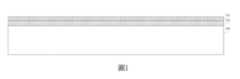
圖1-37描繪根據在此所述的某些實施例的在超音波晶片的裝置的利用製程的封裝期間的各種結構的橫截面。圖1是描繪耦接至載體基板106的釋放層104、以及耦接至該釋放層104的絕緣層102。該載體基板106例如可包含玻璃。該釋放層104例如可包含光熱轉換型(LTHC)塗料。該絕緣材料102例如可包含一種可以利用曝光及顯影而被圖案化的聚合物,例如是聚醯亞胺,聚苯並噁唑(PBO)、或是苯環丁烯(BCB)。FIGS. 1-37 depict cross-sections of various structures during packaging using a process of ultrasonic wafer devices, according to certain embodiments described herein. FIG. 1 depicts the
在圖2中,金屬層108被形成在該絕緣層102上。該金屬層108例如可以利用物理氣相沉積(PVD)或濺鍍來加以形成。該金屬層108例如可包含銅、或是在某些實施例中,該金屬層108可包含兩層,例如是耦接至該絕緣層102的鈦層、以及耦接至該鈦層的銅層。In FIG. 2, a
在圖3中,光阻層110被形成在該金屬層108上。例如,該光阻層110可包含光阻。In FIG. 3, a
在圖4中,開口被形成在該光阻層110中。例如,透過微影遮罩的曝光、接著是顯影可以在該光阻層110的透過該遮罩已被曝露到光的部分中產生開口。In FIG. 4, openings are formed in the
在圖5中,金屬柱112利用電鍍而被形成在該光阻層110中的開口內。該金屬層108可以作為用於該電鍍的晶種層。該些金屬柱112可包含和該金屬層108相同的材料,例如是銅。應該體認到的是,儘管四個金屬柱112被展示,但是可以有二維地配置的更多的金屬柱112(例如,數十個或是數百個)。In FIG. 5, the
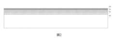
在圖6中,該光阻層110被移除。例如,光阻剝離液可被用來移除該光阻層110。該金屬層108的先前在該光阻層110的未曝光的部分之下的部分亦被移除。例如,非等向性蝕刻可被用來移除該金屬層108,其中該金屬層108比該些金屬柱112更快地被蝕刻。In FIG. 6, the
圖7是描繪耦接至絕緣層116的超音波晶片114。FIG. 7 depicts the
在圖8中,開口被產生在該絕緣層116中(例如,其利用微影)。In FIG. 8, openings are created in the insulating layer 116 (for example, it uses lithography).
在圖9中,光阻層118被形成在該絕緣層116上。In FIG. 9, a
在圖10中,開口被產生在該光阻層118中(例如,其利用微影),其中被產生在該光阻層118中的開口延伸到被產生在該絕緣層116中的開口之中。In FIG. 10, openings are created in the photoresist layer 118 (for example, it utilizes lithography), where the openings created in the
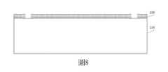
在圖11中,金屬接點120被形成在該光阻層118以及該絕緣層116中的開口之內。例如,該些金屬接點120可以藉由電鍍來加以形成,並且可包含銅或是一種銅合金。在某些實施例中,凸塊下金屬層(未顯示在圖11中)可被形成在該些金屬接點120以及該超音波晶片114之間。In FIG. 11,
在圖12中,該光阻層118被移除(例如,其利用光阻剝離液)。In FIG. 12, the
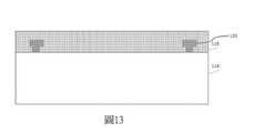
在圖13中,更多的絕緣材料被加到該絕緣層116,以覆蓋該些金屬接點120。In FIG. 13, more insulating material is added to the
在圖14中,晶粒附接膜(DAF)122耦接至該絕緣層102。In FIG. 14, a die attach film (DAF) 122 is coupled to the
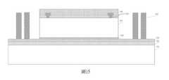
在圖15中,該超音波晶片114耦接至該晶粒附接膜122。In FIG. 15, the
在圖16中,囊封物124被形成以囊封該超音波晶片114、該絕緣層116、該晶粒附接膜122、以及該些金屬柱112。該囊封物124可包含模製化合物、模製底膠填充、環氧樹脂、或是樹脂。該囊封物124的頂表面延伸在該絕緣層116以及該些金屬柱112的頂表面之上。In FIG. 16, an
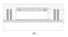
在圖17中,該囊封物124以及該絕緣層116的頂表面被平坦化,直到該些金屬柱112以及該金屬接點120的頂表面被露出為止。例如,化學機械平坦化(CMP)可被使用於該平坦化。In FIG. 17, the top surfaces of the
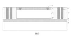
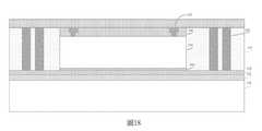
在圖18中,額外的絕緣材料被加到該絕緣層116,使得該絕緣層116覆蓋該些金屬接點120以及該些金屬柱112的頂表面。In FIG. 18, additional insulating material is added to the insulating
在圖19中,開口被產生在該些金屬接點120以及該些金屬柱112之上的絕緣層116中。例如,微影可被用來產生該些開口。In FIG. 19, openings are created in the insulating
在圖20中,重分佈線(RDL)126被形成在該絕緣層116中的開口中、以及在該絕緣層116上。如圖所示,該RDL 126可以電連接特定的金屬接點120至特定的金屬柱112。該RDL 126可包含金屬線路及貫孔,可以利用電鍍(包含一未被展示的晶種層的形成)來加以形成,並且可包含例如是鋁、銅、鎢的金屬、及/或這些金屬的合金。該RDL 126可包含多層的金屬線路及貫孔。In FIG. 20, a redistribution line (RDL) 126 is formed in the opening in the insulating
在圖21中,額外的絕緣材料被加到該絕緣層116以覆蓋該RDL 126的頂表面。In FIG. 21, additional insulating material is added to the insulating
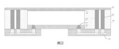
在圖22中,該載體基板106以及該釋放層104從該絕緣層102分離。例如,投射光(例如,紫外線或雷射)到該釋放層104之上可以分解該釋放層104,使得該釋放層104以及該載體基板106從該絕緣層102分離。該絕緣層102的表面亦可以被清洗以移除任何的殘留物。圖21的結構被翻轉以達成圖22的朝向。In FIG. 22, the
在圖23中,開口被產生在該絕緣層102中。In FIG. 23, openings are created in the insulating
在圖24中,焊料球128被設置在該絕緣層102中的開口內。在某些實施例中,該些焊料球128可以藉由電鍍來加以形成。在某些實施例中,其它形式的電連接器(例如,金屬柱)可被形成在該些開口中。在某些實施例中,凸塊下金屬層(未顯示在圖24中)可被形成在該些焊料球128以及該些金屬柱112之間。In FIG. 24,
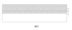
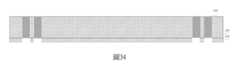
圖25描繪耦接至載體基板136的釋放層134、耦接至該釋放層134的絕緣層132、以及耦接至該絕緣層132的中介層130。該中介層130例如可包含鋁氮化物。FIG. 25 depicts the
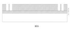
在圖26中,開口被形成在該中介層130中。例如,雷射鑽孔可被用來形成該些開口。In FIG. 26, openings are formed in the
在圖27中,金屬層138被形成在該中介層130上。該金屬層138例如可以利用濺鍍來加以形成。該金屬層138例如可包含銅、或是在某些實施例中,該金屬層138可包含兩層,例如是耦接至該中介層130的鈦層、以及耦接至該鈦層的銅層。In FIG. 27, the
在圖28中,金屬柱142利用電鍍而被形成在該中介層130中的開口內。該金屬層138可以作為用於該電鍍的晶種層。該些金屬柱142可包含和該金屬層138相同的材料,例如是銅。應該體認到的是,除了作為電性繞線之外,該些金屬柱142亦可以有助於加強可能是脆性的中介層130。In FIG. 28, the
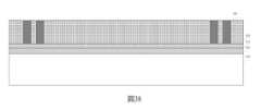
在圖29中,光阻層140被形成在該金屬層138以及該些金屬柱142上。In FIG. 29, a
在圖30中,該光阻層140被圖案化(例如,其係利用微影),以阻擋該些金屬柱142的頂表面。In FIG. 30, the
在圖31中,該金屬層108的未被阻擋的部分被蝕刻,以電性隔離該些金屬柱142。在某些實施例中,替代性的或額外的利用微影以阻擋該些金屬柱142,定時蝕刻或是非等向性蝕刻可被使用。In FIG. 31, the unblocked portion of the
在圖32中,該光阻層140被移除(例如,其利用光阻剝離液)。In FIG. 32, the
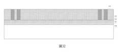
在圖33中,該載體基板136以及該釋放層134從該絕緣層132分離。In FIG. 33, the
在圖34中,開口被產生在該絕緣層132中。In FIG. 34, openings are created in the insulating
在圖35中,焊料球144被設置在該絕緣層132中的開口內。In FIG. 35,
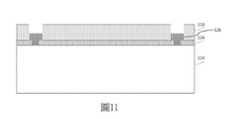
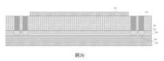
在圖36中,熱黏著層150耦接至該中介層130。在某些實施例中,該熱黏著層150可包含含銀的環氧樹脂。該些焊料球144耦接至印刷電路板(PCB)148。在某些實施例中,表面安裝技術(SMT)或是覆晶的焊接可被用來將該些焊料球144耦接至該PCB 148。底膠填充(例如,環氧樹脂)層146被形成在該絕緣層132以及該PCB 148之間。In FIG. 36, the thermal
在圖37中,該些焊料球128耦接至該些金屬柱142。該些金屬柱112與該些金屬柱142對準。在某些實施例中,表面安裝技術(SMT)或是覆晶的焊接可被用來將該些焊料球128耦接至該些金屬柱142。在該最終的結構中,該中介體可以提供在該超音波晶片114以及該PCB 148之間的電性繞線、以及用於該超音波晶片114的散熱器。In FIG. 37, the
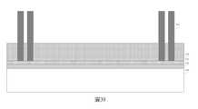
圖38-42係描繪根據在此所述的某些實施例的在超音波晶片的裝置的利用另一製程的封裝期間的各種結構的橫截面。圖38係描繪圖32的結構。FIGS. 38-42 depict cross-sections of various structures during packaging of another device of an ultrasonic wafer during packaging using another process, according to certain embodiments described herein. FIG. 38 depicts the structure of FIG. 32. FIG.
在圖39中,該些金屬柱142係利用電鍍而向上地延伸。如同可見的,該些金屬柱142延伸超出該中介層130的頂表面。In FIG. 39, the
在圖40中,該超音波晶片114透過該晶粒附接膜122來耦接至該中介層130。In FIG. 40, the
在圖41中,更多的絕緣材料被加到該絕緣層116。類似於在圖16中,該囊封物124被形成以囊封該超音波晶片114、該絕緣層116、該晶粒附接膜122、以及該些金屬柱142。類似於在圖18-21中,該RDL 126被形成。In FIG. 41, more insulating material is added to the insulating
在圖42中,類似於在圖33-36中,該載體基板136以及該釋放層134從該絕緣層132分離,該些焊料球144被形成在該些金屬柱142上,該些焊料球144耦接至該PCB 148,並且底膠填充層146被形成在該絕緣層132以及該PCB 148之間。In FIG. 42, similar to FIGS. 33-36, the
和圖1-37的製程相比較,圖38-42的製程可以使得該超音波晶片114能夠在製程控制、品質、以及良率可以是高的半導體晶圓代工中被結合到該中介層130。此外,儘管圖1-37的製程可能需要同時的該些焊料球128至該些金屬柱142的接合、以及該絕緣層102至該熱黏著劑150的接合,但是圖38-42的製程可以排除該熱黏著層150。Compared with the process of FIGS. 1-37, the process of FIGS. 38-42 can enable the
圖43描繪根據在此所述的某些實施例的用於封裝超音波晶片的範例的製程4300。在動作4302中,包含金屬柱的中介層耦接至印刷電路板。動作4302可以對應於在圖36中描繪的步驟。在動作4304中,該中介層耦接至包含金屬柱的經封裝的超音波晶片。動作4304可以對應於在圖37中描繪的步驟。該中介層可以透過熱黏著層來耦接至該經封裝的超音波晶片。FIG. 43 depicts an
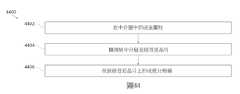
圖44描繪根據在此所述的某些實施例的用於封裝超音波晶片的範例的製程4400。在動作4402中,金屬柱被形成在中介層中。動作4402可以對應於在圖38-39中描繪的步驟。在動作4404中,該中介層耦接至超音波晶片。動作4404可以對應於在圖40中描繪的步驟。在動作4406中,重分佈層被形成在該經封裝的超音波晶片上。動作4406可以對應於在圖41中描繪的步驟。FIG. 44 depicts an
本揭露內容的各種特點可以單獨地、組合地、或是用並未在先前敘述的實施例中明確論述的各種配置來加以利用,並且因此在其應用上並未受限於在先前的說明中所闡述、或是在圖式中所描繪的構件的細節及配置。例如,在一實施例中敘述的特點可以用任何方式來和在其它實施例中敘述的特點組合。The various features of this disclosure can be utilized individually, in combination, or with various configurations that are not explicitly discussed in the previously described embodiments, and therefore their application is not limited to the previous description The details and configuration of the components described or depicted in the drawings. For example, features described in one embodiment can be combined with features described in other embodiments in any way.
除非另有清楚相反的指出,否則如同在此的說明書中以及在申請專利範圍中所用的該些不定冠詞“一”以及“一個”都應該被理解為表示“至少一個”。Unless clearly stated to the contrary, the indefinite articles "a" and "an" as used in the description herein and in the scope of patent application should be understood to mean "at least one".
如同在此的說明書中以及在申請專利範圍中所用的措辭"及/或"應該被理解為表示該些因此聯合的元件的"任一或是兩者",亦即元件在某些情形中是結合地存在,而在其它情形中則是分離地存在。利用“及/或”所表列的多個元件應該用相同的方式來加以解釋,亦即因此聯合的元件的“一或多個”。除了藉由該“及/或”子句明確所指出的元件之外的其它元件可以選配地存在,不論其是否相關或不相關那些明確所指出的元件。因此,作為一非限制性的例子,在一實施例中,一對於“A及/或B”的參照當結合例如是“包括”的開放式語言而被利用時可以是指只有A(選配地包含除了B以外的元件);在另一實施例中可以是指只有B(選配地包含除了A以外的元件);在又一實施例中可以是指A及B兩者(選配地包含其它元件);依此類推。The words "and/or" as used in this specification and in the scope of the patent application should be understood to mean "any or both" of the thus combined elements, ie the element is in some cases They exist in combination, but in other cases they exist separately. Multiple elements listed with "and/or" should be interpreted in the same way, that is to say "one or more" of the combined elements. Other elements than those explicitly indicated by the "and/or" clause may optionally exist, whether or not they are related or unrelated to those explicitly indicated. Therefore, as a non-limiting example, in an embodiment, a reference to "A and/or B" when used in conjunction with an open language such as "include" may refer to only A (optional) Contains elements other than B); in another embodiment, it can refer to only B (optionally contains elements other than A); in yet another embodiment, it can refer to both A and B (optionally Contains other components); and so on.
如同在此的說明書中以及在申請專利範圍中所用的,關於一或多個元件的一表列的措辭"至少一個"應該被理解為表示至少一選自該表列的元件中的任一個或多個元件之元件,但是不一定包含明確地被表列在該表列的元件內的每一個元件的至少一個,而且並不排除在該表列的元件中之元件的任意組合。此定義亦容許除了在該措辭"至少一個"所參照到的表列的元件之內明確所指出的元件之外的元件可以選配地存在,不論其是否相關或不相關那些明確所指出的元件。因此,作為一非限制性的例子,在一實施例中,“A及B中的至少一個”(或等同的是“A或B中的至少一個”、或等同的是“A及/或B中的至少一個”)可以是指至少一個(選配地包含超過一個)A,而沒有B存在(以及選配地包含除了B以外的元件);在另一實施例中可以是指至少一個(選配地包含超過一個)B,而沒有A存在(以及選配地包含除了A以外的元件);在又一實施例中可以是指至少一個(選配地包含超過一個)A與至少一個(選配地包含超過一個)B(以及選配地包含其它元件);依此類推。As used in the description herein and in the scope of patent applications, the wording "at least one" with respect to a list of one or more elements should be understood to mean at least one of the elements selected from the list or The elements of a plurality of elements do not necessarily include at least one of each element explicitly listed in the listed elements, and do not exclude any combination of the elements in the listed elements. This definition also allows elements other than those explicitly indicated within the listed elements referred to by the wording "at least one" to be optionally present, whether or not they are related or unrelated to those elements explicitly indicated . Therefore, as a non-limiting example, in one embodiment, "at least one of A and B" (or equivalently "at least one of A or B", or equivalently "A and/or B "At least one of" can mean at least one (optionally containing more than one) A, and no B is present (and optionally containing elements other than B); in another embodiment, it can mean at least one ( (Optionally contains more than one) B without A present (and optionally contains elements other than A); in yet another embodiment, it can mean at least one (optionally contains more than one) A and at least one ( Optionally contains more than one) B (and optionally contains other elements); and so on.
例如是“第一”、“第二”、“第三”、等等的序數術語在申請專利範圍中修飾一申請專利範圍元件的使用本身並不意味一申請專利範圍元件相對另一申請專利範圍元件的任何優先、在先或順序、或是一種方法的動作被執行所用的時間的順序,而是只被使用作為標籤來區別一具有某一名稱的申請專利範圍元件與另一具有一相同的名稱(但是為了該序數術語而使用)的元件,以區別該些申請專利範圍元件而已。Ordinal terms such as "first", "second", "third", etc. modify the use of a patent-scoped element within the scope of a patent application itself does not mean that a patent-scoped element is relative to another patent-scoped scope Any priority, precedence, or sequence of components, or the sequence of time it takes for a method's actions to be performed, but is only used as a label to distinguish between a patent-named component with a certain name and another with the same The elements of the name (but used for this ordinal term) are used to distinguish these patent-scoped elements.
如同在此所用的,對於一介於兩個端點之間的數值的參照應該被理解為涵蓋其中該數值可以具有該些端點的任一個的情況。例如,除非另有指出,否則陳述一特徵係具有一介於A到B之間或是介於約A到B之間的值應該被理解為表示所指出的範圍係包含該些端點A及B。As used herein, reference to a value between two end points should be understood to cover the case where the value may have any of the end points. For example, unless otherwise indicated, stating that a feature has a value between A and B or between about A and B should be understood to indicate that the indicated range includes the endpoints A and B .
該些術語“大約”及“大致”在某些實施例中可被用來表示在一目標值的±20%之內、在某些實施例中是在一目標值的±10%之內、在某些實施例中是在一目標值的±5%之內、以及另外在某些實施例中是在一目標值的±2%之內。該些術語“大約”及“大致”可包含該目標值。The terms "approximately" and "approximately" may be used in some embodiments to mean within ±20% of a target value, in certain embodiments within ±10% of a target value, In some embodiments it is within ±5% of a target value, and in certain embodiments it is within ±2% of a target value. The terms "about" and "approximately" may include the target value.
再者,在此使用的措辭及術語係為了說明之目的,因而不應該被視為限制性的。“包含”、“包括”、或是“具有”、“內含”、“涉及”、以及其變化的在此的使用係意謂涵蓋被列出在後面的項目及其等同物、以及額外的項目。Furthermore, the wording and terminology used herein are for the purpose of illustration and should not be regarded as limiting. The use of "including", "including", or "having", "inclusive", "involving", and variations thereof herein is meant to cover the items listed below and their equivalents, as well as additional project.
以上已經敘述至少一實施例的數個特點,將體認到的是各種的改變、修改、以及改良都將會輕易地被熟習此項技術者所思及。此種改變、修改、以及改良係欲為了此揭露內容之目的。於是,先前的說明及圖式只是舉例而已。Several features of at least one embodiment have been described above. It will be appreciated that various changes, modifications, and improvements will be easily considered by those skilled in the art. Such changes, modifications, and improvements are intended for the purpose of disclosing the content here. Therefore, the previous description and drawings are only examples.
102:絕緣層/絕緣材料104:釋放層106:載體基板108:金屬層110:光阻層112:金屬柱114:超音波晶片116:絕緣層118:光阻層120:金屬接點122:晶粒附接膜(DAF)124:囊封物126:重分佈線(RDL)128:焊料球130:中介層132:絕緣層134:釋放層136:載體基板138:金屬層140:光阻層142:金屬柱144:焊料球146:底膠填充層148:印刷電路板(PCB)150:熱黏著層/熱黏著劑4300:製程4302:動作4304:動作4400:製程4402:動作4404:動作4406:動作102: Insulation layer/insulation material104: release layer106: carrier substrate108: metal layer110: photoresist layer112: Metal pillar114: Ultrasonic chip116: Insulation118: photoresist layer120: Metal contacts122: Die Attach Film (DAF)124: Encapsulation126: Redistribution Line (RDL)128: solder ball130: intermediary layer132: Insulation134: Release layer136: carrier substrate138: metal layer140: photoresist layer142: Metal pillar144: solder ball146: Primer filling layer148: Printed Circuit Board (PCB)150: thermal adhesive layer/thermal adhesive4300: Process4302: Action4304: Action4400: Process4402: Action4404: Action4406: Action
各種的特點及實施例將會參考以下的範例且非限制性的圖來加以描述。應該體認到的是,該些圖並不一定按照比例繪製。出現在多個圖中的項目在它們出現的所有圖中都藉由相同或一類似的元件符號來加以指出。圖1-37描繪根據在此所述的某些實施例的在超音波晶片的裝置的利用一製程的封裝期間的各種結構的橫截面;圖38-42描繪根據在此所述的某些實施例的在超音波晶片的裝置的利用另一製程的封裝期間的各種結構的橫截面;圖43描繪根據在此所述的某些實施例的用於封裝超音波晶片的範例的製程;以及圖44描繪根據在此所述的某些實施例的用於封裝超音波晶片的範例的製程。Various features and embodiments will be described with reference to the following example and non-limiting drawings. It should be realized that these figures are not necessarily drawn to scale. Items that appear in multiple figures are indicated by the same or a similar component symbol in all figures where they appear.FIGS. 1-37 depict cross-sections of various structures during packaging of a device using a process according to certain embodiments described herein;FIGS. 38-42 depict cross-sections of various structures during packaging of another device of an ultrasonic wafer during packaging with another process according to certain embodiments described herein;43 depicts an exemplary process for packaging ultrasonic chips according to some embodiments described herein; andFIG. 44 depicts an example process for packaging ultrasonic chips according to some embodiments described herein.
102:絕緣層102: insulating layer
112:金屬柱112: Metal pillar
114:超音波晶片114: Ultrasonic chip
116:絕緣層116: Insulation
120:金屬接點120: Metal contacts
124:囊封物124: Encapsulation
126:重分佈線(RDL)126: Redistribution Line (RDL)
128:焊料球128: solder ball
130:中介層130: intermediary layer
132:絕緣層132: Insulation
142:金屬柱142: Metal pillar
144:焊料球144: solder ball
146:底膠填充層146: Primer filling layer
148:印刷電路板(PCB)148: Printed Circuit Board (PCB)
150:熱黏著層150: thermal adhesive layer
Claims (29)
Translated fromChineseApplications Claiming Priority (2)
| Application Number | Priority Date | Filing Date | Title |
|---|---|---|---|
| US201862694810P | 2018-07-06 | 2018-07-06 | |
| US62/694,810 | 2018-07-06 |
Publications (1)
| Publication Number | Publication Date |
|---|---|
| TW202011897Atrue TW202011897A (en) | 2020-04-01 |
Family
ID=69059840
Family Applications (1)
| Application Number | Title | Priority Date | Filing Date |
|---|---|---|---|
| TW108123485ATW202011897A (en) | 2018-07-06 | 2019-07-03 | Methods and apparatuses for packaging an ultrasound-on-a-chip |
Country Status (9)
| Country | Link |
|---|---|
| US (2) | US11018068B2 (en) |
| EP (1) | EP3818372B1 (en) |
| JP (1) | JP2021529459A (en) |
| KR (1) | KR20210030951A (en) |
| CN (1) | CN112368574B (en) |
| AU (1) | AU2019297412A1 (en) |
| CA (1) | CA3105492A1 (en) |
| TW (1) | TW202011897A (en) |
| WO (1) | WO2020010207A1 (en) |
Families Citing this family (18)
| Publication number | Priority date | Publication date | Assignee | Title |
|---|---|---|---|---|
| EP3788798B1 (en) | 2018-05-03 | 2023-07-05 | BFLY Operations, Inc. | Ultrasonic transducers with pressure ports |
| KR20210030951A (en) | 2018-07-06 | 2021-03-18 | 버터플라이 네트워크, 인크. | Method and apparatus for packaging ultrasonic-on-chip |
| AU2019350989A1 (en) | 2018-09-28 | 2021-03-25 | Butterfly Network, Inc. | Fabrication techniques and structures for gettering materials in ultrasonic transducer cavities |
| US11626343B2 (en)* | 2018-10-30 | 2023-04-11 | Taiwan Semiconductor Manufacturing Co., Ltd. | Semiconductor device with enhanced thermal dissipation and method for making the same |
| US11638931B2 (en) | 2018-11-13 | 2023-05-02 | Bfly Operations, Inc. | Getter technology for micromachined ultrasonic transducer cavities |
| WO2020102492A1 (en) | 2018-11-15 | 2020-05-22 | Butterfly Network, Inc. | Anti-stiction bottom cavity surface for micromachined ultrasonic transducer devices |
| CA3121805A1 (en) | 2018-12-07 | 2020-06-11 | Octant, Inc. | Systems for protein-protein interaction screening |
| TW202045099A (en) | 2019-02-07 | 2020-12-16 | 美商蝴蝶網路公司 | Bi-layer metal electrode for micromachined ultrasonic transducer devices |
| EP3930923A4 (en) | 2019-02-25 | 2023-01-11 | Bfly Operations, Inc. | Adaptive cavity thickness control for micromachined ultrasonic transducer devices |
| WO2020210470A1 (en) | 2019-04-12 | 2020-10-15 | Butterfly Network, Inc. | Bottom electrode via structures for micromachined ultrasonic transducer devices |
| US11501562B2 (en) | 2019-04-30 | 2022-11-15 | Bfly Operations, Inc. | Ultrasound face scanning and identification apparatuses and methods |
| US11684951B2 (en) | 2019-08-08 | 2023-06-27 | Bfly Operations, Inc. | Micromachined ultrasonic transducer devices having truncated circle shaped cavities |
| US11676922B2 (en)* | 2019-10-28 | 2023-06-13 | Qualcomm Incorporated | Integrated device comprising interconnect structures having an inner interconnect, a dielectric layer and a conductive layer |
| US11988640B2 (en) | 2020-03-11 | 2024-05-21 | Bfly Operations, Inc. | Bottom electrode material stack for micromachined ultrasonic transducer devices |
| US11776820B2 (en) | 2020-09-30 | 2023-10-03 | Huawei Technologies Co., Ltd. | Vertical interconnection structure and manufacturing method thereof, packaged chip, and chip packaging method |
| TW202240165A (en) | 2021-03-04 | 2022-10-16 | 美商蝴蝶營運公司 | Micromachined ultrasound transducer with pedestal |
| TW202239483A (en) | 2021-03-04 | 2022-10-16 | 美商蝴蝶營運公司 | Capacitive micromachined ultrasonic transducers (cmuts) having non-uniform pedestals |
| US12156762B2 (en) | 2021-04-01 | 2024-12-03 | Bfly Operations, Inc. | Apparatuses and methods for configuring ultrasound devices |
Family Cites Families (33)
| Publication number | Priority date | Publication date | Assignee | Title |
|---|---|---|---|---|
| US7327554B2 (en)* | 2003-03-19 | 2008-02-05 | Ngk Spark Plug Co., Ltd. | Assembly of semiconductor device, interposer and substrate |
| US20060055024A1 (en)* | 2004-09-14 | 2006-03-16 | Staktek Group, L.P. | Adapted leaded integrated circuit module |
| US7741686B2 (en) | 2006-07-20 | 2010-06-22 | The Board Of Trustees Of The Leland Stanford Junior University | Trench isolated capacitive micromachined ultrasonic transducer arrays with a supporting frame |
| DE102007026445A1 (en) | 2007-06-06 | 2008-12-11 | Robert Bosch Gmbh | Micromechanical component and method for producing a micromechanical component |
| US8193685B2 (en) | 2007-07-03 | 2012-06-05 | Koninklijke Philips Electronics N.V. | Thin film detector for presence detection |
| US7843022B2 (en) | 2007-10-18 | 2010-11-30 | The Board Of Trustees Of The Leland Stanford Junior University | High-temperature electrostatic transducers and fabrication method |
| US7781238B2 (en) | 2007-12-06 | 2010-08-24 | Robert Gideon Wodnicki | Methods of making and using integrated and testable sensor array |
| US20110055447A1 (en) | 2008-05-07 | 2011-03-03 | Signostics Limited | Docking system for medical diagnostic scanning using a handheld device |
| US7838337B2 (en)* | 2008-12-01 | 2010-11-23 | Stats Chippac, Ltd. | Semiconductor device and method of forming an interposer package with through silicon vias |
| US7790492B1 (en) | 2009-06-13 | 2010-09-07 | Mwm Acoustics, Llc | Method for fabricating a transducer package with the transducer die unsupported by a substrate |
| US8207652B2 (en) | 2009-06-16 | 2012-06-26 | General Electric Company | Ultrasound transducer with improved acoustic performance |
| US20130237055A1 (en)* | 2010-06-11 | 2013-09-12 | Imec | Method of redistributing functional element |
| TWI667700B (en) | 2010-12-01 | 2019-08-01 | 美商1366科技公司 | Making semiconductor bodies from molten material using a free-standing interposer sheet |
| US8614488B2 (en)* | 2010-12-08 | 2013-12-24 | Ying-Nan Wen | Chip package and method for forming the same |
| CN105188960A (en) | 2013-02-05 | 2015-12-23 | 声音技术公司 | Ultrasound device |
| US9533873B2 (en) | 2013-02-05 | 2017-01-03 | Butterfly Network, Inc. | CMOS ultrasonic transducers and related apparatus and methods |
| EP4122609B1 (en) | 2013-03-15 | 2024-11-06 | BFLY Operations, Inc. | Complementary metal oxide semiconductor (cmos) ultrasonic transducers and methods for forming the same |
| US9633869B2 (en)* | 2013-08-16 | 2017-04-25 | Taiwan Semiconductor Manufacturing Company, Ltd. | Packages with interposers and methods for forming the same |
| AU2015247484B2 (en) | 2014-04-18 | 2020-05-14 | Butterfly Network, Inc. | Ultrasonic transducers in complementary metal oxide semiconductor (CMOS) wafers and related apparatus and methods |
| US9252127B1 (en) | 2014-07-10 | 2016-02-02 | Invensas Corporation | Microelectronic assemblies with integrated circuits and interposers with cavities, and methods of manufacture |
| US9067779B1 (en)* | 2014-07-14 | 2015-06-30 | Butterfly Network, Inc. | Microfabricated ultrasonic transducers and related apparatus and methods |
| US20160009544A1 (en)* | 2015-03-02 | 2016-01-14 | Butterfly Network, Inc. | Microfabricated ultrasonic transducers and related apparatus and methods |
| US10276541B2 (en)* | 2015-06-30 | 2019-04-30 | Taiwan Semiconductor Manufacturing Company, Ltd. | 3D package structure and methods of forming same |
| TWI721183B (en)* | 2016-06-20 | 2021-03-11 | 美商蝴蝶網路公司 | Electrical contact arrangement for microfabricated ultrasonic transducer |
| US9922896B1 (en) | 2016-09-16 | 2018-03-20 | Taiwan Semiconductor Manufacturing Company, Ltd. | Info structure with copper pillar having reversed profile |
| CN106449554B (en)* | 2016-12-06 | 2019-12-17 | 苏州源戍微电子科技有限公司 | chip embedded packaging structure with closed cavity and manufacturing method thereof |
| US10196261B2 (en) | 2017-03-08 | 2019-02-05 | Butterfly Network, Inc. | Microfabricated ultrasonic transducers and related apparatus and methods |
| WO2018236956A1 (en) | 2017-06-21 | 2018-12-27 | Butterfly Network, Inc. | MICROFABRICATED ULTRASONIC TRANSDUCER HAVING INDIVIDUAL CELLS HAVING ELECTRICALLY ISOLATED ELECTRODE SECTIONS |
| CN108155160A (en)* | 2018-01-29 | 2018-06-12 | 中芯长电半导体(江阴)有限公司 | The encapsulating structure and packaging method of fingerprint recognition chip |
| JP2021511750A (en) | 2018-01-30 | 2021-05-06 | バタフライ ネットワーク,インコーポレイテッド | Methods and equipment for packaging ultrasonic on-chips |
| TW201938834A (en) | 2018-03-09 | 2019-10-01 | 美商蝴蝶網路公司 | Ultrasound transducer devices and methods for fabricating ultrasound transducer devices |
| TW201947717A (en) | 2018-05-03 | 2019-12-16 | 美商蝴蝶網路公司 | Vertical packaging for ultrasound-on-a-chip and related methods |
| KR20210030951A (en)* | 2018-07-06 | 2021-03-18 | 버터플라이 네트워크, 인크. | Method and apparatus for packaging ultrasonic-on-chip |
- 2019
- 2019-07-03KRKR1020217003420Apatent/KR20210030951A/ennot_activeCeased
- 2019-07-03JPJP2020571590Apatent/JP2021529459A/enactivePending
- 2019-07-03AUAU2019297412Apatent/AU2019297412A1/ennot_activeAbandoned
- 2019-07-03WOPCT/US2019/040516patent/WO2020010207A1/ennot_activeCeased
- 2019-07-03EPEP19830619.3Apatent/EP3818372B1/enactiveActive
- 2019-07-03TWTW108123485Apatent/TW202011897A/enunknown
- 2019-07-03CACA3105492Apatent/CA3105492A1/enactivePending
- 2019-07-03USUS16/502,553patent/US11018068B2/enactiveActive
- 2019-07-03CNCN201980045060.6Apatent/CN112368574B/enactiveActive
- 2021
- 2021-03-04USUS17/191,829patent/US11676874B2/enactiveActive
Also Published As
| Publication number | Publication date |
|---|---|
| US20200013691A1 (en) | 2020-01-09 |
| AU2019297412A1 (en) | 2021-01-28 |
| CN112368574B (en) | 2023-08-01 |
| US11676874B2 (en) | 2023-06-13 |
| KR20210030951A (en) | 2021-03-18 |
| JP2021529459A (en) | 2021-10-28 |
| US11018068B2 (en) | 2021-05-25 |
| CN112368574A (en) | 2021-02-12 |
| US20210296195A1 (en) | 2021-09-23 |
| EP3818372A1 (en) | 2021-05-12 |
| WO2020010207A1 (en) | 2020-01-09 |
| EP3818372A4 (en) | 2022-04-06 |
| EP3818372B1 (en) | 2024-10-30 |
| CA3105492A1 (en) | 2020-01-09 |
| EP3818372C0 (en) | 2024-10-30 |
Similar Documents
| Publication | Publication Date | Title |
|---|---|---|
| TW202011897A (en) | Methods and apparatuses for packaging an ultrasound-on-a-chip | |
| US11694943B2 (en) | Semiconductor device including heat dissipation structure and fabricating method of the same | |
| CN107731787B (en) | Semiconductor device package and stacked package assembly including high density interconnects | |
| US10978346B2 (en) | Conductive vias in semiconductor packages and methods of forming same | |
| TWI735702B (en) | Integrated fan-out package and manufacturing method thereof | |
| TWI685079B (en) | Interposers with circuit modules encapsulated by moldable material in a cavity, and methods of fabrication | |
| US20210398942A1 (en) | Integrated fan-out package and manufacturing method thereof | |
| US10290605B2 (en) | Fan-out package structure and method for forming the same | |
| TW201926489A (en) | Package method and device same | |
| TW201906115A (en) | Integrated fan-out package and forming method thereof | |
| US9633924B1 (en) | Package structure and method for forming the same | |
| KR102459551B1 (en) | Cowos structures and methods forming same | |
| CN107481942B (en) | Integrated fan-out structure with rugged interconnects | |
| TW201133743A (en) | Semiconductor structure and method forming semiconductor device | |
| US10978405B1 (en) | Integrated fan-out package | |
| CN108269767A (en) | Method for forming chip structure on substrate wafer | |
| JP4115326B2 (en) | Manufacturing method of semiconductor package | |
| TW202013650A (en) | Method for forming chip package structure | |
| US11114359B2 (en) | Wafer level chip scale package structure | |
| CN113130414A (en) | Wafer-level 3D packaging structure and preparation method thereof | |
| TW202422710A (en) | Packages with inductor dies and methods forming the same | |
| TW202339133A (en) | Packages and manufacturing method thereof | |
| US20210288005A1 (en) | Semiconductor package | |
| TW202510267A (en) | Integrated circuit |