TW202011687A - Radio-frequency coil signal chain for a low-field MRI system - Google Patents
Radio-frequency coil signal chain for a low-field MRI systemDownload PDFInfo
- Publication number
- TW202011687A TW202011687ATW108117535ATW108117535ATW202011687ATW 202011687 ATW202011687 ATW 202011687ATW 108117535 ATW108117535 ATW 108117535ATW 108117535 ATW108117535 ATW 108117535ATW 202011687 ATW202011687 ATW 202011687A
- Authority
- TW
- Taiwan
- Prior art keywords
- coil
- circuit
- substrate
- fet
- amplifier
- Prior art date
Links
Images


Classifications
- G—PHYSICS
- G01—MEASURING; TESTING
- G01R—MEASURING ELECTRIC VARIABLES; MEASURING MAGNETIC VARIABLES
- G01R33/00—Arrangements or instruments for measuring magnetic variables
- G01R33/0023—Electronic aspects, e.g. circuits for stimulation, evaluation, control; Treating the measured signals; calibration
- G01R33/0029—Treating the measured signals, e.g. removing offset or noise
- G—PHYSICS
- G01—MEASURING; TESTING
- G01R—MEASURING ELECTRIC VARIABLES; MEASURING MAGNETIC VARIABLES
- G01R33/00—Arrangements or instruments for measuring magnetic variables
- G01R33/20—Arrangements or instruments for measuring magnetic variables involving magnetic resonance
- G01R33/28—Details of apparatus provided for in groups G01R33/44 - G01R33/64
- G01R33/32—Excitation or detection systems, e.g. using radio frequency signals
- G01R33/34—Constructional details, e.g. resonators, specially adapted to MR
- G01R33/34007—Manufacture of RF coils, e.g. using printed circuit board technology; additional hardware for providing mechanical support to the RF coil assembly or to part thereof, e.g. a support for moving the coil assembly relative to the remainder of the MR system
- G—PHYSICS
- G01—MEASURING; TESTING
- G01R—MEASURING ELECTRIC VARIABLES; MEASURING MAGNETIC VARIABLES
- G01R33/00—Arrangements or instruments for measuring magnetic variables
- G01R33/20—Arrangements or instruments for measuring magnetic variables involving magnetic resonance
- G01R33/28—Details of apparatus provided for in groups G01R33/44 - G01R33/64
- G01R33/32—Excitation or detection systems, e.g. using radio frequency signals
- G01R33/34—Constructional details, e.g. resonators, specially adapted to MR
- G01R33/34046—Volume type coils, e.g. bird-cage coils; Quadrature bird-cage coils; Circularly polarised coils
- G01R33/34053—Solenoid coils; Toroidal coils
- G—PHYSICS
- G01—MEASURING; TESTING
- G01R—MEASURING ELECTRIC VARIABLES; MEASURING MAGNETIC VARIABLES
- G01R33/00—Arrangements or instruments for measuring magnetic variables
- G01R33/20—Arrangements or instruments for measuring magnetic variables involving magnetic resonance
- G01R33/28—Details of apparatus provided for in groups G01R33/44 - G01R33/64
- G01R33/32—Excitation or detection systems, e.g. using radio frequency signals
- G01R33/34—Constructional details, e.g. resonators, specially adapted to MR
- G01R33/341—Constructional details, e.g. resonators, specially adapted to MR comprising surface coils
- G—PHYSICS
- G01—MEASURING; TESTING
- G01R—MEASURING ELECTRIC VARIABLES; MEASURING MAGNETIC VARIABLES
- G01R33/00—Arrangements or instruments for measuring magnetic variables
- G01R33/20—Arrangements or instruments for measuring magnetic variables involving magnetic resonance
- G01R33/28—Details of apparatus provided for in groups G01R33/44 - G01R33/64
- G01R33/32—Excitation or detection systems, e.g. using radio frequency signals
- G01R33/36—Electrical details, e.g. matching or coupling of the coil to the receiver
- G01R33/3614—RF power amplifiers
- G—PHYSICS
- G01—MEASURING; TESTING
- G01R—MEASURING ELECTRIC VARIABLES; MEASURING MAGNETIC VARIABLES
- G01R33/00—Arrangements or instruments for measuring magnetic variables
- G01R33/20—Arrangements or instruments for measuring magnetic variables involving magnetic resonance
- G01R33/28—Details of apparatus provided for in groups G01R33/44 - G01R33/64
- G01R33/32—Excitation or detection systems, e.g. using radio frequency signals
- G01R33/36—Electrical details, e.g. matching or coupling of the coil to the receiver
- G01R33/3628—Tuning/matching of the transmit/receive coil
- G—PHYSICS
- G01—MEASURING; TESTING
- G01R—MEASURING ELECTRIC VARIABLES; MEASURING MAGNETIC VARIABLES
- G01R33/00—Arrangements or instruments for measuring magnetic variables
- G01R33/20—Arrangements or instruments for measuring magnetic variables involving magnetic resonance
- G01R33/28—Details of apparatus provided for in groups G01R33/44 - G01R33/64
- G01R33/32—Excitation or detection systems, e.g. using radio frequency signals
- G01R33/36—Electrical details, e.g. matching or coupling of the coil to the receiver
- G01R33/3642—Mutual coupling or decoupling of multiple coils, e.g. decoupling of a receive coil from a transmission coil, or intentional coupling of RF coils, e.g. for RF magnetic field amplification
- G01R33/3657—Decoupling of multiple RF coils wherein the multiple RF coils do not have the same function in MR, e.g. decoupling of a transmission coil from a receive coil
- G—PHYSICS
- G01—MEASURING; TESTING
- G01R—MEASURING ELECTRIC VARIABLES; MEASURING MAGNETIC VARIABLES
- G01R33/00—Arrangements or instruments for measuring magnetic variables
- G01R33/20—Arrangements or instruments for measuring magnetic variables involving magnetic resonance
- G01R33/28—Details of apparatus provided for in groups G01R33/44 - G01R33/64
- G01R33/38—Systems for generation, homogenisation or stabilisation of the main or gradient magnetic field
- G01R33/385—Systems for generation, homogenisation or stabilisation of the main or gradient magnetic field using gradient magnetic field coils
- G01R33/3854—Systems for generation, homogenisation or stabilisation of the main or gradient magnetic field using gradient magnetic field coils means for active and/or passive vibration damping or acoustical noise suppression in gradient magnet coil systems
- G—PHYSICS
- G01—MEASURING; TESTING
- G01R—MEASURING ELECTRIC VARIABLES; MEASURING MAGNETIC VARIABLES
- G01R33/00—Arrangements or instruments for measuring magnetic variables
- G01R33/20—Arrangements or instruments for measuring magnetic variables involving magnetic resonance
- G01R33/44—Arrangements or instruments for measuring magnetic variables involving magnetic resonance using nuclear magnetic resonance [NMR]
- G01R33/445—MR involving a non-standard magnetic field B0, e.g. of low magnitude as in the earth's magnetic field or in nanoTesla spectroscopy, comprising a polarizing magnetic field for pre-polarisation, B0 with a temporal variation of its magnitude or direction such as field cycling of B0 or rotation of the direction of B0, or spatially inhomogeneous B0 like in fringe-field MR or in stray-field imaging
- G—PHYSICS
- G01—MEASURING; TESTING
- G01R—MEASURING ELECTRIC VARIABLES; MEASURING MAGNETIC VARIABLES
- G01R33/00—Arrangements or instruments for measuring magnetic variables
- G01R33/20—Arrangements or instruments for measuring magnetic variables involving magnetic resonance
- G01R33/44—Arrangements or instruments for measuring magnetic variables involving magnetic resonance using nuclear magnetic resonance [NMR]
- G01R33/48—NMR imaging systems
- G01R33/54—Signal processing systems, e.g. using pulse sequences ; Generation or control of pulse sequences; Operator console
- G01R33/56—Image enhancement or correction, e.g. subtraction or averaging techniques, e.g. improvement of signal-to-noise ratio and resolution
- G01R33/565—Correction of image distortions, e.g. due to magnetic field inhomogeneities
Landscapes
- Physics & Mathematics (AREA)
- Condensed Matter Physics & Semiconductors (AREA)
- General Physics & Mathematics (AREA)
- High Energy & Nuclear Physics (AREA)
- Spectroscopy & Molecular Physics (AREA)
- General Health & Medical Sciences (AREA)
- Health & Medical Sciences (AREA)
- Nuclear Medicine, Radiotherapy & Molecular Imaging (AREA)
- Radiology & Medical Imaging (AREA)
- Engineering & Computer Science (AREA)
- Signal Processing (AREA)
- Magnetic Resonance Imaging Apparatus (AREA)
- Amplifiers (AREA)
Abstract
Description
Translated fromChinese本申請案係關於用於一低場MRI系統之射頻線圈信號鏈。This application is related to a radio frequency coil signal chain used in a low field MRI system.
磁共振成像(MRI)為眾多應用提供一重要成像模態且廣泛用於臨床及研究環境中以產生人體內部之影像。作為一一般性,MRI係基於偵測磁共振(MR)信號,該等磁共振(MR)信號係由原子回應於經施加電磁場產生之狀態改變而發射之電磁波。舉例而言,核磁共振(NMR)技術涉及在一正成像之物件中之原子(例如,人體之組織中之原子)之核自旋之重新對準或馳豫之後旋即偵測自受激原子之原子核發射之MR信號。所偵測MR信號可經處理以產生影像,在醫學應用之內容脈絡中,此允許出於診斷、治療及/或研究目的研究身體內之內部結構及/或生物程序。Magnetic resonance imaging (MRI) provides an important imaging modality for many applications and is widely used in clinical and research environments to generate images of the human body. As a generality, MRI is based on detecting magnetic resonance (MR) signals, which are electromagnetic waves emitted by atoms in response to changes in state generated by the applied electromagnetic field. For example, nuclear magnetic resonance (NMR) technology involves the realignment or relaxation of the nuclear spins of atoms in an object being imaged (eg, atoms in tissues of the human body), and the detection of excited atoms immediately afterwards. The MR signal emitted by the atomic nucleus. The detected MR signals can be processed to produce images, in the context of medical applications, which allows the study of internal structures and/or biological procedures within the body for diagnostic, therapeutic and/or research purposes.
歸因於在無需其他模態之安全關切之情形下(例如,無需將受試者曝露於離子化輻射,例如x射線,或將放射性材料引入至身體之情形下)產生具有相對高解析度及反差比之非侵入性影像之能力,MRI為生物成像提供一種具吸引力之成像模態。此外,MRI尤其適合於提供軟組織反差比,其可經利用以使其他成像模態不能令人滿足地成像之標的物成像。此外,MR技術能夠擷取關於其他模態不能獲取之結構及/或生物程序之資訊。然而,MRI存在若干個缺點,對於一既定成像應用,該等缺點可涉及設備之相對高成本、受限制之可用性及/或獲得臨床MRI掃描器之難度及/或影像獲取程序之長度。Attributable to situations where safety concerns of other modalities are not required (for example, it is not necessary to expose the subject to ionizing radiation, such as x-rays, or to introduce radioactive materials into the body) with relatively high resolution and The ability of contrast ratio to non-invasive imaging, MRI provides an attractive imaging modality for biological imaging. In addition, MRI is particularly suitable for providing soft tissue contrast ratios, which can be utilized to image objects that are not satisfactorily imaged by other imaging modalities. In addition, MR technology can capture information about structures and/or biological procedures that are not available in other modalities. However, MRI has several disadvantages. For a given imaging application, these disadvantages may involve the relatively high cost of the equipment, limited availability, and/or the difficulty of obtaining a clinical MRI scanner and/or the length of the image acquisition procedure.
臨床MRI之趨勢係增加MRI掃描器之場強度以改良掃描時間、影像解析度及影像反差比中之一或多者,此繼而繼續推高成本。絕大多數經安裝MRI掃描器在1.5或3特士拉(T)下操作,特士拉係指主磁場B0之場強度。一臨床MRI掃描器之一粗略成本估計係大約每特士拉一百萬美元,此未考慮操作此等MRI掃描器所涉及的大量操作、維護及維修成本。The trend in clinical MRI is to increase the field strength of MRI scanners to improve one or more of scan time, image resolution, and image contrast ratio, which in turn continues to drive up costs. Most installed MRI scanners operate at 1.5 or 3 Tesla (T), which refers to the field strength of the main magnetic field B0 . The rough cost of one of the clinical MRI scanners is estimated to be about one million US dollars per tesla. This does not take into account the large operation, maintenance and repair costs involved in operating these MRI scanners.
此外,習用高場MRI系統通常需要大的超導磁體及相關聯電子裝置以產生一物件(例如,一病患)在其中成像之一強均勻靜磁場(B0)。此等系統之大小係相當大的,其中一典型MRI設施包含用於磁體、電子裝置、熱管理系統及控制台區域之多個房間。MRI系統之大小及開支一般而言將其使用限制於諸如醫院及學術研究中心之公共設施,此等公共設施具有充足空間及資源來購買及維持MRI系統。高場MRI系統之高成本及大量空間要求導致MRI掃描器之受限制可用性。如此,經常存在其中一MRI掃描將係有益的之臨床情形,但歸因於上文所論述之限制中之一或多者,此係不實務的或係不可能的,如下文進一步詳細論述。In addition, conventional high-field MRI systems generally require large superconducting magnets and associated electronic devices to generate a strong uniform static magnetic field (B0 ) in which an object (eg, a patient) is imaged. The size of these systems is quite large, and a typical MRI facility includes multiple rooms for magnets, electronic devices, thermal management systems, and console areas. The size and expenses of MRI systems generally limit their use to public facilities such as hospitals and academic research centers, which have sufficient space and resources to purchase and maintain MRI systems. The high cost and large space requirements of high-field MRI systems result in limited availability of MRI scanners. As such, there are often clinical situations where one of the MRI scans will be beneficial, but due to one or more of the limitations discussed above, this is not practical or possible, as discussed in further detail below.
某些實施例包含一開關電路,其經組態以耦合至一低場磁共振成像系統之一射頻(RF)線圈。該開關電路包括至少一個場效應電晶體(FET),其經組態以在小於10 MHz之一操作頻率下作為一RF開關而操作。Some embodiments include a switching circuit configured to be coupled to a radio frequency (RF) coil of a low field magnetic resonance imaging system. The switching circuit includes at least one field effect transistor (FET) configured to operate as an RF switch at an operating frequency of less than 10 MHz.
某些實施例包含一電路,其經組態以調諧耦合至一低場磁共振成像系統之一放大器之一射頻(RF)線圈。該電路包括:調諧電路,其跨越該放大器之輸入而耦合;及主動回饋電路,其耦合於該放大器之一輸出與該放大器之一輸入之間,其中該主動回饋電路包含一回饋電容器。Some embodiments include a circuit configured to tune and couple to a radio frequency (RF) coil of an amplifier of a low field magnetic resonance imaging system. The circuit includes: a tuning circuit coupled across the input of the amplifier; and an active feedback circuit coupled between an output of the amplifier and an input of the amplifier, wherein the active feedback circuit includes a feedback capacitor.
某些實施例包含一電路,其經組態以調諧耦合至一低場磁共振成像系統之一放大器之一射頻(RF)線圈。該電路包括主動回饋電路,其耦合於該放大器之一輸出與該放大器之一輸入之間以減少該RF線圈一品質因子。Some embodiments include a circuit configured to tune and couple to a radio frequency (RF) coil of an amplifier of a low field magnetic resonance imaging system. The circuit includes an active feedback circuit coupled between an output of the amplifier and an input of the amplifier to reduce a quality factor of the RF coil.
本申請案依據35 U.S.C. § 119(e)主張於2018年5月21日提出申請且標題為「用於低場MRI系統之射頻線圈信號鏈(Radio-frequency Coil Signal Chain for a Low-field MRI System)」之美國臨時專利申請案第62/674,458號以及於2018年6月29日提出申請且標題為「用於低場MRI系統之射頻線圈信號鏈(Radio-frequency Coil Signal Chain for a Low-field MRI System)」之美國臨時專利申請案第62/692,454號之優先權,該等申請案中之每一者之全部內容以引用方式併入本文中。This application is based on 35 USC § 119(e), which claims to apply on May 21, 2018 and is titled ``Radio-frequency Coil Signal Chain for a Low-field MRI System )’S U.S. Provisional Patent Application No. 62/674,458 and filed on June 29, 2018 and titled ``Radio-frequency Coil Signal Chain for a Low-field MRI System MRI System) of US Provisional Patent Application No. 62/692,454, the entire contents of each of these applications are incorporated herein by reference.
MRI掃描器市場由高場系統且特定而言醫療或臨床MRI應用壓倒性地主導。如上文所論述,醫療成像中之一般趨勢係產生具有越來越大場強度之MRI掃描器,其中絕大多數臨床MRI掃描器在1.5 T或3 T下操作,其中在研究環境中使用7 T及9 T之較高場強度。如本文中所使用,「高場」一般而言係指在一臨床環境中當前在使用中之MRI系統,且更特定而言,係指在1.5 T或高於1.5 T之一主磁場(亦即,一B0場)下操作之MRI系統,儘管在0.5 T與1.5 T之間操作之臨床系統亦通常表徵為「高場」。在大約0.2 T與0.5 T之間之場強度已表徵為「中場」,並且,隨著高場型態中之場強度繼續增加,在0.5 T與1 T之間之範圍中之場強度亦已表徵為中場。相比而言,「低場」一般而言係指以小於或等於大約0.2 T之一B0場操作之MRI系統,儘管由於高場型態之高端處之經增加場強度,具有介於0.2 T與大約0.3 T之間之一B0場之系統有時已表徵為低場。在低場型態內,以小於0.1 T之一B0場操作之低場MRI系統在本文中被稱為「極低場」且以小於10 mT之一B0場操作之低場MRI系統在本文中被稱為「超低場」。The MRI scanner market is dominated by high-field systems and in particular medical or clinical MRI applications. As discussed above, the general trend in medical imaging is to produce MRI scanners with increasing field strength. Most of the clinical MRI scanners operate at 1.5 T or 3 T, of which 7 T and 7 are used in the research environment. 9 T higher field strength. As used herein, "high field" generally refers to an MRI system currently in use in a clinical environment, and more specifically, refers to a main magnetic field at or above 1.5 T (also That is, an MRI system operated under a B0 field), although a clinical system operated between 0.5 T and 1.5 T is usually characterized as a “high field”. The field strength between about 0.2 T and 0.5 T has been characterized as a “midfield”, and as the field strength in the high field pattern continues to increase, the field strength in the range between 0.5 T and 1 T also Has been characterized as a midfielder. In contrast, "low field" generally refers to an MRI system operating at a B0 field of less than or equal to approximately 0.2 T, although due to the increased field strength at the high end of the high field type, it has a value between 0.2 A system with a B0 field between T and approximately 0.3 T has sometimes been characterized as a low field. In the low-field type, a low-field MRI system operating with a B0 field of less than 0.1 T is referred to herein as a “very low field” and a low-field MRI system operating with a B0 field of less than 10 mT. This article is called "ultra-low field".
如上文所論述,習用MRI系統需要專門化公共設施。MRI系統之操作需要一電磁屏蔽房間且該房間之地板必須在結構上增強。必須為高功率電子裝置及掃描技術人員之控制區域提供額外房間。亦必須提供站點之安全通道。此外,必須安裝一專用三相電連接以為電子裝置提供電力,該等電子裝置又由一冷凍水供應器冷卻。通常亦必須提供額外HVAC容量。此等站點要求不僅係昂貴的,且顯著限制其中可部署MRI系統之位置。習用臨床MRI掃描器亦需要大量專業技術來操作及維持。此等經高度訓練之技術人員及服務工程師添加大的持續操作成本以操作一MRI系統。因此,習用MRI頻繁地受到成本過高限制且嚴重受限於易達性,從而妨礙MRI成為能夠隨時隨地交付一寬範圍臨床成像解決方案之一廣泛可用之診斷工具。通常,一病患必須在預先排程之一時間及地點處訪問一受限數目個公共設施中之一者,從而妨礙MRI用於對此在輔助診斷、手術、病患監視及類似者中其係唯一有效的眾多醫療應用中。As discussed above, conventional MRI systems require specialized public facilities. The operation of the MRI system requires an electromagnetically shielded room and the floor of the room must be structurally strengthened. Additional rooms must be provided for high-power electronic devices and control areas for scanning technicians. It must also provide secure access to the site. In addition, a dedicated three-phase electrical connection must be installed to provide power to the electronic devices, which are cooled by a chilled water supply. Usually additional HVAC capacity must also be provided. These site requirements are not only expensive, but also significantly limit where MRI systems can be deployed. Conventional clinical MRI scanners also require a lot of expertise to operate and maintain. These highly trained technicians and service engineers add large ongoing operating costs to operate an MRI system. Therefore, conventional MRI is frequently subject to excessive cost constraints and severely limited accessibility, which prevents MRI from becoming a widely available diagnostic tool that can deliver a wide range of clinical imaging solutions anytime, anywhere. Usually, a patient must visit one of a limited number of public facilities at a pre-scheduled time and place, thereby preventing MRI from being used in assisting diagnosis, surgery, patient monitoring, and the like The only effective many medical applications.
如上文所論述,高場MRI系統需要特殊調適之公共設施以適應此等系統之大小、重量、電力消耗及屏蔽要求。舉例而言,一1.5T MRI系統之重量通常在4噸與10噸之間,且一3T MRI系統之重量通常在8噸與20噸之間。此外,高場MRI系統通常需要顯著量之重型且昂貴之屏蔽。諸多中場掃描器係甚至更重的,重量在10噸至20噸之間,部分歸因於極大永久磁體及/或軛之使用。商用低場MRI系統(例如,以0.2 T之一B0磁場操作)通常亦係在10噸或以上之範圍中,此乃因大量磁鐵材料用於產生B0場,其中額外噸數用於屏蔽。為容納此重型設備,房間(其通常具有30-50平方公尺之一最小大小)必須建造成具有經增強地板(例如,混凝土地板),且必須經特殊屏蔽以防止電磁輻射干擾MRI系統之操作。因此,可用臨床MRI系統係不能動的且需要一醫院或公共設施內一大的專用空間之顯著開支,並且除了準備用於操作之空間之相當大的成本之外,需要在專業技術上之進一步額外持續成本以操作及維持系統。As discussed above, high-field MRI systems require specially adapted public facilities to accommodate the size, weight, power consumption, and shielding requirements of these systems. For example, the weight of a 1.5T MRI system is usually between 4 tons and 10 tons, and the weight of a 3T MRI system is usually between 8 tons and 20 tons. In addition, high-field MRI systems often require a significant amount of heavy and expensive shielding. Many midfield scanners are even heavier, weighing between 10 tons and 20 tons, partly due to the use of extremely permanent magnets and/or yokes. Commercial low-field MRI systems (for example, operating with a B0 magnetic field of 0.2 T) are usually in the range of 10 tons or more, because a large amount of magnet material is used to generate the B0 field, of which extra tons are used for shielding . To accommodate this heavy equipment, the room (which usually has a minimum size of 30-50 square meters) must be constructed with a reinforced floor (for example, a concrete floor) and must be specially shielded to prevent electromagnetic radiation from interfering with the operation of the MRI system . Therefore, the available clinical MRI system is immobile and requires a significant expenditure of a large dedicated space in a hospital or public facility, and in addition to the considerable cost of the space prepared for operation, further technical expertise is required Additional ongoing costs to operate and maintain the system.
此外,當前可用MRI系統通常消耗大量電力。舉例而言,普通1.5T及3T MRI系統在操作期間消耗之電力通常在20 kW至40 kW之間,而可用0.5T及0.2T MRI系統之消耗通常在5 kW至20 kW之間,其各自使用專用及專門化電源。除非另有規定,否則電力消耗係指在一所關注間隔內消耗之平均電力。舉例而言,上文所提及之20 kW至40 kW指示由習用MRI系統在影像獲取之過程中所消耗之平均電力,該過程可包含顯著超出平均電力消耗之峰值電力消耗之相對短週期(例如,當梯度線圈及/或RF線圈在脈衝序列之相對短週期內被加以脈衝時)。通常經由MRI系統自身之電力儲存元件(例如,電容器)來解決峰值(或大的)電力消耗之間隔。因此,平均電力消耗係更相關數目,此乃因其通常判定操作裝置所需之電力連接之類型。如上文所論述,可用臨床MRI系統必須具有專用電源,通常需要至電網之一專用三相連接以為MRI系統之組件供電。然後需要額外電子裝置以將三相電力轉換成由MRI系統利用的單相電力。部署習用臨床MRI系統之諸多實體要求形成一顯著可用性問題且嚴重限制可利用MRI之臨床應用。In addition, currently available MRI systems usually consume a lot of power. For example, the power consumption of ordinary 1.5T and 3T MRI systems during operation is usually between 20 kW and 40 kW, while the consumption of available 0.5T and 0.2T MRI systems is usually between 5 kW and 20 kW, each Use dedicated and specialized power supplies. Unless otherwise specified, power consumption refers to the average power consumed during an interval of interest. For example, the 20 kW to 40 kW mentioned above indicates the average power consumed by the conventional MRI system during the image acquisition process, which may include a relatively short period of peak power consumption that significantly exceeds the average power consumption ( For example, when the gradient coil and/or the RF coil are pulsed in a relatively short period of the pulse sequence). The peak (or large) power consumption interval is usually resolved through the power storage element (eg, capacitor) of the MRI system itself. Therefore, the average power consumption is a more relevant number because it usually determines the type of power connection required to operate the device. As discussed above, the available clinical MRI system must have a dedicated power source, usually requiring a dedicated three-phase connection to one of the power grids to power the components of the MRI system. Then additional electronics are needed to convert the three-phase power into single-phase power utilized by the MRI system. Many entities deploying conventional clinical MRI systems are required to create a significant usability problem and severely limit clinical applications where MRI can be utilized.
因此,高場MRI之諸多要求使得在諸多情形中安裝受到禁止,從而限制其等部署至大機構醫院或專門化公共設施且通常限制其等用於經嚴密排程之約診,因此需要病患在預先經排程時間訪問專用公共設施。因此,對高場MRI之諸多限制妨礙MRI被完全用作一成像模態。儘管上文提及高場MRI之缺點,但較高場下SNR之顯著增加之訴求繼續將該行業驅動至越來越高場強度以供在臨床及醫療MRI應用中使用,從而進一步增加MRI掃描器之成本及複雜性,且進一步限制其等可用性並妨礙其等用作一個一般用途及/或大體可用之成像解決方案。Therefore, the requirements of high-field MRI make installation prohibited in many situations, thus restricting their deployment to large institutional hospitals or specialized public facilities and usually restricting their use for strict scheduled appointments, so patients are required Visit dedicated public facilities at scheduled times in advance. Therefore, many restrictions on high-field MRI prevent MRI from being fully used as an imaging modality. Despite the shortcomings of high-field MRI mentioned above, the demand for a significant increase in SNR at higher fields continues to drive the industry to higher and higher field strengths for use in clinical and medical MRI applications, thereby further increasing MRI scans The cost and complexity of the device, and further limit their availability and prevent their use as a general-purpose and/or generally available imaging solution.
以低場型態(特定而言,以極低場型態)產生之MR信號之低SNR已妨礙對一相對低成本、低功率及/或可攜式MRI系統之開發。習用「低場」MRI系統在通常表徵為低場範圍(例如,臨床可用的低場系統具有大約0.2 T之一底值)之高端處操作以達成有用影像。儘管比高場MRI系統稍廉價,但習用低場MRI系統分攤相同缺點中之諸多缺點。特定而言,習用低場MRI系統係大的、固定及不動之設施,消耗大量電力(需要專用三相電力連接)且需要經特殊屏蔽的房間及大的專用空間。低場MRI之挑戰已妨礙可產生有用影像之相對低成本、低功率及/或可攜式MRI系統之開發。The low SNR of MR signals generated in a low field type (specifically, in a very low field type) has hampered the development of a relatively low cost, low power and/or portable MRI system. Conventional "low-field" MRI systems operate at the high end of the low-field range typically characterized (eg, clinically available low-field systems have a base value of approximately 0.2 T) to achieve useful images. Although it is slightly cheaper than high-field MRI systems, conventional low-field MRI systems share many of the same shortcomings. In particular, conventional low-field MRI systems are large, fixed and immobile facilities that consume large amounts of power (requires dedicated three-phase power connections) and require specially shielded rooms and large dedicated spaces. The challenges of low-field MRI have hindered the development of relatively low-cost, low-power, and/or portable MRI systems that can produce useful images.
發明者已開發能夠達成可攜式、低場、低功率及/或低成本之MRI系統之技術,該等技術可改良MRI技術在醫院及研究公共設施處超出當前MRI設施之各種環境中之大規模可部署性。因此,MRI可部署於急診室、小診所、醫生辦公室、行動單元、現場等中且可被攜帶至病患(例如,床邊)以執行諸多種成像程序及協定。某些實施例包含極低場MRI系統(例如,0.1 T、50 mT、20 mT等),其等促進可攜式、低成本、低功率MRI,從而顯著增加一臨床環境中MRI之可用性。The inventors have developed technologies that can achieve portable, low-field, low-power, and/or low-cost MRI systems that can improve MRI technology in hospitals and research public facilities in a variety of environments that exceed current MRI facilities. Scale deployability. Therefore, MRI can be deployed in emergency rooms, small clinics, doctors' offices, mobile units, on-site, etc. and can be carried to patients (eg, bedside) to perform many imaging procedures and protocols. Some embodiments include very low-field MRI systems (eg, 0.1 T, 50 mT, 20 mT, etc.) that promote portable, low-cost, low-power MRI, thereby significantly increasing the availability of MRI in a clinical environment.
存在對開發低場型態中一臨床MRI系統之眾多挑戰。如本文中所使用,術語臨床MRI系統係指產生臨床有用影像之一MRI系統,該等影像係指具有充足解析度及充分獲取時間之影像以用於使一醫師或臨床醫師針對一特定成像應用達成其預期目的。如此,臨床有用影像之解析度/獲取時間將取決於獲得該等影像所針對之目的。在低場型態中獲得臨床有用影像中之眾多挑戰其中之一係相對低SNR。具體而言,SNR與B0場強度之間之關係在高於0.2 T之場強度下係大約B05/4且在低於0.1 T之場強度下係大約B03/2。如此,SNR隨著場強度降低而顯著下降,其中在極低場強度下經歷甚至更顯著之SNR下降。減小場強度導致之SNR之此顯著下降係已妨礙極低場型態中臨床MRI系統之開發之一顯著因素。特定而言,極低場強度下低SNR之挑戰已妨礙在極低場型態中操作之一臨床MRI系統之開發。因此,尋求在較低場強度下操作之臨床MRI系統已習用地達成大約0.2 T範圍或以上之場強度。此等MRI系統仍係大的、重型且昂貴的,一般而言需要固定的專用空間(或經屏蔽帷幕)及專用電源。There are many challenges to the development of a clinical MRI system in the low field format. As used herein, the term clinical MRI system refers to an MRI system that produces clinically useful images that refer to images with sufficient resolution and sufficient acquisition time for use by a physician or clinician for a particular imaging application Achieve its intended purpose. As such, the resolution/acquisition time of clinically useful images will depend on the purpose for which the images are obtained. One of the many challenges in obtaining clinically useful images in the low-field format is relatively low SNR. Specifically, the relationship between SNR and B0 field strength is about B05/4 at field strengths above 0.2 T and about B03/2 at field strengths below 0.1 T. As such, SNR decreases significantly as the field strength decreases, with even more significant SNR declines experienced at very low field strengths. This significant decrease in SNR due to reduced field strength is a significant factor that has prevented the development of clinical MRI systems in very low field configurations. In particular, the challenge of low SNR at very low field strengths has hampered the development of one of the clinical MRI systems operating in very low field configurations. Therefore, clinical MRI systems seeking to operate at lower field strengths have conventionally achieved field strengths in the range of about 0.2 T or above. These MRI systems are still large, heavy, and expensive, and generally require a fixed dedicated space (or shielded curtain) and a dedicated power supply.
發明者已開發能夠產生臨床有用影像之低場及極低場MRI系統,從而允許開發使用當前最先進技術不可達成之可攜式、低成本及易於使用之MRI系統。根據某些實施例,一般而言,一MRI系統可無論何時何地需要時被運輸至病患以提供諸多種診斷、外科手術、監視及/或治療程序。The inventors have developed low-field and very low-field MRI systems that can produce clinically useful images, allowing the development of portable, low-cost, and easy-to-use MRI systems that are not achievable using current state-of-the-art technologies. According to some embodiments, in general, an MRI system can be transported to a patient whenever and wherever needed to provide a variety of diagnostic, surgical, monitoring, and/or therapeutic procedures.
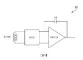
圖1係一MRI系統100之典型組件之一方塊圖。在圖1之說明性實例中,MRI系統100包括運算裝置104、控制器106、脈衝序列儲存裝置108、電力管理系統110及磁性組件120。應瞭解,系統100係說明性的且除或替代圖1中所圖解說明之組件,一MRI系統還可具有任何適合類型之一或多個其他組件。然而,一MRI系統通常將包含此等高階組件,儘管用於一特定MRI系統之此等組件之實施方案可相當不同,如下文進一步詳細論述。FIG. 1 is a block diagram of typical components of an
如圖1中所圖解說明,磁性組件120包括B0磁體122、勻場線圈124、RF傳輸及接收線圈126及梯度線圈128。磁體122可用於產生主磁場B0。磁體122可係可產生一所期望主磁場B0之磁性組件之任何適合類型或組合。如上文所論述,在高場型態中,通常使用一般而言以一螺線管幾何結構提供之超導材料形成B0磁體,從而需要低溫冷卻系統以使B0磁體保持在一超導狀態中。因此,高場B0磁體係昂貴、複雜的且消耗大量電力(例如,低溫冷卻系統需要顯著電力以維持使B0磁體保持在一超導狀態中所需之極低溫度),需要大的專用空間及專門化專用電力連接(例如,至電力網之一專用三相電力連接)。習用低場B0磁體(例如,在0.2 T下操作之B0磁體)亦通常使用超導材料來實施且因此具有此等相同一般要求。其他習用低場B0磁體使用永久磁體來實施,永久磁體產生習用低場系統所限制之場強度(例如,歸因於不能夠在較低場強度下獲取有用影像而介於0.2 T與0.3 T之間),需要重量在5噸至20噸之極大磁體。因此,習用MRI系統之B0磁體單獨妨礙可攜性及可負擔性兩者。As illustrated in FIG. 1, the
梯度線圈128可經配置以提供梯度場,且舉例而言可經配置以在三個大致正交方向(X、Y、Z)上於B0場中產生梯度。梯度線圈128可經組態以藉由使B0場(由磁體122及/或勻場線圈124產生之B0場)系統地變化來編碼所發射MR信號以將所接收MR信號之空間位置編碼為頻率或相位之一函數。舉例而言,梯度線圈128可經組態以使頻率或相位作為沿著一特定方向之空間位置之一線性函數而變化,儘管亦可藉由使用非線性梯度線圈來提供更複雜的空間編碼規範。舉例而言,一第一梯度線圈可經組態以使B0場在一第一(X)方向上選擇性地變化以在彼方向上執行頻率編碼,一第二梯度線圈可經組態以使B0場在大致正交於第一方向之一第二(Y)方向上選擇性地變化以執行相位編碼,且一第三梯度線圈可經組態以使B0場在大致正交於第一及第二方向之一第三(Z)方向上選擇性地變化以達成用於容積成像應用之切片選擇。如上文所論述,習用梯度線圈亦消耗通常由大的、昂貴梯度電源操作之顯著電力,如下文進一步詳細論述。The
藉由分別使用傳輸及接收線圈(通常稱為射頻(RF)線圈)激勵及偵測所發射MR信號來執行MRI。傳輸/接收線圈可包含用於傳輸及接收之單獨線圈、用於傳輸及/或接收之多個線圈或者用於傳輸及接收之相同線圈。因此,一傳輸/接收組件可包含用於傳輸之一或多個線圈、用於接收之一或多個線圈及/或用於傳輸及接收之一或多個線圈。傳輸/接收線圈通常亦可稱為Tx/Rx或Tx/Rx線圈以一般地指代用於一MRI系統之傳輸及接收磁性組件之各種組態。可在本文中互換地使用彼等術語。在圖1中,RF傳輸及接收線圈126包括一或多個傳輸線圈,其等可用於產生RF脈衝以誘發一振盪磁場B1。傳輸線圈可經組態以產生任何適合類型之RF脈衝。MRI is performed by separately using transmission and reception coils (commonly referred to as radio frequency (RF) coils) to stimulate and detect the transmitted MR signals. The transmission/reception coils may include separate coils for transmission and reception, multiple coils for transmission and/or reception, or the same coils for transmission and reception. Thus, a transmission/reception component may include one or more coils for transmission, one or more coils for reception, and/or one or more coils for transmission and reception. The transmission/reception coil is also commonly referred to as a Tx/Rx or Tx/Rx coil to generally refer to various configurations of transmission and reception magnetic components for an MRI system. These terms may be used interchangeably herein. In FIG. 1, the RF transmission and
電力管理系統110包含將操作電力提供至低場MRI系統100之一或多個組件之電子裝置。舉例而言,如下文更詳細論述,電力管理系統110可包含一或多個電力供應器、梯度電力組件、傳輸線圈組件及/或提供適合操作電力以使MRI系統100之組件通電及操作所需之任何其他適合電力電子裝置。如圖1中所圖解說明,電力管理系統110包括電力供應器112、電力組件114、傳輸/接收開關116及熱管理組件118 (例如,用於超導磁體之低溫冷卻設備)。電力供應器112包含將操作電力提供至MRI系統100之磁性組件120之電子裝置。舉例而言,電力供應器112可包含將操作電力提供至一或多個B0線圈(例如,B0磁體122)以產生用於低場MRI系統之主磁場之電子裝置。傳輸/接收開關116可用於選擇使RF傳輸線圈還是RF接收線圈操作。The
電力組件114可包含:一或多個RF接收(Rx)前置放大器,其等放大由一或多個RF接收線圈(例如,線圈126)偵測之MR信號;一或多個RF傳輸(Tx)電力組件,其等經組態以將電力提供至一或多個RF傳輸線圈(例如,線圈126);一或多個梯度電力組件,其等經組態以將電力提供至一或多個梯度線圈(例如,梯度線圈128);及一或多個勻場電力組件,其等經組態以將電力提供至一或多個勻場線圈(例如,勻場線圈124)。The
在習用MRI系統中,電力組件係大的、昂貴的且消耗顯著電力。通常,電力電子裝置佔用與MRI掃描器自身分離之一房間。電力電子裝置不僅需要空間,且亦係昂貴複雜裝置,其等消耗大量電力且需要支撐的壁裝式機架。因此,習用MRI系統之電力電子裝置亦妨礙MRI之可攜性及可負擔性。In conventional MRI systems, the power components are large, expensive, and consume significant power. Generally, power electronics occupies a room separate from the MRI scanner itself. Power electronic devices not only require space, but are also expensive and complicated devices, which consume large amounts of power and require wall-mounted racks. Therefore, the power electronic devices of conventional MRI systems also hinder the portability and affordability of MRI.
如圖1中所圖解說明,MRI系統100包含控制器106 (亦稱為一控制台),其具有控制電子裝置以將指令發送至電力管理系統110且自其接收資訊。控制器106可經組態以實施一或多個脈衝序列,其等用於判定發送至電力管理系統110以便以一所期望序列操作磁性組件120之指令(例如,用於操作RF傳輸及接收線圈126之參數、用於操作梯度線圈128之參數等)。如圖1中所圖解說明,控制器106亦與經程式化以處理所接收MR資料之運算裝置104互動。舉例而言,運算裝置104可處理所接收MR資料以使用任何適合影像重構程序來產生一或多個MR影像。控制器106可將關於一或多個脈衝序列之資訊提供至運算裝置104以便藉由運算裝置處理資料。舉例而言,控制器106可將關於一或多個脈衝序列之資訊提供至運算裝置104且運算裝置可至少部分基於所提供資訊執行一影像重構程序。在習用MRI系統中,運算裝置104通常包含一或多個高效能工作站,其等經組態以相對快速地對MR資料執行運算上昂貴的處理。此等運算裝置自身係相對昂貴的設備。As illustrated in FIG. 1, the
如自前述內容應瞭解,當前可用臨床MRI系統(包含高場、中場及低場系統)係大的、昂貴的、固定的安裝,從而需要大量專用且經特殊設計空間以及專用電力連接。發明者已開發出係較低成本、較低功率及/或可攜式之低場(包含極低場) MRI系統,從而顯著增加MRI之可用性及適用性。根據某些實施例,提供一可攜式MRI系統,從而允許將一MRI系統攜帶至病患且在需要其之位置處利用。As should be understood from the foregoing, currently available clinical MRI systems (including high-field, mid-field, and low-field systems) are large, expensive, and fixed installations, requiring a large number of dedicated and specially designed spaces and dedicated electrical connections. The inventors have developed low-field (including very low-field) MRI systems that are lower cost, lower power, and/or portable, thereby significantly increasing the usability and applicability of MRI. According to some embodiments, a portable MRI system is provided, allowing an MRI system to be carried to a patient and utilized where needed.
如上文所論述,某些實施例包含係可攜式的一MRI系統,,從而允許將MRI裝置移動至需要其之位置(例如,急診及手術室、初級醫療辦公室、新生兒加護病房、專業部門、緊急及行動運輸車輛以及現場)。一可攜式MRI系統之開發面臨眾多挑戰,包含大小、重量、電力消耗及在相對不受控制之電磁雜訊環境中(例如,一經特殊屏蔽之房間外部)操作之能力。As discussed above, some embodiments include a portable MRI system, allowing the MRI device to be moved to a location where it is needed (eg, emergency and operating room, primary medical office, neonatal intensive care unit, professional department , Emergency and mobile vehicles and the scene). The development of a portable MRI system faces many challenges, including size, weight, power consumption, and the ability to operate in relatively uncontrolled electromagnetic noise environments (eg, outside a specially shielded room).
可攜性之一態樣涉及在多種位置及環境中操作MRI系統之能力。如上文所論述,當前可用臨床MRI掃描器需要位於經特殊屏蔽之房間中以允許裝置之正確操作且係促成當前可用臨床MRI掃描器之成本、可用性缺乏及不可攜性之緣由中之一者(在諸多緣由當中)。因此,為在一經特殊屏蔽之房間外部操作,且更特定而言,為允許一般而言可攜式、可推式或以其他方式可運輸式MRI,MRI系統必須能夠在各種雜訊環境中操作。發明者已開發出允許MRI系統在經特殊屏蔽之房間外部操作之雜訊抑制技術,以便促進可攜式/可運輸式MRI以及不需要經特殊屏蔽之房間之固定MRI設施兩者。儘管雜訊抑制技術允許在經特殊屏蔽之房間外部操作,但此等技術亦可用於在經屏蔽環境(舉例而言,較廉價、鬆散或特定屏蔽之環境)中執行雜訊抑制,且因此可與已裝配有有限屏蔽之一區域結合使用,此乃因該等態樣不限於此方面。One aspect of portability involves the ability to operate an MRI system in multiple locations and environments. As discussed above, currently available clinical MRI scanners need to be located in specially shielded rooms to allow correct operation of the device and contribute to one of the reasons for the cost, lack of availability, and unportability of currently available clinical MRI scanners ( Among many reasons). Therefore, in order to operate outside of a specially shielded room, and more specifically, to allow portable, pushable or otherwise transportable MRI in general, the MRI system must be able to operate in various noise environments . The inventors have developed noise suppression techniques that allow MRI systems to operate outside of specially shielded rooms in order to promote both portable/transportable MRI and fixed MRI facilities that do not require specially shielded rooms. Although noise suppression techniques allow operation outside specially shielded rooms, these techniques can also be used to perform noise suppression in shielded environments (e.g., cheaper, loose, or specifically shielded environments), and therefore can Used in conjunction with an area that has been equipped with limited shielding, because these aspects are not limited to this aspect.
可攜性之一其他態樣涉及MRI系統之電力消耗。亦如上文所論述,當前臨床MRI系統消耗大量電力(例如,在操作期間範圍自20 kW至40 kW之平均電力消耗),因此需要專用電力連接(例如,至電網之專用三相電力連接能夠遞送所需電力)。一專用電力連接之要求係在除專門裝配有適合電力連接之昂貴專用房間之外的各種位置中操作一MRI系統之一進一步障礙。發明者已開發出能夠使用市電操作之低功率MRI系統,諸如一標準壁式插座(例如,美國的120 V/20 A連接)或普通的大電器插座(例如,220-240 V/30 A),從而允許裝置在提供普通電源插座之任何地方操作。「插入壁中」之能力促進可攜式/可運輸式MRI以及固定MRI系統安裝兩者而無需諸如一個三相電力連接之專門、專用電力。One of the other aspects of portability relates to the power consumption of MRI systems. As also discussed above, current clinical MRI systems consume large amounts of power (eg, average power consumption ranging from 20 kW to 40 kW during operation) and therefore require dedicated power connections (eg, dedicated three-phase power connections to the power grid can deliver Electricity required). The requirement for a dedicated power connection is one of the further obstacles to operating an MRI system in various locations other than an expensive dedicated room specifically equipped for power connection. The inventor has developed a low-power MRI system that can be operated using commercial power, such as a standard wall outlet (for example, 120 V/20 A connection in the United States) or an ordinary large electrical outlet (for example, 220-240 V/30 A) , Thereby allowing the device to operate anywhere a common power outlet is provided. The ability to "insert into the wall" facilitates the installation of both portable/transportable MRI and fixed MRI systems without the need for specialized, dedicated power such as a three-phase power connection.
如上文所論述,根據本文中所闡述之技術設計之一可攜式MRI裝置包含RF傳輸及接收線圈126,其經組態以在一傳輸操作期間產生一B1磁場且在一接收操作期間自由一經成像物件產生之一MR信號收集通量。在轉換成MR影像之前放大及處理由RF接收線圈感測之信號。由RF接收線圈126記錄之信號之控制及處理中所涉及之電路在本文中被稱為「RF信號鏈」電路。發明者已認識到,用於習用高場MRI系統中之RF信號鏈電路之組件並不適合及/或並未最佳化以供在根據本文中所闡述之技術設計之一低場MRI系統中使用。為此,某些實施例係關於供在一可攜式低場MRI系統中使用之經改良RF信號鏈電路。As discussed above, one portable MRI device designed according to the techniques set forth herein includes an RF transmission and
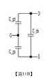
圖2示意性地圖解說明包含於某些實施例中之RF信號鏈電路200之某些組件。RF信號鏈電路200包含RF傳輸/接收線圈210及傳輸/接收電路212,傳輸/接收電路212經組態以取決於RF線圈210將操作以傳輸還是接收而將RF線圈210選擇性地耦合至RF接收電路。為最佳地操作,RF線圈通常經調諧以儘可能接近所謂拉莫(Larmor)頻率之一特定頻率而諧振。拉莫頻率(ω)係根據以下關係而與B0場之強度相關:
某些實施例包含多個RF線圈以改良由一RF線圈網路偵測之信號之信雜比(SNR)。舉例而言,RF線圈之一集合可配置於不同位置及定向處以偵測一綜合RF場。根據某些實施例,一可攜式MRI系統包括多個RF傳輸/接收線圈以改良影像獲取之SNR。舉例而言,一可攜式MRI系統可包括2個、4個、8個、16個、32個或更多個RF接收線圈以改良MR信號偵測之SNR。Some embodiments include multiple RF coils to improve the signal-to-noise ratio (SNR) of signals detected by an RF coil network. For example, a set of RF coils can be configured at different positions and orientations to detect an integrated RF field. According to some embodiments, a portable MRI system includes multiple RF transmit/receive coils to improve the SNR of image acquisition. For example, a portable MRI system may include 2, 4, 8, 16, 32 or more RF receiving coils to improve the SNR of MR signal detection.
如上文所論述,一般而言,RF線圈經調諧以在一所關注頻率(例如,拉莫頻率)下增加線圈敏感度。然而,毗鄰或相鄰線圈(例如,彼此充分接近之RF線圈)之間之電感耦合使經調諧線圈之敏感度降級且顯著減少RF線圈之集合之效用。存在用於幾何解耦相鄰線圈之技術但在空間上對線圈定向及位置施加了嚴格限制,從而減少了RF線圈之集合精確偵測RF場之能力,並因此使信雜比效能降級。As discussed above, in general, RF coils are tuned to increase coil sensitivity at a frequency of interest (eg, Lamo frequency). However, inductive coupling between adjacent or adjacent coils (eg, RF coils that are sufficiently close to each other) degrades the sensitivity of the tuned coils and significantly reduces the effectiveness of the set of RF coils. There are techniques for geometrically decoupling adjacent coils but place strict restrictions on the coil orientation and position in space, thereby reducing the ability of the set of RF coils to accurately detect the RF field, and thus degrading the signal-to-noise ratio performance.
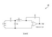
為解決線圈之間電感耦合之負面影響,發明者已利用減少多線圈傳輸/接收系統中射頻線圈之間電感耦合之效應之線圈解耦技術。舉例而言,圖3圖解說明一被動解耦電路300,其經組態以減少一多線圈傳輸/接收系統中射頻線圈之間之電感耦合。電路300經組態以解耦可經受B1傳輸場(例如,來自一RF傳輸線圈)之RF線圈。解耦電路之目的係最小化在拉莫頻率下針對一既定AC激勵電壓穿過RF線圈之電流。特定而言,電感器L1表示MRI系統之視場內之一RF信號線圈。電容器C1及C2形成一調諧電路,其將線圈之電感匹配至低雜訊放大器(LNA)之輸入以最佳化雜訊效能阻抗。電感器L2及電容器C3形成一槽電路,其減少在包含L1、C1及C2之迴路中流動之電流以防止RF線圈耦合至其他線圈。圖4A圖解說明基於圖3中之電路300之一模擬在RF線圈之諧振頻率下LNA輸入處之電壓之一曲線圖。圖4B圖解說明基於圖3中之電路300之一模擬穿過RF線圈之電流之一曲線圖。如所展示,在2.75 MHz之諧振頻率下,LNA電壓係約26 dB (圖4A)且線圈電流係-37 dB (圖4B)。在圖4A及圖4B中之每一者中,經量測量之量值表示為一實線且經量測量之相位表示為一虛線。To address the negative effects of inductive coupling between coils, the inventors have utilized coil decoupling techniques that reduce the effect of inductive coupling between radio frequency coils in multi-coil transmission/reception systems. For example, FIG. 3 illustrates a
發明者已認識到,使用一經調諧匹配濾波器解耦以減少RF線圈中之電流具有某些缺點,包含將多個組件(例如,電容器C1、C2及C3)調諧至線圈之操作頻率之需要。此外,電感器L2中之損失導致SNR之一損失。如此,解耦效率係與SNR效率之一折衷。此外,如圖4B中所展示,儘管經調諧匹配濾波器大致在諧振頻率下減少線圈電流,但電流波形中之尖銳波穀演示,穿過RF線圈之電流減少僅針對圍繞諧振頻率之一有限頻寬係小的。The inventors have recognized that using a tuned matched filter to decouple to reduce current in the RF coil has certain disadvantages, including the need to tune multiple components (eg, capacitors C1, C2, and C3) to the operating frequency of the coil. In addition, the loss in inductor L2 causes one of the SNR losses. As such, decoupling efficiency is a compromise between SNR efficiency. In addition, as shown in FIG. 4B, although the tuned matched filter substantially reduces the coil current at the resonant frequency, the sharp valleys in the current waveform demonstrate that the current reduction through the RF coil is only for a limited frequency around one of the resonant frequencies The width is small.
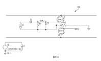
某些實施例係關於一經改良解耦電路,其經組態以藉由使用來自放大器之輸出之回饋而阻尼線圈回應來減少RF線圈中之電流。圖5展示根據某些實施例經組態以提供回饋解耦之一解耦電路400之一實例。電路400包含自一放大器LNA之輸出至LNA之一輸入之一主動回饋路徑。在圖5中所展示之實例中,主動回饋路徑包含一單個回饋路徑。然而,應瞭解,另一選擇係,主動回饋路徑可實施為複數個回饋路徑,其每一者在被選擇時提供一不同類型之回饋解耦。舉例而言,在某些實施例中,主動回饋路徑包含:一第一回饋路徑,其經組態以提供一第一回饋信號;及一第二回饋路徑,其經組態以提供一第二回饋信號。Certain embodiments are related to an improved decoupling circuit that is configured to reduce the current in the RF coil by using the feedback from the output of the amplifier to damp the coil response. FIG. 5 shows an example of a
發明者已認識到,回饋信號之相位影響在調諧頻率下之放大增益。舉例而言,在於主動回饋路徑中包含多個回饋路徑之某些實施例中,一第一回饋路徑可提供與RF線圈之一諧振頻率異相90度或270度之一第一回饋信號,且一第二回饋路徑可提供與RF線圈之一諧振頻率異相180度之一第二回饋信號。另一選擇係,放大器之增益可調諧成與線圈之諧振頻率異相90度或270度。當使用270度之一相位時,調諧頻率下之放大增益可係最大的。在其中使用一單個回饋路徑之其他實施例中,可將回饋信號之相位設定為180度以歸因於線圈中之較少電流而提供更高效解耦。The inventor has recognized that the phase of the feedback signal affects the amplification gain at the tuned frequency. For example, in some embodiments where the active feedback path includes multiple feedback paths, a first feedback path may provide a first feedback signal that is 90 degrees or 270 degrees out of phase with a resonant frequency of the RF coil, and a The second feedback path may provide a second feedback signal 180 degrees out of phase with a resonance frequency of one of the RF coils. Alternatively, the gain of the amplifier can be tuned to be 90 degrees or 270 degrees out of phase with the resonant frequency of the coil. When a phase of 270 degrees is used, the amplification gain at the tuning frequency can be the largest. In other embodiments where a single feedback path is used, the phase of the feedback signal can be set to 180 degrees to provide more efficient decoupling due to less current in the coil.
由電路400提供之回饋解耦使用主動負回饋以阻尼線圈回應(亦稱為減少線圈之品質(Q)因子或「de-Qing」線圈)且藉此減少RF線圈中流動之電流。如所展示,電路400亦包含一調諧/匹配電路,其配置於RF線圈與LNA之間。可根據某些實施例使用任何適合調諧/匹配電路,其實例在下文中闡述。The feedback decoupling provided by the
圖6圖解說明使用一單個電容器C1實施調諧/匹配電路之一基於回饋之解耦電路500。與解耦電路300相比,解耦電路500僅包含一單個組件(亦即,電容器C1)用以調諧。此外,由於電路500僅包含電抗組件C1及C2且在調諧/匹配電路中不包含一電感器,因此該解耦電路不會歸因於在電路300中包含電感器L1而引入與電路300相關聯的SNR損失。FIG. 6 illustrates a feedback-based
可使用具有一固定值之一電容器來實施電容器C1。另一選擇係,可使用具有一可變值之一電容器(例如,一變容二極體)來實施電容器C1。在仍其他實施例中,可使用與具有可變值之一電容器並聯配置的具有固定值(例如,300 pF)之一電容器來實施電容器C1。此一配置減少藉由在回饋迴路中使用一可變電容器而引入之AC損失之效應。The capacitor C1 may be implemented using a capacitor having a fixed value. Alternatively, a capacitor C1 may be implemented using a capacitor with a variable value (for example, a varactor diode). In still other embodiments, capacitor C1 may be implemented using a capacitor having a fixed value (eg, 300 pF) configured in parallel with a capacitor having a variable value. This configuration reduces the effect of AC losses introduced by using a variable capacitor in the feedback loop.
圖7A圖解說明基於圖5中之電路500之一模擬在RF線圈之諧振頻率下LNA輸入處之電壓之一曲線圖。圖7B圖解說明基於圖6中電路500之一模擬穿過RF線圈之電流之一曲線圖。如所展示,在2.75 MHz之諧振頻率下,LNA輸入電壓係約8 dB (圖7A)且穿過線圈之電流係約-35 dB。然而,與在線圈之諧振頻率下展示一尖銳波穀之圖4B中所展示之線圈電流曲線圖相比,圖7B展示與電路300相比當使用解耦電路500時線圈電流在一更寬頻帶上減少。因此,與電路300相比,電路500提供一較寬頻帶上之RF線圈解耦。7A illustrates a graph of the voltage at the LNA input at the resonant frequency of the RF coil based on a simulation of one of the
圖8圖解說明一替代基於回饋之解耦電路600,其中圖6中所展示之電路500之單個電容器調諧/匹配電路被替換為包含組件C1、C3及L2之一調諧/匹配網路。在電路600中,除了具有由包含電容器C2之一主動回饋路徑提供之基於回饋之解耦之外,一調諧/匹配網路還可用於調諧RF線圈(表示為L1)。FIG. 8 illustrates an alternative feedback-based
在某些實施例中,舉例而言,分別由圖5、圖6及圖8中之電路400、500及600之回饋組件提供之電容式回饋電路被替換為互感回饋電路。圖24圖解說明一替代基於回饋之解耦電路2400,其中舉例而言,圖6之電路500中所展示之電容式回饋電路被替換為包含組件R1、R2及L2之互感回饋電路。在電路2400中,電感器L1及L2(例如)使用一變壓器或經由空氣相互耦合。In some embodiments, for example, the capacitive feedback circuits provided by the feedback components of the
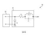
根據某些實施例用於提供RF線圈解耦之另一技術係在RF信號鏈中提供一傳輸/接收開關。傳輸/接收開關經組態以在RF信號正由一或多個RF傳輸線圈傳輸時將RF線圈與放大器隔離。具體而言,傳輸/接收開關將調諧/匹配網路劃分成兩個網路部分以在RF傳輸循環期間保護敏感電子裝置。在某些習用MRI系統(例如,高場MRI系統)中,通常使用一個二極體(諸如一PIN二極體)來實施傳輸/接收開關312。包含一個二極體D1之傳輸/接收開關電路之一實例在圖9中展示為電路700。在一傳輸脈衝期間,二極體D1經接通以形成一短路,從而將RF信號線圈與接收電子裝置隔離。如上文結合電路300所闡述,所得網路提供具有一高阻抗之一槽電路,其確保RF線圈中之電流保持為小。在接收循環期間,二極體D1被關閉,從而導致RF線圈被連接至放大器且由槽電路調諧,該槽電路經組態以限制穿過RF線圈之電流,同時允許在放大器之輸出處偵測到充足信號。因此,RF線圈在傳輸循環期間被連接至一第一槽電路且在一脈衝序列之接收循環期間被連接至一第二槽電路。Another technique for providing RF coil decoupling according to certain embodiments is to provide a transmit/receive switch in the RF signal chain. The transmit/receive switch is configured to isolate the RF coil from the amplifier when the RF signal is being transmitted by one or more RF transmit coils. Specifically, the transmit/receive switch divides the tuning/matching network into two network parts to protect sensitive electronic devices during the RF transmission cycle. In some conventional MRI systems (eg, high-field MRI systems), a diode (such as a PIN diode) is usually used to implement the transmit/receive
習用解耦電路(諸如圖9中所展示之彼電路)通常使用PIN二極體來將接收電子裝置與RF信號線圈隔離。然而,適合於在一解耦電路中執行此功能之PIN二極體需要大約0.1 A之電流以接通二極體。作為一實例,具有八個接收線圈之一傳輸/接收線圈系統可需要大約0.8 A之電流以針對一影像獲取脈衝序列之每一傳輸及接收循環將接收線圈與RF信號線圈解耦。因此,在一影像獲取協定之時段內,RF傳輸/接收系統之解耦電路消耗大量電力。此外,當使用PIN二極體時,需要一加偏壓電阻器R1及包含組件L1及C1之一AC阻斷濾波器,且當二極體係在關閉狀態中時不隔離電路之接地。此外,儘管PIN二極體在用於高場MRI系統中之較高頻率下工作良好,但PIN二極體在用於低場或極低場MRI系統中之低操作頻率(例如,小於10 MHz)下工作不良。在此等低頻率下,PIN二極體整流信號而非阻斷信號。舉例而言,一DC偏壓電流Ibias允許甚至在施加一負信號時加正向偏壓於二極體。對於頻率f及峰值電流Ipeak之一AC信號,根據以下關係:τIbias>Ipeak/f,比率Ipeak/f需要低於DC偏壓電流Ibias與載子壽命τ之乘積,以使PIN二極體適當地起作用以阻斷信號。然而,某些低場MRI應用可具有以下參數:Ipeak= 10A、f= 2.75 MHz、Ibias= 100 mA。根據以上關係,對於此等參數,PIN二極體將需要具有一載子壽命τ > 37 μs,此並非商用PIN二極體之一特性。Conventional decoupling circuits (such as the other circuit shown in FIG. 9) typically use PIN diodes to isolate the receiving electronics from the RF signal coil. However, a PIN diode suitable for performing this function in a decoupling circuit requires a current of about 0.1 A to turn on the diode. As an example, a transmission/reception coil system with one of the eight reception coils may require a current of about 0.8 A to decouple the reception coil from the RF signal coil for each transmission and reception cycle of an image acquisition pulse sequence. Therefore, the decoupling circuit of the RF transmission/reception system consumes a lot of power during an image acquisition agreement period. In addition, when using a PIN diode, a biasing resistor R1 and an AC blocking filter including components L1 and C1 are required, and the ground of the circuit is not isolated when the diode system is in the off state. In addition, although PIN diodes work well at higher frequencies used in high-field MRI systems, PIN diodes operate at low frequencies in low-field or very low-field MRI systems (eg, less than 10 MHz ) Under bad work. At these low frequencies, the PIN diode rectifies the signal instead of blocking it. For example, a DC bias currentIbias allows a positive bias to be applied to the diode even when a negative signal is applied. For an AC signal of frequencyf and peak currentIpeak , according to the following relationship: τIbias >Ipeak /f , the ratioIpeak /f needs to be lower than the product of the DC bias currentIbias and the carrier lifetime τ, so that The PIN diode functions properly to block the signal. However, some low-field MRI applications may have the following parameters:Ipeak = 10A,f = 2.75 MHz,Ibias = 100 mA. According to the above relationship, for these parameters, the PIN diode will need to have a carrier lifetime τ> 37 μs, which is not one of the characteristics of commercial PIN diodes.
發明者已認識到,通常用於一解耦電路中之PIN二極體可由氮化鎵(GaN)場效應電晶體(FET)替換以解決在一低場MRI系統之一RF傳輸/接收電路中使用PIN二極體之缺點中之某些缺點,包含減少RF傳輸/接收系統之電力消耗。特定而言,GaN FET需要大約數個微安培來接通,從而將電力消耗減少數個數量級。此外,與PIN二極體相比,GaN FET之電阻在接通時係小的,從而減少對槽電路之負面影響。根據某些實施例,電路700中之二極體D1被替換為一或多個GaN FET,藉此減少RF傳輸/接收系統之電力消耗。The inventors have realized that the PIN diodes commonly used in a decoupling circuit can be replaced by gallium nitride (GaN) field effect transistors (FET) to solve in one of the RF transmission/reception circuits of a low field MRI system Some of the disadvantages of using PIN diodes include reducing the power consumption of RF transmission/reception systems. In particular, GaN FETs require approximately a few microamperes to turn on, thereby reducing power consumption by orders of magnitude. In addition, compared to PIN diodes, the resistance of GaN FETs is small when turned on, thereby reducing the negative impact on the tank circuit. According to some embodiments, the diode D1 in the
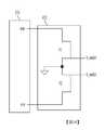
圖10圖解說明根據某些實施例之一RF傳輸/接收開關電路412,其中電路700之二極體D1已替換為一對鏡像FET (例如,GaN FET) F1及F2。儘管電路412包含一對鏡像FET,但在某些實施例中,一RF傳輸/接收開關電路412可包含任何適合數目個FET,包含但不限於一單個FET。不同於PIN二極體,GaN FET在所有頻率下操作良好,具有可忽略之電力消耗,在關閉狀態中接地隔離,並具有較PIN二極體低之一接通狀態電阻(例如,<0.1 Ohm)。FIG. 10 illustrates one of the RF transmission/
圖11A至圖11C圖解說明根據某些實施例之一FET在一RF傳輸/接收系統中用作一開關之操作狀態。圖11A圖解說明一GaN FET,其組態為一汲極節點D與一源極節點S之間之一開關。GaN FET之閘極G用於控制開關在接通與關閉之間之狀態。圖11B圖解說明在關閉狀態中GaN FET可藉助三個經集總電容器C_ds、C_gs及C_gd模型化。在此一組態中,在C_ds之值係小的(例如,10-100 pF)之情形中,汲極D係與源極S隔離。在某些實施例中,包含於一傳輸/接收開關中之至少一個GaN FET之汲極-源極電容係至少15 pF。圖11C圖解說明在接通狀態中,汲極-源極電容C_ds由一短路替換。11A to 11C illustrate an operation state in which an FET is used as a switch in an RF transmission/reception system according to some embodiments. FIG. 11A illustrates a GaN FET configured as a switch between a drain node D and a source node S. FIG. The gate G of the GaN FET is used to control the state of the switch between on and off. FIG. 11B illustrates that the GaN FET can be modeled with three lumped capacitors C_ds, C_gs, and C_gd in the off state. In this configuration, in the case where the value of C_ds is small (for example, 10-100 pF), the drain D is isolated from the source S. In some embodiments, the drain-source capacitance of at least one GaN FET included in a transmit/receive switch is at least 15 pF. FIG. 11C illustrates that in the on state, the drain-source capacitance C_ds is replaced by a short circuit.
圖12圖解說明根據某些實施例用於在經配置以作為一RF傳輸/接收開關操作之GaN FET U1及U2上驅動一閘極電壓之一電路1000。GaN FET經組態以將接收電子裝置與RF線圈耦合及解耦。如所展示,電感器L5及L6被配置為經組態以將一控制信號V2耦合至FET U1及U2之閘極之一變壓器,同時提供接地隔離。二極體D3操作以整流控制信號以跨越電容器C7於閘極處形成一DC開/關電壓。電阻器R11經組態以使電容器C7及FET之閘極電容放電。R11及C7+Cgates之時間常數判定傳輸/接收開關關閉得多快。在某些實施例中,控制信號V2可係耦合至電感器L5之一10 MHz正弦波以驅動FET。在操作中,可接通/關閉10 MHz信號以使FET閘極充電且接著關閉。然後電阻器R11使閘極驅動器放電以斷開開關。在圖12之實例中,電感器L5與L6之間之耦合可係不良的且電感係小的。舉例而言,在某些實施例中,L5/L6可實施為小的空心變壓器或一RF變壓器。FIG. 12 illustrates a
圖13圖解說明根據某些實施例用於在經配置以作為一RF傳輸/接收開關操作之GaN FET U1及U2上驅動一閘極電壓之一驅動電路1100。在電路1100中,除使用一外部提供之控制信號V2 (如在電路1000中)外,將RF傳輸脈衝自身用作控制信號以閘控傳輸/接收開關。在圖13之實例中,由電感器L6表示之一線圈經組態以接收RF傳輸脈衝,且作為回應,產生驅動GaN FET之閘極之一電壓。在某些實施例中,一RF線圈陣列中之RF線圈中之每一者可與一線圈L6相關聯,線圈L6經組態以接收用於彼線圈之RF傳輸脈衝。在其他實施例中,一多線圈陣列中之RF線圈中之一子集(例如,一者)可與經組態以接收RF傳輸脈衝之線圈L6相關聯,且可將由線圈L6回應於接收到傳輸脈衝而產生之開關信號散佈至與陣列中之其他RF線圈相關聯之電路。與電路1000相比,電路1100使用較不複雜之驅動電路,此乃因不需要一單獨控制信號產生器。然而,將傳輸脈衝用作一控制信號之一結果係開關並不閉合直至在RF傳輸開始之稍後且RF傳輸脈衝可由脈衝接收器線圈L6偵測到。13 illustrates a
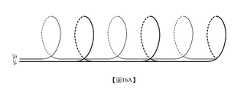
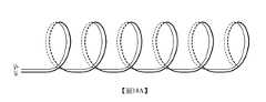
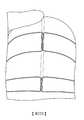
某些實施例係關於用於供在一低場MRI系統中使用之一射頻(RF)線圈之一新穎設計。供在MRI系統中使用之某些習用RF線圈設計被組態為一螺線管,其以一螺旋型樣纏繞在一待成像物件上。舉例而言,通常用於MRI系統中之頭部線圈包含形成於一螺線管組態中之一導體,使得一人之一頭部可插入螺線管之內部。圖14A示意性地圖解說明一螺線管RF線圈設計,其中一導體係在一單個遍次中以複數個廻圈自一基板之一第一側至與第一側相對之基板之一第二側纏繞在該基板上。當到達基板之第二側時,導體可返回至第一側而不形成額外廻圈,如所展示。圖14B展示圖14A之線圈配置之一俯視圖,其中導體之廻圈由垂直線表示。點V+及V-表示線圈中之導體之端,該等端在一MRI系統中被連接至經組態以放大所記錄信號之一放大器(例如,一低雜訊放大器)。Certain embodiments are related to a novel design for a radio frequency (RF) coil for use in a low field MRI system. Some conventional RF coil designs for use in MRI systems are configured as a solenoid, which is wound on an object to be imaged in a spiral pattern. For example, the head coil commonly used in MRI systems includes a conductor formed in a solenoid configuration so that one head of a person can be inserted into the solenoid. FIG. 14A schematically illustrates a solenoid RF coil design, in which a guide system has a plurality of turns from a first side of a substrate to a second side of a substrate opposite to the first side in a single pass Side wrapped around the substrate. When reaching the second side of the substrate, the conductor can return to the first side without forming additional loops, as shown. 14B shows a top view of the coil configuration of FIG. 14A, where the loop of the conductor is represented by a vertical line. Points V+ and V- represent the ends of the conductors in the coil, which are connected to an amplifier (eg, a low noise amplifier) configured to amplify the recorded signal in an MRI system.
在一理想情形中,在RF線圈之輸出處記錄之電位經平衡使得在線圈中缺乏電動勢(emf)之情形下V+ - V- = 0。然而,當一物件(諸如一人之頭部)插入至螺線管線圈中時,寄生耦合發生於物件與線圈中之導體之間,此可導致V+及V-不平衡且在放大器輸入處產生一電壓。當線圈用於MRI系統中時,電壓顯示為所記錄MR信號中之一雜訊信號。取決於頭部在RF線圈內之位置,寄生耦合可不同地影響在點V+及V-處記錄之信號。舉例而言,當物件插入在線圈之一端處時,歸因於寄生耦合而引入至所記錄信號中之雜訊之量值在點V+處與點V-相比可係大的,此乃因V+與雜訊被引入至線圈中之點之間之較短導體距離。另一選擇係,若物件配置於點V+與V-之間之線圈之中心處或附近,則引入至線圈中之雜訊將同等地影響在點V+及V-兩者處所偵測之電壓。在仍另一實施方案中,若物件配置成較靠近點V-,則較點V+將在點V-處偵測更多雜訊,從而導致一不平衡輸出(亦即,V+ - V- ≠ 0)。In an ideal situation, the potential recorded at the output of the RF coil is balanced such that in the absence of an electromotive force (emf) in the coil, V+-V- = 0. However, when an object (such as a person's head) is inserted into the solenoid coil, parasitic coupling occurs between the object and the conductor in the coil, which can cause V+ and V- imbalance and produce a Voltage. When the coil is used in an MRI system, the voltage is displayed as one of the noise signals of the recorded MR signals. Depending on the position of the head within the RF coil, parasitic coupling may affect the signals recorded at points V+ and V- differently. For example, when an object is inserted at one end of the coil, the magnitude of the noise introduced into the recorded signal due to parasitic coupling at point V+ may be larger than point V-, because The short conductor distance between V+ and the point where noise is introduced into the coil. Another option is that if the object is placed at or near the center of the coil between points V+ and V-, the noise introduced into the coil will equally affect the voltage detected at both points V+ and V-. In yet another embodiment, if the object is configured closer to point V-, then more noise will be detected at point V- than point V+, resulting in an unbalanced output (i.e., V+-V- ≠ 0).
圖15A示意性地圖解說明當一物件(表示為電壓源V0)在一特定位置處插入至一螺線管線圈中時,一寄生耦合(表示為阻抗ZC)在線圈中之一單個點處被引入至線圈中。應瞭解,實務上,將散佈自物件至線圈繞組之寄生耦合。圖15B圖解說明寄生耦合之引入如何影響在導體之端處量測之電壓V+、V-之一阻抗模型。ZC表示物件與線圈之間之寄生耦合,Z+表示引入寄生耦合之點與點V+之間之導體中之阻抗,Z-表示引入寄生耦合之點與點V-之間之導體中之阻抗,且ZG表示導體之端中之每一者(亦即,V+及V-)與接地之間之阻抗。當物件與線圈之間存在一弱寄生耦合(例如,ZC˃˃ Z+、Z-、ZG)時,以下關係闡述導體V+及V-之兩個端處電位之不同:
由於V+及V-處之線圈之輸出可係不平衡的,某些習用RF線圈包含RF線圈與放大器之間之一平衡-不平衡變壓器以提供一平衡輸出且拒斥引入至線圈中之共模雜訊。發明者已認識到,不期望在一低場MRI系統中使用平衡-不平衡變壓器來拒斥引入至一RF線圈中之共模雜訊,此歸因於由線圈接收之小量值信號及平衡-不平衡變壓器之有損特性。為此,某些實施例係關於一RF線圈設計,其使用經設計以減少共模雜訊之一纏繞型樣,此減輕使用一平衡-不平衡變壓器之需要。Since the output of the coils at V+ and V- can be unbalanced, some conventional RF coils include a balance-unbalance transformer between the RF coil and the amplifier to provide a balanced output and reject the common mode introduced into the coil Noise. The inventors have realized that it is undesirable to use a balun transformer in a low-field MRI system to reject common-mode noise introduced into an RF coil due to the small amount of signal received by the coil and balance -Lossy characteristics of unbalanced transformers. For this reason, some embodiments relate to an RF coil design that uses a winding pattern designed to reduce common mode noise, which alleviates the need to use a balun.
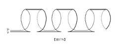
圖16至圖19示意性地圖解說明根據某些實施例之RF線圈設計。對於圖16至圖19中所展示之線圈設計,結果係一螺線管線圈具有與圖14A中所展示之習用線圈纏繞型樣類似之磁性質。舉例而言,位於彼此附近之線圈之匝偵測一類似磁通量。然而,圖16至圖19中所展示之RF線圈之電性質不同於用於圖14A線圈設計之彼等電性質。特定而言,圖16至圖19中所展示之纏繞設計在一待成像物件插入線圈中時導致經改良平衡及共模拒斥。如所展示,當一待成像物件插入至一線圈中時,物件與導體之間之寄生耦合導致在位於物件附件之導體之匝中誘發一電壓。對於圖16至圖19中所展示之纏繞型樣,當將一電壓施加至導體時,導體之毗鄰匝具有一類似電感及電位,此乃因毗鄰匝位於距各別點V+及V-之一類似距離。因此,歸因於插入線圈中之一物件至導體之寄生耦合而在導體中誘發之電壓顯示為於輸出V+及V-兩者處類似之一雜訊信號 - 而不管物件在線圈中之位置,使得V+ - V- ~ 0,藉此減少共模雜訊。16 to 19 schematically illustrate RF coil designs according to certain embodiments. For the coil designs shown in FIGS. 16-19, the result is that a solenoid coil has magnetic properties similar to the conventional coil winding pattern shown in FIG. 14A. For example, the turns of coils located near each other detect a similar magnetic flux. However, the electrical properties of the RF coils shown in FIGS. 16-19 are different from those of the coil design used in FIG. 14A. In particular, the winding design shown in FIGS. 16-19 results in improved balance and common mode rejection when an object to be imaged is inserted into the coil. As shown, when an object to be imaged is inserted into a coil, the parasitic coupling between the object and the conductor causes a voltage to be induced in the turns of the conductor located at the attachment of the object. For the winding patterns shown in FIGS. 16 to 19, when a voltage is applied to the conductor, the adjacent turns of the conductor have a similar inductance and potential because the adjacent turns are located at one of the respective points V+ and V- Similar distance. Therefore, the voltage induced in the conductor due to the parasitic coupling of an object inserted into the coil to the conductor appears to be a noise signal similar at both the output V+ and V--regardless of the position of the object in the coil, Make V+-V- ~ 0, thereby reducing common mode noise.
除如圖14A中所展示在一單個廻圈遍次中自RF之一端至另一端纏繞導體外,在某些實施例中,以一平衡型樣使用多個(例如,兩個)廻圈或部分廻圈遍次自端至端地纏繞導體。圖16A展示一「交錯」纏繞型樣,其中在一基板之一端處開始之一導體係藉由在一第一遍次中沿著纏繞方向與導體之一第一端間隔開之不同層級處跳過基板之部分而纏繞在基板上。當導體在一第二遍次中自基板之另一(第二)端纏繞時,導體纏繞在於第一遍次中跳過之基板之彼等部分上。圖16B展示圖16A中所圖解說明之交錯纏繞型樣之一俯視圖。In addition to winding the conductor from one end to the other end of RF in a single loop pass as shown in FIG. 14A, in certain embodiments, multiple (eg, two) loops or Partial loops wrap the conductor from end to end. Figure 16A shows a "staggered" winding pattern in which a conductive system starting at one end of a substrate jumps at different levels spaced from the first end of a conductor along the winding direction in a first pass It is wound on the substrate through the part of the substrate. When the conductor is wound from the other (second) end of the substrate in the second pass, the conductor is wound on the other parts of the substrate skipped in the first pass. 16B shows a top view of one of the intertwined patterns illustrated in FIG. 16A.
圖16A中所展示之交錯纏繞型樣在一第一遍次中跳過完整匝(例如,360°轉數)且在相反方向上於第二遍次中填充於彼等所跳過匝中。然而,應瞭解,亦預期替代交錯纏繞型樣。舉例而言,圖17A展示一交錯型樣,其中除在第一遍次中跳過一完整匝(例如,360°)外,纏繞型樣還在複數個層級中之每一者處自基板之第一端圍繞基板完成一系列半匝(例如,180°),同時跳過第一遍次中該等匝之另一半。然後在第二遍次期間自基板之第二端至第一端填充經跳過半匝,從而導致一完全螺線管線圈組態。圖17B展示圖17A之半匝跳過交錯纏繞設計之一俯視圖。下文中所更詳細闡述之圖22A至圖22L圖解說明用於實施圖17A中所圖解說明之半匝跳過設計之一程序。The interleaved winding pattern shown in FIG. 16A skips a complete turn (eg, 360° revolutions) in a first pass and fills in the skipped turns in the second pass in the opposite direction. However, it should be understood that alternative winding patterns are also expected. For example, FIG. 17A shows a staggered pattern in which, in addition to skipping a complete turn (eg, 360°) in the first pass, the winding pattern is also removed from the substrate at each of the multiple levels The first end completes a series of half turns (eg, 180°) around the substrate while skipping the other half of the turns in the first pass. Then during the second pass, the half-turn is filled from the second end to the first end of the substrate, resulting in a complete solenoid coil configuration. 17B shows a top view of the half-turn skip staggered winding design of FIG. 17A. FIGS. 22A to 22L, explained in more detail below, illustrate one procedure for implementing the half-turn skip design illustrated in FIG. 17A.
圖18A圖解說明根據某些實施例之一替代平衡纏繞型樣之一實例。在圖18A中所展示之纏繞型樣中,第一複數個導體廻圈自第一端至第二端纏繞在基板上,而不跳過第一遍次上之任何層級。在自第二端至第一端之第二遍次上,位於第一複數個廻圈附近之第二複數個廻圈纏繞在基板上以形成一「雙」纏繞型樣。圖18B展示圖18A中所圖解說明之纏繞型樣之一俯視圖。FIG. 18A illustrates an example of an alternative balanced winding pattern according to one of certain embodiments. In the winding pattern shown in FIG. 18A, the first plurality of conductor loops are wound on the substrate from the first end to the second end without skipping any level on the first pass. On the second pass from the second end to the first end, the second plural loops located near the first plural loops are wound on the substrate to form a "double" winding pattern. 18B shows a top view of one of the winding patterns illustrated in FIG. 18A.
圖19展示根據某些實施例具有一交錯組態之另一平衡纏繞型樣之一俯視圖。在圖19中所展示之纏繞型樣中,除自基板之一第一端至基板之一第二端在一系列層級中形成廻圈外(例如,如圖16A中所展示),導體在一第一遍次中自基板之第一端至第二端纏繞成一螺旋組態,且在一第二遍次中自基板之第二端至第一端纏繞成一逆螺旋組態。形成螺旋纏繞組態之特定角度並非對本發明之實施例之一限制,此乃因可使用針對圍繞基板之任何所期望數目個匝之任何適合角度。19 shows a top view of another balanced winding pattern with a staggered configuration according to some embodiments. In the winding pattern shown in FIG. 19, except that a loop is formed in a series of levels from a first end of the substrate to a second end of the substrate (for example, as shown in FIG. 16A), the conductor is in a In the first pass, a spiral configuration is wound from the first end to the second end of the substrate, and in a second pass, a reverse spiral configuration is wound from the second end to the first end of the substrate. The particular angle forming the spiral wound configuration is not a limitation of one embodiment of the invention, as any suitable angle for any desired number of turns around the substrate can be used.
上文結合圖16至圖19所闡述之平衡纏繞型樣係關於具有一螺線管組態之RF線圈,其中一物件(例如,一病患之頭部)插入螺線管內。發明者已認識到,本文中所闡述之平衡纏繞技術亦可用於除一螺線管線圈之外的線圈組態。舉例而言,圖20圖解說明使用一平衡纏繞型樣來形成一RF表面線圈之一實例。表面線圈包含配置成彼此緊鄰的兩個導體繞組。如所展示,可使兩個繞組之間之距離(h)為小(例如,接近幾乎等於0的一距離),使得多個繞組具有類似於具有一單個繞組之一線圈之磁性質。在某些實施例中,兩個繞組可組態成彼此異相180°。The balanced winding pattern described above in connection with FIGS. 16 to 19 relates to an RF coil having a solenoid configuration in which an object (for example, a patient’s head) is inserted into the solenoid. The inventor has realized that the balanced winding technique described herein can also be used for coil configurations other than a solenoid coil. For example, FIG. 20 illustrates an example of using a balanced winding pattern to form an RF surface coil. The surface coil includes two conductor windings arranged in close proximity to each other. As shown, the distance (h) between the two windings can be made small (eg, close to a distance nearly equal to 0), so that the multiple windings have magnetic properties similar to one of the coils with a single winding. In some embodiments, the two windings may be configured 180° out of phase with each other.
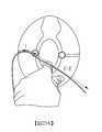
圖21圖解說明根據某些實施例用於製造一RF線圈之一程序2100。在動作2110中,提供一基板,一導體將纏繞在該基板上。該基板可由任何適合非磁性材料製成。在某些實施例中,該基板包括(舉例而言)使用一加性製造程序(例如,3D印刷)製作之一塑膠材料。然後程序2130進行至動作2112,其中複數個槽形成於基板中。舉例而言,該基板可包含一頂部及一底部且複數個槽可形成於自基板之頂部至基板之底部間隔開之位置處。在某些實施例中,基板形成一頭盔之形狀,一人之頭部可放置在該頭盔內,且該等槽自頂部至底部圍繞頭盔之一圓周形成為複數個圓周槽或「環」。在某些實施例中,自基板之頂部至底部使用一相同間距來分離複數個環以形成其內可纏繞一導體之複數個層級。複數個槽亦可包含連接圓周槽之複數個連接槽。在某些實施例中,該等槽可作為製作基板之部分而形成於基板中(例如,使用一加性製造程序),使得不需要在基板中形成槽之一單獨動作。FIG. 21 illustrates a
然後程序2100進行至動作2114,其中一導體之一第一部分纏繞於形成於基板中之槽之一第一部分內。如上文結合圖17A所論述,在某些實施例中,導體之一第一部分可藉由跳過每一其他層級自基板之頂部至底部纏繞於位於交替層級處之槽中。在其他實施例中,導體之一第一部分可在每一層級上纏繞於槽之部分(例如,半匝)內,同時在每一層級上跳過槽之其他部分。然後程序2100進行至動作2116,其中導體之一第二部分纏繞於形成於基板中之槽之一第二部分內。舉例而言,可使用在自頂部至底部纏繞導體之第一部分時跳過之槽之部分纏繞當自基板之底部至頂部纏繞時的導體之第二部分。當自底部至頂部纏繞導體之第二部分時,該導體之第二部分之部分可交越(或橫跨)自頂部至底部纏繞之導體之第一部分之部分。可使用任何適合導體,包含但不限於銅線及李茲線。導體可係單股的或可包含多股導電材料。導體之端可經組態以耦合至一放大器以在於一低場MRI系統中用於自一經成像物件接收MR信號時放大由RF線圈記錄之信號。The
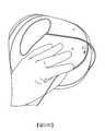
圖22A至圖22L圖解說明根據某些實施例製造一傳輸/接收RF頭部線圈以供在一低場MRI系統中使用之一程序中之動作。圖22A展示根據經編號箭頭自一基板(例如,其中形成有之槽之一塑膠頭盔)之頂部開始之線圈纏繞。舉例而言,導體配置(1)於將基板之頂部連接至一第一圓周槽之一連接槽中。接著在一順時針方向上將導體纏繞(2)在第一圓周槽之一半匝上。圖22B展示在完成(3)第一圓周槽之半匝之後,將導體配置(4)於連接第一圓周槽與一第二圓周槽之一連接槽中,第二圓周槽較第一圓周槽更遠離頂部而間隔開。然後亦在順時針方向上將導體纏繞(5)在第二圓周槽之一對置半匝上。圖22C展示將導體纏繞(6)於第二圓周槽中,直至(7)到達連接第二與第三圓周槽之一連接槽,如圖22D中所展示。然後將導體配置(8)於第二與第三圓周槽之間之連接槽內。圖22E展示纏繞(9)在順時針方向上圍繞一對置半匝於第三圓周槽中繼續,直至(10)到達連接第三與第四圓周槽之一連接槽,如圖22F所展示。然後將導體配置(11)於第三與第四圓周槽之間之連接槽內。圖22G展示纏繞以上文所闡述之半匝型樣繼續,直至到達最底部圓周槽。在某些實施例中,不存在導體在頭盔之一後部側上之交叉,如圖22H中所展示。22A to 22L illustrate actions in a procedure for manufacturing a transmit/receive RF head coil for use in a low field MRI system according to some embodiments. FIG. 22A shows coil winding from the top of a substrate (eg, a plastic helmet with a groove formed therein) according to the numbered arrows. For example, the conductor is arranged (1) in a connecting groove connecting the top of the substrate to a first circumferential groove. Next, the conductor is wound (2) on one and a half turns of the first circumferential slot in a clockwise direction. FIG. 22B shows that after completing (3) a half turn of the first circumferential slot, the conductor is arranged (4) in one of the connecting slots connecting the first circumferential slot and a second circumferential slot, the second circumferential slot is higher than the first circumferential slot Spaced further away from the top. Then, the conductor is also wound (5) in the clockwise direction on one of the opposing half turns of the second circumferential groove. FIG. 22C shows winding the conductor (6) in the second circumferential slot until (7) reaches the connecting slot connecting one of the second and third circumferential slots, as shown in FIG. 22D. Then, the conductor is arranged (8) in the connecting groove between the second and third circumferential grooves. FIG. 22E shows that winding (9) continues in a clockwise direction around a pair of half-turns in the third circumferential groove until (10) reaches a connecting groove connecting one of the third and fourth circumferential grooves, as shown in FIG. 22F. Then, the conductor is arranged (11) in the connecting groove between the third and fourth circumferential grooves. Fig. 22G shows that winding the half-turn pattern explained above continues until it reaches the bottommost circumferential groove. In some embodiments, there is no intersection of conductors on the rear side of one of the helmets, as shown in FIG. 22H.
圖22I展示在完成最底部圓周槽上之纏繞之後,導體之纏繞自底部至頂部在自頂部至底部之纏繞中跳過之圓周槽之部分內繼續。舉例而言,導體纏繞(12)於最底部圓周槽中,導體經配置(13)且交越連接最底部圓周槽與其上方之圓周槽之連接槽內之導體之部分。纏繞(14)於圓周槽中在於頂部至底部纏繞中跳過之部分中繼續。如圖22J中所展示,纏繞(15)繼續直至遭遇下一連接槽,導體經配置(16)且交越彼連接槽內之導體,然後在下一最高圓周槽內繼續(17)。圖22K展示纏繞以相同型樣繼續至基板之頂部,此後切割導體以完成用於具有交錯纏繞之傳輸/接收RF線圈之線圈纏繞,如圖22L中所展示。儘管已將纏繞闡述為係在順時針方向上,但應瞭解,另一選擇係,纏繞可在逆時針方向上進行。此外,儘管圖22A至圖22L中所闡述之程序展示在複數個圓周槽中之每一者中纏繞半匝,但應瞭解,亦可使用其中每一其他圓周槽自頂部至底部跳過且接著自底部至頂部填充之一纏繞型樣。FIG. 22I shows that after the winding on the bottommost circumferential groove is completed, the winding of the conductor continues from the bottom to the top within the portion of the circumferential groove skipped in the winding from the top to the bottom. For example, the conductor is wound (12) in the bottommost circumferential slot, the conductor is arranged (13) and crosses the part of the conductor in the connection slot connecting the bottommost circumferential slot and the circumferential slot above it. The winding (14) continues in the circumferential groove in the portion skipped in the top-to-bottom winding. As shown in FIG. 22J, winding (15) continues until the next connection slot is encountered, the conductor is configured (16) and crosses the conductor in the connection slot, and then continues in the next highest circumferential slot (17). FIG. 22K shows that the winding continues to the top of the substrate in the same pattern, after which the conductor is cut to complete the coil winding for the transmission/reception RF coil with the interleaved winding, as shown in FIG. 22L. Although winding has been described as being tied in a clockwise direction, it should be understood that in another alternative, winding can be done in a counterclockwise direction. In addition, although the procedure illustrated in FIGS. 22A-22L shows winding a half turn in each of the plurality of circumferential grooves, it should be understood that each of the other circumferential grooves can also be used to skip from top to bottom and then Fill one winding pattern from bottom to top.
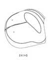
圖23A展示根據某些實施例用於使用一交錯纏繞型樣製造一僅接收RF線圈之一程序。如所展示,線圈纏繞藉由將導體於一連接槽中自基板(例如,其中形成有槽之一塑膠頭盔)之頂部配置(1)至基板之一側(例如,左側)而開始。圖23B展示當導體到達(2)左側上之一環狀槽時,導體纏繞(3)在該環狀槽上。圖23C展示當完成導體圍繞環狀槽之纏繞(4)時,導體經配置(5)且交越連接環狀槽與基板之頂部之連接槽中之導體。如圖23D中所展示,纏繞(6)在形成於頭盔之左半側中之一彎曲槽中繼續。圖23E展示在完成頭盔之左半側中之纏繞之後,導體經配置以交越頭盔之頂部以開始導體在頭盔之右半側上之纏繞,如圖23F中所展示。圖23G及圖23H展示頭盔之右半側中之纏繞圍繞頭盔之右半側中之槽繼續且經配置並交越連接頭盔之右半側上之環狀槽與頭盔之頂部之連接槽中之導體。FIG. 23A shows a process for manufacturing an RF-only coil using a staggered winding pattern according to some embodiments. As shown, the winding of the coil starts by placing (1) the conductor in a connection slot from the top of the substrate (for example, a plastic helmet in which the slot is formed) to one side (for example, the left side) of the substrate. Fig. 23B shows that when the conductor reaches (2) an annular groove on the left side, the conductor is wound (3) on the annular groove. 23C shows that when the winding of the conductor around the annular groove (4) is completed, the conductor is configured (5) and crosses the conductor in the connection groove connecting the annular groove and the top of the substrate. As shown in FIG. 23D, the winding (6) continues in a curved groove formed in the left half of the helmet. FIG. 23E shows that after the winding in the left half of the helmet is completed, the conductor is configured to cross the top of the helmet to start the winding of the conductor on the right half of the helmet, as shown in FIG. 23F. FIGS. 23G and 23H show that the winding in the right half of the helmet continues around the groove in the right half of the helmet and is configured and crossed in the connecting groove connecting the annular groove on the right half of the helmet and the top of the helmet conductor.
因此,已闡述陳述於本發明中之技術之數項態樣及實施例,應瞭解,對於熟悉此項技術者,各種變更、修改及改良將易於發生。此等變更、修改及改良意欲在本文中所闡述之技術之精神及範疇內。舉例而言,熟習此項技術者將易於想像用於執行功能及/或獲得本文中所闡述之結果及/或優點中之一或多者之各種其他構件及/或結構,且此等變化形式及/或修改中之每一者被視為係在本文中所闡述之實施例之範疇內。熟習此項技術者將僅使用常規實驗即可認識或能夠確定本文中所闡述之具體實施例之諸多等效內容。因此,應理解,前述實施例僅以實例方式呈現且在隨附申請專利範圍及其等效物之範疇內,發明性實施例可不同於所具體闡述的來實踐。此外,若本文中所闡述兩個或更多個特徵、系統、物品、材料、套組及/或方法不相互矛盾,則此等特徵、系統、物品、材料、套組及/或方法之任一組合包含於本發明之範疇內。Therefore, several aspects and embodiments of the technology stated in the present invention have been described, and it should be understood that various changes, modifications, and improvements will easily occur to those familiar with the technology. Such changes, modifications, and improvements are intended to be within the spirit and scope of the technology described in this article. For example, those skilled in the art will readily imagine various other components and/or structures for performing functions and/or obtaining one or more of the results and/or advantages set forth herein, and these variations Each and/or modification is considered to be within the scope of the embodiments set forth herein. Those skilled in the art will recognize or be able to determine many equivalents of the specific embodiments set forth herein using only routine experimentation. Therefore, it should be understood that the foregoing embodiments are presented by way of examples only and within the scope of the accompanying patent applications and their equivalents, the inventive embodiments may be practiced differently than specifically set forth. In addition, if two or more features, systems, items, materials, kits, and/or methods described herein do not conflict with each other, then any of these features, systems, items, materials, kits, and/or methods A combination is included in the scope of the present invention.
可以眾多方式中之任一者來實施上文所闡述之實施例。涉及程序或方法之效能之本發明之一或多項態樣及實施例可利用可由一裝置(例如,一電腦、一處理器或其他裝置)執行之程式指令來執行程序或方法或控制其等效能。就此而言,各種發明性概念可體現為一電腦可讀儲存媒體(或多個電腦可讀儲存媒體)(例如,一電腦記憶體、一或多個軟式磁碟、壓縮碟片、光碟、磁帶、快閃記憶體、場可程式化閘陣列或其他半導體裝置中之電路組態、或者其他有形電腦儲存媒體),電腦可讀儲存媒體編碼有當在一或多個電腦或其他處理器上執行時執行實施上文所闡述之各種實施例中之一或多者之方法之一或多個程式。電腦可讀媒體或若干電腦可讀媒體可係可輸送的,使得儲存於其上之程式或若干程式可被載入至一或多個不同電腦或其他處理器上以實施上文所闡述之態樣中之各種態樣。在某些實施例中,電腦可讀媒體可係非暫時性媒體。The embodiments set forth above can be implemented in any of numerous ways. One or more aspects and embodiments of the present invention related to the performance of a program or method can utilize program instructions that can be executed by a device (e.g., a computer, a processor, or other device) to execute the program or method or control its performance . In this regard, various inventive concepts can be embodied as a computer-readable storage medium (or multiple computer-readable storage media) (eg, a computer memory, one or more floppy disks, compact discs, optical discs, magnetic tape , Flash memory, field programmable gate array or other semiconductor device circuit configuration, or other tangible computer storage media), computer-readable storage media encoded when executed on one or more computers or other processors One or more programs that implement one or more of the various embodiments set forth above are executed. The computer-readable medium or computer-readable media may be transportable, so that the program or programs stored thereon can be loaded onto one or more different computers or other processors to implement the state described above All kinds of appearances. In some embodiments, the computer-readable media may be non-transitory media.
術語「程式」或「軟體」在一泛用意義上用於本文中,以指代可用於程式化一電腦或其他處理器來實施如上文所闡述之各種態樣之任何類型之電腦程式碼或電腦可執行指令集。此外,應瞭解,根據一項態樣,在執行時執行本發明之方法之一或多個電腦程式無需駐存於一單個電腦或處理器上,但可以一模組化方式散佈於若干個不同電腦或處理器當中以實施本發明之各種態樣。The term "program" or "software" is used in a general sense in this article to refer to any type of computer code that can be used to program a computer or other processor to implement the various aspects as described above or Computer executable instruction set. In addition, it should be understood that according to one aspect, one or more computer programs that execute the method of the present invention during execution need not reside on a single computer or processor, but may be distributed in a modular manner over several different Various aspects of the invention can be implemented in a computer or processor.
電腦可執行指令可呈由一或多個電腦或其他裝置執行之諸多形式,諸如程式模組。一般而言,程式模組包含執行特定任務或實施特定抽象資料類型之常式、程式、物件、組件、資料結構等。通常,在各種實施例中,可如所期望組合或散佈程式模組之功能性。Computer-executable instructions may take many forms, such as program modules, executed by one or more computers or other devices. In general, program modules include routines, programs, objects, components, data structures, etc. that perform specific tasks or implement specific abstract data types. Generally, in various embodiments, the functionality of the programming module can be combined or distributed as desired.
此外,資料結構可以任何適合形式儲存於電腦可讀媒體中。出於簡化圖解說明之目的,資料結構可經展示以具有透過資料結構中之位置相關之欄位。此等關係同樣可藉由以電腦可讀媒體中之位置為欄位指配儲存區而達成,該等位置傳達欄位之間之關係。然而,任何適合機制可用於在一資料結構之欄位中之資訊之間確立一關係,包含透過使用在資料元素之間確立關係之指標、標籤或其他機制。In addition, the data structure can be stored in a computer-readable medium in any suitable form. For the purpose of simplifying the illustration, the data structure may be shown to have fields that are related by location in the data structure. These relationships can also be achieved by assigning storage areas to locations in the computer-readable medium, which communicate the relationships between the fields. However, any suitable mechanism can be used to establish a relationship between information in a field of a data structure, including through the use of indicators, tags, or other mechanisms that establish relationships between data elements.
可以眾多方式中之任一者來實施本發明之上文所闡述之實施例。舉例而言,實施例可使用硬體、軟體或其一組合來實施。當以軟體實施時,可在任何適合處理器或處理器集合上執行軟體程式碼,無論提供於一單個電腦中或散佈於多個電腦當中。應瞭解,執行上文所闡述之功能之任何組件或組件集合可泛用地視為控制上文所論述之功能之一控制器。一控制器可以眾多方式來實施,諸如藉助專用硬體,或者藉助使用微程式碼或軟體來程式化以執行上文所陳述之功能之一般用途硬體(例如,一或多個處理器),且當控制器對應於一系統之多個組件時可以一方式組合來實施。The above-described embodiments of the present invention can be implemented in any of numerous ways. For example, the embodiments may be implemented using hardware, software, or a combination thereof. When implemented in software, the software code can be executed on any suitable processor or set of processors, whether provided in a single computer or distributed among multiple computers. It should be appreciated that any component or set of components that perform the functions set forth above can be universally considered as a controller that controls the functions discussed above. A controller can be implemented in many ways, such as with dedicated hardware, or with general-purpose hardware (eg, one or more processors) programmed with microcode or software to perform the functions stated above, And when the controller corresponds to multiple components of a system, it can be implemented in a combination.
進一步,應瞭解,作為非限制性實例,一電腦可以若干種形式中之任一者來體現,諸如一機架安裝型電腦、一桌上型電腦、一膝上型電腦或一平板電腦。此外,一電腦可嵌入於一般而言不被視為一電腦但具有適合處理能力之一裝置中,包含一個人數位助理(PDA)、一智慧型電話或任何其他適合可攜式或固定電子裝置。Further, it should be understood that as a non-limiting example, a computer may be embodied in any of several forms, such as a rack-mounted computer, a desktop computer, a laptop computer, or a tablet computer. In addition, a computer can be embedded in a device that is not generally regarded as a computer but has suitable processing capabilities, including a personal assistant (PDA), a smart phone, or any other suitable portable or fixed electronic device.
此外,一電腦可具有一或多個輸入及輸出裝置。除其他事物之外,可使用此等裝置以呈現一使用者介面。可用於提供一使用者介面之輸出裝置之實例包含用於輸出之視覺呈現之印表機或顯示螢幕及用於輸出之聲訊呈現之揚聲器或其他聲音產生裝置。可用於一使用者介面之輸入裝置之實例包含鍵盤及指標裝置,諸如滑鼠、觸控墊及數位化輸入板。作為另一實例,一電腦可透過語音辨識或以其他聲訊格式接收輸入資訊。In addition, a computer may have one or more input and output devices. Among other things, these devices can be used to present a user interface. Examples of output devices that can be used to provide a user interface include printers or display screens for visual presentation of output and speakers or other sound generating devices for audio presentation of output. Examples of input devices that can be used in a user interface include keyboards and pointing devices, such as mice, touchpads, and digital input pads. As another example, a computer can receive input information through voice recognition or in other audio formats.
此等電腦可藉由一或多個網路以任何適合形式互連,包含一區域網路或一廣域網路,諸如一企業網路,及智慧型網路(IN)或網際網路。此等網路可係基於任何適合技術且可根據任何適合協定操作並且可包含無線網路、有線網路或光纖網路。These computers can be interconnected in any suitable form by one or more networks, including a local area network or a wide area network, such as an enterprise network, and an intelligent network (IN) or the Internet. These networks can be based on any suitable technology and can operate according to any suitable protocol and can include wireless networks, wired networks, or fiber optic networks.
此外,如所闡述,某些態樣可體現為一或多種方法。作為方法之部分執行之動作可以任一適合方式來排序。因此,實施例可經構建,其中以不同於所圖解說明之一次序執行動作,其可包含同時執行某些動作,即使在說明性實施例中展示為依序動作。In addition, as stated, certain aspects may be embodied in one or more methods. The actions performed as part of the method can be ordered in any suitable way. Accordingly, embodiments may be constructed in which actions are performed in an order different from that illustrated, which may include performing certain actions simultaneously, even if shown as sequential actions in the illustrative embodiment.
本文中所定義及所使用之所有定義應理解為控制在辭典定義、以引用方式併入之文件中之定義及/或所定義術語之常規意義以內。All definitions defined and used herein should be understood to control within dictionary definitions, definitions in documents incorporated by reference, and/or conventional meanings of the defined terms.
除非明確指示為相反,否則如本文中在說明書及在申請專利範圍中所使用之不定冠詞「一(a)」及「一(an)」應理解為意指「至少一個」。Unless expressly indicated to the contrary, the indefinite articles "a" and "an" as used herein in the specification and in the scope of patent application should be understood to mean "at least one".
如本文中在說明書及在申請專利範圍中所使用之片語「及/或」應理解為意指如此結合之元件中之「任一者或兩者」,亦即,在某些情形中以結合方式存在且在其他情形中以分離方式存在之元件。以「及/或」列舉之多個元件應視為呈相同方式,亦即,如此結合之元件中之「一或多者」。可視情況存在除由「及/或」從句特定識別之元件以外的其他元件,無論與特定識別之彼等元件相關還是不相關。因此,作為一非限定性實例,當結合諸如「包括」之開放式語言使用時,在一項實施例中,對「A及/或B」之一提及可係指僅A (視情況包含除B以外之元件);在另一實施例中,係指僅B (視情況包含除A以外之元件);在仍另一實施例中,係指A及B兩者(視情況包含其他元件);等等。The phrase "and/or" as used herein in the specification and in the scope of patent application should be understood to mean "any or both" of the elements so combined, that is, in some cases Elements that exist in a combined manner and exist in a separate manner in other situations. Multiple elements listed with "and/or" shall be considered in the same manner, that is, "one or more" of the elements so combined. There may be elements other than those specifically identified by the "and/or" clause, regardless of whether they are related or not related to those elements specifically identified. Therefore, as a non-limiting example, when used in conjunction with an open language such as "include", in one embodiment, a reference to one of "A and/or B" may refer to only A (as appropriate Elements other than B); in another embodiment, it means only B (optionally including elements other than A); in still another embodiment, it refers to both A and B (optionally including other elements) );and many more.
如本文中在說明書中及在申請專利範圍中所使用,參考一或多個元素之一清單之片語「至少一個」應理解為意指選自元件清單中之任一或多個元件中之至少一個元件,但未必包含元件清單內特定列出之每一(each)及每一(every)元件中之至少一者,且不排除元件清單中元件之任何組合。此定義亦允許可視情況存在除片語「至少一個」所指之元件清單內特定識別之元件之外之元件,無論與特定識別之彼等元件相關還是不相關。因此,作為一非限定性實例,在一項實施例中,「A及B中之至少一者」(或等效地,「A或B中之至少一者」,或等效地,「A及/或B中之至少一者」)可係指至少一個(視情況包含一個以上) A,而不存在B (且視情況包含除B以外之元件);在另一實施例中,係指至少一個(視情況包含一個以上) B,而不存在A (且視情況包含除A以外之元件);在仍另一實施例中,係指至少一個(視情況包含一個以上) A及至少一個(視情況包含一個以上) B (且視情況包含其他元件);等等。As used herein in the specification and in the scope of patent applications, the phrase "at least one" referring to a list of one or more elements should be understood to mean any one or more elements selected from the list of elements At least one element, but does not necessarily include at least one of each and every element specifically listed in the element list, and does not exclude any combination of elements in the element list. This definition also allows for the existence of components other than those specifically identified in the list of components referred to by the phrase "at least one", regardless of whether they are related or not related to those components specifically identified. Therefore, as a non-limiting example, in one embodiment, "at least one of A and B" (or equivalently, "at least one of A or B", or equivalently, "A And/or at least one of B") may refer to at least one (optionally including more than one) A without B (and optionally including elements other than B); in another embodiment, it refers to At least one (optionally including more than one) B, without A (and optionally including elements other than A); in yet another embodiment, means at least one (optionally including more than one) A and at least one (Contains more than one as appropriate) B (and optionally contains other components); etc.
此外,本文中所使用之措辭及術語係出於闡述目的且不應視為限制性的。本文中使用「包含(including)」、「包括(comprising)」、「具有(having)」、「含有(containing)」、「涉及(involving)」及其變化形式意指囊括其後所列之項目及其等效物以及額外項目。In addition, the wording and terminology used herein are for illustrative purposes and should not be considered limiting. The use of ``including'', ``comprising'', ``having'', ``containing'', ``involving'' and their variations in this article means including the items listed below And their equivalents and additional items.
在申請專利範圍以及在上文說明書中,所有過渡性片語(諸如「包括」、「包含」、「攜載(carrying)」、「具有」、「含有」、「涉及」、「固持(holding)」、「由……構成(composed of)」及諸如此類)應理解為係開放式的,亦即,意指包含但不限於。僅過渡性片語「由……組成(consisting of)」及「基本上由……組成(consisting essentially of)」應分別係封閉式或半封閉式過渡性片語。In the scope of patent application and in the above description, all transitional phrases (such as "include", "include", "carrying", "have", "contain", "involve", "holding" )", "composed of" and the like) should be understood to be open-ended, that is, to include but not limited to. Only transitional phrases "consisting of" and "consisting essentially of" should be closed or semi-closed transitional phrases, respectively.
1:配置2:纏繞/到達3:完成/纏繞4:配置/纏繞5:纏繞/配置6:纏繞7:直至8:配置9:纏繞10:直至11:配置12:纏繞13:配置14:纏繞15:纏繞16:配置17:繼續100:磁共振成象系統/系統/低場磁共振成像系統104:運算裝置106:控制器108:脈衝序列儲存裝置110:電力管理系統112:電力供應器114:電力組件116:傳輸/接收開關118:熱管理組件120:磁性組件122:B0磁體/磁體124:勻場線圈126:射頻傳輸及接收線圈/線圈/射頻接收線圈128:梯度線圈200:射頻信號鏈電路210:射頻傳輸/接收線圈/射頻線圈/組件212:傳輸/接收電路214:調諧/匹配電路/組件216:放大器/組件300:被動解耦電路/電路/解耦電路312:傳輸/接收開關400:解耦電路/電路412:射頻傳輸/接收開關電路/電路500:基於回饋之解耦電路/解耦電路/電路600:替代基於回饋之解耦電路/電路700:電路1000:電路1100:驅動電路/電路2100:程序2110:動作2112:動作2114:動作2116:動作C_ds:經集總電容器C_gd:經集總電容器C_gs:經集總電容器C1:電容器/單個電容器/電抗組件/組件C2:電容器/電抗組件C3:電容器/組件C7:電容器D:汲極節點/汲極D1:二極體D3:二極體F1:鏡像場效應電晶體F2:鏡像場效應電晶體G:閘極h:距離L1:電感器/組件L2:電感器/組件L5:電感器L6:電感器/線圈/脈衝接收器線圈R1:組件/加偏壓電阻器R2:組件R11:電阻器S:源極節點/源極U1:氮化鎵場效應電晶體/場效應電晶體U2:氮化鎵場效應電晶體/場效應電晶體V0:電壓源V2:控制信號/外部提供之控制信號V+:點/導體/各別點/輸出V-:點/導體/各別點/輸出Zc:阻抗/寄生耦合/弱寄生耦合Z+:阻抗/弱寄生耦合Z-:阻抗/弱寄生耦合1: configuration2: winding/arrival3: finish/wind4: configuration/winding5: winding/configuration6: winding7: Until8: configuration9: winding10: Until11: Configuration12: winding13: Configuration14: winding15: winding16: Configuration17: continue100: Magnetic resonance imaging system/system/low-field magnetic resonance imaging system104: computing device106: controller108: Pulse sequence storage device110: Power management system112: Power supply114: Power components116: Transmit/receive switch118: Thermal management components120: Magnetic components122: B0 magnet/magnet124: shim coil126: RF transmission and receiving coil/coil/RF receiving coil128: gradient coil200: RF signal chain circuit210: RF transmission/reception coil/RF coil/component212: Transmission/reception circuit214: Tuning/matching circuit/component216: Amplifier/Component300: Passive decoupling circuit/circuit/decoupling circuit312: Transmit/receive switch400: decoupling circuit/circuit412: RF transmission/reception switching circuit/circuit500: feedback-based decoupling circuit/decoupling circuit/circuit600: Replace the decoupling circuit/circuit based on feedback700: Circuit1000: circuit1100: drive circuit/circuit2100: Procedure2110: Action2112: Action2114: Action2116: ActionC_ds: warped lumped capacitorC_gd: warped lumped capacitorC_gs: warped lumped capacitorC1: capacitor/single capacitor/reactive component/componentC2: Capacitor/reactive componentC3: capacitor/componentC7: CapacitorD: Drain node/DrainD1: DiodeD3: DiodeF1: Mirror field effect transistorF2: Mirror field effect transistorG: gateh: distanceL1: inductor/componentL2: inductor/componentL5: inductorL6: inductor/coil/pulse receiver coilR1: component/bias resistorR2: ComponentsR11: resistorS: source node/sourceU1: GaN field effect transistor/field effect transistorU2: GaN field effect transistor/field effect transistorV0: voltage sourceV2: control signal / externally provided control signalV+: point/conductor/each point/outputV-: point/conductor/each point/outputZc: impedance/parasitic coupling/weak parasitic couplingZ+: impedance/weak parasitic couplingZ-: impedance/weak parasitic coupling
將參考以下各圖闡述所揭示技術之各種態樣及實施例。應瞭解,各圖未必按比例繪製。Various aspects and embodiments of the disclosed technology will be explained with reference to the following figures. It should be understood that the figures are not necessarily drawn to scale.
圖1圖解說明一磁共振成像系統之例示性組件;FIG. 1 illustrates exemplary components of a magnetic resonance imaging system;
圖2圖解說明用於一磁共振成像系統之一RF信號鏈之組件;Figure 2 illustrates the components of an RF signal chain for a magnetic resonance imaging system;
圖3圖解說明供在一磁共振成像系統之一RF信號鏈內使用之解耦電路;Figure 3 illustrates a decoupling circuit for use in an RF signal chain of a magnetic resonance imaging system;
圖4A及圖4B展示與圖3之解耦電路相關聯之模擬資料;4A and 4B show simulation data associated with the decoupling circuit of FIG. 3;
圖5圖解說明根據某些實施例使用放大器回饋之解耦電路;FIG. 5 illustrates a decoupling circuit using amplifier feedback according to certain embodiments;
圖6圖解說明根據某些實施例之圖5之解耦電路,其中一單個電容器用於提供線圈調諧;6 illustrates the decoupling circuit of FIG. 5 according to some embodiments, in which a single capacitor is used to provide coil tuning;
圖7A及圖7B展示與圖6之解耦電路相關聯之模擬資料;7A and 7B show the simulation data associated with the decoupling circuit of FIG. 6;
圖8圖解說明根據某些實施例之圖5之解耦電路,其中一調諧/匹配網路用於提供線圈調諧;FIG. 8 illustrates the decoupling circuit of FIG. 5 according to some embodiments, wherein a tuning/matching network is used to provide coil tuning;
圖9圖解說明用於供在一磁共振成像系統之一RF信號鏈中使用之一基於二極體之開關之電路;9 illustrates a circuit for a diode-based switch for use in an RF signal chain of a magnetic resonance imaging system;
圖10圖解說明根據某些實施例用於供在一磁共振成像系統之一RF信號鏈中使用之一基於FET之開關之電路;10 illustrates a circuit for an FET-based switch for use in an RF signal chain of a magnetic resonance imaging system according to some embodiments;
圖11A至圖11C圖解說明圖10之基於FET之開關中一FET之操作條件;11A to 11C illustrate the operating conditions of one FET in the FET-based switch of FIG. 10;
圖12圖解說明根據某些實施例用於供在一磁共振成像系統之一RF信號鏈中使用之一基於GaN FET之開關之電路;12 illustrates a circuit for a GaN FET-based switch for use in an RF signal chain of a magnetic resonance imaging system according to certain embodiments;
圖13圖解說明根據某些實施例用於供在一磁共振成像系統之一RF信號鏈中使用之一基於GaN FET之開關之電路;13 illustrates a circuit for a GaN FET-based switch for use in an RF signal chain of a magnetic resonance imaging system according to certain embodiments;
圖14A圖解說明用於一RF線圈之一單通纏繞設計;14A illustrates a one-pass winding design for an RF coil;
圖14B圖解說明圖14A之單通纏繞設計之一俯視圖;14B illustrates a top view of one-pass winding design of FIG. 14A;
圖15A圖解說明根據某些實施例連接至供在一低場MRI系統中使用之一放大器之一RF線圈之一示意圖;15A illustrates a schematic diagram of an RF coil connected to an amplifier for use in a low-field MRI system according to some embodiments;
圖15B圖解說明根據某些實施例用於表示與一物件至一RF線圈之一寄生耦合相關聯之阻抗之一阻抗模型;15B illustrates an impedance model used to represent the impedance associated with a parasitic coupling of an object to an RF coil according to some embodiments;
圖16A圖解說明根據某些實施例用於一RF線圈之一交錯纏繞設計;16A illustrates an interleaved winding design for an RF coil according to some embodiments;
圖16B圖解說明圖16A之交錯纏繞設計之一俯視圖;16B illustrates a top view of the interleaved winding design of FIG. 16A;
圖17A圖解說明根據某些實施例用於一RF線圈之一替代交錯纏繞設計;17A illustrates an alternative interlaced winding design for one of the RF coils according to some embodiments;
圖17B圖解說明圖17A之交錯纏繞設計之一俯視圖;17B illustrates a top view of the interlaced winding design of FIG. 17A;
圖18A圖解說明根據某些實施例用於一RF線圈之一雙迴路纏繞設計;18A illustrates a dual-loop winding design for an RF coil according to some embodiments;
圖18B圖解說明圖18A之雙迴路纏繞設計之一俯視圖;18B illustrates a top view of one of the dual loop winding designs of FIG. 18A;
圖19圖解說明根據某些實施例用於一RF線圈之一逆螺旋式纏繞設計之一俯視圖;FIG. 19 illustrates a top view of a reverse spiral winding design for an RF coil according to certain embodiments;
圖20圖解說明根據某些實施例用於一RF表面線圈之一平衡式纏繞設計;20 illustrates a balanced winding design for an RF surface coil according to certain embodiments;
圖21圖解說明根據某些實施例用於形成具有一平衡式纏繞型樣之一RF線圈之一程序;21 illustrates a procedure for forming an RF coil having a balanced winding pattern according to some embodiments;
圖22A至圖22L圖解說明根據某些實施例用於形成具有一交錯纏繞型樣之一RF線圈之一程序中之動作;22A to 22L illustrate actions in a procedure for forming an RF coil having a staggered winding pattern according to some embodiments;
圖23A至圖23H圖解說明根據某些實施例用於形成具有一替代交錯纏繞型樣之一RF線圈之一程序中之動作;及23A to 23H illustrate actions in a procedure for forming an RF coil having an alternate interlaced pattern according to certain embodiments; and
圖24圖解說明根據某些實施例使用互感回饋之解耦電路。FIG. 24 illustrates a decoupling circuit that uses mutual inductive feedback according to some embodiments.
400:解耦電路/電路400: decoupling circuit/circuit
Claims (37)
Translated fromChineseApplications Claiming Priority (4)
| Application Number | Priority Date | Filing Date | Title |
|---|---|---|---|
| US201862674458P | 2018-05-21 | 2018-05-21 | |
| US62/674,458 | 2018-05-21 | ||
| US201862692454P | 2018-06-29 | 2018-06-29 | |
| US62/692,454 | 2018-06-29 |
Publications (1)
| Publication Number | Publication Date |
|---|---|
| TW202011687Atrue TW202011687A (en) | 2020-03-16 |
Family
ID=66821421
Family Applications (1)
| Application Number | Title | Priority Date | Filing Date |
|---|---|---|---|
| TW108117535ATW202011687A (en) | 2018-05-21 | 2019-05-21 | Radio-frequency coil signal chain for a low-field MRI system |
Country Status (12)
| Country | Link |
|---|---|
| US (7) | US10969446B2 (en) |
| EP (1) | EP3797308A1 (en) |
| JP (1) | JP2021526043A (en) |
| KR (1) | KR20210013567A (en) |
| CN (1) | CN112384818A (en) |
| AU (1) | AU2019272580A1 (en) |
| BR (1) | BR112020021579A2 (en) |
| CA (1) | CA3099068A1 (en) |
| IL (1) | IL278776A (en) |
| MX (1) | MX2020012542A (en) |
| TW (1) | TW202011687A (en) |
| WO (1) | WO2019226624A1 (en) |
Families Citing this family (39)
| Publication number | Priority date | Publication date | Assignee | Title |
|---|---|---|---|---|
| BR112017004353A2 (en) | 2014-09-05 | 2017-12-05 | Hyperfine Res Inc | ferromagnetic magnification for magnetic resonance imaging |
| CN105591537B (en)* | 2014-10-28 | 2019-02-22 | 通用电气公司 | Gradient amplifier, switching amplifier and method of operation thereof |
| WO2016077417A1 (en) | 2014-11-11 | 2016-05-19 | Hyperfine Research, Inc. | Low field magnetic resonance methods and apparatus |
| AU2015346431B2 (en) | 2014-11-11 | 2020-06-18 | Hyperfine Operations, Inc. | Pulse sequences for low field magnetic resonance |
| BR112017021999A2 (en) | 2015-04-13 | 2018-07-10 | Hyperfine Res Inc | magnetic coil feeding apparatus and methods |
| US10709387B2 (en) | 2015-05-12 | 2020-07-14 | Hyperfine Research, Inc. | Radio frequency coil methods and apparatus |
| CN109073681B (en) | 2016-03-22 | 2020-10-23 | 海珀菲纳研究股份有限公司 | Method and apparatus for magnetic field shimming |
| TWI667487B (en) | 2016-09-29 | 2019-08-01 | 美商超精細研究股份有限公司 | Radio frequency coil tuning methods and apparatus |
| US10539637B2 (en) | 2016-11-22 | 2020-01-21 | Hyperfine Research, Inc. | Portable magnetic resonance imaging methods and apparatus |
| US10627464B2 (en) | 2016-11-22 | 2020-04-21 | Hyperfine Research, Inc. | Low-field magnetic resonance imaging methods and apparatus |
| US10718842B2 (en) | 2016-11-22 | 2020-07-21 | Hyperfine Research, Inc. | Systems and methods for automated detection in magnetic resonance images |
| TWI744629B (en) | 2018-04-20 | 2021-11-01 | 美商海珀菲纳股份有限公司 | Deployable guard devices and apparatus and system comprising the same |
| MX2020012537A (en) | 2018-05-21 | 2021-02-16 | Hyperfine Res Inc | B<sub>0</sub> MAGNET METHODS AND APPARATUS FOR A MAGNETIC RESONANCE IMAGING SYSTEM. |
| TW202011687A (en) | 2018-05-21 | 2020-03-16 | 美商超精細研究股份有限公司 | Radio-frequency coil signal chain for a low-field MRI system |
| TW202015621A (en) | 2018-07-19 | 2020-05-01 | 美商超精細研究股份有限公司 | Methods and apparatus for patient positioning in magnetic resonance imaging |
| CN120370238A (en) | 2018-07-30 | 2025-07-25 | 海珀菲纳股份有限公司 | System, method, storage medium and magnetic resonance imaging system for a deep learning technique for magnetic resonance image reconstruction |
| TW202012951A (en) | 2018-07-31 | 2020-04-01 | 美商超精細研究股份有限公司 | Low-field diffusion weighted imaging |
| AU2019321607A1 (en) | 2018-08-15 | 2021-02-11 | Hyperfine Operations, Inc. | Deep learning techniques for suppressing artefacts in magnetic resonance images |
| EP3899565A2 (en) | 2018-12-19 | 2021-10-27 | Hyperfine, Inc. | System and methods for grounding patients during magnetic resonance imaging |
| JP2022515825A (en) | 2018-12-28 | 2022-02-22 | ハイパーファイン,インコーポレイテッド | Hysteresis correction in magnetic resonance imaging |
| KR20210137142A (en) | 2019-03-12 | 2021-11-17 | 하이퍼파인, 인크. | Systems and methods for magnetic resonance imaging of infants |
| US11185249B2 (en) | 2019-03-14 | 2021-11-30 | Hyperfine, Inc. | Self ensembling techniques for generating magnetic resonance images from spatial frequency data |
| EP3959529A1 (en) | 2019-04-26 | 2022-03-02 | Hyperfine, Inc. | Techniques for dynamic control of a magnetic resonance imaging system |
| WO2020227054A1 (en) | 2019-05-07 | 2020-11-12 | Hyperfine Research, Inc. | Systems, devices, and methods for magnetic resonance imaging of infants |
| EP4014057A1 (en) | 2019-08-15 | 2022-06-22 | Hyperfine Operations, Inc. | Eddy current mitigation systems and methods |
| US11986282B2 (en) | 2019-10-08 | 2024-05-21 | Hyperfine Operations, Inc. | System and methods for detecting electromagnetic interference in patients during magnetic resonance imaging |
| DE102019127466B4 (en)* | 2019-10-11 | 2022-08-25 | Albert-Ludwigs-Universität Freiburg | Magnetic coil for an MR device |
| US20210124001A1 (en) | 2019-10-25 | 2021-04-29 | Hyperfine Research, Inc. | Systems and methods for detecting patient motion during magnetic resonance imaging |
| US20210123998A1 (en) | 2019-10-25 | 2021-04-29 | Hyperfine Research, Inc. | Artefact reduction in magnetic resonance imaging |
| US11510588B2 (en) | 2019-11-27 | 2022-11-29 | Hyperfine Operations, Inc. | Techniques for noise suppression in an environment of a magnetic resonance imaging system |
| US11415651B2 (en) | 2019-12-10 | 2022-08-16 | Hyperfine Operations, Inc. | Low noise gradient amplification components for MR systems |
| US11422213B2 (en) | 2019-12-10 | 2022-08-23 | Hyperfine Operations, Inc. | Ferromagnetic frame for magnetic resonance imaging |
| USD932014S1 (en) | 2019-12-10 | 2021-09-28 | Hyperfine, Inc. | Frame for magnets in magnetic resonance imaging |
| EP4073530A1 (en) | 2019-12-10 | 2022-10-19 | Hyperfine Operations, Inc. | Permanent magnet assembly for magnetic resonance imaging with non-ferromagnetic frame |
| USD912822S1 (en) | 2019-12-10 | 2021-03-09 | Hyperfine Research, Inc. | Frame for magnets in magnetic resonance imaging |
| WO2021195101A1 (en) | 2020-03-24 | 2021-09-30 | Hyperfine, Inc. | Gradient waveform design for low-field magnetic resonance imaging systems |
| WO2022055808A1 (en) | 2020-09-08 | 2022-03-17 | Hyperfine, Inc. | Systems and methods for providing operating power to an magnetic resonance imaging (mri) system |
| EP4264304A1 (en) | 2020-12-15 | 2023-10-25 | Hyperfine Operations, Inc. | Opto-isolator circuitry for magnetic resonance imaging applications |
| DE102022206766B3 (en)* | 2022-07-01 | 2023-11-30 | Bruker Switzerland Ag | NMR probe head with a transmitting/receiving coil comprising a forward winding section and a rewinding section |
Family Cites Families (62)
| Publication number | Priority date | Publication date | Assignee | Title |
|---|---|---|---|---|
| FI80346C (en)* | 1983-07-07 | 1990-05-10 | Instrumentarium Oy | RF-SPOLARRANGEMANG VID NMR-UNDERSOEKNINGSAPPARATUR. |
| US4961054A (en)* | 1989-07-06 | 1990-10-02 | General Electric Company | Gradient current speed-up circuit for high-speed NMR imaging system |
| FR2653618B1 (en)* | 1989-10-24 | 1992-02-07 | Sorep Sa | BALANCED CIRCUIT OF PHASE SUPPLYING FROM A RADIO FREQUENCY SIGNAL TO A REFERENCE SIGNAL. |
| US5051700A (en) | 1990-03-19 | 1991-09-24 | Kabushiki Kaisha Toshiba | Feedback circuit for noiseless damping of the Q of an MRI receiver coil antenna |
| JPH06254071A (en)* | 1993-03-10 | 1994-09-13 | Toshiba Corp | Magnetic resonance video device and probe for magnetic resonance video device |
| WO1997046895A1 (en)* | 1996-06-03 | 1997-12-11 | Samuel Roznitsky | Antenna system for nmr and mri apparatus |
| US6144205A (en) | 1998-11-19 | 2000-11-07 | General Electric Company | Optical control of radio frequency antennae in a magnetic resonance imaging system |
| US6459265B1 (en)* | 1998-11-25 | 2002-10-01 | General Electric Company | Method and apparatus for reducing input impedance of a preamplifier |
| US6493572B1 (en)* | 1999-09-30 | 2002-12-10 | Toshiba America Mri, Inc. | Inherently de-coupled sandwiched solenoidal array coil |
| US7196519B2 (en) | 2000-07-28 | 2007-03-27 | Fonar Corporation | Stand-up vertical field MRI apparatus |
| US6498489B1 (en) | 2001-05-04 | 2002-12-24 | Kamal Vij | Magnetic resonance imaging coil arrays with separable imaging coil elements |
| ITSV20010039A1 (en) | 2001-10-31 | 2003-05-01 | Esaote Spa | CIRCUIT FOR DE-DISCONNECTION OF TRANSMISSION COILS IN MACHINES FOR THE DETECTION OF RESONANCE IMAGES |
| EP1585990A1 (en) | 2003-01-07 | 2005-10-19 | Philips Intellectual Property & Standards GmbH | High-frequency system for an mr apparatus with multiple transmit channels |
| EP1651974B8 (en) | 2003-07-09 | 2011-11-02 | Inc. Vista Clara | Multicoil nmr data acquisition and processing methods |
| JP2005073335A (en)* | 2003-08-21 | 2005-03-17 | Sony Corp | Switching power supply circuit |
| WO2005083458A1 (en)* | 2004-02-26 | 2005-09-09 | National Research Council Of Canada | Method of effecting nuclear magnetic resonance experiments using cartesian feedback |
| US7242274B2 (en)* | 2004-03-03 | 2007-07-10 | Atheros Communications, Inc. | Inductor layout using step symmetry for inductors |
| EP3462203B1 (en)* | 2004-09-16 | 2022-11-16 | Koninklijke Philips N.V. | Magnetic resonance receive coil with dynamic range control |
| WO2006137946A2 (en) | 2004-11-23 | 2006-12-28 | M2M Imaging Corp. | Coil decoupling in magnetic resonance imaging |
| US7683619B2 (en) | 2005-09-09 | 2010-03-23 | The State of Oregen Acting by and through the State Board of Higher Education on Behalf of the University of Oregon | High impedance differential input preamplifier and antenna for MRI |
| US20100141257A1 (en)* | 2007-05-04 | 2010-06-10 | Koninklijke Philips Electronics N.V. | Rf transmitter with digital feedback for mri |
| EP2229097A4 (en) | 2007-11-09 | 2011-01-26 | Vista Clara Inc | Multicoil low-field nuclear magnetic resonance detection and imaging apparatus and method |
| CN101878432A (en)* | 2007-11-30 | 2010-11-03 | 皇家飞利浦电子股份有限公司 | The MR coil that has active electronic component with indirect power connection |
| US8198895B2 (en)* | 2009-09-23 | 2012-06-12 | General Electric Company | System and method for magnetic resonance coil actuation |
| US8294465B2 (en)* | 2010-03-31 | 2012-10-23 | Natalia Gudino | Switched mode pre-amplification and am feedback for on-coil switched mode amplifiers in parallel transmission MRI |
| US20150005618A1 (en) | 2011-01-04 | 2015-01-01 | Children's Hospital Medical Center | MRI Transfer Station |
| US8749237B2 (en) | 2011-01-11 | 2014-06-10 | General Electric Company | Optically controlled MEMS switch and method of using the same |
| EP2715386A1 (en)* | 2011-05-23 | 2014-04-09 | Koninklijke Philips N.V. | Fet switch as detune circuit for mri rf coils |
| US9989604B2 (en)* | 2012-12-24 | 2018-06-05 | Case Western Reserve University | Multiturn MRI coils in combination with current mode class D amplifiers |
| US9714992B2 (en) | 2014-01-23 | 2017-07-25 | Shahin Pourrahimi | Versatile superconducting magnet for extremities magnetic resonance imaging |
| US9536423B2 (en)* | 2013-03-31 | 2017-01-03 | Case Western Reserve University | Fiber optic telemetry for switched-mode current-source amplifier in magnetic resonance imaging (MRI) |
| EP2903146B1 (en)* | 2014-02-03 | 2019-03-20 | STMicroelectronics Srl | Monophase or polyphase resonant converter with feedback control |
| CA2942390A1 (en)* | 2014-03-14 | 2015-09-17 | The General Hospital Corporation | System and method for low-field, multi-channel imaging |
| RU2685057C2 (en) | 2014-03-31 | 2019-04-16 | Конинклейке Филипс Н.В. | Magnetic resonance imaging with rf noise detection coils |
| BR112017004353A2 (en) | 2014-09-05 | 2017-12-05 | Hyperfine Res Inc | ferromagnetic magnification for magnetic resonance imaging |
| WO2016077417A1 (en) | 2014-11-11 | 2016-05-19 | Hyperfine Research, Inc. | Low field magnetic resonance methods and apparatus |
| AU2015346431B2 (en) | 2014-11-11 | 2020-06-18 | Hyperfine Operations, Inc. | Pulse sequences for low field magnetic resonance |
| BR112017021999A2 (en) | 2015-04-13 | 2018-07-10 | Hyperfine Res Inc | magnetic coil feeding apparatus and methods |
| DE102015207990B4 (en)* | 2015-04-30 | 2016-12-08 | Siemens Healthcare Gmbh | Detuning of an MRI receiving antenna |
| US10709387B2 (en) | 2015-05-12 | 2020-07-14 | Hyperfine Research, Inc. | Radio frequency coil methods and apparatus |
| CN109073681B (en) | 2016-03-22 | 2020-10-23 | 海珀菲纳研究股份有限公司 | Method and apparatus for magnetic field shimming |
| US10852373B2 (en)* | 2016-09-21 | 2020-12-01 | Quality Electrodynamics, Llc | Modulating magnetic resonance imaging transmit field in magnetic resonance fingerprinting using single layer transmit/receive radio frequency coil |
| TWI667487B (en) | 2016-09-29 | 2019-08-01 | 美商超精細研究股份有限公司 | Radio frequency coil tuning methods and apparatus |
| US10718842B2 (en) | 2016-11-22 | 2020-07-21 | Hyperfine Research, Inc. | Systems and methods for automated detection in magnetic resonance images |
| US10539637B2 (en) | 2016-11-22 | 2020-01-21 | Hyperfine Research, Inc. | Portable magnetic resonance imaging methods and apparatus |
| US10585153B2 (en) | 2016-11-22 | 2020-03-10 | Hyperfine Research, Inc. | Rotatable magnet methods and apparatus for a magnetic resonance imaging system |
| US10627464B2 (en) | 2016-11-22 | 2020-04-21 | Hyperfine Research, Inc. | Low-field magnetic resonance imaging methods and apparatus |
| TWI744629B (en) | 2018-04-20 | 2021-11-01 | 美商海珀菲纳股份有限公司 | Deployable guard devices and apparatus and system comprising the same |
| TW202011687A (en) | 2018-05-21 | 2020-03-16 | 美商超精細研究股份有限公司 | Radio-frequency coil signal chain for a low-field MRI system |
| MX2020012537A (en) | 2018-05-21 | 2021-02-16 | Hyperfine Res Inc | B<sub>0</sub> MAGNET METHODS AND APPARATUS FOR A MAGNETIC RESONANCE IMAGING SYSTEM. |
| TW202015621A (en) | 2018-07-19 | 2020-05-01 | 美商超精細研究股份有限公司 | Methods and apparatus for patient positioning in magnetic resonance imaging |
| CN120370238A (en) | 2018-07-30 | 2025-07-25 | 海珀菲纳股份有限公司 | System, method, storage medium and magnetic resonance imaging system for a deep learning technique for magnetic resonance image reconstruction |
| TW202012951A (en) | 2018-07-31 | 2020-04-01 | 美商超精細研究股份有限公司 | Low-field diffusion weighted imaging |
| JP2021532885A (en) | 2018-07-31 | 2021-12-02 | ハイパーファイン,インコーポレイテッド | Medical Imaging Equipment Messaging Service |
| AU2019321607A1 (en) | 2018-08-15 | 2021-02-11 | Hyperfine Operations, Inc. | Deep learning techniques for suppressing artefacts in magnetic resonance images |
| EP3899565A2 (en) | 2018-12-19 | 2021-10-27 | Hyperfine, Inc. | System and methods for grounding patients during magnetic resonance imaging |
| JP2022515825A (en) | 2018-12-28 | 2022-02-22 | ハイパーファイン,インコーポレイテッド | Hysteresis correction in magnetic resonance imaging |
| KR20210137142A (en) | 2019-03-12 | 2021-11-17 | 하이퍼파인, 인크. | Systems and methods for magnetic resonance imaging of infants |
| US11185249B2 (en) | 2019-03-14 | 2021-11-30 | Hyperfine, Inc. | Self ensembling techniques for generating magnetic resonance images from spatial frequency data |
| WO2020227054A1 (en) | 2019-05-07 | 2020-11-12 | Hyperfine Research, Inc. | Systems, devices, and methods for magnetic resonance imaging of infants |
| EP4334732A1 (en) | 2021-05-05 | 2024-03-13 | Neuro42 Inc. | Neural interventional magnetic resonance imaging apparatus |
| US12270867B2 (en) | 2022-11-19 | 2025-04-08 | Neuro42 Inc. | System and method for removing electromagnetic interference from low-field magnetic resonance images |
- 2019
- 2019-05-21TWTW108117535Apatent/TW202011687A/enunknown
- 2019-05-21KRKR1020207034056Apatent/KR20210013567A/ennot_activeWithdrawn
- 2019-05-21AUAU2019272580Apatent/AU2019272580A1/ennot_activeAbandoned
- 2019-05-21WOPCT/US2019/033269patent/WO2019226624A1/ennot_activeCeased
- 2019-05-21BRBR112020021579-1Apatent/BR112020021579A2/ennot_activeApplication Discontinuation
- 2019-05-21CNCN201980034207.1Apatent/CN112384818A/enactivePending
- 2019-05-21CACA3099068Apatent/CA3099068A1/ennot_activeAbandoned
- 2019-05-21MXMX2020012542Apatent/MX2020012542A/enunknown
- 2019-05-21USUS16/418,414patent/US10969446B2/enactiveActive
- 2019-05-21EPEP19729996.9Apatent/EP3797308A1/enactivePending
- 2019-05-21USUS16/418,379patent/US10890634B2/enactiveActive
- 2019-05-21JPJP2020564709Apatent/JP2021526043A/enactivePending
- 2019-05-21USUS16/418,397patent/US10871530B2/enactiveActive
- 2020
- 2020-11-10USUS17/094,301patent/US11378630B2/enactiveActive
- 2020-11-17ILIL278776Apatent/IL278776A/enunknown
- 2020-12-02USUS17/109,320patent/US20210116520A1/ennot_activeAbandoned
- 2021
- 2021-02-23USUS17/182,777patent/US11662402B2/enactiveActive
- 2023
- 2023-04-24USUS18/138,283patent/US12436212B2/enactiveActive
Also Published As
| Publication number | Publication date |
|---|---|
| MX2020012542A (en) | 2021-02-16 |
| KR20210013567A (en) | 2021-02-04 |
| US20210080524A1 (en) | 2021-03-18 |
| US11662402B2 (en) | 2023-05-30 |
| US10871530B2 (en) | 2020-12-22 |
| BR112020021579A2 (en) | 2021-01-19 |
| US20190353720A1 (en) | 2019-11-21 |
| US20210199739A1 (en) | 2021-07-01 |
| US12436212B2 (en) | 2025-10-07 |
| EP3797308A1 (en) | 2021-03-31 |
| US20230384404A1 (en) | 2023-11-30 |
| CN112384818A (en) | 2021-02-19 |
| CA3099068A1 (en) | 2019-11-28 |
| WO2019226624A1 (en) | 2019-11-28 |
| JP2021526043A (en) | 2021-09-30 |
| US10969446B2 (en) | 2021-04-06 |
| US20190353727A1 (en) | 2019-11-21 |
| AU2019272580A1 (en) | 2020-11-12 |
| US20210116520A1 (en) | 2021-04-22 |
| IL278776A (en) | 2021-01-31 |
| US11378630B2 (en) | 2022-07-05 |
| US20190353723A1 (en) | 2019-11-21 |
| US10890634B2 (en) | 2021-01-12 |
Similar Documents
| Publication | Publication Date | Title |
|---|---|---|
| TW202011687A (en) | Radio-frequency coil signal chain for a low-field MRI system | |
| US11714147B2 (en) | Radio frequency coil tuning methods and apparatus | |
| Byron et al. | An RF‐gated wireless power transfer system for wireless MRI receive arrays | |
| CN118759436A (en) | Radio Frequency Coil Equipment | |
| JP6745244B2 (en) | Array coil and magnetic resonance imaging apparatus | |
| US20240120889A1 (en) | High-frequency amplification apparatus and magnetic resonance imaging apparatus | |
| CN116997808A (en) | Radio frequency coil for magnetic resonance imaging |