TW202011124A - Chromatic confocal area sensor - Google Patents
Chromatic confocal area sensorDownload PDFInfo
- Publication number
- TW202011124A TW202011124ATW108126097ATW108126097ATW202011124ATW 202011124 ATW202011124 ATW 202011124ATW 108126097 ATW108126097 ATW 108126097ATW 108126097 ATW108126097 ATW 108126097ATW 202011124 ATW202011124 ATW 202011124A
- Authority
- TW
- Taiwan
- Prior art keywords
- workpiece
- microlens array
- light beam
- color filter
- lens
- Prior art date
Links
- 238000005259measurementMethods0.000claimsabstractdescription43
- 230000004075alterationEffects0.000claimsabstractdescription11
- 238000000034methodMethods0.000claimsdescription20
- 239000004973liquid crystal related substanceSubstances0.000claimsdescription4
- 238000012876topographyMethods0.000claimsdescription4
- BJQHLKABXJIVAM-UHFFFAOYSA-Nbis(2-ethylhexyl) phthalateChemical compoundCCCCC(CC)COC(=O)C1=CC=CC=C1C(=O)OCC(CC)CCCCBJQHLKABXJIVAM-UHFFFAOYSA-N0.000claimsdescription3
- 238000004891communicationMethods0.000claimsdescription3
- 230000003287optical effectEffects0.000description8
- 239000004065semiconductorSubstances0.000description7
- 238000010586diagramMethods0.000description6
- 230000006870functionEffects0.000description6
- 238000003384imaging methodMethods0.000description6
- 238000004519manufacturing processMethods0.000description5
- 238000012360testing methodMethods0.000description5
- 230000005540biological transmissionEffects0.000description4
- 238000007689inspectionMethods0.000description4
- 230000008859changeEffects0.000description3
- 238000005070samplingMethods0.000description3
- 238000010408sweepingMethods0.000description3
- 238000013500data storageMethods0.000description2
- 238000013461designMethods0.000description2
- 238000001514detection methodMethods0.000description2
- 230000001010compromised effectEffects0.000description1
- 238000011161developmentMethods0.000description1
- 238000005286illuminationMethods0.000description1
- 230000010354integrationEffects0.000description1
- 230000009191jumpingEffects0.000description1
- 239000007788liquidSubstances0.000description1
- 238000007726management methodMethods0.000description1
- 230000007246mechanismEffects0.000description1
- 238000004806packaging method and processMethods0.000description1
- 238000012545processingMethods0.000description1
- 238000003908quality control methodMethods0.000description1
- 238000012552reviewMethods0.000description1
- 239000000758substrateSubstances0.000description1
- 238000013519translationMethods0.000description1
Images


Classifications
- G—PHYSICS
- G01—MEASURING; TESTING
- G01B—MEASURING LENGTH, THICKNESS OR SIMILAR LINEAR DIMENSIONS; MEASURING ANGLES; MEASURING AREAS; MEASURING IRREGULARITIES OF SURFACES OR CONTOURS
- G01B11/00—Measuring arrangements characterised by the use of optical techniques
- G01B11/28—Measuring arrangements characterised by the use of optical techniques for measuring areas
- G—PHYSICS
- G01—MEASURING; TESTING
- G01B—MEASURING LENGTH, THICKNESS OR SIMILAR LINEAR DIMENSIONS; MEASURING ANGLES; MEASURING AREAS; MEASURING IRREGULARITIES OF SURFACES OR CONTOURS
- G01B11/00—Measuring arrangements characterised by the use of optical techniques
- G01B11/02—Measuring arrangements characterised by the use of optical techniques for measuring length, width or thickness
- G01B11/026—Measuring arrangements characterised by the use of optical techniques for measuring length, width or thickness by measuring distance between sensor and object
- G—PHYSICS
- G01—MEASURING; TESTING
- G01B—MEASURING LENGTH, THICKNESS OR SIMILAR LINEAR DIMENSIONS; MEASURING ANGLES; MEASURING AREAS; MEASURING IRREGULARITIES OF SURFACES OR CONTOURS
- G01B11/00—Measuring arrangements characterised by the use of optical techniques
- G01B11/24—Measuring arrangements characterised by the use of optical techniques for measuring contours or curvatures
- G—PHYSICS
- G01—MEASURING; TESTING
- G01B—MEASURING LENGTH, THICKNESS OR SIMILAR LINEAR DIMENSIONS; MEASURING ANGLES; MEASURING AREAS; MEASURING IRREGULARITIES OF SURFACES OR CONTOURS
- G01B9/00—Measuring instruments characterised by the use of optical techniques
- G01B9/04—Measuring microscopes
- G—PHYSICS
- G02—OPTICS
- G02B—OPTICAL ELEMENTS, SYSTEMS OR APPARATUS
- G02B21/00—Microscopes
- G02B21/0004—Microscopes specially adapted for specific applications
- G02B21/002—Scanning microscopes
- G02B21/0024—Confocal scanning microscopes (CSOMs) or confocal "macroscopes"; Accessories which are not restricted to use with CSOMs, e.g. sample holders
- G02B21/0052—Optical details of the image generation
- G02B21/0064—Optical details of the image generation multi-spectral or wavelength-selective arrangements, e.g. wavelength fan-out, chromatic profiling
- G—PHYSICS
- G02—OPTICS
- G02B—OPTICAL ELEMENTS, SYSTEMS OR APPARATUS
- G02B27/00—Optical systems or apparatus not provided for by any of the groups G02B1/00 - G02B26/00, G02B30/00
- G02B27/0025—Optical systems or apparatus not provided for by any of the groups G02B1/00 - G02B26/00, G02B30/00 for optical correction, e.g. distorsion, aberration
- G—PHYSICS
- G02—OPTICS
- G02B—OPTICAL ELEMENTS, SYSTEMS OR APPARATUS
- G02B7/00—Mountings, adjusting means, or light-tight connections, for optical elements
- G02B7/02—Mountings, adjusting means, or light-tight connections, for optical elements for lenses
- G—PHYSICS
- G01—MEASURING; TESTING
- G01B—MEASURING LENGTH, THICKNESS OR SIMILAR LINEAR DIMENSIONS; MEASURING ANGLES; MEASURING AREAS; MEASURING IRREGULARITIES OF SURFACES OR CONTOURS
- G01B2210/00—Aspects not specifically covered by any group under G01B, e.g. of wheel alignment, caliper-like sensors
- G01B2210/50—Using chromatic effects to achieve wavelength-dependent depth resolution
- G—PHYSICS
- G01—MEASURING; TESTING
- G01B—MEASURING LENGTH, THICKNESS OR SIMILAR LINEAR DIMENSIONS; MEASURING ANGLES; MEASURING AREAS; MEASURING IRREGULARITIES OF SURFACES OR CONTOURS
- G01B2210/00—Aspects not specifically covered by any group under G01B, e.g. of wheel alignment, caliper-like sensors
- G01B2210/56—Measuring geometric parameters of semiconductor structures, e.g. profile, critical dimensions or trench depth
Landscapes
- Physics & Mathematics (AREA)
- General Physics & Mathematics (AREA)
- Optics & Photonics (AREA)
- Spectroscopy & Molecular Physics (AREA)
- Chemical & Material Sciences (AREA)
- Analytical Chemistry (AREA)
- Length Measuring Devices By Optical Means (AREA)
Abstract
Description
Translated fromChinese本發明係關於3D量測系統。The invention relates to a 3D measurement system.
半導體製造產業之演進對良率管理及尤其度量及檢測系統提出越來越多要求。臨界尺寸不斷縮小,但產業需要減少達成高良率、高價值生產之時間。最小化自偵測到一良率問題至將其修復之總時間決定一半導體製造商之投資回報率。The evolution of the semiconductor manufacturing industry places increasing demands on yield management and especially measurement and inspection systems. The critical dimensions continue to shrink, but the industry needs to reduce the time to achieve high yield and high value production. Minimizing the total time from detecting a yield problem to repairing it determines the return on investment of a semiconductor manufacturer.
檢測系統可用於半導體製造之後段。完成封裝之檢測可包含量測(例如)組件厚度、球柵陣列(BGA)之共面性、整合式被動裝置(IPD)之高度或引線裝置上引線之傾角。由於封裝產業(諸如堆疊裝置)之發展,3D檢測變得越來越重要。Inspection systems can be used in later stages of semiconductor manufacturing. The inspection of the completed package may include measuring, for example, the thickness of the device, the coplanarity of the ball grid array (BGA), the height of the integrated passive device (IPD), or the inclination of the lead on the lead device. Due to the development of the packaging industry, such as stacked devices, 3D inspection has become increasingly important.
諸多半導體裝置包含3D表面或特徵。已使用彩色共焦系統來量測3D表面或特徵,但此等系統較慢且具有高操作成本。共焦點及線感測器通常需要在高度量測期間有一些機械移動。機械移動一般較慢且會導致降低量測之準確性之振動。Many semiconductor devices include 3D surfaces or features. Color confocal systems have been used to measure 3D surfaces or features, but these systems are slow and have high operating costs. Common focus and line sensors usually require some mechanical movement during height measurement. Mechanical movement is generally slow and can cause vibration that reduces the accuracy of the measurement.
例如,已使用一彩色共焦點感測器。透過具有一軸向色差之一光學系統來使來自一寬頻點源之光指向一工件。因此,不同波長將聚焦於距光學系統之不同距離處。光自受測試之工件反射回至光學系統中。接著,反射光朝向充當一空間濾光器之一針孔行進。失焦於受測試物體上之波長將由針孔阻擋。僅聚焦波長可通過。一光譜儀收集通過針孔之光。可基於量測波長來判定自光學系統至受測試物體之距離。具有彩色共焦點感測器之一系統需要在X及Y方向上平移受測試物體,其增加複雜性、減少產出量及降低準確性。For example, a color confocal sensor has been used. An optical system with an axial chromatic aberration directs light from a broadband point source to a workpiece. Therefore, different wavelengths will focus at different distances from the optical system. The light is reflected back from the tested workpiece to the optical system. Then, the reflected light travels toward a pinhole that serves as a spatial filter. The wavelength out of focus on the test object will be blocked by the pinhole. Only the focused wavelength can pass. A spectrometer collects the light passing through the pinhole. The distance from the optical system to the object under test can be determined based on the measurement wavelength. One system with a color confocal sensor needs to translate the object under test in the X and Y directions, which increases complexity, reduces output, and reduces accuracy.
在彩色共焦線感測器之另一實例中,點源由一線源替換且針孔由一狹縫替換。光譜儀係一2D感測器。一軸線用於判定線上之位置。另一軸線用於判定波長。在此實例中,並行量測線之個別點。具有線源及狹縫之一系統仍需要在一方向上平移物體,其存在相同於一共焦點感測器之缺點。In another example of a color confocal line sensor, the point source is replaced by a line source and the pinhole is replaced by a slit. The spectrometer is a 2D sensor. An axis is used to determine the position on the line. The other axis is used to determine the wavelength. In this example, individual points of the line are measured in parallel. A system with a line source and a slit still needs to translate an object in one direction, which has the same disadvantages as a confocal sensor.
在彩色共焦之又一實例中,點源由一點源陣列替換且針孔由一針孔陣列替換。光譜儀分析三個維度:x位置、y位置及波長。需要一配置來多工光譜儀中2D感測器上之此等三個維度。具有點源及針孔之一陣列之一系統無需在高度量測期間機械移動。在此情況中,一次性量測X、Y及波長。然而,在2D感測器上多工3D資料。因此,對解析度進行折衷。提高XY解析度將降低Z解析度,且反之亦然。此一折衷可能不足以用於大規模半導體製造或會影響量測之準確性。In yet another example of color confocal, the point source is replaced by a point source array and the pinhole is replaced by a pinhole array. The spectrometer analyzes three dimensions: x position, y position and wavelength. A configuration is required to perform these three dimensions on the 2D sensor in the multiplex spectrometer. A system with an array of point sources and pinholes does not require mechanical movement during height measurement. In this case, X, Y and wavelength are measured at once. However, multiplex 3D data on 2D sensors. Therefore, the resolution is compromised. Increasing XY resolution will decrease Z resolution, and vice versa. This compromise may not be sufficient for large-scale semiconductor manufacturing or may affect the accuracy of measurement.
在另一實例中,使用一檢流計鏡,使得來自彩色共焦點感測器之投影點掃過受測試工件以製造一彩色共焦線感測器。連續量測線之個別點。具有檢流計鏡之一系統需要在檢流計鏡在一方向上掃描時於另一方向上平移物體。如同其他先前設計,其增加複雜性、減少產出量及降低準確性。In another example, a galvanometer mirror is used so that the projection point from the color confocal sensor is swept across the tested workpiece to manufacture a color confocal line sensor. Continuously measure individual points of the line. One system with a galvanometer mirror needs to translate the object in the other direction while the galvanometer mirror is scanning in one direction. Like other previous designs, it increases complexity, reduces output, and reduces accuracy.
亦可藉由組合一彩色共焦線感測器與一檢流計鏡來製造一彩色共焦區域感測器。依此方式,線掃過工件。連續量測來自掃描區域之個別線。由於一系統組合共焦線感測器及檢流計鏡,所以物體在一檢流計鏡掃描物體上之一線時穩定。一檢流計鏡系統之影像獲取之積分時間少於一區域掃描系統。此可能對光源之輸出位準有嚴格要求。A color confocal area sensor can also be manufactured by combining a color confocal line sensor and a galvanometer mirror. In this way, the line sweeps over the workpiece. Continuous measurement of individual lines from the scanning area. Since a system combines a confocal line sensor and a galvanometer mirror, the object is stable when the galvanometer mirror scans a line on the object. The integration time of image acquisition of a galvanometer mirror system is less than that of an area scanning system. This may have strict requirements on the output level of the light source.
不基於色差之共焦感測器亦需要Z方向上之掃描以能夠完成受測試物體之一完全3D重建。此可藉由在Z方向上平移物體或藉由在Z方向上平移針孔來完成。然而,此仍需要在一Z方向上平移物體或微透鏡。Confocal sensors that are not based on chromatic aberration also require scanning in the Z direction to be able to complete a complete 3D reconstruction of one of the objects under test. This can be done by translating the object in the Z direction or by translating the pinhole in the Z direction. However, this still requires translation of the object or microlens in the Z direction.
因此,需要一改良3D量測系統。Therefore, an improved 3D measurement system is needed.
一第一實施例中提供一種系統。該系統包括:一寬頻光源,其產生一光束;一載物台,其經組態以固持一工件;一微透鏡陣列,其定位於該光束之一路徑中;一可調諧彩色濾光器,其定位於該光束之該路徑中;一透鏡系統,其經定位以使用該光束來使複數個點成像至該工件上;及一偵測器,其經定位以自該載物台上之該工件接收該光束。該微透鏡陣列將該光束聚焦至該微透鏡陣列之一焦平面中之複數個點。該微透鏡陣列亦組態為自該載物台上之該工件反射之該光束之一空間濾光器以藉此僅使聚焦於該載物台上之該工件處之光束通過。該可調諧彩色濾光器經組態以使該光束收窄至一中心波長處之一頻帶。該透鏡系統經組態以提供縱向色差以藉此使不同波長成像於距該透鏡系統之不同距離處。自該載物台上之該工件反射之該光束在由該偵測器接收之前被導引通過該微透鏡陣列。In a first embodiment, a system is provided. The system includes: a broadband light source that produces a light beam; a stage that is configured to hold a workpiece; a microlens array positioned in a path of the light beam; a tunable color filter, It is positioned in the path of the beam; a lens system, which is positioned to use the beam to image a plurality of points on the workpiece; and a detector, which is positioned to move from the stage on the stage The workpiece receives this beam. The microlens array focuses the light beam to a plurality of points in a focal plane of the microlens array. The microlens array is also configured as a spatial filter of the light beam reflected from the workpiece on the stage to thereby pass only the beam focused on the workpiece on the stage. The tunable color filter is configured to narrow the beam to a frequency band at a center wavelength. The lens system is configured to provide longitudinal chromatic aberration to thereby image different wavelengths at different distances from the lens system. The light beam reflected from the workpiece on the stage is guided through the microlens array before being received by the detector.
該系統可進一步包含一準直透鏡,其定位於該可調諧彩色濾光器與該微透鏡陣列之間的該光束之該路徑中。該準直透鏡可經組態以準直該光束且使該光束指向該微透鏡陣列。在一例項中,該可調諧彩色濾光器沿該光束之該路徑安置於該微透鏡陣列與該透鏡系統之間。The system may further include a collimating lens positioned in the path of the light beam between the tunable color filter and the microlens array. The collimating lens can be configured to collimate the light beam and direct the light beam to the microlens array. In one example, the tunable color filter is disposed between the microlens array and the lens system along the path of the light beam.
該偵測器可為一灰階區域掃描攝影機。The detector can be a gray-scale area scanning camera.
該透鏡系統可為一物鏡。The lens system may be an objective lens.
該系統可進一步包含一分束器,其定位於該可調諧彩色濾光器與該透鏡系統之間的該光束之該路徑中。The system may further include a beam splitter positioned in the path of the light beam between the tunable color filter and the lens system.
該系統可進一步包含一鏡筒透鏡,其定位於該微透鏡陣列與該透鏡系統之間的該光束之該路徑中。The system may further include a lens barrel lens positioned in the path of the light beam between the microlens array and the lens system.
該可調諧彩色濾光器可安置於該寬頻光源與該微透鏡陣列之間。The tunable color filter can be disposed between the broadband light source and the microlens array.
該可調諧彩色濾光器可安置於該微透鏡陣列與該偵測器之間。The tunable color filter can be disposed between the microlens array and the detector.
複數個該可調諧彩色濾光器可定位於該光束之該路徑中。A plurality of the tunable color filters can be positioned in the path of the light beam.
該可調諧彩色濾光器可為一液晶可調諧濾光器、一聲光可調諧濾光器或一可調諧法布裡-珀羅(Fabry-Perot)標準具。The tunable color filter may be a liquid crystal tunable filter, an acousto-optic tunable filter or a tunable Fabry-Perot etalon.
該系統可進一步包含與該偵測器電子通信之一處理器。該處理器可經組態以判定該工件上之特徵之3D量測。The system may further include a processor in electronic communication with the detector. The processor can be configured to determine 3D measurements of features on the workpiece.
一第二實施例中提供一種方法。使用一寬頻光源來產生一光束。使用一微透鏡陣列來將該光束聚焦至該微透鏡陣列之一焦平面中之複數個點中。該微透鏡陣列組態為一空間濾光器。使用一可調諧彩色濾光器來使該光束收窄至一中心波長處之一頻帶。使用一透鏡系統來使複數個點成像至一工件上。該透鏡系統經組態以提供縱向色差以藉此使不同波長成像於距該透鏡系統之不同距離處。使使用該微透鏡陣列來聚焦於該工件處之自該工件反射之該光束通過。在一偵測器處接收自該工件反射之該光束。A method is provided in a second embodiment. A broadband light source is used to generate a light beam. A microlens array is used to focus the light beam into a plurality of points in a focal plane of the microlens array. The microlens array is configured as a spatial filter. A tunable color filter is used to narrow the beam to a band at a central wavelength. A lens system is used to image multiple points onto a workpiece. The lens system is configured to provide longitudinal chromatic aberration to thereby image different wavelengths at different distances from the lens system. The light beam reflected from the workpiece using the microlens array to focus on the workpiece is passed. The beam reflected from the workpiece is received at a detector.
該方法進一步包含使用一處理器來判定該工件上特徵之3D量測。在一例項中,該方法進一步包含掃掠自一低波長至一高波長之一窄頻且使用該處理器來判定該工件之一表面形貌。在一例項中,該等3D量測包含球高、共面性、組件厚度及翹曲之一或多者。在一例項中,該方法進一步包含在該判定期間跳過該工件之部分。The method further includes using a processor to determine 3D measurements of features on the workpiece. In one example, the method further includes sweeping a narrow frequency from a low wavelength to a high wavelength and using the processor to determine a surface topography of the workpiece. In one example, the 3D measurements include one or more of ball height, coplanarity, component thickness, and warpage. In one example, the method further includes skipping the part of the workpiece during the determination.
可由該偵測器偵測僅定位於一選定Z位準處之來自該工件之一或多個特徵。One or more features from the workpiece that are only located at a selected Z level can be detected by the detector.
相關申請案之交叉參考本申請案主張2018年7月24日申請且讓與美國申請案第62/702894號之臨時專利申請案之優先權,該案之揭示內容以引用的方式併入本文中。Cross-reference of related applicationsThis application claims the priority of the provisional patent application filed on July 24, 2018 and cedes U.S. Application No. 62/702894, the disclosure content of which is incorporated herein by reference.
儘管將依據特定實施例來描述主張標的,但其他實施例(其包含未提供本文中所闡述之所有益處及特徵之實施例)亦在本發明之範疇內。可在不背離本發明之範疇之情況下作出各種結構、邏輯、程序步驟及電子改變。因此,僅藉由參考隨附申請專利範圍來界定本發明之範疇。Although the claimed subject matter will be described in terms of specific embodiments, other embodiments (including those that do not provide all the benefits and features set forth herein) are also within the scope of the invention. Various structural, logical, procedural steps, and electronic changes can be made without departing from the scope of the invention. Therefore, the scope of the present invention is defined only by referring to the scope of the attached patent application.
本文中所揭示之實施例可用於對一工件(其可包含電子組件或其他受測試物體)進行3D量測。3D量測可包含球高、共面性、組件厚度、翹曲或其他量測。The embodiments disclosed herein can be used for 3D measurement of a workpiece (which may include electronic components or other objects under test). 3D measurements can include ball height, coplanarity, component thickness, warpage, or other measurements.
可達成物體之高解析度(在XY及Z兩個方向上) 3D重建。使用本文中所揭示之實施例的可調適性優於先前解決方案,因為XY及Z解析度彼此獨立。不涉及任何機械移動,其消除振動。此提供改良準確性及可重複性。可跳過不關注之量測範圍之部分,其提供更快結果。High-resolution (in XY and Z directions) 3D reconstruction of objects can be achieved. The adaptability using the embodiments disclosed herein is superior to previous solutions because the XY and Z resolutions are independent of each other. Does not involve any mechanical movement, which eliminates vibration. This provides improved accuracy and repeatability. You can skip the part of the measurement range that is not concerned, which provides faster results.
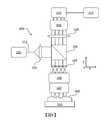
圖1係一系統100之一第一實施例之一圖式,且圖2係使用系統100之量測範圍之一圖式。消除在Z方向上機械掃描工件108。系統100使用一可調諧彩色濾光器來掃過量測範圍且無機械移動。系統100能夠將量測範圍分割成若干關注區域且跳過其中無法找到任何相關資料之部分。系統100可藉由使用即時演算法判定共焦曲線形狀來實現共焦曲線之最佳取樣。此可允許可提供較快度量之較快掃描。FIG. 1 is a diagram of a first embodiment of a
如圖2中所展示,透鏡106及107經設計使得透鏡之焦距依據波長而變化。圖2中之各點對應於由可調諧彩色濾光器選擇之一特定波長帶。可藉由改變自λ1至λn之波長帶來掃描量測範圍以偵測物體所在之位置。As shown in FIG. 2, the
返回至圖1,系統100具有產生一光束111之一寬頻光源101。寬頻光源101之波長可由偵測器110偵測。波長可為可見光、近紅外線、短波紅外線、紫外線或其他波長。Returning to FIG. 1, the
一載物台112經組態以固持一工件108。在一例項中,工件108及/或載物台112固定不移動。工件108可為一半導體晶圓或半導體封裝。A
一可調諧彩色濾光器102定位於光束111之路徑中。可調諧彩色濾光器102經組態以使光束111收窄至一中心波長處之一頻帶。可調諧彩色濾光器102可為一液晶可調諧濾光器、一聲光可調諧濾光器或一可調諧法布裡-珀羅標準具。可調諧彩色濾光器102可包含(諸如)具有液晶之一偏振器。亦可使用改變於不同光學濾光器之間的一機動濾光器輪或其他機構。可調諧彩色濾光器102可為用於一或多個波帶之帶通。A
在一例項中,可調諧彩色濾光器102具有約等於一共焦曲線之一寬度的一頻寬。In one example, the
在一例項中,可調諧彩色濾光器102可定位於寬頻光源101與微透鏡陣列105或分束器104之間的光束111之路徑中。在另一例項中,可調諧彩色濾光器102可安置於微透鏡陣列105與偵測器110之間的光束111之路徑中。在另一特定實施例中,複數個可調諧彩色濾光器102定位於光束111之一路徑中之沿光束111之一路徑之一或多個位置處。In one example, the
一準直透鏡103定位於可調諧彩色濾光器102或寬頻光源101與一微透鏡陣列105之間的光束111之路徑中。準直透鏡103經組態以使光束111變準直而指向微透鏡陣列105。A
一分束器104可定位於可調諧彩色濾光器102與微透鏡陣列105或透鏡系統107之間的光束111之路徑中。A
一微透鏡陣列105定位於光束111之一路徑中。系統100之準確性可取決於微透鏡陣列105之數值孔徑(NA)。微透鏡陣列105之微透鏡之間的間距會影響橫向取樣解析度及串擾量。微透鏡陣列105將光束111聚焦至微透鏡陣列105之一焦平面之複數個點。微透鏡陣列105組態為自載物台112上之工件108反射之光束111之一空間濾光器以藉此僅使聚焦於載物台112上之工件108處之光束111通過。A
一透鏡系統107定位於光束111之一路徑中以使用光束111來使複數個點成像至工件108上。例如,透鏡系統107可為一物鏡。透鏡系統107經組態以提供縱向色差以藉此使不同波長成像於距透鏡系統107之不同距離處。色差可由折射、繞射或折射及繞射兩者之一組合誘發。A
一鏡筒透鏡106可定位於微透鏡陣列105或分束器104與透鏡系統107之間的光束111之一路徑中。在一例項中,鏡筒透鏡106係隨色差繞射。A
自載物台112上之工件108反射之光束111可在由偵測器110接收之前被導引通過微透鏡陣列105。The
一成像透鏡109定位於分束器104與一偵測器110之間的光束之一路徑中。成像透鏡109可使微透鏡陣列105成像至偵測器110上。An
一選用焦點可調諧透鏡可用於系統100中且可定位於鏡筒透鏡106與透鏡系統107之間的光束之一路徑中。可藉由將一焦點可調諧透鏡引入至系統100中來使量測範圍移位於Z方向上且無機械移動。此可用於擴展Z範圍。一電可調諧液體透鏡係一焦點可調諧透鏡之一實例。圖9繪示一組合量測範圍。An optional focus tunable lens can be used in the
一偵測器110經定位以自載物台112上之工件108接收光束111。一偵測器110可為一灰階區域掃描攝影機或其他類型之裝置。偵測器110可量測強度。A
一處理器113可與偵測器110電子通信。處理器113可經組態以判定工件108上之特徵之3D量測。本文中所描述之處理器113、(若干)其他系統或(若干)其他子系統可為包含一個人電腦系統、影像電腦、主機電腦系統、工作站、網路設備、網際網路設備或其他裝置之各種系統之部分。A
處理器113可安置於系統100或另一裝置中或否則為系統100或另一裝置之部分。在一實例中,處理器113可為一獨立控制單元之部分或位於一集中式品質控制單元中。可使用多個處理器113。The
處理器113實際上可由硬體、軟體及韌體之任何組合實施。此外,本文中所描述之其功能可由一個單元執行或分配於不同組件中,該等組件之各者繼而可由硬體、軟體及韌體之任何組合實施。用於實施各種方法及功能之處理器113之程式碼或指令可儲存於可讀儲存媒體(諸如與處理器113電子通信之一電子資料儲存單元中之一記憶體)中。The
處理器113可經組態以使用系統100之輸出或其他輸出來執行諸多功能。例如,處理器113可經組態以將輸出發送至一電子資料儲存單元。處理器113可如本文中所描述般進一步組態。The
可根據本文中所描述之任何實施例來組態處理器113。處理器113亦可經組態以使用系統100之輸出或使用來自其他源之影像或資料來執行其他功能或額外步驟。The
處理器113可依此項技術中已知之任何方式通信耦合至系統100之各種組件或子系統之任何者。此外,處理器113可經組態以藉由可包含有線及/或無線部分之一傳輸媒體來接收及/或獲取來自其他系統之資料或資訊(例如來自諸如一複查工具之一檢測系統的檢測結果、包含設計資料之一遠端資料庫及其類似者)。依此方式,傳輸媒體可充當處理器113與系統100之其他子系統或系統100外之系統之間的一資料鏈路。The
由以下之一或多者實施本文中所揭示之系統100及方法之各種步驟、功能及/或操作:電子電路、邏輯閘、多工器、可程式化邏輯裝置、ASIC、類比或數位控制/開關、微控制器或運算系統。實施諸如本文中所描述之方法之方法的程式指令可經由載體媒體傳輸或儲存於載體媒體上。載體媒體可包含一儲存媒體,諸如一唯讀記憶體、一隨機存取記憶體、一磁碟或光碟、一非揮發性記憶體、一固態記憶體、一磁帶及其類似者。一載體媒體可包含一傳輸媒體,諸如一導線、纜線或無線傳輸鏈路。例如,本發明中所描述之各種步驟可由一單一處理器113或替代地,多個處理器113實施。此外,系統100之不同子系統可包含一或多個運算或邏輯系統。因此,以上描述不應被解譯為限制本發明,而是僅為說明。The various steps, functions and/or operations of the
在一例項中,透過一準直透鏡103來發送來自寬頻光源101之光束111。經準直之光束111照射微透鏡陣列105,微透鏡陣列105將光束111聚焦至微透鏡陣列105之焦平面中之複數個點。複數個點由一透鏡系統107成像至工件108上。由於透鏡系統107之縱向色差,不同波長將成像於距透鏡系統107之不同距離處。In one example, the
系統100不使用寬頻光源101之整個頻寬,而是使用光束111之照明路徑中之一可調諧彩色濾光器102。此可調諧彩色濾光器102可僅允許一選定中心波長處之一窄頻帶通過。在物體側處,此可對應於選擇量測範圍內之一單一Z位準。The
光束111在工件108上反射且反向行進通過透鏡系統107而朝向微透鏡陣列105。微透鏡陣列105現充當一空間濾光器且僅使聚焦於工件108處之光束111通過。因此,僅定位於選定Z位準處之來自工件108之點導致偵測器110上之一信號。The
藉由掃掠自低波長至高波長之窄頻帶,系統100可掃過整個量測範圍且重建工件108之整個表面形貌。By sweeping the narrow frequency band from low wavelength to high wavelength, the
操作不受限於一單一波長範圍。可根據受測試物體之需要來選擇所使用之波長範圍。例如,具有良好反射之物體可使用可見光,低波長可為450 nm,且高波長可為650 nm。帶通如何改變可取決於可調諧彩色濾光器之類型。Operation is not limited to a single wavelength range. The wavelength range used can be selected according to the needs of the tested object. For example, objects with good reflection can use visible light, the low wavelength can be 450 nm, and the high wavelength can be 650 nm. How the bandpass changes may depend on the type of tunable color filter.
在使用系統100之量測期間無需機械移動。無需XY方向移動,因為系統係基於一微透鏡陣列105且一次性擷取一大矩形區域。藉由改變來自可調諧彩色濾光器102之帶通來完成Z方向上之掃描。因為不存在機械移動,所以系統100無振動且具有比先前系統高之產出量。波長之間的切換可在數微秒或數毫秒內完成,其取決於可調諧彩色濾光器102之類型。No mechanical movement is required during the measurement using the
可跳過量測範圍之特定部分。圖3繪示一例示性工件上之量測。例如,可量測圖3中一球柵陣列上之球高。在圖3中,量測範圍內之點指示由可調諧彩色濾光器設定之色彩及所得焦點。此展示範圍A及範圍B內使用多個掃描點。範圍C內不存在掃描點,因為可調諧濾光器使色彩自λA,high即時改變至λB,low。You can skip a specific part of the measurement range. FIG. 3 illustrates an example measurement on an exemplary workpiece. For example, the ball height on a ball grid array in FIG. 3 can be measured. In FIG. 3, the points within the measurement range indicate the color set by the tunable color filter and the resulting focus. In this display range A and B, multiple scan points are used. There is no scan point in the range C, because the tunable filter changes the color from λA,high to λB,low instantly.
可基於標稱球高來選擇圍繞基板之一範圍A及圍繞球頂之一範圍B。A與B之間(即,λA,high與λB,low之間)的範圍C不具有相關資料且可被跳過。可調諧彩色濾光器可依小步進改變波長。接著,波長可自λA,high改變至λB,low。接著,可再次使用小步進來自λB,low變至λB,high。A range A surrounding the substrate and a range B surrounding the top of the ball can be selected based on the nominal ball height. The range C between A and B (ie, between λA, high and λB, low ) has no relevant data and can be skipped. The tunable color filter can change the wavelength in small steps. Then, the wavelength can be changed from λA,high to λB,low . Then, small steps can be used again to change from λB,low to λB,high .
具有一機械Z掃描之先前系統無法跳過量測範圍之部分,因為物體或微透鏡陣列必須自一位置實體移動至另一位置。因此,就一機械掃描而言,無論如何必須掃描範圍C。系統100藉由自範圍A跳躍至範圍B來提供相關資料之較快量測。Previous systems with a mechanical Z-scan cannot skip the part of the measurement range because the object or microlens array must be physically moved from one location to another. Therefore, for a mechanical scan, the range C must be scanned anyway. The
一灰階區域掃描攝影機可用作偵測器110。一波長由可調諧彩色濾光器102選擇。XY解析度及Z解析度彼此獨立,因為不存在多工信號。相互依存之XY解析度及Z解析度亦變得清晰,如圖3中球高量測之實例中所見。A grayscale area scanning camera can be used as the
在先前彩色共焦系統中,物體上之各取樣點(一行像素)保留於感測器上以量測波長。各行中之像素量係XY解析度與Z解析度之間的一折衷。較長行給予較佳Z解析度但較差XY解析度,且反之亦然。波長量測覆蓋全範圍λA,low至λB,high,但在此例項中,經指派以量測波長λA,high至λB,low之像素無用。可使用昂貴高解析度攝影機來得到足夠XY及Z解析度,但未使用諸多像素。此亦造成處理資料時之額外負擔。即使像素不含有用資訊,但亦處理像素。In the previous color confocal system, each sampling point (a row of pixels) on the object remains on the sensor to measure the wavelength. The amount of pixels in each row is a compromise between XY resolution and Z resolution. Longer lines give better Z resolution but worse XY resolution, and vice versa. The wavelength measurement covers the entire range λA,low to λB,high , but in this example, pixels assigned to measure the wavelength λA,high to λB,low are useless. An expensive high-resolution camera can be used to obtain sufficient XY and Z resolution, but many pixels are not used. This also causes an additional burden when processing data. Pixels are processed even if they do not contain useful information.
圖4係一方法200之一流程圖。在201中,使用一寬頻光源來產生一光束。在202中,使用一微透鏡陣列來將光聚焦至微透鏡陣列之一焦平面中之複數個點中。微透鏡陣列組態為一空間濾光器。在203中,使用一可調諧彩色濾光器來使光束收窄至一中心波長處之一頻帶。在204中,使用一透鏡系統來使複數個點成像至一工件上。透鏡系統經組態以提供縱向色差以藉此使不同波長成像於距透鏡系統之不同距離處。在205中,使用微透鏡陣列來使聚焦於工件處之自工件反射之光束通過。在206中,在一偵測器處接收自工件反射之光束。4 is a flowchart of a
方法200可進一步包含使用一處理器來判定工件上特徵之3D量測。3D量測可包含球高、共面性、組件厚度及翹曲之一或多者。在一例項中,方法200進一步包含掃掠自一低波長至一高波長之一窄頻帶且使用處理器來判定工件之一表面形貌。The
可在使用微透鏡陣列來聚焦之前準直光束。The light beam can be collimated before using the microlens array to focus.
可由偵測器偵測僅定位於一選定Z位準處之來自工件之一或多個特徵。如相對於圖3所提及,可使用方法200來跳過工件上之一範圍之部分。One or more features from the workpiece that are only located at a selected Z level can be detected by the detector. As mentioned with respect to FIG. 3, the
儘管圖1中繪示可調諧彩色濾光器102相對於光束111之一路徑位於寬頻光源101與準直透鏡103之間,但可調諧彩色濾光器102可定位於系統100中之其他位置處。例如,可調諧彩色濾光器102可沿光束111之路徑安置於微透鏡陣列105與透鏡系統107之間。Although FIG. 1 shows that the
圖5至圖8係根據本發明之一系統之其他實施例之圖式。此等其他實施例可影響系統之總大小或空間需求。可調諧彩色濾光器102可定位於偵測器110前面之光學路徑中之其他位置處。此不改變系統之功能。在圖5中,系統300將可調諧彩色濾光器102定位於準直透鏡103與分束器104之間的光束111之路徑中。在圖6中,系統400將可調諧彩色濾光器102定位於分束器104與微透鏡陣列105之間的光束111之路徑中。在圖7中,系統500將可調諧彩色濾光器102定位於分束器104與成像透鏡109之間的光束111之路徑中。在圖8中,系統600將可調諧彩色濾光器102定位於成像透鏡109與偵測器110之間的光束111之路徑中。5 to 8 are diagrams of other embodiments of a system according to the present invention. These other embodiments can affect the total size or space requirements of the system. The
亦可在光學路徑中之多個位置處使用一個以上可調諧彩色濾光器102以改良及/或收窄頻寬。因此,系統可包含圖1或圖5至圖8中所展示之位置處之兩個或兩個以上可調諧彩色濾光器102。可藉由使用兩個彩色濾光器來減小通帶之頻寬。一較小頻寬可導致一更準確Z量測。為減小頻寬,一第一濾光器之通帶及一第二濾光器之通帶可重疊,同時具有不同中心波長。例如,第一濾光器可具有10 nm之一頻寬且以500 nm為中心,而第二濾光器可具有10 nm之一頻寬且以505 nm為中心。兩個濾光器之組合可具有以502.5 nm為中心之一5 nm頻寬。More than one
在一實施例中,可使用一隆奇(Ronchi)劃線來代替微透鏡陣列105。隆奇劃線係一平行狹縫群組。若系統係基於微透鏡陣列105,則其可表現得像並行運行之點感測器。若系統係基於一隆奇劃線,則其可表現得像並行運行之線感測器。儘管可發生一略寬共焦曲線,但隆奇劃線可降低成本。In one embodiment, a Ronchi scribe line can be used instead of the
在另一實施例中,可使用一針孔陣列來代替一微透鏡陣列105。In another embodiment, a pinhole array may be used instead of a
儘管已相對於一或多個特定實施例來描述本發明,但應瞭解,可在不背離本發明之範疇之情況下進行本發明之其他實施例。因此,本發明被視為僅受限於隨附申請專利範圍及其合理解譯。Although the invention has been described with respect to one or more specific embodiments, it should be understood that other embodiments of the invention may be made without departing from the scope of the invention. Therefore, the present invention is considered to be limited only by the scope of the accompanying patent application and its comprehensive interpretation.
100:系統101:寬頻光源102:可調諧彩色濾光器103:準直透鏡104:分束器105:微透鏡陣列106:鏡筒透鏡107:透鏡系統108:工件109:成像透鏡110:偵測器111:光束112:載物台113:處理器200:方法201:使用一寬頻光源來產生一光束202:使用一微透鏡陣列來將光聚焦至微透鏡陣列之一焦平面中之複數個點中203:使用一可調諧彩色濾光器來使光束收窄至一中心波長處之一頻帶204:使用一透鏡系統來使複數個點成像至一工件上205:使用微透鏡陣列來使聚焦於工件處之自工件反射之光束通過206:在一偵測器處接收自工件反射之光束300:系統400:系統500:系統600:系統100: System101: Broadband light source102: tunable color filter103: Collimating lens104: beam splitter105: microlens array106: tube lens107: lens system108: artifact109: imaging lens110: Detector111: beam112: stage113: processor200: Method201: Use a broadband light source to generate a beam202: Use a microlens array to focus light into a plurality of points in one focal plane of the microlens array203: Use a tunable color filter to narrow the beam to a band at a central wavelength204: Use a lens system to image multiple points on a workpiece205: Use a microlens array to pass the beam reflected from the workpiece focused on the workpiece206: Receive the beam reflected from the workpiece at a detector300: System400: System500: System600: System
為較完全理解本發明之性質及目的,應參考結合附圖之以下詳細描述,其中:圖1係根據本發明之一系統之一第一實施例之一圖式;圖2係使用圖1之系統之量測範圍之一圖式;圖3繪示一例示性工件上之量測;圖4係根據本發明之一方法之一流程圖;圖5至圖8係根據本發明之一系統之其他實施例之圖式;及圖9繪示一組合量測範圍。For a more complete understanding of the nature and purpose of the present invention, reference should be made to the following detailed description in conjunction with the accompanying drawings, in which:FIG. 1 is a diagram of a first embodiment of a system according to the invention;Figure 2 is a diagram of the measurement range using the system of Figure 1;FIG. 3 shows an example of measurement on an exemplary workpiece;4 is a flowchart of one of the methods according to the present invention;5 to 8 are diagrams of other embodiments of a system according to the present invention; andFIG. 9 illustrates a combined measurement range.
100:系統100: System
101:寬頻光源101: Broadband light source
102:可調諧彩色濾光器102: tunable color filter
103:準直透鏡103: Collimating lens
104:分束器104: beam splitter
105:微透鏡陣列105: microlens array
106:鏡筒透鏡106: tube lens
107:透鏡系統107: lens system
108:工件108: artifact
109:成像透鏡109: imaging lens
110:偵測器110: Detector
111:光束111: beam
112:載物台112: stage
113:處理器113: processor
Claims (18)
Translated fromChineseApplications Claiming Priority (4)
| Application Number | Priority Date | Filing Date | Title |
|---|---|---|---|
| US201862702894P | 2018-07-24 | 2018-07-24 | |
| US62/702,894 | 2018-07-24 | ||
| US16/513,091US10866092B2 (en) | 2018-07-24 | 2019-07-16 | Chromatic confocal area sensor |
| US16/513,091 | 2019-07-16 |
Publications (2)
| Publication Number | Publication Date |
|---|---|
| TW202011124Atrue TW202011124A (en) | 2020-03-16 |
| TWI821338B TWI821338B (en) | 2023-11-11 |
Family
ID=69177890
Family Applications (1)
| Application Number | Title | Priority Date | Filing Date |
|---|---|---|---|
| TW108126097ATWI821338B (en) | 2018-07-24 | 2019-07-24 | 3d measurement systems and methods |
Country Status (13)
| Country | Link |
|---|---|
| US (1) | US10866092B2 (en) |
| EP (1) | EP3807591B1 (en) |
| JP (1) | JP7232895B2 (en) |
| KR (2) | KR20210024675A (en) |
| CN (1) | CN112469961B (en) |
| ES (1) | ES2984587T3 (en) |
| FI (1) | FI3807591T3 (en) |
| MY (1) | MY204178A (en) |
| PH (1) | PH12021550169B1 (en) |
| PT (1) | PT3807591T (en) |
| SG (1) | SG11202100316UA (en) |
| TW (1) | TWI821338B (en) |
| WO (1) | WO2020023427A1 (en) |
Families Citing this family (8)
| Publication number | Priority date | Publication date | Assignee | Title |
|---|---|---|---|---|
| DE102020200214A1 (en)* | 2020-01-09 | 2021-07-15 | Hochschule für angewandte Wissenschaften Kempten Körperschaft des öffentlichen Rechts | Confocal measuring device for 3D measurement of an object surface |
| CN111487038B (en)* | 2020-04-23 | 2022-04-08 | 华侨大学 | Integrated micro-dispersion lens array panel and parallel chromatic confocal measurement system |
| CN112648926B (en)* | 2021-01-13 | 2023-03-28 | 宁波五维检测科技有限公司 | Line-focusing color confocal three-dimensional surface height measuring device and method |
| KR102562630B1 (en)* | 2021-04-13 | 2023-08-02 | 조선대학교산학협력단 | Apparatus of vision chromatic confocal sensor based on a geometrical phase lens |
| DE102022207032A1 (en)* | 2022-07-11 | 2024-01-11 | Micro-Epsilon Optronic Gmbh | Device, device and method for confocal-chromatic distance and/or thickness measurement |
| US12418972B2 (en)* | 2022-09-14 | 2025-09-16 | Kla Corporation | Confocal chromatic metrology for EUV source condition monitoring |
| WO2024261374A1 (en)* | 2023-06-22 | 2024-12-26 | Lmi Technologies Inc. | Optical measurement device and method |
| WO2024261375A1 (en)* | 2023-06-22 | 2024-12-26 | Lmi Technologies Inc. | Optical distance measurement device, optical distance measurement method and use of the optical distance measurement device |
Family Cites Families (23)
| Publication number | Priority date | Publication date | Assignee | Title |
|---|---|---|---|---|
| JPH0526635A (en)* | 1991-07-25 | 1993-02-02 | Sumitomo Cement Co Ltd | Confocal laser scanning microscope for cross section observation |
| US5248876A (en) | 1992-04-21 | 1993-09-28 | International Business Machines Corporation | Tandem linear scanning confocal imaging system with focal volumes at different heights |
| CA2341359A1 (en) | 1998-08-21 | 2000-03-02 | Ian Walton | Novel optical architectures for microvolume laser-scanning cytometers |
| US6724489B2 (en) | 2000-09-22 | 2004-04-20 | Daniel Freifeld | Three dimensional scanning camera |
| DE10242374A1 (en) | 2002-09-12 | 2004-04-01 | Siemens Ag | Confocal distance sensor |
| CN1692296A (en)* | 2002-09-30 | 2005-11-02 | 独立行政法人科学技术振兴机构 | Confocal Microscope and Its Fluorescence Measurement Method and Polarized Light Measurement Method |
| JP2005221451A (en) | 2004-02-09 | 2005-08-18 | Mitsutoyo Corp | Laser displacement gauge |
| JP2006133499A (en) | 2004-11-05 | 2006-05-25 | Shimadzu Corp | Confocal scanner and confocal microscope |
| TWI439684B (en)* | 2005-07-06 | 2014-06-01 | Nanometrics Inc | Photoluminescence imaging with preferential detection of photoluminescence signals emitted from a specified material layer of a wafer or other workpiece |
| DE102005043627B4 (en) | 2005-09-13 | 2012-06-14 | Fraunhofer-Gesellschaft zur Förderung der angewandten Forschung e.V. | Optical sensor and method for optical distance and / or color measurement |
| CN101821659B (en) | 2007-10-11 | 2014-09-24 | 3M创新有限公司 | Chromatic confocal sensor |
| CZ2009133A3 (en)* | 2009-03-03 | 2009-07-08 | Witrins S.R.O. | Measuring device and method for measuring outer dimensions of tested product and use of this device |
| TWI490444B (en)* | 2009-01-23 | 2015-07-01 | Univ Nat Taipei Technology | Slit-scan microscopic system and method using the same |
| DE102012009836A1 (en)* | 2012-05-16 | 2013-11-21 | Carl Zeiss Microscopy Gmbh | Light microscope and method for image acquisition with a light microscope |
| US8654352B1 (en) | 2012-08-08 | 2014-02-18 | Asm Technology Singapore Pte Ltd | Chromatic confocal scanning apparatus |
| US10007109B2 (en)* | 2013-06-20 | 2018-06-26 | The University Of North Carolina At Charlotte | Wavelength discriminating imaging systems and methods |
| DE102013016368B4 (en) | 2013-09-30 | 2024-05-16 | Carl Zeiss Microscopy Gmbh | Light microscope and microscopy method for examining a microscopic sample |
| WO2015177784A2 (en)* | 2014-05-18 | 2015-11-26 | Adom, Advanced Optical Technologies Ltd. | System for tomography and/or topography measurements of a layered object |
| JP6503221B2 (en)* | 2015-05-13 | 2019-04-17 | オリンパス株式会社 | Three-dimensional information acquisition apparatus and three-dimensional information acquisition method |
| US10495446B2 (en)* | 2015-06-29 | 2019-12-03 | Kla-Tencor Corporation | Methods and apparatus for measuring height on a semiconductor wafer |
| DE102016000415A1 (en)* | 2016-01-19 | 2017-07-20 | DüRR DENTAL AG | Device for the three-dimensional detection of a surface structure |
| EP3222965B1 (en)* | 2016-03-25 | 2020-01-15 | Fogale Nanotech | Chromatic confocal device and method for 2d/3d inspection of an object such as a wafer with variable spatial resolution |
| US20190101489A1 (en)* | 2017-09-29 | 2019-04-04 | Michael John Darwin | Method and Apparatus for Simultaneously Measuring 3Dimensional Structures and Spectral Content of Said Structures |
- 2019
- 2019-07-16USUS16/513,091patent/US10866092B2/enactiveActive
- 2019-07-23JPJP2021503834Apatent/JP7232895B2/enactiveActive
- 2019-07-23KRKR1020217005472Apatent/KR20210024675A/ennot_activeCeased
- 2019-07-23WOPCT/US2019/042897patent/WO2020023427A1/ennot_activeCeased
- 2019-07-23KRKR1020237026308Apatent/KR102820242B1/enactiveActive
- 2019-07-23PHPH1/2021/550169Apatent/PH12021550169B1/enunknown
- 2019-07-23SGSG11202100316UApatent/SG11202100316UA/enunknown
- 2019-07-23PTPT198421497Tpatent/PT3807591T/enunknown
- 2019-07-23CNCN201980048978.6Apatent/CN112469961B/enactiveActive
- 2019-07-23MYMYPI2021000247Apatent/MY204178A/enunknown
- 2019-07-23ESES19842149Tpatent/ES2984587T3/enactiveActive
- 2019-07-23FIFIEP19842149.7Tpatent/FI3807591T3/enactive
- 2019-07-23EPEP19842149.7Apatent/EP3807591B1/enactiveActive
- 2019-07-24TWTW108126097Apatent/TWI821338B/enactive
Also Published As
| Publication number | Publication date |
|---|---|
| FI3807591T3 (en) | 2024-08-20 |
| JP2021530714A (en) | 2021-11-11 |
| KR20230119255A (en) | 2023-08-16 |
| KR102820242B1 (en) | 2025-06-12 |
| KR20210024675A (en) | 2021-03-05 |
| US10866092B2 (en) | 2020-12-15 |
| WO2020023427A1 (en) | 2020-01-30 |
| US20200033121A1 (en) | 2020-01-30 |
| CN112469961B (en) | 2022-06-07 |
| SG11202100316UA (en) | 2021-02-25 |
| ES2984587T3 (en) | 2024-10-30 |
| PT3807591T (en) | 2024-08-02 |
| PH12021550169A1 (en) | 2021-10-11 |
| PH12021550169B1 (en) | 2023-01-18 |
| CN112469961A (en) | 2021-03-09 |
| TWI821338B (en) | 2023-11-11 |
| JP7232895B2 (en) | 2023-03-03 |
| EP3807591A4 (en) | 2022-03-16 |
| MY204178A (en) | 2024-08-14 |
| EP3807591B1 (en) | 2024-07-03 |
| EP3807591A1 (en) | 2021-04-21 |
Similar Documents
| Publication | Publication Date | Title |
|---|---|---|
| TWI821338B (en) | 3d measurement systems and methods | |
| TWI484139B (en) | Chromatic confocal scanning apparatus | |
| KR102760925B1 (en) | Inspecting apparatus based on hyper HSI(Hyper Spectral Imaging) | |
| US20180144995A1 (en) | Optical inspection apparatus and method and method of fabricating semiconductor device using the apparatus | |
| TWI835976B (en) | Imaging reflectometer | |
| WO1999064913A1 (en) | Method and system for imaging an object with a plurality of optical beams | |
| US11156566B2 (en) | High sensitivity image-based reflectometry | |
| CN103267482A (en) | High-accuracy displacement detection device and method | |
| US11150078B1 (en) | High sensitivity image-based reflectometry | |
| JP2008215833A (en) | Apparatus and method for measuring optical characteristics | |
| US11898912B2 (en) | Hyperspectral imaging (HSI) apparatus and inspection apparatus including the same | |
| CN203310374U (en) | High precision displacement detection device | |
| US8259297B1 (en) | Scanning focal length metrology | |
| CN210070874U (en) | Super spectral line scanning 3D measuring device | |
| US20250314482A1 (en) | Focus position measurement while scanning | |
| WO2024034067A1 (en) | Sample surface quality management device |