RU2720046C1 - Light-emitting heterostructure with quantum wells of combined profile - Google Patents
Light-emitting heterostructure with quantum wells of combined profileDownload PDFInfo
- Publication number
- RU2720046C1 RU2720046C1RU2019123050ARU2019123050ARU2720046C1RU 2720046 C1RU2720046 C1RU 2720046C1RU 2019123050 ARU2019123050 ARU 2019123050ARU 2019123050 ARU2019123050 ARU 2019123050ARU 2720046 C1RU2720046 C1RU 2720046C1
- Authority
- RU
- Russia
- Prior art keywords
- well
- combined profile
- wells
- quantum
- profile
- Prior art date
Links
Images

Classifications
- H—ELECTRICITY
- H10—SEMICONDUCTOR DEVICES; ELECTRIC SOLID-STATE DEVICES NOT OTHERWISE PROVIDED FOR
- H10H—INORGANIC LIGHT-EMITTING SEMICONDUCTOR DEVICES HAVING POTENTIAL BARRIERS
- H10H20/00—Individual inorganic light-emitting semiconductor devices having potential barriers, e.g. light-emitting diodes [LED]
- H10H20/80—Constructional details
- H10H20/81—Bodies
- H10H20/822—Materials of the light-emitting regions
- H10H20/824—Materials of the light-emitting regions comprising only Group III-V materials, e.g. GaP
- H10H20/825—Materials of the light-emitting regions comprising only Group III-V materials, e.g. GaP containing nitrogen, e.g. GaN
- H—ELECTRICITY
- H10—SEMICONDUCTOR DEVICES; ELECTRIC SOLID-STATE DEVICES NOT OTHERWISE PROVIDED FOR
- H10H—INORGANIC LIGHT-EMITTING SEMICONDUCTOR DEVICES HAVING POTENTIAL BARRIERS
- H10H20/00—Individual inorganic light-emitting semiconductor devices having potential barriers, e.g. light-emitting diodes [LED]
- H10H20/80—Constructional details
- H10H20/81—Bodies
- H10H20/811—Bodies having quantum effect structures or superlattices, e.g. tunnel junctions
Landscapes
- Led Devices (AREA)
Abstract
Description
Translated fromRussianИзобретение относится к конструкции полупроводниковых гетероструктур с квантовыми ямами, применяемых для изготовления источников светового излучения.The invention relates to the construction of semiconductor heterostructures with quantum wells used for the manufacture of light sources.
В настоящее время со стороны разработчиков полупроводниковых приборов большое внимание уделяется поиску альтернативных источников света. Особенно большие успехи в этом направлении достигнуты при использовании в качестве светоизлучающих элементов гетероструктуры с множественными квантовыми ямами (КЯ) на основе барьеров InGaN/GaN. Именно она выступает в качестве светоизлучающего элемента, преобразуя электрический ток в световое излучение. По этой причине от качества изготовления КЯ, ее профиля, геометрических и электрофизических параметров напрямую зависит эффективность будущего источника света.Currently, developers of semiconductor devices pay great attention to the search for alternative light sources. Particularly great successes in this direction were achieved when heterostructures with multiple quantum wells (QWs) based on InGaN / GaN barriers were used as light-emitting elements. It acts as a light-emitting element, converting an electric current into light radiation. For this reason, the efficiency of a future light source directly depends on the quality of manufacture of the QW, its profile, geometric and electrophysical parameters.
Профили КЯ могут быть изготовлены трех типов: прямоугольный, треугольный и параболический. Подавляющее большинство светодиодов на основе гетероструктур из нитридов (InGaN/GaN и им подобные), используемых для изготовления устройств освещения, имеют КЯ прямоугольного профиля. Это обстоятельство объясняется технологической простотой изготовления ямы указанного профиля, а значит и низкой себестоимостью получаемого источника освещения при сравнительно высоком значении внутренней квантовой эффективности.QW profiles can be made of three types: rectangular, triangular and parabolic. The vast majority of LEDs based on nitride heterostructures (InGaN / GaN and the like) used for the manufacture of lighting devices have rectangular QWs. This circumstance is explained by the technological simplicity of manufacturing a pit of the indicated profile, and hence the low cost of the resulting light source with a relatively high value of the internal quantum efficiency.
Однако ямы прямоугольного профиля обладают принципиальным недостатком, который заключается в нерациональном использовании энергетического объема ямы, особенно ярко проявляющийся при малых значениях ее толщины: от 4 нм и меньше. Суть этого недостатка заключается в том, что энергетический зазор между соседними уровнями размерного квантования (УРК) с ростом номера состояния увеличивается по квадратичному закону. Это приводит к высокой плотности УРК у дна КЯ и быстрому уменьшению плотности с ростом номера состояния. Тем самым, верхняя часть КЯ, находящаяся вблизи дна зоны проводимости барьерного слоя, оказывается лишенной разрешенных стационарных состояний для носителей заряда, что снижает вероятность их захвата из зоны проводимости барьерного слоя на состояния КЯ. Следствием низкой скорости захвата свободных носителей на УРК в прямоугольной КЯ является низкая интенсивность генерируемого излучения.However, rectangular-shaped wells have a fundamental drawback, which consists in the irrational use of the energy volume of the well, which is especially pronounced at small values of its thickness: from 4 nm or less. The essence of this drawback is that the energy gap between adjacent levels of dimensional quantization (CRC) with increasing state number increases quadratically. This leads to a high density of the CRC at the bottom of the QW and to a rapid decrease in density with increasing state number. Thus, the upper part of the QW, located near the bottom of the conduction band of the barrier layer, is deprived of allowed stationary states for charge carriers, which reduces the probability of their capture from the conduction band of the barrier layer to the QW states. A consequence of the low capture rate of free carriers on the CRF in a rectangular QW is the low intensity of the generated radiation.
Известна топология квантовой ямы светоизлучающего прибора, содержащая дополнительную яму прямоугольной или треугольной формы [1], создающая ступенчатую структуру, включающую три последовательно выращенных слоя INxGa1-xN с разным содержанием в них индия и устраняющую отрицательное влияние поля спонтанной поляризации в прямоугольной КЯ на скорость излучательной рекомбинации, которое пространственно разделяет отрицательные и положительные заряды, прижимая их к противоположным границам раздела с барьерными слоями. Недостатком аналога является нерациональное использование энергетического объема квантовой ямы, приводящее к низкой эффективности элемента из-за малого уровня инжекции электронов в яму.The topology of a quantum well of a light-emitting device is known, which contains an additional rectangular or triangular well [1], which creates a stepped structure that includes three successively grown layers INx Ga1-x N with different indium contents and eliminates the negative influence of the spontaneous polarization field in a rectangular QW to the rate of radiative recombination, which spatially separates the negative and positive charges, pressing them to opposite interfaces with barrier layers. The disadvantage of the analogue is the irrational use of the energy volume of the quantum well, which leads to low efficiency of the element due to the low level of electron injection into the well.
Известна топология квантовой ямы, представляющая собой прямоугольную КЯ, внутри которой имеется небольшая потенциальная яма, именуемая авторами энергетическим «провалом» [2]. Сформированная таким способом КЯ составного профиля рассматривается как математическая модель для исследования изменения положения уровней размерного квантования (УРК) энергии электронов в собственно КЯ, вызванного наличием потенциального «провала», в зависимости от его ширины и глубины, а также от эффективной массы электронов в провале и в собственно КЯ. Авторами данной модели найден способ определения энергетического положения в КЯ УРК с учетом влияния энергетического «провала». Величина снижения УРК в КЯ зависит от соотношения значений ширины, глубины и эффективных масс электронов в КЯ и провале: чем глубже провал и он шире, тем на большую величину энергии электронные уровни смещаются вниз. Недостатком устройства является не высокая интенсивность излучения, генерируемая светодиодной гетероструктурой типа InGaN/GaN при заданном токе через нее.The topology of a quantum well is known, which is a rectangular QW, inside which there is a small potential well, called by the authors an energy “failure” [2]. The QW of the composite profile formed in this way is considered as a mathematical model for studying the change in the position of the size quantization (CRC) levels of electron energy in the QW itself, caused by the presence of a potential “dip”, depending on its width and depth, as well as on the effective mass of electrons in the dip and in fact QW. The authors of this model have found a way to determine the energy position in the QW of the URC taking into account the influence of the energy “failure”. The magnitude of the decrease in the CRM in the QW depends on the ratio of the width, depth, and effective masses of the electrons in the QW and the dip: the deeper the dip and it is wider, the higher the energy levels shift downward. The disadvantage of this device is the low radiation intensity generated by an InGaN / GaN type LED heterostructure at a given current through it.
Известно техническое решение полупроводникового элемента [3]. В основу данного изобретения положено использование широкозонного соединения AlxGa1-xN переменного состава, генерирующее оптическое излучение в диапазоне длин волн до 280 нм. Недостатком существующих конструкций светоизлучающих элементов на основе алюмоната нитрида галлия является требование внесения высокой концентрации алюминия в GaN для получения барьерных слоев, что приводит к увеличению высоты барьера для дырок на границе с эмиттером дырок, создаваемого встроенным электрическим полем барьера. Это уменьшает эмиссию дырок из эмиттера в активную область, особенно в источниках длин волн менее 380 нм. Подложка полупроводникового элемента изготовлена из сапфира толщиной 500 нм. На ее поверхность нанесен буферный слой AlN из толщиной 20 нм. Эмиттер электронов представляет собой слой Al0.52Ga0.48N толщиной 2 мкм, легированный кремнием с концентрацией 5⋅1018 см-3, Активная область полупроводникового элемента содержит одну или несколько квантовых ям, разделенных барьерными слоями с постоянным составом и только барьерный слой, контактирующий с p-эмиттером, имеет градиентный профиль. Квантовая яма представляет собой слой Al0.48Ga0.52N малой толщины (до 4 нм), а барьерный слой толщиной до 30 нм состоит из многих слоев AlxGa1-xN, каждый из которых имеет толщину 1 нм и процентное содержание алюминия, отличающееся от значения x соседнего слоя, на значение от 2 до 6%.Known technical solution of the semiconductor element [3]. The basis of this invention is the use of a wide-gap compound Alx Ga1-x N of variable composition, generating optical radiation in the wavelength range up to 280 nm. A drawback of existing designs of light-emitting elements based on gallium nitride aluminate is the requirement to introduce a high concentration of aluminum in GaN to obtain barrier layers, which leads to an increase in the height of the barrier for holes at the interface with the hole emitter created by the built-in electric field of the barrier. This reduces the emission of holes from the emitter into the active region, especially in wavelength sources of less than 380 nm. The substrate of the semiconductor element is made of sapphire 500 nm thick. A 20 nm thick AlN buffer layer is deposited on its surface. The electron emitter is an Al0.52 Ga0.48 N layer 2 μm thick, doped with silicon with a concentration of 5 ×18 18 cm-3 . The active region of the semiconductor element contains one or more quantum wells separated by barrier layers with a constant composition and only a barrier layer in contact with p-emitter, has a gradient profile. The quantum well is an Al0.48 Ga0.52 N layer of small thickness (up to 4 nm), and the barrier layer up to 30 nm thick consists of many Alx Ga1-x N layers, each of which has a thickness of 1 nm and a percentage of aluminum that differs from the x value of the adjacent layer, by a value from 2 to 6%.
Недостатком данного технического решения конструкции полупроводникового элемента является нерациональное использование энергетического объема КЯ, приводящего к низкой эффективности элемента из-за малого уровня инжекции электронов в яму.The disadvantage of this technical solution to the design of the semiconductor element is the irrational use of the energy volume of the QW, which leads to low efficiency of the element due to the low level of electron injection into the well.
Известен полупроводниковый светодиодный источник [4] в виде многослойной структуры из полупроводниковых слоев (In,Ga)N. Основой светодиодного источника является подложка, на которой выращиваются полупроводниковые слои с различным содер-жанием In - х и Ga - (1-х) в матрице базового материала GaN. Изменением процентного содержания этих элементов изменятся ширина запрещенной зоны выращиваемого слоя. В результате создаются квантовые ямы (если содержание индия в GaN высокое) или барьерные слои (если вводимое количество индия в растущий слой GaN меньше, чем при выращивании КЯ). Полное число квантовых ямm, участвующих в построении ямы комбинированного профиля, определяется энергетическим зазором между значениями энергии дна зоны проводимости барьерного слоя и дна зоны проводимости квантовой ямы. Последнее задается значением требуемой длины волны генерируемого излучения и может быть значительно больше единицы.Known semiconductor LED source [4] in the form of a multilayer structure of semiconductor layers (In, Ga) N. The basis of the LED source is a substrate on which semiconductor layers with different contents of In - x and Ga - (1-x) in the matrix of the base material GaN are grown. By changing the percentage of these elements, the width of the forbidden zone of the grown layer will change. As a result, quantum wells are created (if the indium content in GaN is high) or barrier layers (if the introduced amount of indium in the growing GaN layer is less than when growing QWs). The total number of quantum wellsm involved in constructing a combined profile well is determined by the energy gap between the energy of the bottom of the conduction band of the barrier layer and the bottom of the conduction band of the quantum well. The latter is set by the value of the required wavelength of the generated radiation and can be significantly larger than unity.
Данное изобретение по существенным признакам является наиболее близким с заявляемым техническим решением и потому выбрано авторами заявляемого технического решения в качестве прототипа.This invention, according to the essential features, is the closest to the claimed technical solution and therefore is selected by the authors of the claimed technical solution as a prototype.
Задачей, на решение которой направлено предлагаемое решение, является увеличение интенсивности излучения, генерируемого светодиодной гетероструктурой типа InGaN/GaNПрИзаданном токе через нее.The problem to be solved by the proposed solution is to increase the intensity of the radiation generated by the LED heterostructure InGaN / GaN p-typeandn given current therethrough.
Поставленная задача решается тем, что в светодиодной гетероструктуре с КЯ, содержащей подложку из сапфира, с нанесенными на ней последовательно буферным слоем, выполненным из нелегированного GaN, n-эмиттерным слоем, выполненным в виде слоя GaN, легированного кремнием, и p-эмиттерный слой GaN, легированный магнием, активная область, расположенная между n-эмиттерным и p-эмиттерным слоями, состоит из нескольких квантовых ям, каждая из которых имеет комбинированный профиль, полученный последовательным нанесением пяти слоев InxGa1-xN, образующих последовательность вида:The problem is solved in that in a LED heterostructure with a QW containing a sapphire substrate, sequentially deposited on it with a buffer layer made of undoped GaN, an n-emitter layer made in the form of a silicon doped GaN layer, and a GaN p-emitter layer doped with Mg, an active region disposed between the n-p-emitter and emitter layers composed of multiple quantum wells, each having a combined profile obtained by applying successive layers of five inx Ga1-x N, is formed after sequence kind:

члены которой отличаются друг от друга процентным содержанием индия в соседних слоях: х1, х2, x3, х2, х1 так, что xi=x1qi-1, где i=2, 3 и q>1, а также тем, что толщина каждой последующей ямыak, k=2, 3 увеличивается по сравнению с толщиной предыдущей ямыak-1 на постоянную величину р>1, являющуюся множителем геометрической прогрессииak=ak-1⋅p. Изготавливаемая таким способом КЯ комбинированного профиля отделяется от других ям того же профиля барьерным слоем из GaN.whose members differ from each other by the percentage of indium in neighboring layers: x1 , x2 , x3 , x2 , x1 so that xi = x1 qi-1 , where i = 2, 3 and q> 1 , as well as the fact that the thickness of each subsequent wellak , k = 2, 3 increases compared with the thickness of the previous wellak-1 by a constant value p> 1, which is a geometric progression factorak =ak-1 ⋅p. A QW of a combined profile produced in this way is separated from other wells of the same profile by a GaN barrier layer.
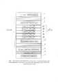
На фиг. 1 приведена конструкция светодиодной гетероструктуры с тремя квантовыми ямами комбинированного профиля, каждая из которых образована последовательным нанесением пяти слоев.In FIG. Figure 1 shows the design of an LED heterostructure with three quantum wells of a combined profile, each of which is formed by sequential deposition of five layers.
На фиг. 2 представлена энергетическая диаграмма КЯ комбинированного профиля для случая комбинирования ямы из трех прямоугольных ям.In FIG. Figure 2 shows the energy diagram of the QW of a combined profile for the case of combining a well from three rectangular wells.
Светодиодная гетероструктура с тремя квантовыми ямами комбинированного профиля, приведенная на фиг. 1, включает следующие слои:The LED heterostructure with three quantum wells of a combined profile shown in FIG. 1 includes the following layers:
1 - подложка из сапфира ориентацией (0001), SiC, ZnO или других материалов;1 - a sapphire substrate with the (0001) orientation, SiC, ZnO or other materials;
2 - буферный слой из нелегированного GaN (концентрация носителей - 8⋅1016 см-3), наносимый для уменьшения плотности дислокаций в выращиваемых далее слоях;2 - buffer layer of undoped GaN (carrier concentration - 8⋅1016 cm-3 ), applied to reduce the density of dislocations in the layers grown further;
3 - n-эмиттерный слой из n-GaN, легированный кремнием с концентрацией Nd=2-6⋅1018 см-3;3 - n-emitter layer of n-GaN doped with silicon with a concentration of Nd = 2-6⋅1018 cm-3 ;
4 - квантовые ямы разной ширины комбинированного профиля, состоящие из пяти слоев прямоугольного профиля (41)-(45), выполненных из
5 - барьерные слои из широкозонного GaN толщиной 15-30 нм;5 - barrier layers of wide-gap GaN with a thickness of 15-30 nm;
6 - p-эмиттерный слой из p-GaN, легированный магнием с концентрацией Na=2-6⋅1017 см-3.6 - p-emitter p-GaN layer doped with magnesium with a concentration of Na = 2-6⋅1017 cm-3 .
Повышение уровня инжекции электронов в квантовую яму комбинированного профиля достигается увеличением плотности УРК в верхней части энергетического объема КЯ. Это достигается изготовлением КЯ в виде совокупности прямоугольных ям различной толщины, размещенных одна над другой подобно «воронке», т.е. соосно относительно друг друга. Толщина каждой последующей КЯ увеличивается по определенному закону по мере увеличения ее энергетического положения в яме комбинированного профиля. Число комбинируемых ям может быть равно двум и более. Оно определяется величиной энергетического зазора между дном зоны проводимости барьерного слоя и дном зоны проводимости КЯ минимальной толщины. При этом каждая прямоугольная яма имеет энергетическую глубину, необходимую для размещения в ней двух УРК.An increase in the level of electron injection into the quantum well of the combined profile is achieved by increasing the CRF density in the upper part of the QW energy volume. This is achieved by manufacturing QWs in the form of a set of rectangular pits of various thicknesses, placed one above the other like a “funnel”, i.e. coaxially relative to each other. The thickness of each subsequent QW increases according to a certain law as its energy position in the pit of the combined profile increases. The number of combined pits may be two or more. It is determined by the magnitude of the energy gap between the bottom of the conduction band of the barrier layer and the bottom of the conduction band of the QW of the minimum thickness. In addition, each rectangular pit has the energy depth necessary to place two URC in it.
Энергетическая диаграмма КЯ комбинированного профиля для случая комбинирования ямы из трех прямоугольных ям представлен на фиг. 2. Результирующий энергетический спектр комбинированной ямы содержит шесть УРК: по два уровня в трех объединяемых ямах прямоугольного профиля. Положительным результатом предлагаемой конструкции КЯ является увеличение числа УРК в яме заданной глубины и, что особенно важно, в верхней части энергетического спектра ямы. Следствием это является повышение интенсивности излучения гетероструктуры по сравнению с гетероструктурой, использующей одиночную КЯ прямоугольного профиля. Физическая причина повышения интенсивности излучения квантовой ямой комбинированного профиля заключается в увеличении числа неравновесных носителей заряда, захватываемых электронной и дырочной КЯ и участвующих в излучательной рекомбинации. Эффект увеличения интенсивности излучения физически объясняется следующим образом.The energy diagram of the QW of the combined profile for the case of combining a well of three rectangular wells is shown in FIG. 2. The resulting energy spectrum of the combined well contains six URC: two levels in three combined wells of a rectangular profile. A positive result of the proposed QW design is an increase in the number of CRF in the well of a given depth and, most importantly, in the upper part of the energy spectrum of the well. This results in an increase in the radiation intensity of the heterostructure as compared with a heterostructure using a single QW of a rectangular profile. The physical reason for the increase in the radiation intensity by the quantum well of the combined profile is an increase in the number of nonequilibrium charge carriers captured by the electron and hole QWs and participating in radiative recombination. The effect of increasing the radiation intensity is physically explained as follows.
Полный ток, протекающий через гетероструктуру можно разделить на две составляющих: ток инжекции и сквозной ток. Первый ток образуют носители заряда, которые захватываются КЯ и рекомбинируют в ней с излучением квантов света. Второй ток создается носителями, которые пролетают через гетероструктуру без излучательной рекомбинации, т.е. это носители, не захватываемые ямами вообще или захватываемые, но быстро эмитируемые ямами в барьерные слои без рекомбинации. У выпускаемых в настоящее время светодиодных источников их соотношение не превышает 1:10. Увеличение интенсивности излучения света в ямах комбинированного профиля происходит за счет увеличения первой составляющей тока, вызванного уменьшением второй составляющей, которое, в свою очередь, вызвано увеличением скорости захвата носителей заряда из зоны проводимости барьерного слоя на состояния комбинированной КЯ. К увеличению скорости захвата приводит создание «мелких» УРК, облегчающих захват, из-за использования ям большей толщины и ширины их запрещенной зоны по сравнению с требуемыми для генерации заданного излучения.The total current flowing through the heterostructure can be divided into two components: injection current and through current. The first current is formed by charge carriers that are captured by the QW and recombine in it with the emission of light quanta. The second current is created by carriers that fly through the heterostructure without radiative recombination, i.e. these are carriers that are not trapped by the pits at all or trapped, but are quickly emitted by the pits into the barrier layers without recombination. For currently produced LED sources, their ratio does not exceed 1:10. An increase in the intensity of light emission in the wells of the combined profile occurs due to an increase in the first component of the current caused by a decrease in the second component, which, in turn, is caused by an increase in the rate of capture of charge carriers from the conduction band of the barrier layer to the states of the combined QW. An increase in the capture rate is caused by the creation of “shallow” URCs, which facilitate capture, due to the use of pits with a greater thickness and width of their forbidden zone than those required to generate a given radiation.
Важными обстоятельствами, характеризующими комбинированный профиль ямы, являются следующие:Important circumstances characterizing the combined pit profile are as follows:
- увеличение толщины комбинируемых ям по закону геометрической прогрессии. Толщина первой КЯ задается генерируемой длиной волны, а знаменатель прогрессии определяется производителем по желаемой крутизне комбинированного профиля ямы-воронки. Предпочтительное значение знаменателя прогрессии: 1<q<2;- an increase in the thickness of the combined pits according to the law of geometric progression. The thickness of the first QW is determined by the generated wavelength, and the denominator of the progression is determined by the manufacturer according to the desired slope of the combined profile of the funnel pit. The preferred value of the denominator of progression: 1 <q <2;
- увеличение ширины запрещенной зоны наносимых КЯ за счет изменения процентного содержания индия х в составе вещества, используемого для роста комбинируемых прямоугольных ям InxGa1-xN, по закону- an increase in the band gap of the applied QWs due to a change in the percentage of indium x in the composition of the substance used for the growth of combined rectangular Inx Ga1-x N wells, according to the law

- каждая из участвующих в комбинировании профиля прямоугольная КЯ должна иметь число УРК, равное двум.- each of the rectangular QWs participating in the combination of the profile should have a CRM number equal to two.
Оценим величину выигрыша в интенсивности, генерируемой КЯ комбинированного профиля, по сравнению с гетероструктурой с одиночной КЯ прямоугольного профиля.Let us estimate the gain in the intensity generated by the QW of the combined profile in comparison with the heterostructure with a single QW of a rectangular profile.
Максимальное значение интенсивности генерируемого излучения гетероструктурой с КЯ определяется суммой интенсивностей от отдельных ям. Если в гетероструктуре находится одинаковое число КЯ, равное M, для электронов и для дырок с плотностью электронных состояний в них

Здесь Br - вероятность излучательной рекомбинации электронов из n-КЯ и дырок из р-КЯ толщинойа; n2D(E) - плотность энергетических состояний в электронной и дырочной КЯ [1];


Из выражения (2) следует, что интенсивность излучения гетероструктуры с одиночными КЯ тем больше, чем больше толщина КЯа, больше их число М и число УРК в каждой из электронных N и дырочных Р ямах.It follows from expression (2) that the radiation intensity of a heterostructure with single QWs is greater, the larger the QW thicknessa , the greater their number M and the number of CRCs in each of the electron N and hole P wells.
Энергетические возможности комбинированной ямы на примере комбинирования трех прямоугольных КЯ можно оценить с помощью выражения (2), которое для случая комбинации электронных и дырочных ям примет вид:The energy capabilities of a combined well using the example of combining three rectangular QWs can be estimated using expression (2), which for the combination of electron and hole wells will take the form:

где обозначено: N1, N2, N3 - количество УРК в ямах для электронов; P1, P2. Р3 - количество УРК в нижней и двух верхних ямах для дырок; М - число КЯ с комбинированным профилем в гетероструктуре. Тогда из выражения (3) найдем:where it is indicated: N1 , N2 , N3 - the number of URC in the wells for electrons; P1 , P2 . P3 - the number of URC in the lower and two upper holes for holes; M is the number of QWs with a combined profile in the heterostructure. Then from the expression (3) we find:

Сравнивая интенсивности двух гетероструктур с КЯ различного профиля с использованием выражения (2), получим:Comparing the intensities of two heterostructures with QWs of different profiles using expression (2), we obtain:

Можно видеть, что КЯ комбинированного профиля способна обеспечить значительный выигрыш в интенсивности излучения для q>1. Отношение числа уровней для дырок в узкой и широких р-КЯ нами не подсчитывалось, но с точностью, достаточной для оценки возможностей ям с комбинированным профилем, их число можно взять равными значениям, найденным для n-КЯ: P3=N3, P2=N2, P1=Nl.It can be seen that the QW of the combined profile is capable of providing a significant gain in the radiation intensity for q> 1. We did not calculate the ratio of the number of levels for holes in narrow and wide p-QWs, but with an accuracy sufficient to assess the capabilities of wells with a combined profile, their number can be taken equal to the values found for n-QWs: P3 = N3 , P2 = N2 , P1 = Nl .
Пример:Example:
Основным параметром, задающим число УРК в комбинируемых КЯ, является ширина первой ямы. Если по длине волны требуемого излучения получаемое значение ширины этой ямы будет малым, то число УРК может оказаться равным единице из-за большого значения его энергии активации первого уровня -
Опыт проведения расчетов по определению энергетического положения УРК в ямах показывает, что в случае составного профиля из прямоугольных ям верхней уровень энергии нижней ямы


Здесь ΔEc выражено в эВ. Пользуясь приведенной записью условия наличия в яме k уровней квантования, найдем толщину нижней ямы, при которой в яме будет один и два УРК, обеспечивающих возможность комбинирования нескольких прямоугольных КЯ:Here ΔEc is expressed in eV. Using the above record of the condition for the presence of k quantization levels in the well, we find the thickness of the lower well at which there will be one and two URCs in the well, providing the possibility of combining several rectangular QWs:

Здесь обозначено: h=6.62⋅10-34 Дж⋅с - постоянная Планка. Тогда для случая одного уровня k=1 выражение (5) дает

Используя приведенные выше рассуждения, из выражения (6) найдем толщину нижней (первой) квантовой ямы:Using the above reasoning, from expression (6) we find the thickness of the lower (first) quantum well:

Количество требуемых для комбинирования профиля прямоугольных ям найдем из следующего рассмотрения.The number of rectangular pits required for combining the profile is found from the following consideration.
Толщины всех ям не должны превышать длину волны де Бройля, но каждая выше лежащая яма делается толще предыдущей. Тогда в верхних ямах расстояние между ее УРК будет в кратное число раз меньше, чем в нижней. Так, при двукратном увеличении расстояния между ее уровнями будет в четыре раза меньше, чем у нижней ямы. Этим обеспечится дополнительное уплотнение уровней энергии в яме комбинированного профиля, а значит и числа рекомбинируемых носителей заряда.The thicknesses of all the holes should not exceed the de Broglie wavelength, but each higher lying hole is thicker than the previous one. Then, in the upper pits, the distance between its URC will be a multiple times smaller than in the lower. So, with a twofold increase in the distance between its levels, it will be four times less than that of the lower pit. This will provide additional densification of energy levels in the well of the combined profile, and hence the number of recombined charge carriers.
Количество комбинируемых ям зависит от общей глубиной ямы, определяемой как разность энергий дна зоны проводимости вещества барьерного слоя и вещества ямы:

Здесь е=1.6⋅10-19 Кл. Поскольку в (6) значения толщины вышележащих ям больше значения толщины нижней, первой ямы, то стоящие в круглых скобках дроби образуют убывающую геометрическую прогрессию, в которой каждая последующая яма будет иметь толщинуak меньше толщины предыдущей ямыak-1 в определенное число q раз:ak=ak-1⋅q. Число q задается разработчиком и может быть любым, но больше единицы. Так, если значения толщины увеличиваются, например, в 1.7 раза, то соседние слагаемые в (6) будут отличаться на множитель q2=1.72=2.89, и прогрессия будет быстро сходящейся. Это позволяет переписать выражение (6) в виде:Here e = 1.6⋅10-19 Cl. Since in (6) the values of the thickness of the overlying pits are greater than the thickness of the lower, first pit, fractions in parentheses form a decreasing geometric progression in which each subsequent pit will have a thicknessak less than the thickness of the previous pitak-1 by a certain number q times:ak =ak-1 ⋅q. The number q is set by the developer and can be any, but greater than one. So, if the thickness values increase, for example, 1.7 times, then the adjacent terms in (6) will differ by a factor q2 = 1.72 = 2.89, and the progression will quickly converge. This allows you to rewrite expression (6) as:

Здесь m - число КЯ, задействованных для формирования ямы комбинированного профиля. Второе слагаемое в правой части (5) описывает энергетический интервал величиной в один квант теплового колебания решетки между соседними объединяемыми ямами. Подставив в (5) значение знаменателя прогрессии, получимHere, m is the number of QWs involved in the formation of a pit of a combined profile. The second term in the right-hand side of (5) describes the energy interval of one quantum of the thermal vibration of the lattice between adjacent combined wells. Substituting in (5) the value of the denominator of the progression, we obtain

Из выражения (8) можно видеть, что сумму прогрессии с точностью до 2-3 процентов обеспечат всего лишь три первых слагаемых, сумма которых равна 5.9. Это означает, что в рассмотренном примере КЯ комбинированного профиля можно составить из трех прямоугольных ям, толщины которых соотносятся кака1 :а2 :a3 = 1,00 : 1.70 : 2.89.From expression (8), it can be seen that the sum of the progression with an accuracy of 2-3% will be provided by only the first three terms, the sum of which is 5.9. This means that in the considered example, the QW of the combined profile can be composed of three rectangular wells, the thicknesses of which are correlated asa1 :a2 :a3 = 1.00: 1.70: 2.89.
Тогда значения толщины второй и третьей КЯ получим умножением толщины первой ямы на знаменатель прогрессии в первой и во второй степени соответственно:а2=1.7⋅4.5=7.7 нм,а3=1.7⋅7.7=13.1 нм.Then, the thickness values of the second and third QWs will be obtained by multiplying the thickness of the first well by the denominator of the progression in the first and second degree, respectively:а2 = 1.7⋅4.5 = 7.7 nm,and3 = 1.7⋅7.7 = 13.1 nm.
Энергии УРК в каждой из этих КЯ, получаемых на барьерах InxGa1-xN/GaN с разной шириной ямы, рассчитываются по выражениюThe energies of the CRC in each of these QWs obtained on Inx Ga1-x N / GaN barriers with different well widths are calculated by the expression

Первая квантовая яма толщиной
Вторая квантовая яма толщиной

Третья квантовая яма толщиной

Энергетическая диаграмма КЯ комбинированного профиля для выбранного примера приведена на фигуре 2. В проведенном расчете энергий УРК в ямах разной толщины молчаливо предполагалось, что суммарный энергетический спектр аддитивно складывается из трех спектров: спектра нижней КЯ, на который накладываются спектры второй и третьей ям. Эти спектры при объединении квантовых ям никак не меняются, не зависят друг от друга. Это предположение является довольно грубым, т.к. физически взаимодействие ям существует и может оказаться сильным. Однако оно не изменяет главной сути предлагаемого технического решения. Уточнение модели можно провести с использованием расчета спектра прямоугольной КЯ с «потенциальным провалом» в терминологии авторов [2].The energy diagram of the QW of the combined profile for the selected example is shown in Fig. 2. In the calculation of the energies of the CRC in wells of different thicknesses, it was tacitly assumed that the total energy spectrum additively consists of three spectra: the spectrum of the lower QW, on which the spectra of the second and third wells are superimposed. When combining quantum wells, these spectra do not change at all, do not depend on each other. This assumption is rather crude, because physically, the interaction of the pits exists and can be strong. However, it does not change the main essence of the proposed technical solution. The model refinement can be carried out using the calculation of the spectrum of a rectangular QW with a “potential dip” in the terminology of the authors [2].
В действительности энергетический спектр комбинированной КЯ (ККЯ), полученной объединением нескольких прямоугольных ям не будет суммой объединяемых ям из-за их взаимодействия. Вдали от линии объединения ям спектр ККЯ будет мало отличаться от спектра соответствующей КЯ, тогда как вблизи линии изменения будут максимальны вплоть до исчезновения отдельных уровней размерного квантования. Точный расчет спектра ПКЯ можно провести с использованием модели ямы с потенциальным «провалом» [2].In fact, the energy spectrum of a combined QW (QW) obtained by combining several rectangular wells will not be the sum of the combined wells due to their interaction. Far from the merging line of the wells, the QW spectrum will differ little from the spectrum of the corresponding QW, while near the line of variation, the maximum will be up to the disappearance of individual levels of dimensional quantization. An accurate calculation of the PCW spectrum can be carried out using a well model with a potential “dip” [2].
Сравним интенсивности излучения одиночной ямы и ямы комбинированным профилем, составленным из трех прямоугольных ям. Обозначив R3=N3/N1=P3/N1 и R2=N2/Nl=P2/Nl, из (4) найдемLet us compare the radiation intensities of a single well and a well with a combined profile composed of three rectangular wells. Denoting R3 = N3 / N1 = P3 / N1 and R2 = N2 / Nl = P2 / Nl , from (4) we find

Поскольку во всех участвующих в комбинировании КЯ число уровней должно быть равным двум, то число возможных переходов между электронными и дырочными уровнями будет равно 36. Тогда выигрыш в интенсивности генерируемого излучения составитSince the number of levels in all QWs participating in the combination should be equal to two, the number of possible transitions between the electron and hole levels will be 36. Then the gain in the intensity of the generated radiation will be

В действительности число излучательных переходов будет меньше указанного выше ввиду преимущественно безизлучательной релаксации носителей заряда с верхних уровней энергии на нижние. Из физических соображений и модельных представлений о возможных схемах рекомбинации следует, что наиболее вероятными излучательными переходами будут переходы между низшими уровнями энергии: электроны с первого уровня нижней n-КЯ будут рекомбинировать с излучением кванта света с дырками первого УРК узкой p-КЯ. Перекрестные переходы вида «узкая n-КЯ - широкая р-КЯ» и «широкая n-КЯ - узкая р-КЯ», а также переходы вида «широкая n-КЯ - широкая р-КЯ» маловероятны.In fact, the number of radiative transitions will be less than the one indicated above due to the predominantly nonradiative relaxation of charge carriers from upper energy levels to lower. From physical considerations and model ideas about possible recombination schemes, it follows that the most probable radiative transitions will be the transitions between the lower energy levels: the electrons from the first level of the lower n-QW will recombine with the radiation of a quantum of light with holes of the first CRF of a narrow p-QW. Cross transitions of the form "narrow n-QW - wide r-QW" and "wide n-QW - narrow r-QW", as well as transitions of the form "wide n-QW - wide r-QW" are unlikely.
Следовательно, для получения оценки возможного выигрыша в интенсивности излучения от применения ям комбинированного профиля, приближенной к реальной ситуации, воспользуемся выражением (4), оставив нем только первое слагаемое правой части при R2=1. Тогда получим
Таким образом, численные расчеты показывают, что выигрыш в интенсивности излучения светодиодной гетероструктуры с квантовыми ямами комбинированного профиля, составленной из трех ям, в сравнении с гетероструктурами, в которых квантовые ямы имеют прямоугольный профиль, при той же глубине квантовых ям что и в случае гетероструктур с ямами комбинированного профиля, может достигать более 25 раз при одинаковом значении сквозного тока через источник излучения.Thus, numerical calculations show that the gain in the radiation intensity of a LED heterostructure with a quantum well of a combined profile composed of three wells, compared with heterostructures in which quantum wells have a rectangular profile, with the same depth of quantum wells as in the case of heterostructures with pits of a combined profile, can reach more than 25 times with the same value of the through current through the radiation source.
Источники информации, использованные при составлении описания изобретения:Sources of information used in the preparation of the description of the invention:
1. Approaches for high internal quantum efficiency green InGaN light-emitting diodes with large overlap quantum wells». Optics Express. 2011. - V. 19. - No. S4. - A 991.1. Approaches for high internal quantum efficiency green InGaN light-emitting diodes with large overlap quantum wells. " Optics Express. 2011. - V. 19. - No. S4. - A 991.
2. Драгунов В.П, Гридчин B.A., Неизвестный И.Г. Основы наноэлектроники: учебное пособие. 2-е изд. - М.: Логос, 2006. - 496 с.2. Dragunov V.P., Gridchin B.A., Unknown I.G. Fundamentals of Nanoelectronics: a training manual. 2nd ed. - M .: Logos, 2006 .-- 496 p.
3. RU 2262155 С1. H01L 33/00 (2000/013) / Авторы: Карпов С.Ю., Мымрин В.Ф. «Полупроводниковый элемент, излучающий свет в ультрафиолетовом диапазоне». Патентообладатель - Закрытое акционерное общество «Нитридные источники света» (RU)/ Заявка 200412877.28 от 14.09.2004.3. RU 2262155 C1. H01L 33/00 (2000/013) / Authors: Karpov S.Yu., Mymrin V.F. "The semiconductor element that emits light in the ultraviolet range." Patent holder - Closed Joint-Stock Company Nitride Light Sources (RU) / Application 200412877.28 of September 14, 2004.
4. United States Patent Hooper et al. Patent No US 7.115.167 B2 «Method of growing a semiconductor multi-layer structure@ Date of Patent: Oct. 3. 2006. (Прототип).4. United States Patent Hooper et al. Patent No US 7.115.167 B2 “Method of growing a semiconductor multi-layer structure @ Date of Patent: Oct. 3.2006. (Prototype).
Claims (3)
Translated fromRussian
Priority Applications (1)
| Application Number | Priority Date | Filing Date | Title |
|---|---|---|---|
| RU2019123050ARU2720046C1 (en) | 2019-07-17 | 2019-07-17 | Light-emitting heterostructure with quantum wells of combined profile |
Applications Claiming Priority (1)
| Application Number | Priority Date | Filing Date | Title |
|---|---|---|---|
| RU2019123050ARU2720046C1 (en) | 2019-07-17 | 2019-07-17 | Light-emitting heterostructure with quantum wells of combined profile |
Publications (1)
| Publication Number | Publication Date |
|---|---|
| RU2720046C1true RU2720046C1 (en) | 2020-04-23 |
Family
ID=70415451
Family Applications (1)
| Application Number | Title | Priority Date | Filing Date |
|---|---|---|---|
| RU2019123050ARU2720046C1 (en) | 2019-07-17 | 2019-07-17 | Light-emitting heterostructure with quantum wells of combined profile |
Country Status (1)
| Country | Link |
|---|---|
| RU (1) | RU2720046C1 (en) |
Cited By (1)
| Publication number | Priority date | Publication date | Assignee | Title |
|---|---|---|---|---|
| CN115377259A (en)* | 2022-10-26 | 2022-11-22 | 江西兆驰半导体有限公司 | Light emitting diode epitaxial wafer, preparation method thereof and light emitting diode |
Citations (9)
| Publication number | Priority date | Publication date | Assignee | Title |
|---|---|---|---|---|
| US715167A (en)* | 1902-06-04 | 1902-12-02 | John Alex Snavely | Hydraulic ram. |
| WO2001037351A1 (en)* | 1999-11-19 | 2001-05-25 | Cree Lighting Company | Multi color solid state led/laser |
| RU2262156C1 (en)* | 2004-09-14 | 2005-10-10 | Закрытое акционерное общество "Нитридные источники света" | Semiconductor element emitting light in ultraviolet range |
| US7115167B2 (en)* | 2001-02-23 | 2006-10-03 | Sharp Kabushiki Kaisha | Method of growing a semiconductor multi-layer structure |
| US7362048B2 (en)* | 1996-07-29 | 2008-04-22 | Nichia Kagaku Kogyo Kabushiki Kaisha | Light emitting device with blue light led and phosphor components |
| RU83655U1 (en)* | 2008-06-26 | 2009-06-10 | Общество с ограниченной ответственностью "Эпи-Тех" | LED HETEROSTRUCTURE WITH MULTIPLE INGAN / GAN QUANTUM PITS |
| US7709284B2 (en)* | 2006-08-16 | 2010-05-04 | The Regents Of The University Of California | Method for deposition of magnesium doped (Al, In, Ga, B)N layers |
| US8044381B2 (en)* | 2007-07-30 | 2011-10-25 | Hewlett-Packard Development Company, L.P. | Light emitting diode (LED) |
| RU119165U1 (en)* | 2012-04-03 | 2012-08-10 | Федеральное государственное бюджетное учреждение науки Научно-технологический центр микроэлектроники и субмикронных гетероструктур Российской академии наук (НТЦ микроэлектроники РАН) | SEMICONDUCTOR RADIATING HETEROSTRUCTURE (OPTIONS) |
- 2019
- 2019-07-17RURU2019123050Apatent/RU2720046C1/enactive
Patent Citations (9)
| Publication number | Priority date | Publication date | Assignee | Title |
|---|---|---|---|---|
| US715167A (en)* | 1902-06-04 | 1902-12-02 | John Alex Snavely | Hydraulic ram. |
| US7362048B2 (en)* | 1996-07-29 | 2008-04-22 | Nichia Kagaku Kogyo Kabushiki Kaisha | Light emitting device with blue light led and phosphor components |
| WO2001037351A1 (en)* | 1999-11-19 | 2001-05-25 | Cree Lighting Company | Multi color solid state led/laser |
| US7115167B2 (en)* | 2001-02-23 | 2006-10-03 | Sharp Kabushiki Kaisha | Method of growing a semiconductor multi-layer structure |
| RU2262156C1 (en)* | 2004-09-14 | 2005-10-10 | Закрытое акционерное общество "Нитридные источники света" | Semiconductor element emitting light in ultraviolet range |
| US7709284B2 (en)* | 2006-08-16 | 2010-05-04 | The Regents Of The University Of California | Method for deposition of magnesium doped (Al, In, Ga, B)N layers |
| US8044381B2 (en)* | 2007-07-30 | 2011-10-25 | Hewlett-Packard Development Company, L.P. | Light emitting diode (LED) |
| RU83655U1 (en)* | 2008-06-26 | 2009-06-10 | Общество с ограниченной ответственностью "Эпи-Тех" | LED HETEROSTRUCTURE WITH MULTIPLE INGAN / GAN QUANTUM PITS |
| RU119165U1 (en)* | 2012-04-03 | 2012-08-10 | Федеральное государственное бюджетное учреждение науки Научно-технологический центр микроэлектроники и субмикронных гетероструктур Российской академии наук (НТЦ микроэлектроники РАН) | SEMICONDUCTOR RADIATING HETEROSTRUCTURE (OPTIONS) |
Cited By (1)
| Publication number | Priority date | Publication date | Assignee | Title |
|---|---|---|---|---|
| CN115377259A (en)* | 2022-10-26 | 2022-11-22 | 江西兆驰半导体有限公司 | Light emitting diode epitaxial wafer, preparation method thereof and light emitting diode |
Similar Documents
| Publication | Publication Date | Title |
|---|---|---|
| Pope et al. | Carrier leakage in InGaN quantum well light-emitting diodes emitting at 480 nm | |
| TWI436495B (en) | Nitride-based illuminating device | |
| JP5737111B2 (en) | Group III nitride semiconductor light emitting device | |
| TWI403002B (en) | Semiconductor light-emitting element | |
| US9397258B2 (en) | Semiconductor structures having active regions comprising InGaN, methods of forming such semiconductor structures, and light emitting devices formed from such semiconductor structures | |
| US9634182B2 (en) | Semiconductor structures having active regions including indium gallium nitride, methods of forming such semiconductor structures, and related light emitting devices | |
| US20130270519A1 (en) | Non-Uniform Multiple Quantum Well Structure | |
| US20140225059A1 (en) | LED with Improved Injection Efficiency | |
| US9343626B2 (en) | Semiconductor structures having active regions comprising InGaN, methods of forming such semiconductor structures, and light emitting devices formed from such semiconductor structures | |
| JP2010532926A (en) | Radiation emitting semiconductor body | |
| JP2020521312A (en) | Semiconductor device and semiconductor device package including the same | |
| JP2014525682A (en) | Optoelectronic parts | |
| US20160276537A1 (en) | Light-emitting device and production method therefor | |
| RU2719339C1 (en) | Method of producing nitride semiconductor emitting ultraviolet radiation element and nitride semiconductor emitting ultraviolet radiation element | |
| KR100604406B1 (en) | Nitride semiconductor devices | |
| RU2720046C1 (en) | Light-emitting heterostructure with quantum wells of combined profile | |
| JP6905498B2 (en) | Nitride semiconductor light emitting device and method for manufacturing nitride semiconductor light emitting device | |
| US8581236B2 (en) | Electrically pumped optoelectronic semiconductor chip | |
| KR101485690B1 (en) | Semiconductor light emitting device and method for manufacturing the same | |
| Han et al. | Efficiency Enhancement Mechanism of an Underlying Layer in GaInN‐Based Green Light–Emitting Diodes | |
| KR102597083B1 (en) | Aluminum nitride-aluminum oxide layer to improve the efficiency of group III nitride light emitting devices | |
| Bochkareva et al. | Effect of localized tail states in InGaN on the efficiency droop in GaN light-emitting diodes with increasing current density | |
| CN116387423A (en) | LED epitaxial structure and preparation method thereof | |
| WO2007026767A1 (en) | Light-emitting element and method for fabricating same | |
| JP2019054122A (en) | Nitride semiconductor light emitting device and method for manufacturing nitride semiconductor light emitting device |
Legal Events
| Date | Code | Title | Description |
|---|---|---|---|
| QB4A | Licence on use of patent | Free format text:LICENCE FORMERLY AGREED ON 20200922 Effective date:20200922 |