RU2653182C2 - Ceramic nanostructured material based on silicon nitride and method of its production - Google Patents
Ceramic nanostructured material based on silicon nitride and method of its productionDownload PDFInfo
- Publication number
- RU2653182C2 RU2653182C2RU2016142907ARU2016142907ARU2653182C2RU 2653182 C2RU2653182 C2RU 2653182C2RU 2016142907 ARU2016142907 ARU 2016142907ARU 2016142907 ARU2016142907 ARU 2016142907ARU 2653182 C2RU2653182 C2RU 2653182C2
- Authority
- RU
- Russia
- Prior art keywords
- silicon nitride
- fullerene
- crack resistance
- carbon
- material based
- Prior art date
Links
- HQVNEWCFYHHQES-UHFFFAOYSA-Nsilicon nitrideChemical compoundN12[Si]34N5[Si]62N3[Si]51N64HQVNEWCFYHHQES-UHFFFAOYSA-N0.000titleclaimsabstractdescription46
- 229910052581Si3N4Inorganic materials0.000titleclaimsabstractdescription42
- 238000000034methodMethods0.000titleclaimsabstractdescription11
- 239000000919ceramicSubstances0.000titleclaimsdescription20
- 239000002086nanomaterialSubstances0.000titleclaimsdescription11
- 238000004519manufacturing processMethods0.000titleabstractdescription8
- XMWRBQBLMFGWIX-UHFFFAOYSA-NC60 fullereneChemical compoundC12=C3C(C4=C56)=C7C8=C5C5=C9C%10=C6C6=C4C1=C1C4=C6C6=C%10C%10=C9C9=C%11C5=C8C5=C8C7=C3C3=C7C2=C1C1=C2C4=C6C4=C%10C6=C9C9=C%11C5=C5C8=C3C3=C7C1=C1C2=C4C6=C2C9=C5C3=C12XMWRBQBLMFGWIX-UHFFFAOYSA-N0.000claimsabstractdescription25
- 229910003472fullereneInorganic materials0.000claimsabstractdescription18
- OKTJSMMVPCPJKN-UHFFFAOYSA-NCarbonChemical compound[C]OKTJSMMVPCPJKN-UHFFFAOYSA-N0.000claimsabstractdescription13
- 229910052799carbonInorganic materials0.000claimsabstractdescription13
- 239000000463materialSubstances0.000claimsabstractdescription11
- 239000000843powderSubstances0.000claimsdescription12
- 238000005245sinteringMethods0.000claimsdescription12
- 238000012545processingMethods0.000claimsdescription5
- 229910021421monocrystalline siliconInorganic materials0.000claimsdescription4
- 230000015572biosynthetic processEffects0.000claims1
- 238000007731hot pressingMethods0.000claims1
- 229910010293ceramic materialInorganic materials0.000abstractdescription13
- 230000000694effectsEffects0.000abstractdescription4
- 239000002356single layerSubstances0.000abstractdescription3
- 230000008569processEffects0.000abstractdescription2
- 239000000126substanceSubstances0.000abstractdescription2
- 239000011248coating agentSubstances0.000abstract1
- 238000000576coating methodMethods0.000abstract1
- 239000011858nanopowderSubstances0.000abstract1
- 239000002245particleSubstances0.000abstract1
- 239000000203mixtureSubstances0.000description8
- 239000002114nanocompositeSubstances0.000description5
- 239000012071phaseSubstances0.000description5
- 238000004627transmission electron microscopyMethods0.000description5
- 238000001237Raman spectrumMethods0.000description4
- 239000000654additiveSubstances0.000description4
- 239000010410layerSubstances0.000description4
- 239000013078crystalSubstances0.000description3
- 238000001953recrystallisationMethods0.000description3
- 238000004458analytical methodMethods0.000description2
- 230000005540biological transmissionEffects0.000description2
- 230000002269spontaneous effectEffects0.000description2
- 230000007704transitionEffects0.000description2
- 238000001069Raman spectroscopyMethods0.000description1
- 230000035508accumulationEffects0.000description1
- 238000009825accumulationMethods0.000description1
- 230000004913activationEffects0.000description1
- 229910003481amorphous carbonInorganic materials0.000description1
- 230000002146bilateral effectEffects0.000description1
- 239000003575carbonaceous materialSubstances0.000description1
- 238000005056compactionMethods0.000description1
- 238000007596consolidation processMethods0.000description1
- 229910021419crystalline siliconInorganic materials0.000description1
- 230000007547defectEffects0.000description1
- 238000009792diffusion processMethods0.000description1
- 230000006872improvementEffects0.000description1
- 238000007373indentationMethods0.000description1
- 230000016507interphaseEffects0.000description1
- 239000007791liquid phaseSubstances0.000description1
- 238000009766low-temperature sinteringMethods0.000description1
- 238000005259measurementMethods0.000description1
- 238000002844meltingMethods0.000description1
- 230000008018meltingEffects0.000description1
- 238000002156mixingMethods0.000description1
- 230000004048modificationEffects0.000description1
- 238000012986modificationMethods0.000description1
- 239000002159nanocrystalSubstances0.000description1
- 239000002105nanoparticleSubstances0.000description1
- 239000002071nanotubeSubstances0.000description1
- 230000035699permeabilityEffects0.000description1
- 230000009257reactivityEffects0.000description1
- 230000001629suppressionEffects0.000description1
- 238000012360testing methodMethods0.000description1
- 238000012546transferMethods0.000description1
- 238000004929transmission Raman spectroscopyMethods0.000description1
- 238000003826uniaxial pressingMethods0.000description1
Images

Classifications
- C—CHEMISTRY; METALLURGY
- C04—CEMENTS; CONCRETE; ARTIFICIAL STONE; CERAMICS; REFRACTORIES
- C04B—LIME, MAGNESIA; SLAG; CEMENTS; COMPOSITIONS THEREOF, e.g. MORTARS, CONCRETE OR LIKE BUILDING MATERIALS; ARTIFICIAL STONE; CERAMICS; REFRACTORIES; TREATMENT OF NATURAL STONE
- C04B35/00—Shaped ceramic products characterised by their composition; Ceramics compositions; Processing powders of inorganic compounds preparatory to the manufacturing of ceramic products
- C04B35/515—Shaped ceramic products characterised by their composition; Ceramics compositions; Processing powders of inorganic compounds preparatory to the manufacturing of ceramic products based on non-oxide ceramics
- C04B35/58—Shaped ceramic products characterised by their composition; Ceramics compositions; Processing powders of inorganic compounds preparatory to the manufacturing of ceramic products based on non-oxide ceramics based on borides, nitrides, i.e. nitrides, oxynitrides, carbonitrides or oxycarbonitrides or silicides
- C04B35/584—Shaped ceramic products characterised by their composition; Ceramics compositions; Processing powders of inorganic compounds preparatory to the manufacturing of ceramic products based on non-oxide ceramics based on borides, nitrides, i.e. nitrides, oxynitrides, carbonitrides or oxycarbonitrides or silicides based on silicon nitride
- C04B35/593—Shaped ceramic products characterised by their composition; Ceramics compositions; Processing powders of inorganic compounds preparatory to the manufacturing of ceramic products based on non-oxide ceramics based on borides, nitrides, i.e. nitrides, oxynitrides, carbonitrides or oxycarbonitrides or silicides based on silicon nitride obtained by pressure sintering
- B—PERFORMING OPERATIONS; TRANSPORTING
- B82—NANOTECHNOLOGY
- B82Y—SPECIFIC USES OR APPLICATIONS OF NANOSTRUCTURES; MEASUREMENT OR ANALYSIS OF NANOSTRUCTURES; MANUFACTURE OR TREATMENT OF NANOSTRUCTURES
- B82Y30/00—Nanotechnology for materials or surface science, e.g. nanocomposites
- B—PERFORMING OPERATIONS; TRANSPORTING
- B82—NANOTECHNOLOGY
- B82Y—SPECIFIC USES OR APPLICATIONS OF NANOSTRUCTURES; MEASUREMENT OR ANALYSIS OF NANOSTRUCTURES; MANUFACTURE OR TREATMENT OF NANOSTRUCTURES
- B82Y40/00—Manufacture or treatment of nanostructures
- C—CHEMISTRY; METALLURGY
- C04—CEMENTS; CONCRETE; ARTIFICIAL STONE; CERAMICS; REFRACTORIES
- C04B—LIME, MAGNESIA; SLAG; CEMENTS; COMPOSITIONS THEREOF, e.g. MORTARS, CONCRETE OR LIKE BUILDING MATERIALS; ARTIFICIAL STONE; CERAMICS; REFRACTORIES; TREATMENT OF NATURAL STONE
- C04B35/00—Shaped ceramic products characterised by their composition; Ceramics compositions; Processing powders of inorganic compounds preparatory to the manufacturing of ceramic products
- C04B35/622—Forming processes; Processing powders of inorganic compounds preparatory to the manufacturing of ceramic products
- C04B35/626—Preparing or treating the powders individually or as batches ; preparing or treating macroscopic reinforcing agents for ceramic products, e.g. fibres; mechanical aspects section B
- C04B35/62605—Treating the starting powders individually or as mixtures
- C04B35/6261—Milling
- C04B35/62615—High energy or reactive ball milling
- C—CHEMISTRY; METALLURGY
- C04—CEMENTS; CONCRETE; ARTIFICIAL STONE; CERAMICS; REFRACTORIES
- C04B—LIME, MAGNESIA; SLAG; CEMENTS; COMPOSITIONS THEREOF, e.g. MORTARS, CONCRETE OR LIKE BUILDING MATERIALS; ARTIFICIAL STONE; CERAMICS; REFRACTORIES; TREATMENT OF NATURAL STONE
- C04B35/00—Shaped ceramic products characterised by their composition; Ceramics compositions; Processing powders of inorganic compounds preparatory to the manufacturing of ceramic products
- C04B35/622—Forming processes; Processing powders of inorganic compounds preparatory to the manufacturing of ceramic products
- C04B35/626—Preparing or treating the powders individually or as batches ; preparing or treating macroscopic reinforcing agents for ceramic products, e.g. fibres; mechanical aspects section B
- C04B35/628—Coating the powders or the macroscopic reinforcing agents
- C04B35/62802—Powder coating materials
- C04B35/62828—Non-oxide ceramics
- C04B35/62839—Carbon
- C—CHEMISTRY; METALLURGY
- C04—CEMENTS; CONCRETE; ARTIFICIAL STONE; CERAMICS; REFRACTORIES
- C04B—LIME, MAGNESIA; SLAG; CEMENTS; COMPOSITIONS THEREOF, e.g. MORTARS, CONCRETE OR LIKE BUILDING MATERIALS; ARTIFICIAL STONE; CERAMICS; REFRACTORIES; TREATMENT OF NATURAL STONE
- C04B35/00—Shaped ceramic products characterised by their composition; Ceramics compositions; Processing powders of inorganic compounds preparatory to the manufacturing of ceramic products
- C04B35/622—Forming processes; Processing powders of inorganic compounds preparatory to the manufacturing of ceramic products
- C04B35/64—Burning or sintering processes
- C04B35/645—Pressure sintering
Landscapes
- Engineering & Computer Science (AREA)
- Chemical & Material Sciences (AREA)
- Manufacturing & Machinery (AREA)
- Ceramic Engineering (AREA)
- Materials Engineering (AREA)
- Structural Engineering (AREA)
- Organic Chemistry (AREA)
- Nanotechnology (AREA)
- Inorganic Chemistry (AREA)
- Physics & Mathematics (AREA)
- Condensed Matter Physics & Semiconductors (AREA)
- General Physics & Mathematics (AREA)
- Crystallography & Structural Chemistry (AREA)
- Composite Materials (AREA)
- Ceramic Products (AREA)
Abstract
Description
Translated fromRussian1. Область техники1. The technical field
Изобретение относится к способу получения керамического материала на основе нитрида кремния Si3N4, в частности, модифицированного углеродом и обладающего высокой твердостью и трещиностойкостью. Материал может быть использован для изготовления пластин для бронежилетов, а также различных компонент изделий, требующих повышенную твердость и трещиностойкость.The invention relates to a method for producing a ceramic material based on silicon nitride Si3 N4 , in particular, modified with carbon and having high hardness and crack resistance. The material can be used for the manufacture of plates for body armor, as well as various components of products that require increased hardness and crack resistance.
2. Предпосылки для создания изобретения2. Background to the invention
Известно (Veprek S. // J. Vac. Sci. Technol. A. - 1999. - 17. - C. 2401), что размер зерна керамического материала существенно влияет на его механические свойства. На сегодняшний день существует множество доказательств того, что большой размер зерна (более 0,1 мкм) является причиной спонтанных микротрещин, плохих механических свойств, в частности низкой износостойкости. В связи с этим ведутся работы по снижению размера зерна в керамических материалах до субмикронного или нанометрового уровня.It is known (Veprek S. // J. Vac. Sci. Technol. A. - 1999. - 17. - C. 2401) that the grain size of a ceramic material significantly affects its mechanical properties. Today, there is a lot of evidence that a large grain size (more than 0.1 microns) is the cause of spontaneous microcracks, poor mechanical properties, in particular low wear resistance. In this regard, work is underway to reduce the grain size in ceramic materials to a submicron or nanometer level.
Переход к наноразмерному состоянию увеличивает удельную поверхность материала, при этом масса материала остается неизменной. С точки зрения физико-химических процессов, которые могут происходить с керамическим материалом, возрастает удельная реакционная способность, называемая также активностью вещества. Известно, что уменьшение размера зерна снижает вероятность образования микротрещин. Известно, что существенное влияние на свойства материала оказывает структура границ зерен. В литературе (О.Л. Хасанов, Э.С. Двилис, З.Г. Бикбаева. Методы компактирования и консолидации наноструктурных материалов и изделий / Томск: Изд-во Томского политехнического университета, 2008. - 212 с.) граница зерен определяется как переходная область между двумя совершенными однофазными кристаллами (или зернами) с разной кристаллографической ориентацией, которые находятся в контакте друг с другом. Термин «межзеренная граница» соответствует термину «межкристаллитная граница». Поскольку «зерна» являются «кристаллами», более точным был бы термин «межкристаллическая граница» или «межкристаллитная граница». Граница между одинаковыми фазами называется гомофазной внутренней границей раздела, а граница между различными фазами - гетерофазной внутренней границей раздела (или межфазной границей). Таким образом, граница зерен представляет собой гомофазную внутреннюю границу раздела. Границы зерен представляют собой разупорядоченные (по сравнению с соседними зернами) двумерные дефекты, толщина которых не превышает нескольких межатомных расстояний (0,5-1 нм). Из-за большой структурной проницаемости границ энергия активации процесса диффузии по границам зерен, как правило, существенно меньше объемной, а перенос атомов происходит на несколько порядков быстрее, чем в объеме совершенного кристалла.The transition to the nanoscale state increases the specific surface of the material, while the mass of the material remains unchanged. From the point of view of physicochemical processes that can occur with ceramic material, the specific reactivity increases, also called the activity of the substance. It is known that a decrease in grain size reduces the likelihood of microcracks. It is known that the structure of grain boundaries has a significant effect on the properties of the material. In the literature (O. L. Khasanov, E. S. Dvilis, Z. G. Bikbaeva. Methods of compaction and consolidation of nanostructured materials and products / Tomsk: Publishing House of Tomsk Polytechnic University, 2008. - 212 p.) The grain boundary is defined as transition region between two perfect single-phase crystals (or grains) with different crystallographic orientations that are in contact with each other. The term “grain boundary” corresponds to the term “grain boundary”. Since “grains” are “crystals”, the term “intercrystalline boundary” or “intercrystalline boundary” would be more precise. The boundary between the same phases is called the homophase internal interface, and the boundary between the various phases is called the heterophase internal interface (or interphase). Thus, the grain boundary is a homophasic internal interface. The grain boundaries are disordered (compared to neighboring grains) two-dimensional defects whose thickness does not exceed several interatomic distances (0.5-1 nm). Due to the large structural permeability of the boundaries, the activation energy of the diffusion process along the grain boundaries is, as a rule, significantly less than the bulk, and atom transfer occurs several orders of magnitude faster than in the bulk of a perfect crystal.
Аналогами данного изобретения являются следующие патенты, описывающие спекание Si3N4 с помощью жидкой фазы, расположенной по границам зерен нитрида кремния: US patents 4071371 (31.01.1978, С04В 35/58), 4073845 (14.02.1978, С04В 33/32, С04В 35/58), 4205033 (27.05.1980, С04В 35/58), 4376652 (15.03.1983, С04В 35/58, С04В 35/04), 4407970 (04.10.1983, С04В 35/50, С04В 35/58), 4457958 (03.07.1984, B05D 3/02), 4596781 (24.06.1986, С04В 35/02, С04В 35/58), 5110772 (05.05.1992, С04В 35/48), 5240658 (31.08.1993, С04В 35/58), 5366941 (22.11.1994, С04В 35/54, С04В 35/56), 5552353 (03.09.1996, С04В 35/565, С04В 35/584), 5603877 (18.02.1997, С04В 35/584), и WO 2013/171324 (21.11.2013, С04В 35/593). Основные особенности отмеченных аналогов удобно просуммировать, воспользовавшись таблицей, представленной в работе (Branko

Отметим, что свойства наилучших образцов Si3N4, спеченных по методам, описанным в отмеченных выше аналогах, следующие: твердость по Викерсу не превышает 23 ГПа (для сравнения, твердость кристаллического Si3N4 35 ГПа) и трещиностойкость К1C не превышает 10 МПа√м.Note that the properties of the best Si3 N4 samples sintered according to the methods described in the above analogues are as follows: Vickers hardness does not exceed 23 GPa (for comparison, crystalline Si3 N4 hardness 35 GPa) and crack resistance K1C does not exceed 10 MPa√m.
Известны технические решения (US 2004/0029706 (12.02.2004, C04B 35/52) [1] и WO 2014/149007 (25.09.2014, С04В 35/587)), в которых в качестве добавок, применяемых при спекании Si3N4, используются углеродные нанокластеры, в частности, фуллерены и нанотрубки, которые могут располагаться по границам зерен керамики.Known technical solutions (US 2004/0029706 (12.02.2004, C04B 35/52) [1] and WO 2014/149007 (09.25.2014, C04B 35/587)), in which, as additives used in the sintering of Si3 N4 , carbon nanoclusters are used, in particular, fullerenes and nanotubes, which can be located along the grain boundaries of ceramics.
Наиболее близким техническим решением к предлагаемому (аналогом изобретения) является [1], где описан способ получения керамического нанокомпозита, включающий, в частности, смешивание керамического порошка с углеродными нанокластерами в шаровой мельнице и спекание керамического изделия из полученной смеси. Размер зерен керамического порошка находится в интервале от 1 нм до 10 мкм, предпочтительно от 10 нм до 1 мкм. В работе [1] декларируется, что керамический нанокомпозит обладает, в частности, большей прочностью и трещиностойкостью, чем исходные керамические составляющие нанокомпозита. При этом в [1] не приводится никаких измерений или теоретических оценок прочности и трещиностойкости полученного керамического нанокомпозита. Более того, утверждение об улучшении механических свойств противоречит задекларированному размеру зерна (верхний интервал 1-10 мкм), поскольку, как известно из уровня техники, большой размер зерна (более 0,1 мкм) является причиной спонтанных микротрещин и, как следствие, плохих механических свойств, в частности низкой трещиностойкости. Именно крупная фракция, как наиболее слабые участки в керамическом материале, не позволят достичь большей прочности и трещиностойкости, чем исходные керамические составляющие нанокомпозита.The closest technical solution to the proposed (analogue of the invention) is [1], which describes a method for producing ceramic nanocomposite, including, in particular, mixing ceramic powder with carbon nanoclusters in a ball mill and sintering a ceramic product from the resulting mixture. The grain size of the ceramic powder is in the range from 1 nm to 10 μm, preferably from 10 nm to 1 μm. In [1], it was declared that a ceramic nanocomposite has, in particular, greater strength and crack resistance than the initial ceramic components of the nanocomposite. Moreover, in [1] no measurements or theoretical estimates of the strength and crack resistance of the obtained ceramic nanocomposite are given. Moreover, the statement about the improvement of mechanical properties contradicts the declared grain size (upper interval 1-10 μm), since, as is known from the prior art, a large grain size (more than 0.1 μm) is the cause of spontaneous microcracks and, as a consequence, poor mechanical properties, in particular low crack resistance. It is the large fraction, as the weakest areas in the ceramic material, that will not allow to achieve greater strength and crack resistance than the initial ceramic components of the nanocomposite.
СУЩНОСТЬ ИЗОБРЕТЕНИЯSUMMARY OF THE INVENTION
Задача, на решение которой направлено данное изобретение, нацелена на создание наноструктурированного керамического материала на основе Si3N4 с сохранением твердости на уровне монокристаллического нитрида кремния и повышение трещиностойкости.The problem to which this invention is directed, is aimed at creating a nanostructured ceramic material based on Si3 N4 while maintaining hardness at the level of single-crystal silicon nitride and increasing crack resistance.
Согласно предлагаемому техническому решению, эффект сохранения твердости на уровне монокристаллического нитрида кремния и повышения трещиностойкости керамического материала на основе Si3N4 достигают за счет модификации границ зерен углеродом и за счет предотвращения рекристаллизации нанозерен нитрида кремния при спекании. При этом подавление рекристаллизации обусловлено модификацией границ зерен нитрида кремния углеродом, который блокирует рекристаллизацию (рост зерна) при спекании.According to the proposed technical solution, the effect of maintaining hardness at the level of single-crystal silicon nitride and increasing crack resistance of a ceramic material based on Si3 N4 is achieved by modifying grain boundaries with carbon and by preventing recrystallization of silicon nitride grains during sintering. In this case, suppression of recrystallization is due to the modification of the grain boundaries of silicon nitride by carbon, which blocks recrystallization (grain growth) during sintering.
Способ получения наноструктурированного керамического материала включает в себя следующие операции: в инертной атмосфере смешивают порошок нитрида кремния (фракция меньше 1 мм) и фуллерен C60 (предпочтительно 3 вес. %) и засыпают в барабаны планетарной мельницы. Далее в планетарной мельнице осуществляют обработку указанной смеси в течение 20-120 мин при рабочей частоте водила 550-1100 об/мин. При такой обработке нитрид кремния измельчают до среднего размера зерна 20 нм. Концентрация добавляемого фуллерена обусловлена условием покрытия монослоем фуллерена получаемых в результате обработки в планетарной мельнице наночастиц нитрида кремния. При среднем размере зерна 20 нм 3 вес. % фуллерена как раз обеспечивают монослой фуллерена между зерен нитрида кремния.A method for producing a nanostructured ceramic material includes the following operations: in an inert atmosphere, silicon nitride powder (fraction less than 1 mm) and fullerene C60 (preferably 3 wt.%) Are mixed and filled into the drums of a planetary mill. Then, in a planetary mill, this mixture is processed for 20-120 minutes at a carrier frequency of 550-1100 rpm. With this treatment, silicon nitride is ground to an average grain size of 20 nm. The concentration of the added fullerene is due to the condition that the monolayer of fullerene obtained as a result of the processing of silicon nitride nanoparticles in a planetary mill is coated. With an average grain size of 20
Затем полученный порошок компактируют методом двустороннего одноосного прессования и спекают под давлением 1-5 ГПа при температуре 1100-1850°С. Предпочтительно, что воздействие ведут при температуре 1600 градусов и давлении 2-5 ГПа. Таким образом, при спекании керамики толщина модифицирующего углеродного слоя, полученного из фуллерена, имеет характерную толщину порядка границы зерен и, фактически, оказывает влияние на их свойства, не образуя объемных 3D областей.Then, the obtained powder is compacted by the method of bilateral uniaxial pressing and sintered under a pressure of 1-5 GPa at a temperature of 1100-1850 ° C. Preferably, the exposure is carried out at a temperature of 1600 degrees and a pressure of 2-5 GPa. Thus, when sintering ceramics, the thickness of the modifying carbon layer obtained from fullerene has a characteristic thickness of the order of the grain boundary and, in fact, affects their properties without forming three-dimensional 3D regions.
Для характеристики механических свойств наноструктурированного керамического материала проводили испытания по известным методикам измерения твердости и трещиностойкости.To characterize the mechanical properties of a nanostructured ceramic material, tests were carried out using known methods for measuring hardness and crack resistance.
Твердость измеряли пирамидой Виккерса в соответствии с ГОСТ 9450-76. Трещиностойкость измеряли известным методом по длине трещин, образующихся при индентировании образца пирамидой Виккерса.Hardness was measured by the Vickers pyramid in accordance with GOST 9450-76. Fracture resistance was measured by a known method along the length of cracks formed during indentation of a sample by the Vickers pyramid.
Для характеристики структуры полученных образцов использовали известный метод рентгенофазового анализа, просвечивающей электронной микроскопии (ПЭМ) и комбинационного рассеяния света (КРС).To characterize the structure of the obtained samples, the well-known method of x-ray phase analysis, transmission electron microscopy (TEM) and Raman scattering (Raman) were used.
КРАТКОЕ ОПИСАНИЕ ФИГ. 1, 2, 3BRIEF DESCRIPTION OF FIGS. 1, 2, 3
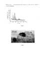
На Фиг. 1 представлена дифрактограмма нитрида кремния, модифицированного фуллереном, после спекания.In FIG. 1 shows a diffraction pattern of fullerene-modified silicon nitride after sintering.
На Фиг. 2 представлено полученное с помощью просвечивающего электронного микроскопа (ПЭМ) JEM-2010 изображение зерен нитрида кремния в спеченном образце.In FIG. Figure 2 shows the image of silicon nitride grains in a sintered sample obtained using a transmission electron microscope (TEM) JEM-2010.
На Фиг. 3 представлены спектры комбинационного рассеяния света (КРС) спеченных образцов керамического материала.In FIG. Figure 3 shows the Raman spectra of sintered samples of ceramic material.
Следующие примеры иллюстрируют предлагаемое изобретение.The following examples illustrate the invention.
Пример 1. Получение керамического наноструктурированного материала на основе нитрида кремния в соответствии с изобретением.Example 1. Obtaining a ceramic nanostructured material based on silicon nitride in accordance with the invention.
В инертной атмосфере смешивают порошок нитрида кремния (фракция меньше 1 мм) с добавлением 3 вес. % фуллерена C60. Полученную смесь засыпают в барабаны и осуществляют обработку в планетарной мельнице со следующими параметрами: время обработки - 30 минут, рабочая частота водила - 550 об/мин. Затем смесь в количестве 2 г загружают в камеру высокого давления типа наковальня с лункой, нагружают до фиксированного давления 4 ГПа и нагревают до температуры 1600°С с временем выдержки 100 с. После разгрузки исследуют структуру и механические свойства образцов. На Фиг. 1 представлена дифрактограмма нитрида кремния, модифицированного фуллереном, после спекания. На Фиг. 2 представлено полученное с помощью просвечивающего электронного микроскопа (ПЭМ) JEM-2010 изображение зерен нитрида кремния в спеченном образце. На Фиг. 3 представлены спектры КРС спеченных образцов керамического материала. Рентгенофазовый анализ и исследование, проведенное с помощью ПЭМ, показывают, что средний размер зерна в керамическом наноструктурированном материале на основе нитрида кремния составляет 20 нм. Эти зерна покрыты ~1 нм углеродным слоем, образовавшимся при спекании из C60. Напрямую получить изображение таких слоев в ПЭМ достаточно сложно, а скоплений углеродного материала размером больше 1 нм, которые могли бы быть обнаружены в образце в случае их наличия, обнаружено не было. Однако идентифицировать слои, которыми покрыты нанокристаллы, можно с помощью спектров КРС. При спекании фуллерен трансформировался в аморфный углерод: на спектрах КРС видны только так называемые D и G пики (фиг. 3) в керамическом наноструктурированном материале на основе нитрида кремния.In an inert atmosphere, silicon nitride powder (fraction less than 1 mm) is mixed with 3 wt. % fullerene C60 . The resulting mixture is poured into drums and processed in a planetary mill with the following parameters: processing time - 30 minutes, operating frequency carrier - 550 rpm Then the mixture in an amount of 2 g is loaded into a high-pressure chamber such as an anvil with a hole, loaded to a fixed pressure of 4 GPa and heated to a temperature of 1600 ° C with a holding time of 100 s. After unloading, the structure and mechanical properties of the samples are examined. In FIG. 1 shows a diffraction pattern of fullerene-modified silicon nitride after sintering. In FIG. Figure 2 shows the image of silicon nitride grains in a sintered sample obtained using a transmission electron microscope (TEM) JEM-2010. In FIG. Figure 3 shows the Raman spectra of sintered samples of ceramic material. An X-ray phase analysis and a TEM study show that the average grain size in a ceramic nanostructured material based on silicon nitride is 20 nm. These grains are covered with ~ 1 nm of a carbon layer formed during sintering from C60 . It is rather difficult to directly image such layers in a TEM, and no accumulations of carbon material larger than 1 nm that could be detected in the sample if they were present were not detected. However, it is possible to identify the layers with which the nanocrystals are coated using Raman spectra. During sintering, fullerene was transformed into amorphous carbon: only so-called D and G peaks are visible on the Raman spectra (Fig. 3) in a ceramic nanostructured material based on silicon nitride.
В результате полученный материал обладает следующими характеристиками: твердость Н=35 ГПа, трещиностойкость К1C=15 МПа√м.As a result, the obtained material has the following characteristics: hardness H = 35 GPa, crack resistance K1C = 15 MPa√m.
Пример 2. Получение керамического наноструктурированного материала на основе нитрида кремния при концентрации фуллерена, отличающейся от оптимальной, приведенной в примере 1.Example 2. Obtaining a ceramic nanostructured material based on silicon nitride at a fullerene concentration that is different from the optimal one given in example 1.
В инертной атмосфере смешивают порошок нитрида кремния (фракция меньше 1 мм) с добавлением 1 вес. % фуллерена C60. Дальнейшие операции проводят аналогично примеру 1. В результате полученный материал обладает следующими характеристиками: твердость Н=28 ГПа, трещиностойкость К1C=13 МПа√м.In an inert atmosphere, silicon nitride powder (fraction less than 1 mm) is mixed with 1 weight added. % fullerene C60 . Further operations are carried out analogously to example 1. As a result, the material obtained has the following characteristics: hardness H = 28 GPa, crack resistance K1C = 13 MPa√m.
Пример 3. Получение керамического наноструктурированного материала на основе нитрида кремния при концентрации фуллерена, отличающейся от оптимальной, приведенной в примере 1.Example 3. Obtaining a ceramic nanostructured material based on silicon nitride at a fullerene concentration that is different from the optimal one given in example 1.
В инертной атмосфере смешивают порошок нитрида кремния (фракция меньше 1 мм) с добавлением 5 вес. % фуллерена C60. Дальнейшие операции проводят аналогично примеру 1. В результате полученный материал обладает следующими характеристиками: твердость Н=25 ГПа, трещиностойкость К1C=14 МПа√м.In an inert atmosphere, silicon nitride powder (fraction less than 1 mm) is mixed with 5 wt. % fullerene C60 . Further operations are carried out analogously to example 1. As a result, the obtained material has the following characteristics: hardness N = 25 GPa, crack resistance K1C = 14 MPa√m.
Пример 4. Получение керамического наноструктурированного материала на основе нитрида кремния в соответствии с изобретением при температурах в температурном диапазоне 1100-1850°С.Example 4. Obtaining a ceramic nanostructured material based on silicon nitride in accordance with the invention at temperatures in the temperature range 1100-1850 ° C.
Изготовляют несколько образцов. Для этого в инертной атмосфере смешивают порошок нитрида кремния (фракция меньше 1 мм) с добавлением 3 вес. % фуллерена С60. Полученную смесь засыпают в барабаны и осуществляют обработку в планетарной мельнице со следующими параметрами: время обработки - 30 минут, рабочая частота водила - 550 об/мин. Затем смесь в количестве 2 г загружают в камеру высокого давления типа наковальня с лункой, нагружают до фиксированного давления 4 ГПа и нагревают до выбранной температуры с временем выдержки 100 с. Были получены образцы при температурах 1100, 1300, 1850°С. В результате полученный материал обладает следующими характеристиками: твердость Н в пределах 25-30 ГПа, трещиностойкость К1C в пределах 13-14 МПа√м.A few samples are made. To do this, in an inert atmosphere, the silicon nitride powder is mixed (fraction less than 1 mm) with the addition of 3 weight. % fullerene C60 . The resulting mixture is poured into drums and processed in a planetary mill with the following parameters: processing time - 30 minutes, operating frequency carrier - 550 rpm Then the mixture in an amount of 2 g is loaded into a high-pressure chamber such as an anvil with a hole, loaded to a fixed pressure of 4 GPa and heated to a selected temperature with a holding time of 100 s. Samples were obtained at temperatures of 1100, 1300, 1850 ° C. As a result, the obtained material has the following characteristics: hardness N in the range of 25-30 GPa, crack resistance K1C in the range of 13-14 MPa√m.
Пример 5. Получение керамического наноструктурированного материала на основе нитрида кремния в соответствии с изобретением в при давлениях 1 и 5 ГПа.Example 5. Obtaining a ceramic nanostructured material based on silicon nitride in accordance with the invention in at pressures of 1 and 5 GPa.
Изготовляют несколько образцов. Для этого в инертной атмосфере смешивают порошок нитрида кремния (фракция меньше 1 мм) с добавлением 3 вес. % фуллерена C60. Полученную смесь засыпают в барабаны и осуществляют обработку в планетарной мельнице со следующими параметрами: время обработки - 30 минут, рабочая частота водила - 550 об/мин. Затем смесь в количестве 2 г загружают в камеру высокого давления типа наковальня с лункой, нагружают до выбранного давления и нагревают до температуры 1600°С с временем выдержки 100 с. Были получены образцы при давлениях 1 и 5 ГПа. В результате полученный материал обладает следующими характеристиками: твердость Н=25 ГПа и трещиностойкость К1C=12 МПа√м для образца, спеченного при давлении 1 ГПа и Н=35 ГПа и трещиностойкость К1C=15 МПа√м для образца, спеченного при давлении 5 ГПа.A few samples are made. To do this, in an inert atmosphere, the silicon nitride powder is mixed (fraction less than 1 mm) with the addition of 3 weight. % fullerene C60 . The resulting mixture is poured into drums and processed in a planetary mill with the following parameters: processing time - 30 minutes, operating frequency carrier - 550 rpm Then the mixture in an amount of 2 g is loaded into a high-pressure chamber such as an anvil with a hole, loaded to a selected pressure and heated to a temperature of 1600 ° C with a holding time of 100 s. Samples were obtained at pressures of 1 and 5 GPa. As a result, the obtained material has the following characteristics: hardness H = 25 GPa and crack resistance K1C = 12 MPa√m for a sample sintered at a pressure of 1 GPa and H = 35 GPa and crack resistance K1C = 15 MPa√m for a sample sintered 5 GPa.

Claims (2)
Translated fromRussianPriority Applications (1)
| Application Number | Priority Date | Filing Date | Title |
|---|---|---|---|
| RU2016142907ARU2653182C2 (en) | 2016-11-01 | 2016-11-01 | Ceramic nanostructured material based on silicon nitride and method of its production |
Applications Claiming Priority (1)
| Application Number | Priority Date | Filing Date | Title |
|---|---|---|---|
| RU2016142907ARU2653182C2 (en) | 2016-11-01 | 2016-11-01 | Ceramic nanostructured material based on silicon nitride and method of its production |
Publications (3)
| Publication Number | Publication Date |
|---|---|
| RU2016142907A RU2016142907A (en) | 2018-05-03 |
| RU2016142907A3 RU2016142907A3 (en) | 2018-05-03 |
| RU2653182C2true RU2653182C2 (en) | 2018-05-07 |
Family
ID=62105645
Family Applications (1)
| Application Number | Title | Priority Date | Filing Date |
|---|---|---|---|
| RU2016142907ARU2653182C2 (en) | 2016-11-01 | 2016-11-01 | Ceramic nanostructured material based on silicon nitride and method of its production |
Country Status (1)
| Country | Link |
|---|---|
| RU (1) | RU2653182C2 (en) |
Citations (5)
| Publication number | Priority date | Publication date | Assignee | Title |
|---|---|---|---|---|
| US4205033A (en)* | 1977-08-22 | 1980-05-27 | Ngk Spark Plug Co., Ltd. | Process for producing compact silicon nitride ceramics |
| SU1073229A1 (en)* | 1981-08-10 | 1984-02-15 | Отделение ордена Ленина института химической физики АН СССР | Method of producing silicon nitride-base material |
| US20040029706A1 (en)* | 2002-02-14 | 2004-02-12 | Barrera Enrique V. | Fabrication of reinforced composite material comprising carbon nanotubes, fullerenes, and vapor-grown carbon fibers for thermal barrier materials, structural ceramics, and multifunctional nanocomposite ceramics |
| US7723248B2 (en)* | 2003-10-29 | 2010-05-25 | Sumitomo Electric Industries, Ltd. | Ceramic composite material and method for producing same |
| WO2014149007A1 (en)* | 2013-03-18 | 2014-09-25 | Ustav Anorganickej Chemie Sav | Composite material with a homogeneous distribution of carbon nanotubes and a method for production of thereof j |
- 2016
- 2016-11-01RURU2016142907Apatent/RU2653182C2/enactive
Patent Citations (5)
| Publication number | Priority date | Publication date | Assignee | Title |
|---|---|---|---|---|
| US4205033A (en)* | 1977-08-22 | 1980-05-27 | Ngk Spark Plug Co., Ltd. | Process for producing compact silicon nitride ceramics |
| SU1073229A1 (en)* | 1981-08-10 | 1984-02-15 | Отделение ордена Ленина института химической физики АН СССР | Method of producing silicon nitride-base material |
| US20040029706A1 (en)* | 2002-02-14 | 2004-02-12 | Barrera Enrique V. | Fabrication of reinforced composite material comprising carbon nanotubes, fullerenes, and vapor-grown carbon fibers for thermal barrier materials, structural ceramics, and multifunctional nanocomposite ceramics |
| US7723248B2 (en)* | 2003-10-29 | 2010-05-25 | Sumitomo Electric Industries, Ltd. | Ceramic composite material and method for producing same |
| WO2014149007A1 (en)* | 2013-03-18 | 2014-09-25 | Ustav Anorganickej Chemie Sav | Composite material with a homogeneous distribution of carbon nanotubes and a method for production of thereof j |
Also Published As
| Publication number | Publication date |
|---|---|
| RU2016142907A (en) | 2018-05-03 |
| RU2016142907A3 (en) | 2018-05-03 |
Similar Documents
| Publication | Publication Date | Title |
|---|---|---|
| US9422161B2 (en) | Ultrahard nanotwinned boron nitride bulk materials and synthetic method thereof | |
| Inam et al. | Structural and chemical stability of multiwall carbon nanotubes in sintered ceramic nanocomposite | |
| Zhang et al. | Related mechanism of transparency in MgAl2O4 nano-ceramics prepared by sintering under high pressure and low temperature | |
| Bonache et al. | Synthesis and processing of nanocrystalline tungsten carbide: Towards cemented carbides with optimal mechanical properties | |
| Wu et al. | High-pressure synthesis of tungsten carbide–cubic boron nitride (WC–cBN) composites: Effect of cBN particle size and volume fraction on their microstructure and properties | |
| Wu et al. | High pressure synthesis of tungsten carbide–cubic boron nitride (WC–cBN) composites: Effect of thermodynamic condition and cBN volume fraction on their microstructure and properties | |
| Huang et al. | Rapid densification and mechanical properties of ultra-high-pressure sintered transition metal carbide ceramics | |
| Dedova et al. | The study on thermal expansion of ceramic composites with addition of ZrW2O8 | |
| Wang et al. | Study on the properties and fracture mode of pure polycrystalline cubic boron nitride with different particle sizes | |
| CN106829968A (en) | A kind of method that use phase transition under high pressure method prepares nano-multicrystal stishovite | |
| RU2653182C2 (en) | Ceramic nanostructured material based on silicon nitride and method of its production | |
| Zharikov et al. | Preparation of SiC–MgAl2O4–Y3Al5O12-MWCNTs nanocomposites by spark plasma sintering | |
| Ovsyannikov et al. | High-hardness ceramics based on boron carbide fullerite derivatives | |
| Dakova et al. | Effect of sintering time on mechanical properties of (Hf-Ta-Zr-Nb-Ti) C | |
| Kul’met’yeva et al. | ZrO2–Y2O3 ceramic composite modified by multilayered graphene | |
| RU2627522C2 (en) | Ceramic corundum-based material and method of its production | |
| Senyut et al. | Synthesis of polycrystalline cubic boron nitride from hexagonal boron nitride after mechanical activation and modification with aluminum | |
| US20160137510A1 (en) | Ultrahard nanotwinned diamond bulk material and method for preparing the same | |
| Jia et al. | Effects of initial crystal size of diamond powder on surface residual stress and morphology in polycrystalline diamond (PCD) layer | |
| Mashhadi et al. | Fabrication of bulk AlN–TiN nanocomposite by reactive ball milling and underwater shock consolidation technique | |
| Kolmakov et al. | Structure, properties, and applications of ceramic composite produced of nanostructured powders of composition ZrO2+ 3% Y2O3 | |
| Pithan et al. | Consolidation, microstructure and crystallography of dense NaNbO3 ceramics with ultra-fine grain size | |
| Li et al. | Rediscovering the intrinsic mechanical properties of bulk nanocrystalline indium arsenide | |
| Oglezneva et al. | Structure and characteristics of functional powder composite materials obtained by spark plasma sintering | |
| Kul’met’eva et al. | Preparation of zirconia ceramics from powder synthesized by a sol-gel method |
Legal Events
| Date | Code | Title | Description |
|---|---|---|---|
| QB4A | Licence on use of patent | Free format text:LICENCE FORMERLY AGREED ON 20200110 Effective date:20200110 |