RU2636055C2 - Led lattice device and method of manufacturing led lattice device - Google Patents
Led lattice device and method of manufacturing led lattice deviceDownload PDFInfo
- Publication number
- RU2636055C2 RU2636055C2RU2014146311ARU2014146311ARU2636055C2RU 2636055 C2RU2636055 C2RU 2636055C2RU 2014146311 ARU2014146311 ARU 2014146311ARU 2014146311 ARU2014146311 ARU 2014146311ARU 2636055 C2RU2636055 C2RU 2636055C2
- Authority
- RU
- Russia
- Prior art keywords
- led
- heat
- plate
- shaped part
- conducting element
- Prior art date
Links
- 238000004519manufacturing processMethods0.000titleclaimsdescription9
- 238000000034methodMethods0.000claimsdescription19
- 230000000712assemblyEffects0.000claimsdescription15
- 238000000429assemblyMethods0.000claimsdescription15
- 238000009966trimmingMethods0.000claimsdescription4
- 238000005452bendingMethods0.000claims3
- 230000015572biosynthetic processEffects0.000claims2
- 239000000126substanceSubstances0.000abstract1
- 238000003491arrayMethods0.000description3
- 239000011230binding agentSubstances0.000description3
- 239000000463materialSubstances0.000description3
- 238000009434installationMethods0.000description2
- 230000003287optical effectEffects0.000description2
- 238000005476solderingMethods0.000description2
- 238000001816coolingMethods0.000description1
- 239000003292glueSubstances0.000description1
- 230000017525heat dissipationEffects0.000description1
- 239000011810insulating materialSubstances0.000description1
- 238000012986modificationMethods0.000description1
- 230000004048modificationEffects0.000description1
- 229910000679solderInorganic materials0.000description1
Images


Classifications
- H—ELECTRICITY
- H05—ELECTRIC TECHNIQUES NOT OTHERWISE PROVIDED FOR
- H05K—PRINTED CIRCUITS; CASINGS OR CONSTRUCTIONAL DETAILS OF ELECTRIC APPARATUS; MANUFACTURE OF ASSEMBLAGES OF ELECTRICAL COMPONENTS
- H05K7/00—Constructional details common to different types of electric apparatus
- H05K7/20—Modifications to facilitate cooling, ventilating, or heating
- F—MECHANICAL ENGINEERING; LIGHTING; HEATING; WEAPONS; BLASTING
- F21—LIGHTING
- F21V—FUNCTIONAL FEATURES OR DETAILS OF LIGHTING DEVICES OR SYSTEMS THEREOF; STRUCTURAL COMBINATIONS OF LIGHTING DEVICES WITH OTHER ARTICLES, NOT OTHERWISE PROVIDED FOR
- F21V23/00—Arrangement of electric circuit elements in or on lighting devices
- F21V23/001—Arrangement of electric circuit elements in or on lighting devices the elements being electrical wires or cables
- F—MECHANICAL ENGINEERING; LIGHTING; HEATING; WEAPONS; BLASTING
- F21—LIGHTING
- F21K—NON-ELECTRIC LIGHT SOURCES USING LUMINESCENCE; LIGHT SOURCES USING ELECTROCHEMILUMINESCENCE; LIGHT SOURCES USING CHARGES OF COMBUSTIBLE MATERIAL; LIGHT SOURCES USING SEMICONDUCTOR DEVICES AS LIGHT-GENERATING ELEMENTS; LIGHT SOURCES NOT OTHERWISE PROVIDED FOR
- F21K9/00—Light sources using semiconductor devices as light-generating elements, e.g. using light-emitting diodes [LED] or lasers
- F21K9/20—Light sources comprising attachment means
- F—MECHANICAL ENGINEERING; LIGHTING; HEATING; WEAPONS; BLASTING
- F21—LIGHTING
- F21K—NON-ELECTRIC LIGHT SOURCES USING LUMINESCENCE; LIGHT SOURCES USING ELECTROCHEMILUMINESCENCE; LIGHT SOURCES USING CHARGES OF COMBUSTIBLE MATERIAL; LIGHT SOURCES USING SEMICONDUCTOR DEVICES AS LIGHT-GENERATING ELEMENTS; LIGHT SOURCES NOT OTHERWISE PROVIDED FOR
- F21K9/00—Light sources using semiconductor devices as light-generating elements, e.g. using light-emitting diodes [LED] or lasers
- F21K9/90—Methods of manufacture
- F—MECHANICAL ENGINEERING; LIGHTING; HEATING; WEAPONS; BLASTING
- F21—LIGHTING
- F21K—NON-ELECTRIC LIGHT SOURCES USING LUMINESCENCE; LIGHT SOURCES USING ELECTROCHEMILUMINESCENCE; LIGHT SOURCES USING CHARGES OF COMBUSTIBLE MATERIAL; LIGHT SOURCES USING SEMICONDUCTOR DEVICES AS LIGHT-GENERATING ELEMENTS; LIGHT SOURCES NOT OTHERWISE PROVIDED FOR
- F21K99/00—Subject matter not provided for in other groups of this subclass
- F—MECHANICAL ENGINEERING; LIGHTING; HEATING; WEAPONS; BLASTING
- F21—LIGHTING
- F21S—NON-PORTABLE LIGHTING DEVICES; SYSTEMS THEREOF; VEHICLE LIGHTING DEVICES SPECIALLY ADAPTED FOR VEHICLE EXTERIORS
- F21S4/00—Lighting devices or systems using a string or strip of light sources
- F21S4/10—Lighting devices or systems using a string or strip of light sources with light sources attached to loose electric cables, e.g. Christmas tree lights
- F21S4/15—Lighting devices or systems using a string or strip of light sources with light sources attached to loose electric cables, e.g. Christmas tree lights the cables forming a grid, net or web structure
- F—MECHANICAL ENGINEERING; LIGHTING; HEATING; WEAPONS; BLASTING
- F21—LIGHTING
- F21V—FUNCTIONAL FEATURES OR DETAILS OF LIGHTING DEVICES OR SYSTEMS THEREOF; STRUCTURAL COMBINATIONS OF LIGHTING DEVICES WITH OTHER ARTICLES, NOT OTHERWISE PROVIDED FOR
- F21V23/00—Arrangement of electric circuit elements in or on lighting devices
- F—MECHANICAL ENGINEERING; LIGHTING; HEATING; WEAPONS; BLASTING
- F21—LIGHTING
- F21V—FUNCTIONAL FEATURES OR DETAILS OF LIGHTING DEVICES OR SYSTEMS THEREOF; STRUCTURAL COMBINATIONS OF LIGHTING DEVICES WITH OTHER ARTICLES, NOT OTHERWISE PROVIDED FOR
- F21V29/00—Protecting lighting devices from thermal damage; Cooling or heating arrangements specially adapted for lighting devices or systems
- F21V29/50—Cooling arrangements
- F21V29/70—Cooling arrangements characterised by passive heat-dissipating elements, e.g. heat-sinks
- H—ELECTRICITY
- H05—ELECTRIC TECHNIQUES NOT OTHERWISE PROVIDED FOR
- H05K—PRINTED CIRCUITS; CASINGS OR CONSTRUCTIONAL DETAILS OF ELECTRIC APPARATUS; MANUFACTURE OF ASSEMBLAGES OF ELECTRICAL COMPONENTS
- H05K7/00—Constructional details common to different types of electric apparatus
- H05K7/20—Modifications to facilitate cooling, ventilating, or heating
- H05K7/2039—Modifications to facilitate cooling, ventilating, or heating characterised by the heat transfer by conduction from the heat generating element to a dissipating body
- H05K7/20509—Multiple-component heat spreaders; Multi-component heat-conducting support plates; Multi-component non-closed heat-conducting structures
- F—MECHANICAL ENGINEERING; LIGHTING; HEATING; WEAPONS; BLASTING
- F21—LIGHTING
- F21Y—INDEXING SCHEME ASSOCIATED WITH SUBCLASSES F21K, F21L, F21S and F21V, RELATING TO THE FORM OR THE KIND OF THE LIGHT SOURCES OR OF THE COLOUR OF THE LIGHT EMITTED
- F21Y2105/00—Planar light sources
- F21Y2105/10—Planar light sources comprising a two-dimensional array of point-like light-generating elements
- F—MECHANICAL ENGINEERING; LIGHTING; HEATING; WEAPONS; BLASTING
- F21—LIGHTING
- F21Y—INDEXING SCHEME ASSOCIATED WITH SUBCLASSES F21K, F21L, F21S and F21V, RELATING TO THE FORM OR THE KIND OF THE LIGHT SOURCES OR OF THE COLOUR OF THE LIGHT EMITTED
- F21Y2115/00—Light-generating elements of semiconductor light sources
- F21Y2115/10—Light-emitting diodes [LED]
- H—ELECTRICITY
- H01—ELECTRIC ELEMENTS
- H01L—SEMICONDUCTOR DEVICES NOT COVERED BY CLASS H10
- H01L2924/00—Indexing scheme for arrangements or methods for connecting or disconnecting semiconductor or solid-state bodies as covered by H01L24/00
- H01L2924/0001—Technical content checked by a classifier
- H01L2924/0002—Not covered by any one of groups H01L24/00, H01L24/00 and H01L2224/00
- H—ELECTRICITY
- H10—SEMICONDUCTOR DEVICES; ELECTRIC SOLID-STATE DEVICES NOT OTHERWISE PROVIDED FOR
- H10H—INORGANIC LIGHT-EMITTING SEMICONDUCTOR DEVICES HAVING POTENTIAL BARRIERS
- H10H20/00—Individual inorganic light-emitting semiconductor devices having potential barriers, e.g. light-emitting diodes [LED]
- H10H20/80—Constructional details
- H10H20/85—Packages
- H10H20/8506—Containers
- H—ELECTRICITY
- H10—SEMICONDUCTOR DEVICES; ELECTRIC SOLID-STATE DEVICES NOT OTHERWISE PROVIDED FOR
- H10H—INORGANIC LIGHT-EMITTING SEMICONDUCTOR DEVICES HAVING POTENTIAL BARRIERS
- H10H20/00—Individual inorganic light-emitting semiconductor devices having potential barriers, e.g. light-emitting diodes [LED]
- H10H20/80—Constructional details
- H10H20/85—Packages
- H10H20/857—Interconnections, e.g. lead-frames, bond wires or solder balls
Landscapes
- Engineering & Computer Science (AREA)
- General Engineering & Computer Science (AREA)
- Physics & Mathematics (AREA)
- Microelectronics & Electronic Packaging (AREA)
- Optics & Photonics (AREA)
- Thermal Sciences (AREA)
- Manufacturing & Machinery (AREA)
- Led Device Packages (AREA)
- Devices For Indicating Variable Information By Combining Individual Elements (AREA)
- Arrangement Of Elements, Cooling, Sealing, Or The Like Of Lighting Devices (AREA)
Abstract
Description
Translated fromRussianОБЛАСТЬ ТЕХНИКИFIELD OF TECHNOLOGY
Данное изобретение относится к светодиодному решетчатому (сетчатому) устройству и способу изготовления светодиодного решетчатого устройства.This invention relates to an LED grating (mesh) device and a method for manufacturing an LED grating.
УРОВЕНЬ ТЕХНИКИBACKGROUND
В общем, светодиодные решетки (сетки) изготавливаются посредством соединения нескольких рядов светодиодных модулей при помощи набора из нескольких параллельных проводов, где этот набор проводов имеет начальную ширину, а затем растяжения этого набора проводов до большей ширины, с образованием, таким образом, решетки. Один пример такой светодиодной решетки предшествующего уровня техники раскрывается в патенте США 7942551.In general, LED gratings (grids) are made by connecting several rows of LED modules using a set of several parallel wires, where this set of wires has an initial width, and then stretching this set of wires to a larger width, thus forming a grating. One example of such a prior art LED array is disclosed in US Pat. No. 7,942,551.
Светодиодная решетка обычно размещается на пластине (плате) из некоторого материала или очень близко к ней или размещается в промежутке между двумя пластинами, причем по меньшей мере одна из них является пропускающей свет, и, таким образом, образуется светодиодное решетчатое устройство. Основной проблемой в отношении светодиодов является отвод тепла. Эффективность светодиодов зависит от их температуры. В светодиодных решетках большая часть тепла отводится через провода. Это ограничивает мощность, которая может быть подана на светодиоды, в частности, когда светодиодная решетка расположена на пластине или между двумя пластинами.An LED array is usually placed on a plate (circuit board) of some material or very close to it or is placed in the gap between two plates, at least one of which is light transmitting, and thus an LED array is formed. The main problem with LEDs is heat dissipation. The effectiveness of LEDs depends on their temperature. In LED arrays, most of the heat is removed through the wires. This limits the power that can be supplied to the LEDs, in particular when the LED array is located on a plate or between two plates.
СУЩНОСТЬ ИЗОБРЕТЕНИЯSUMMARY OF THE INVENTION
Задачей данного изобретения является обеспечение светодиодного решетчатого устройства и способа для изготовления светодиодного решетчатого устройства, который смягчает вышеупомянутые проблемы предшествующего уровня техники, и позволяет осуществить подведение к этим светодиодам более высокой мощности, чем мощность, подводимая к светодиодным решеткам предшествующего уровня техники.An object of the present invention is to provide an LED grating device and a method for manufacturing an LED grating device that mitigates the aforementioned problems of the prior art and allows bringing higher power to these LEDs than the power supplied to the LED grating of the prior art.
Данное изобретение основано на понимании, что добавление охлаждающего элемента в светодиодную сборку является возможным и эффективным.This invention is based on the understanding that the addition of a cooling element to the LED assembly is possible and effective.
В первом аспекте данного изобретения, эта задача достигается посредством светодиодного решетчатого устройства, содержащего светодиодную решетку, размещенную на детали пластинчатой формы, где эта светодиодная решетка содержит множество электрически проводящих проводов, размещенных рядом (бок о бок), и множество светодиодных модулей, причем каждый светодиодный модуль содержит светодиодную сборку, присоединенную по меньшей мере к двум проводам из числа электрически проводящих проводов, и теплопроводящий элемент, расположенный между двумя соседними проводами из числа проводов, к которым присоединена светодиодная сборка, где этот теплопроводящий элемент несет светодиодную сборку и выступает из-под светодиодной сборки, и где этот теплопроводящий элемент прикрепляется к детали пластинчатой формы. Таким образом, обеспечивается дополнительный элемент, который функционирует в качестве радиатора.In a first aspect of the present invention, this task is achieved by means of an LED grating device comprising an LED grating arranged on a plate-like part, where this LED grating comprises a plurality of electrically conductive wires arranged side by side (side by side) and a plurality of LED modules, each LED the module contains an LED assembly connected to at least two wires from among the electrically conductive wires, and a heat-conducting element located between the two knowing the neighboring wires from the number of wires to which the LED assembly is connected, where this heat-conducting element carries the LED assembly and protrudes from under the LED assembly, and where this heat-conducting element is attached to the plate-shaped part. This provides an additional element that functions as a radiator.
В соответствии с одним (некоторым) вариантом осуществления светодиодного решетчатого устройства, каждый теплопроводящий элемент содержит промежуточный участок, который несет светодиодную сборку, и первый и второй выступы, которые выступают из этого промежуточного участка в противоположных направлениях. Этот вариант осуществления предусматривает усиленное закрепление светодиодных модулей.In accordance with one (some) embodiment of the LED array device, each heat-conducting element comprises an intermediate portion that carries the LED assembly and first and second protrusions that protrude from this intermediate portion in opposite directions. This embodiment provides reinforced fixing of the LED modules.
В соответствии с одним (некоторым) вариантом осуществления светодиодного решетчатого устройства, каждый теплопроводящий элемент имеет форму ленты и является плоским, по меньшей мере на той стороне, к которой прикреплена светодиодная сборка. Одна сторона теплопроводящего элемента прикрепляется к светодиодной сборке, а противоположная сторона теплопроводящего элемента обращена к детали пластинчатой формы.In accordance with one (some) embodiment of the LED grating device, each heat-conducting element is in the form of a tape and is flat, at least on the side to which the LED assembly is attached. One side of the heat-conducting element is attached to the LED assembly, and the opposite side of the heat-conducting element is facing the plate-shaped part.
В соответствии с одним (некоторым) вариантом осуществления светодиодного решетчатого устройства, по меньшей мере первый участок каждого первого и второго выступов каждого теплопроводящего элемента продолжается под углом к промежуточному участку. Таким образом, получаются гибкие условия монтажа.According to one (some) embodiment of the LED grating, at least a first portion of each of the first and second protrusions of each heat-conducting element extends at an angle to the intermediate portion. Thus, flexible installation conditions are obtained.
В соответствии с одним (некоторым) вариантом осуществления светодиодного решетчатого устройства, указанный по меньшей мере первый участок каждого первого и второго выступов продолжается в деталь пластинчатой формы. Другими словами, по меньшей мере часть каждого выступа вставлена в деталь пластинчатой формы. Это является предпочтительным способом монтажа светодиодной решетки на деталь пластинчатой формы.In accordance with one (some) embodiment of an LED grating device, said at least a first portion of each first and second protrusions extends into a plate-shaped part. In other words, at least a portion of each protrusion is inserted into the plate-shaped part. This is the preferred method of mounting the LED array on a plate-shaped part.
В соответствии с одним (некоторым) вариантом осуществления светодиодного решетчатого устройства, второй участок каждого первого и второго выступов каждого теплопроводящего элемента выступает из детали пластинчатой формы на противоположной стороне детали пластинчатой формы относительно стороны, на которой размещается промежуточный участок. Этот вариант осуществления является полезным для отвода тепла за пределы детали пластинчатой формы, в частности, если деталь пластинчатой формы выполнена из изолирующего материала.In accordance with one (some) embodiment of the LED grating, a second portion of each first and second protrusions of each heat-conducting element protrudes from the plate-shaped part on the opposite side of the plate-shaped part relative to the side on which the intermediate portion is placed. This embodiment is useful for dissipating heat outside a plate-shaped part, in particular if the plate-shaped part is made of insulating material.
В соответствии с одним (некоторым) вариантом осуществления светодиодного решетчатого устройства, по меньшей мере первый участок каждого первого и второго выступов каждого теплопроводящего элемента продолжается за светодиодную сборку. Конечный участок каждого первого и второго выступов каждого теплопроводящего элемента продолжается параллельно промежуточному участку и прикрепляется к поверхности детали пластинчатой формы, где светоизлучающая поверхность светодиодной сборки обращена к указанной поверхности детали пластинчатой формы. Этот вариант осуществления обеспечивает простой способ управления расстоянием от светодиода до детали пластинчатой формы, которая в этом случае обычно является пропускающей свет.According to one (some) embodiment of the LED grating, at least a first portion of each of the first and second protrusions of each heat-conducting element extends beyond the LED assembly. The end portion of each of the first and second protrusions of each heat-conducting element extends parallel to the intermediate portion and is attached to the surface of the plate-shaped part, where the light-emitting surface of the LED assembly faces the specified surface of the plate-shaped part. This embodiment provides an easy way to control the distance from the LED to the plate-shaped part, which in this case is usually light transmitting.
Во втором аспекте данного изобретения, задача достигается посредством способа изготовления светодиодного решетчатого устройства, содержащего стадии размещения рядом нескольких электрически проводящих проводов, с образованием, таким образом, набора проводов, имеющего начальную ширину; присоединения нескольких светодиодных сборок к этому набору проводов таким образом, чтобы каждая светодиодная сборка присоединялась по меньшей мере к двум проводам этого набора проводов, и, таким образом, чтобы образовались несколько параллельных рядов светодиодных сборок; прикрепления соответствующей теплопроводящей ленты к светодиодным сборкам каждого ряда; подрезки каждой ленты для образования отдельных теплопроводящих элементов для каждой светодиодной сборки; растяжения набора проводов до второй ширины, которая является большей, чем первая (начальная) ширина; и монтажа набора проводов на детали пластинчатой формы, и прикрепления каждого теплопроводящего элемента к детали пластинчатой формы.In a second aspect of the invention, the object is achieved by a method for manufacturing an LED grating device comprising the steps of placing several electrically conductive wires side by side, thereby forming a set of wires having an initial width; attaching several LED assemblies to this set of wires so that each LED assembly is connected to at least two wires of this set of wires, and so that several parallel rows of LED assemblies are formed; attaching the corresponding heat-conducting tape to the LED assemblies of each row; trimming each strip to form separate heat-conducting elements for each LED assembly; stretching a set of wires to a second width that is larger than the first (initial) width; and mounting a set of wires on the plate-shaped part, and attaching each heat-conducting element to the plate-shaped part.
Задача данного изобретения, изложенная выше, также решается посредством этого способа. Варианты осуществления этого способа обеспечивают преимущества, соответствующие преимуществам, изложенным выше, в связи с вариантами осуществления светодиодного решетчатого устройства.The objective of the invention described above is also solved by this method. Embodiments of this method provide benefits consistent with the advantages set forth above in connection with embodiments of an LED grating device.
Эти и другие аспекты и преимущества данного изобретения явствуют из вариантов осуществления, описанных ниже, и будут объяснены со ссылкой на них.These and other aspects and advantages of the present invention will be apparent from the embodiments described below and will be explained with reference to them.
КРАТКОЕ ОПИСАНИЕ ЧЕРТЕЖЕЙBRIEF DESCRIPTION OF THE DRAWINGS
Данное изобретение будет теперь описано более подробно и со ссылкой на приложенные чертежи, в которых:The present invention will now be described in more detail and with reference to the attached drawings, in which:
Фигуры 1а и 1b схематично показывают первый вариант осуществления светодиодного решетчатого устройства согласно данному изобретению;Figures 1a and 1b schematically show a first embodiment of an LED grating device according to this invention;
Фигуры 2а-2с схематично показывают второй вариант осуществления светодиодного решетчатого устройства;Figures 2a-2c schematically show a second embodiment of an LED grating device;
Фигуры 3а-3с схематично показывают часть третьего варианта осуществления светодиодного решетчатого устройства;Figures 3a-3c schematically show part of a third embodiment of an LED grating device;
Фигура 4 схематично иллюстрирует один (некоторый) вариант осуществления способа изготовления светодиодного решетчатого устройства согласно данному изобретению.Figure 4 schematically illustrates one (some) embodiment of a method for manufacturing an LED grating device according to this invention.
ПОДРОБНОЕ ОПИСАНИЕ ВАРИАНТОВ ОСУЩЕСТВЛЕНИЯDETAILED DESCRIPTION OF EMBODIMENTS
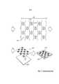
Со ссылкой на фигуры 1а и 1b, первый вариант осуществления светодиодного решетчатого устройства 100 данного изобретения содержит светодиодную решетку 102, и деталь 104 пластинчатой формы, к которой прикреплена светодиодная решетка 102. В этом варианте осуществления деталь 104 пластинчатой формы является нижней (опорной) пластиной светодиодного решетчатого устройства 100. На фигуре 1а светодиодное решетчатое устройство 100 показано снизу, т.е. со стороны детали 104 пластинчатой формы, которая просто указана пунктирным прямоугольником. Фигура 1b является перспективным видом наклонно сверху. Светодиодная решетка 102 содержит несколько электрически проводящих проводов 106, размещенных рядом, и несколько светодиодных модулей 108. Каждый светодиодный модуль содержит светодиодную сборку 110, где каждая светодиодная сборка 110 присоединяется по меньшей мере к двум проводам 106 из числа электрически проводящих проводов 106. Каждый светодиодный модуль дополнительно содержит теплопроводящий элемент 112, расположенный между двумя соседними проводами 106 из числа проводов, к которым прикрепляется светодиодная сборка 110. Теплопроводящий элемент 112 несет светодиодную сборку и прикрепляется к детали 104 пластинчатой формы. Теплопроводящий элемент 112 выступает из-под светодиодной сборки 110. Более конкретно, в этом варианте осуществления теплопроводящий элемент 112 имеет форму ленты и является плоским, и он имеет промежуточный участок 114, который несет светодиодную сборку 110, и первый и второй выступы 116, 118, которые выступают из промежуточного участка 114 в противоположных направлениях. Сама светоизлучающая поверхность 120 обеспечивается на верхней стороне светодиодной сборки 110, в то время как теплопроводящий элемент 112 присоединяется к нижней стороне светодиодной сборки 110. Если требуется, дополнительная деталь пластинчатой формы, обычно имеющая оптические характеристики, размещается наверху светодиодного модуля 108, и является параллельной детали 104 пластинчатой формы, образующей нижнюю часть (основание) светодиодного решетчатого устройства 100, и противоположной ей.With reference to figures 1a and 1b, the first embodiment of the
Теплопроводящий элементы 112 являются электрически изолированными, и они присоединены к детали 104 пластинчатой формы посредством соответствующего способа присоединения, который может зависеть от материала детали 104 пластинчатой формы. Например, теплопроводящий элемент 112 прикрепляется к детали 104 пластинчатой формы посредством, например, связующего вещества, а к светодиодным сборкам 110, посредством соединения пайкой, термического клея или любого термически эффективного межкомпонентного соединения. Теплопроводящий элемент 112 по существу увеличивает площадь поверхности светодиодного модуля 108 и по существу увеличивает рассеяние тепла в окружающую среду. Предпочтительно, деталь 104 пластинчатой формы также является теплопроводящей, но это не является необходимым.The heat-conducting
Фигуры 2а-2 с показывают второй вариант осуществления, который является аналогичным первому варианту осуществления в большинстве отношений. Таким образом, второй вариант осуществления светодиодного решетчатого устройства 200 содержит светодиодную решетку 202, деталь 204 пластинчатой формы, образующей нижнюю пластину, к которой присоединена светодиодная решетка 202. Светодиодная решетка 202 содержит несколько электрически проводящих проводов 206, размещенных рядом, и несколько светодиодных модулей 208, причем каждый из них содержит светодиодную сборку 210, присоединенную к проводам 206, и теплопроводящий элемент 212, расположенный между двумя соседними проводами 206. Теплопроводящий элемент 212 несет светодиодную сборку 210, и прикрепляется к детали 204 пластинчатой формы. Теплопроводящий элемент 112 имеет промежуточный участок 214, и первый и второй выступы 216, 218.Figures 2a-2c show a second embodiment that is similar to the first embodiment in most respects. Thus, the second embodiment of the
Однако форма и прикрепление теплопроводящего элемента 212 отличается от первого варианта осуществления. Считается, что каждый выступ может иметь первый участок 220, 222, который продолжается от промежуточного участка 214, и второй участок 224, 226, который является конечным участком и продолжается от первого участка 220, 222. Теплопроводящий элемент 212 согнут таким образом, чтобы первый участок 220, 222 каждого первого и второго выступов 216, 218 продолжается под углом к промежуточному участку 214. Более конкретно, этот угол составляет около 90 градусов. Второй участок 224, 226 продолжается, приближенно, параллельно промежуточному участку 214. Первый участок 220, 222 каждого первого и второго выступов 216, 218 продолжается в деталь 204 пластинчатой формы, а вторые участки 224, 226 выступают из детали 204 пластинчатой формы на противоположной стороне детали 204 пластинчатой формы относительно стороны, на которой размещается промежуточный участок 214, т.е. на задней стороне или нижней стороне детали 204 пластинчатой формы. Альтернативно, вторые участки 224, 226 не являются согнутыми относительно первых участков 220, 222, но продолжаются параллельно первым участкам 220, 222. Это означает, что теплопроводящий элемент 212 имеет форму скобки.However, the shape and attachment of the heat-conducting
Второй вариант осуществления светодиодного решетчатого устройства 200 является, в частности, полезным, когда деталь 204 пластинчатой формы является термически изолирующей, где генерируемое тепло транспортируется вдоль теплопроводящего элемента 212 через деталь 204 пластинчатой формы и выделяется в окружающую среду на ее задней стороне.A second embodiment of the
Согнутые конечные участки 224, 226 гарантируют, что светодиодные модули 208 хорошо закреплены на детали 204 пластинчатой формы, и делают ненужным использование связующего вещества. Однако, в зависимости от материала детали 204 пластинчатой формы, светодиодные модули 208 могут также хорошо прикрепляться при помощи теплопроводящего элемента в форме скобки.The
Со ссылкой на фигуры 3а-3с, третий вариант осуществления светодиодного решетчатого устройства 300, который разделяет многие признаки с первым и вторым вариантами осуществления, содержит светодиодную решетку 302, и деталь 304 пластинчатой формы, к которой светодиодная решетка 302 прикреплена. Однако в этом варианте осуществления деталь 304 пластинчатой формы является верхней пластиной, как будет дополнительно описано ниже. Светодиодная решетка 302 содержит несколько электрически проводящих проводов 306, размещенных рядом, и несколько светодиодных модулей 308, причем каждый из них содержит светодиодную сборку 310, присоединенную к проводам 306, и теплопроводящий элемент 312, расположенный между двумя соседними проводами 306. Однако, исходя из соображений простоты, показан только один светодиодный модуль 308. Теплопроводящий элемент 312 несет светодиодную сборку 310, и прикрепляется к детали 304 пластинчатой формы. Теплопроводящий элемент 312 имеет промежуточный участок 314, и первый и второй выступы 316, 318.With reference to figures 3a-3c, a third embodiment of an
Аналогично второму варианту осуществления, каждый выступ имеет первый участок 320, 322, продолжающийся под углом к промежуточному участку 314, и второй участок, который является конечным участком, 324, 326, продолжающимся параллельно промежуточному участку. Однако, предпочтительно, этот угол составляет менее 90 градусов, и каждый первый участок 320, 322 продолжается за светодиодную сборку 310. Конечный участок 324, 326 каждого первого и второго выступов 316, 318 продолжается параллельно промежуточному участку 314 и прикрепляется к нижней поверхности детали 304 пластинчатой формы, где светоизлучающая поверхность 328 светодиодной сборки 310 обращена к нижней поверхности детали 304 пластинчатой формы. Другими словами, теплопроводящий элемент 312 работает подобно чаше, где светодиодный модуль 308 расположен на дне этой чаши, а деталь 304 пластинчатой формы является крышкой этой чаши. В этом третьем варианте осуществления деталь 304 пластинчатой формы является пропускающей свет и оптической, как например, просто прозрачной или, более часто, рассеивающей. Однако, альтернативно, деталь 304 пластинчатой формы может быть отражающей таким образом, чтобы свет выходил в противоположном направлении.Similarly to the second embodiment, each protrusion has a
Теплопроводящий элемент 312 может снабжаться светоотражающей верхней поверхностью, таким образом, отражая свет в направлении детали 304 пластинчатой формы.The heat-conducting
Со ссылкой на фигуру 4, один (некоторый) вариант осуществления способа изготовления светодиодного решетчатого устройства показан посредством ряда изображений, показывающих последовательные стадии процесса изготовления. Этот способ содержит размещение рядом нескольких электрически проводящих проводов 406, с образованием, таким образом, набора 407 проводов, имеющих начальную ширину D1; присоединение нескольких светодиодных сборок 410 к этому набору 407 проводов таким образом, чтобы каждая светодиодная сборка 410 присоединялась по меньшей мере к двум проводам этого набора проводов, и, таким образом, чтобы образовались несколько параллельных рядов светодиодных сборок 410; и снабжение каждой светодиодной сборки теплопроводящим элементом 412, с получением, таким образом, светодиодной решетки 402. Следует отметить, что эти стадии могут выполняться в том порядке, в котором они представлены здесь, или в другом порядке, в зависимости от того, как выполняется сборка (монтаж). Например, светодиодные сборки могут располагаться в зажимном приспособлении, и обеспечиваются провода 406 и теплопроводящие элементы 412.With reference to FIG. 4, one (some) embodiment of a method for manufacturing an LED array device is shown by a series of images showing successive stages of a manufacturing process. This method comprises placing several electrically
Этот способ дополнительно содержит растяжение светодиодной решетки 402 до второй ширины D2, где D2 является большей, чем D1; и монтаж светодиодной решетки 402 на деталь 404 пластинчатой формы, что включает в себя прикрепление каждого теплопроводящего элемента 412 к детали 404 пластинчатой формы. Таким образом, светодиодное решетчатое устройство 400 изготовлено.This method further comprises stretching the
Операция обеспечения каждой светодиодной сборки 410 теплопроводящим элементом 412 содержит прикрепление соответствующей теплопроводящей ленты 409 к светодиодным сборкам 410 каждого ряда; и подрезку каждой ленты 409 для образования отдельных теплопроводящих элементов 412 для каждой светодиодной сборки 410. Альтернативно, но менее предпочтительно, теплопроводящие элементы 412 подрезаются заранее и прикрепляются отдельно к светодиодным сборкам 410. Кроме того, в качестве альтернативы, сначала провода 406 размещаются рядом, затем теплопроводящие ленты 409 располагаются между проводами 406, и затем светодиодные сборки 410 монтируются на эти провода и на эти теплопроводящие ленты 409. В качестве дополнительной альтернативы, светодиодные сборки располагаются в зажимном приспособлении, в перевернутом положении, и затем теплопроводящие ленты 409 монтируются на эти светодиодные сборки, и, наконец, провода 406 монтируются на эти светодиодные сборки. Эти различные альтернативы предусматривают различные преимущества.The operation of providing each
Что касается расположения светодиодных сборок 410, они размещаются таким образом, чтобы они распределялись с регулярными интервалами после растяжения, и таким образом, чтобы, в направлении, перпендикулярном направлению длины проводов 406, растянутая светодиодная решетка 402 содержала по меньшей мере один ряд светодиодных сборок 410, перемыкающий каждый второй промежуток между соседними проводами 406.Regarding the arrangement of the
Когда теплопроводящая лента 409 подрезается, первый и второй выступы остаются на каждом теплопроводящем элементе 412, где эти выступы выступают из промежуточного участка этого теплопроводящего элемента, причем этот промежуточный участок несет светодиодную сборку 410.When the heat-conducting
Каждый теплопроводящий элемент 412 образует заданную форму, что означает, что образуется по меньшей мере один выступ. Чтобы прийти ко второму варианту осуществления светодиодного решетчатого устройства 200, описанного выше, первый и второй выступы 216, 218 сгибаются для продолжения под углом к промежуточному участку 214, обычно под прямым углом. При монтаже светодиодной решетки 402 на деталь 404 пластинчатой формы, каждый теплопроводящий элемент 412 движется через пластину 404 для образования выступа из пластины 404 на задней стороне этой пластины 404. На этой задней стороне пластины 404, конечный участок 224, 226 каждого выступа 216, 218 сгибается относительно остальной части выступа 216, 218 для закрепления монтажа набора 407 проводов.Each heat-conducting
Чтобы прийти к третьему варианту осуществления светодиодного решетчатого устройства 300, каждый выступ 316, 318 теплопроводящего элемента 412 сгибается для продолжения под углом к промежуточному участку 314 за светодиодную сборку 410; и конечный участок каждого выступа 316, 318 сгибается для продолжения параллельно промежуточному участку 314. Эти конечные участки прикрепляются к задней стороне пластины 404, как например, посредством связующего вещества или пайки.In order to arrive at the third embodiment of the
Чтобы прийти к первому варианту осуществления светодиодного решетчатого устройства 100, теплопроводящие элементы остаются плоскими и просто приклеиваются или припаиваются к верхней поверхности пластины 404.In order to arrive at the first embodiment of the
Если требуется, светодиодное решетчатое устройство любого вышеупомянутого варианта осуществления дополнительно снабжается дополнительной деталью пластинчатой формы, которая прикрепляется к светодиодной решетке на противоположной стороне относительно детали пластинчатой формы.If desired, the LED array device of any of the aforementioned embodiments is further provided with an additional plate-shaped part that is attached to the LED array on the opposite side with respect to the plate-shaped part.
Вышеупомянутые варианты осуществления светодиодного решетчатого устройства и способ изготовления светодиодного решетчатого устройства согласно данному изобретению описаны, как определено в приложенной формуле изобретения. Эти варианты осуществления следует рассматривать только в качестве неограничивающих примеров. Как понятно специалисту в данной области техники, возможны многие модификации и альтернативные варианты осуществления в пределах объема данного изобретения, как определено посредством приложенной формулы изобретения.The above embodiments of the LED grating device and a method for manufacturing the LED grating device according to this invention are described as defined in the attached claims. These options for implementation should be considered only as non-limiting examples. As one of ordinary skill in the art understands, many modifications and alternative embodiments are possible within the scope of the invention as defined by the appended claims.
Необходимо отметить, что в целях его применения и, в частности, в отношении приложенной формулы изобретения, слово «содержащий» не исключает других элементов или стадий, а неопределенный артикль «один» или «некоторый» не исключает множества, что само по себе будет очевидно специалисту в данной области техники.It should be noted that for the purposes of its application and, in particular, in relation to the attached claims, the word “comprising” does not exclude other elements or stages, and the indefinite article “one” or “some” does not exclude a plurality, which in itself will be obvious specialist in the art.
Claims (26)
Translated fromRussianApplications Claiming Priority (3)
| Application Number | Priority Date | Filing Date | Title |
|---|---|---|---|
| US201261635418P | 2012-04-19 | 2012-04-19 | |
| US61/635,418 | 2012-04-19 | ||
| PCT/IB2013/052619WO2013156883A2 (en) | 2012-04-19 | 2013-04-02 | A led grid device and a method of manufacturing a led grid device |
Publications (2)
| Publication Number | Publication Date |
|---|---|
| RU2014146311A RU2014146311A (en) | 2016-06-10 |
| RU2636055C2true RU2636055C2 (en) | 2017-11-20 |
Family
ID=48430883
Family Applications (1)
| Application Number | Title | Priority Date | Filing Date |
|---|---|---|---|
| RU2014146311ARU2636055C2 (en) | 2012-04-19 | 2013-04-02 | Led lattice device and method of manufacturing led lattice device |
Country Status (6)
| Country | Link |
|---|---|
| US (1) | US9841170B2 (en) |
| EP (1) | EP2839726B1 (en) |
| JP (1) | JP5927682B2 (en) |
| CN (1) | CN104221484B (en) |
| RU (1) | RU2636055C2 (en) |
| WO (1) | WO2013156883A2 (en) |
Families Citing this family (6)
| Publication number | Priority date | Publication date | Assignee | Title |
|---|---|---|---|---|
| RU2016123938A (en)* | 2013-11-19 | 2017-12-25 | Филипс Лайтинг Холдинг Б.В. | LIGHTING DEVICE |
| CN106369373A (en)* | 2016-08-25 | 2017-02-01 | 江门市人和照明实业有限公司 | Manufacturing method of LED point light source |
| RU2689301C1 (en)* | 2018-03-13 | 2019-05-27 | Анатолий Павлович Бежко | Light-emitting diode module for lighting fixture |
| CN110617414A (en)* | 2019-09-06 | 2019-12-27 | 珠海博杰电子股份有限公司 | LED net lamp and production method thereof |
| WO2021133369A1 (en)* | 2019-12-24 | 2021-07-01 | Виктор Григорьевич ПЕТРЕНКО | Led element of a light-emitting array grid |
| RU2759139C1 (en)* | 2020-11-17 | 2021-11-09 | Общество с ограниченной ответственностью «ЭМИКС | System for mounting led modules accessible for front-end maintenance |
Citations (7)
| Publication number | Priority date | Publication date | Assignee | Title |
|---|---|---|---|---|
| DE19627856A1 (en)* | 1996-07-11 | 1998-01-15 | Happich Fahrzeug & Ind Teile | Lighting strip and manufacturing method |
| US6371637B1 (en)* | 1999-02-26 | 2002-04-16 | Radiantz, Inc. | Compact, flexible, LED array |
| US7360923B2 (en)* | 2003-01-31 | 2008-04-22 | Osram Opto Semiconductors Gmbh | Light-emitting diode carrier |
| RU95181U1 (en)* | 2009-12-04 | 2010-06-10 | Открытое акционерное общество "Еврогрупп XXI" (ООО "Еврогрупп XXI") | HIGH POWER LED LAMP |
| WO2010080561A1 (en)* | 2008-12-19 | 2010-07-15 | 3M Innovative Properties Company | Lighting assembly |
| US7902568B2 (en)* | 2005-07-15 | 2011-03-08 | Panasonic Corporation | Light-emitting module with plural light emitters and conductor pattern |
| US20110205702A1 (en)* | 2007-11-19 | 2011-08-25 | Nexxus Lighting, Inc. | Apparatus and methods for thermal management of light emitting diodes |
Family Cites Families (20)
| Publication number | Priority date | Publication date | Assignee | Title |
|---|---|---|---|---|
| JPS61133689A (en)* | 1984-12-03 | 1986-06-20 | 株式会社日立製作所 | Wire connection wiring board and manufacture thereof |
| GR1000632B (en) | 1990-03-02 | 1992-09-11 | Michalis Giannopoulos | Cable system for electric installation |
| EP1002696B1 (en) | 1998-11-17 | 2007-08-01 | Ichikoh Industries Limited | Light emitting diode mounting structure |
| US20020122616A1 (en) | 2001-03-05 | 2002-09-05 | Donald Bruns | Optical beacon for aligning mirror systems |
| JP2004119515A (en) | 2002-09-24 | 2004-04-15 | Neo Led Technology Co Ltd | Light emitting diode display module with high heat radiation and its substrate |
| JP4540327B2 (en) | 2003-11-06 | 2010-09-08 | ルネサスエレクトロニクス株式会社 | Photomask pattern forming method |
| KR100587020B1 (en)* | 2004-09-01 | 2006-06-08 | 삼성전기주식회사 | High power light emitting diode package |
| JP2006093470A (en) | 2004-09-24 | 2006-04-06 | Toshiba Corp | Lead frame, light emitting device, and method of manufacturing light emitting device |
| JP2007116078A (en)* | 2005-09-20 | 2007-05-10 | Harison Toshiba Lighting Corp | Light emitting device envelope |
| JP2007095797A (en)* | 2005-09-27 | 2007-04-12 | Nippon Leiz Co Ltd | Light source equipment |
| JP2007165791A (en)* | 2005-12-16 | 2007-06-28 | Nippon Leiz Co Ltd | Light source device |
| EP2013532A1 (en)* | 2006-04-25 | 2009-01-14 | Koninklijke Philips Electronics N.V. | Led array grid, method and device for manufacturing said grid and led component for use in the same |
| TW200830584A (en)* | 2007-01-12 | 2008-07-16 | Tai Sol Electronics Co Ltd | Combined assembly of LED and liquid/gas phase heat dissipation device |
| JP2008235493A (en)* | 2007-03-20 | 2008-10-02 | Sumitomo Metal Electronics Devices Inc | Light-emitting element storage package |
| TWI352439B (en)* | 2007-09-21 | 2011-11-11 | Lite On Technology Corp | Light emitting diode packaging device, heat-dissip |
| JP5006236B2 (en)* | 2007-10-01 | 2012-08-22 | 古河電気工業株式会社 | Connection structure and connection method |
| US8076833B2 (en) | 2008-06-30 | 2011-12-13 | Bridgelux, Inc. | Methods and apparatuses for enhancing heat dissipation from a light emitting device |
| CA2740705C (en)* | 2009-02-09 | 2013-01-15 | United Luminous International (Holdings) Limited | Light emitting diode light arrays on mesh platforms |
| TW201123411A (en)* | 2009-12-30 | 2011-07-01 | Harvatek Corp | A light emission module with high-efficiency light emission and high-efficiency heat dissipation and applications thereof |
| CN201936551U (en) | 2010-12-22 | 2011-08-17 | 苏建国 | Novel flexible display device |
- 2013
- 2013-04-02RURU2014146311Apatent/RU2636055C2/ennot_activeIP Right Cessation
- 2013-04-02WOPCT/IB2013/052619patent/WO2013156883A2/enactiveApplication Filing
- 2013-04-02EPEP13722564.5Apatent/EP2839726B1/ennot_activeNot-in-force
- 2013-04-02JPJP2014560515Apatent/JP5927682B2/ennot_activeExpired - Fee Related
- 2013-04-02CNCN201380020537.8Apatent/CN104221484B/ennot_activeExpired - Fee Related
- 2013-04-02USUS14/395,099patent/US9841170B2/ennot_activeExpired - Fee Related
Patent Citations (7)
| Publication number | Priority date | Publication date | Assignee | Title |
|---|---|---|---|---|
| DE19627856A1 (en)* | 1996-07-11 | 1998-01-15 | Happich Fahrzeug & Ind Teile | Lighting strip and manufacturing method |
| US6371637B1 (en)* | 1999-02-26 | 2002-04-16 | Radiantz, Inc. | Compact, flexible, LED array |
| US7360923B2 (en)* | 2003-01-31 | 2008-04-22 | Osram Opto Semiconductors Gmbh | Light-emitting diode carrier |
| US7902568B2 (en)* | 2005-07-15 | 2011-03-08 | Panasonic Corporation | Light-emitting module with plural light emitters and conductor pattern |
| US20110205702A1 (en)* | 2007-11-19 | 2011-08-25 | Nexxus Lighting, Inc. | Apparatus and methods for thermal management of light emitting diodes |
| WO2010080561A1 (en)* | 2008-12-19 | 2010-07-15 | 3M Innovative Properties Company | Lighting assembly |
| RU95181U1 (en)* | 2009-12-04 | 2010-06-10 | Открытое акционерное общество "Еврогрупп XXI" (ООО "Еврогрупп XXI") | HIGH POWER LED LAMP |
Also Published As
| Publication number | Publication date |
|---|---|
| JP2015509667A (en) | 2015-03-30 |
| CN104221484A (en) | 2014-12-17 |
| US9841170B2 (en) | 2017-12-12 |
| WO2013156883A2 (en) | 2013-10-24 |
| US20150070893A1 (en) | 2015-03-12 |
| EP2839726B1 (en) | 2018-06-13 |
| CN104221484B (en) | 2017-07-14 |
| JP5927682B2 (en) | 2016-06-01 |
| RU2014146311A (en) | 2016-06-10 |
| EP2839726A2 (en) | 2015-02-25 |
| WO2013156883A3 (en) | 2014-03-06 |
Similar Documents
| Publication | Publication Date | Title |
|---|---|---|
| RU2636055C2 (en) | Led lattice device and method of manufacturing led lattice device | |
| KR200469840Y1 (en) | Light source device for backlight module and liquid crystal display | |
| US10352526B2 (en) | Cooling member for lighting and/or signaling system | |
| JP5368774B2 (en) | lighting equipment | |
| US9869456B2 (en) | Fixture design for flexible LED circuit boards | |
| US9587808B2 (en) | Fixture design for flexible LED circuit boards | |
| JP2011040510A (en) | Printed circuit board for light emitting module | |
| KR20150112658A (en) | Led light apparatus having heat sink | |
| KR20120140454A (en) | Method for manufacturing light emitting diode array with surface type and the light emitting diode array thereby | |
| RU2014127488A (en) | LED LIGHTING DEVICE | |
| RU2644109C2 (en) | Lighting device and lamp | |
| KR101412743B1 (en) | Chip LED module | |
| JP5308125B2 (en) | lighting equipment | |
| KR101425939B1 (en) | Structure of LED lighting apparatus for street lamp with radiating heat function | |
| KR101600828B1 (en) | Heat sink for led module | |
| JP4961048B2 (en) | lighting equipment | |
| KR101472400B1 (en) | Lighting module array | |
| KR20180073292A (en) | Printed circuit board for light emitting diode arrangement with enhanced heat releasing efficiency | |
| KR200471596Y1 (en) | Heat dissipating device for led lighting apparatus | |
| US8449165B2 (en) | Backlight module having housing provided with groove structure | |
| KR200456702Y1 (en) | LED mount structure for the shear plane of PWB or material of radiant heat. | |
| TW201005212A (en) | Light source and passive thermal heat dissipation apparatus thereof | |
| CN101425513B (en) | Light-emitting module with heat dissipation function, reflector and assembly method thereof | |
| JP7227531B2 (en) | Light-emitting device and light-emitting module | |
| KR101395880B1 (en) | Manufacturing method of led modules and led modules |
Legal Events
| Date | Code | Title | Description |
|---|---|---|---|
| HZ9A | Changing address for correspondence with an applicant | ||
| MM4A | The patent is invalid due to non-payment of fees | Effective date:20180403 |