RU2607769C1 - Antenna - Google Patents
AntennaDownload PDFInfo
- Publication number
- RU2607769C1 RU2607769C1RU2015135368ARU2015135368ARU2607769C1RU 2607769 C1RU2607769 C1RU 2607769C1RU 2015135368 ARU2015135368 ARU 2015135368ARU 2015135368 ARU2015135368 ARU 2015135368ARU 2607769 C1RU2607769 C1RU 2607769C1
- Authority
- RU
- Russia
- Prior art keywords
- antenna
- waveguide
- layer
- antenna elements
- connection
- Prior art date
Links
- 239000000126substanceSubstances0.000abstract1
- 230000005855radiationEffects0.000description5
- 230000000052comparative effectEffects0.000description4
- 239000002184metalSubstances0.000description3
- 238000004891communicationMethods0.000description2
- 238000010586diagramMethods0.000description2
- 238000006073displacement reactionMethods0.000description2
- 238000004519manufacturing processMethods0.000description2
- 239000011347resinSubstances0.000description2
- 229920005989resinPolymers0.000description2
- 230000001629suppressionEffects0.000description2
- 238000004026adhesive bondingMethods0.000description1
- 230000009286beneficial effectEffects0.000description1
- 230000005540biological transmissionEffects0.000description1
- 238000005266castingMethods0.000description1
- 239000004020conductorSubstances0.000description1
- 230000006866deteriorationEffects0.000description1
- 239000003989dielectric materialSubstances0.000description1
- 239000003292glueSubstances0.000description1
- 238000001746injection mouldingMethods0.000description1
- 238000000034methodMethods0.000description1
- 239000000243solutionSubstances0.000description1
Images


Classifications
- H—ELECTRICITY
- H01—ELECTRIC ELEMENTS
- H01Q—ANTENNAS, i.e. RADIO AERIALS
- H01Q1/00—Details of, or arrangements associated with, antennas
- H01Q1/50—Structural association of antennas with earthing switches, lead-in devices or lightning protectors
- H—ELECTRICITY
- H01—ELECTRIC ELEMENTS
- H01Q—ANTENNAS, i.e. RADIO AERIALS
- H01Q21/00—Antenna arrays or systems
- H01Q21/06—Arrays of individually energised antenna units similarly polarised and spaced apart
- H—ELECTRICITY
- H01—ELECTRIC ELEMENTS
- H01Q—ANTENNAS, i.e. RADIO AERIALS
- H01Q1/00—Details of, or arrangements associated with, antennas
- H01Q1/36—Structural form of radiating elements, e.g. cone, spiral, umbrella; Particular materials used therewith
- H—ELECTRICITY
- H01—ELECTRIC ELEMENTS
- H01Q—ANTENNAS, i.e. RADIO AERIALS
- H01Q13/00—Waveguide horns or mouths; Slot antennas; Leaky-waveguide antennas; Equivalent structures causing radiation along the transmission path of a guided wave
- H01Q13/02—Waveguide horns
- H—ELECTRICITY
- H01—ELECTRIC ELEMENTS
- H01Q—ANTENNAS, i.e. RADIO AERIALS
- H01Q21/00—Antenna arrays or systems
- H01Q21/0006—Particular feeding systems
- H—ELECTRICITY
- H01—ELECTRIC ELEMENTS
- H01Q—ANTENNAS, i.e. RADIO AERIALS
- H01Q21/00—Antenna arrays or systems
- H01Q21/0087—Apparatus or processes specially adapted for manufacturing antenna arrays
- H—ELECTRICITY
- H01—ELECTRIC ELEMENTS
- H01Q—ANTENNAS, i.e. RADIO AERIALS
- H01Q21/00—Antenna arrays or systems
- H01Q21/06—Arrays of individually energised antenna units similarly polarised and spaced apart
- H01Q21/061—Two dimensional planar arrays
- H01Q21/064—Two dimensional planar arrays using horn or slot aerials
Landscapes
- Engineering & Computer Science (AREA)
- Manufacturing & Machinery (AREA)
- Waveguide Aerials (AREA)
- Variable-Direction Aerials And Aerial Arrays (AREA)
Abstract
Description
Translated fromRussianОбласть техники, к которой относится изобретениеFIELD OF THE INVENTION
Настоящее изобретение относится к антенне.The present invention relates to an antenna.
Предшествующий уровень техникиState of the art
Характеристики боковых лепестков, которые требуются для антенн, используемых в системах радиосвязи, например, "двухточечных", специфицированы в международных стандартах, и уровень боковых лепестков необходимо подавлять до более низкого уровня по сравнению с предварительно определенным уровнем. Типичными международными стандартами являются стандарты ETSI (Европейского института телекоммуникационных стандартов).The characteristics of the side lobes, which are required for antennas used in radio communication systems, for example, “point-to-point”, are specified in international standards, and the level of the side lobes must be suppressed to a lower level compared to a predetermined level. Typical international standards are ETSI (European Telecommunications Standards Institute) standards.
В качестве антенны для двухточечной связи обычно используется параболическая антенна. Однако в том случае, когда параболическая антенна удовлетворяет стандартам по уровню боковых лепестков, увеличивается толщина антенны, что приводит к увеличению размеров всего устройства. Поэтому желательно использовать плоскую антенну.A parabolic antenna is usually used as an antenna for point-to-point communication. However, in the case when the parabolic antenna meets the standards for the level of the side lobes, the thickness of the antenna increases, which leads to an increase in the size of the entire device. Therefore, it is desirable to use a flat antenna.
В миллиметровом диапазоне используется плоская антенна, включающая в себя волновод с потерями при передаче ниже, чем у микрополосковой линии. В качестве конфигурации такой плоской антенны известна конфигурация, в которой рупорные антенны размещаются в виде решетки (патентная литература 1). В патентной литературе 1 предложена плоская антенна, в которой рупорные антенны размещаются в виде квадратной решетки. Эта антенна характеризуется тем, что она включает в себя коробчатый рупор, в котором каждая рупорная антенна имеет форму, изменяющуюся ступенчатым образом.In the millimeter range, a flat antenna is used, which includes a waveguide with transmission loss lower than that of a microstrip line. As a configuration for such a planar antenna, a configuration in which horn antennas are arranged in a lattice pattern is known (Patent Literature 1). Patent Literature 1 proposes a flat antenna in which horn antennas are arranged in a square array. This antenna is characterized in that it includes a box horn in which each horn antenna has a shape that changes in a stepwise manner.
Перечень цитируемой литературыList of references
Патентная литератураPatent Literature
Патентная литература 1: патент Японии No. 3718527.Patent Literature 1: Japan Patent No. 3,718,527.
Сущность изобретенияSUMMARY OF THE INVENTION
Техническая задачаTechnical challenge
В общем, когда расстояние между элементами антенны больше одной длины волны излучаемой волны, вырабатывается побочный лепесток. Это приводит к значительному ухудшению уровня боковых лепестков. Для того чтобы подавить боковые лепестки, вырабатываемые в характеристиках излучения радиоволн, рупорные антенны необходимо размещать с максимально высокой плотностью. Соответственно, необходимо уменьшать размеры конструкции рупорных антенн и конструкции волноводов для направления радиоволн в рупорные антенны. В результате трудно изготовить плоскую антенну, имеющую конструкцию с миниатюрными размерами. Даже в том случае, если плоскую антенну можно будет изготовить, стоимость ее неизбежно увеличится.In general, when the distance between the antenna elements is greater than one wavelength of the emitted wave, a side lobe is generated. This leads to a significant deterioration in the level of the side lobes. In order to suppress the side lobes generated in the emission characteristics of radio waves, horn antennas must be placed with the highest possible density. Accordingly, it is necessary to reduce the size of the design of the horn antennas and the design of the waveguides to direct the radio waves into the horn antennas. As a result, it is difficult to fabricate a flat antenna having a miniature design. Even if a flat antenna can be made, its cost will inevitably increase.
Настоящее изобретение выполнено с учетом вышеупомянутых обстоятельств, и задача настоящего изобретения состоит в том, чтобы выполнить антенну, имеющую отличные характеристики подавления боковых лепестков.The present invention is made in view of the above circumstances, and an object of the present invention is to provide an antenna having excellent side lobe suppression characteristics.
Решение технической задачиThe solution to the technical problem
Антенна согласно примерному аспекту настоящего изобретения включает в себя: слой фидерного тракта, в котором образованы вход волновода и первый волновод, через который распространяются радиоволны; слой антенны, в котором образовано множество антенных элементов; и соединительный слой, который образован между слоем фидерного тракта и слоем антенны и соединяет первый волновод с множеством антенных элементов с помощью волновода, множество антенных элементов, включает в себя первый антенный элемент, второй антенный элемент и третий антенный элемент, причем второй и третий антенные элементы примыкают к первому антенному элементу. Первый и второй антенные элементы размещаются таким образом, чтобы центры первого и второго антенных элементов совпадали в первом направлении, параллельном основной поверхности слоя антенны. Третий антенный элемент размещается таким образом, чтобы третий антенный элемент располагался отдельно от первого антенного элемента во втором направлении, и центры первого и третьего антенных элементов не совпадали во втором направлении, причем второе направление параллельно основной поверхности слоя антенны и перпендикулярно к первому направлению.An antenna according to an exemplary aspect of the present invention includes: a feeder path layer in which an input of a waveguide and a first waveguide through which radio waves propagate are formed; an antenna layer in which a plurality of antenna elements are formed; and a connecting layer that is formed between the feeder path layer and the antenna layer and connects the first waveguide to the plurality of antenna elements using the waveguide, the plurality of antenna elements includes a first antenna element, a second antenna element and a third antenna element, the second and third antenna elements adjacent to the first antenna element. The first and second antenna elements are arranged so that the centers of the first and second antenna elements coincide in a first direction parallel to the main surface of the antenna layer. The third antenna element is placed so that the third antenna element is located separately from the first antenna element in the second direction, and the centers of the first and third antenna elements do not coincide in the second direction, the second direction parallel to the main surface of the antenna layer and perpendicular to the first direction.
Полезный эффект изобретенияThe beneficial effect of the invention
Согласно настоящему изобретение можно выполнить антенну, имеющую превосходные характеристики подавления боковых лепестков.According to the present invention, it is possible to make an antenna having excellent side lobe suppression characteristics.
Краткое описание чертежейBrief Description of the Drawings
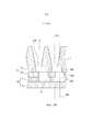
Фиг.1 - перспективный вид, схематично показывающий
конфигурацию антенны 100;Figure 1 is a perspective view schematically showing
Фиг.2A - вид сверху, схематично показывающий конфигурацию антенны 100;2A is a plan view schematically showing the configuration of an
Фиг.2B - вид сверху, схематично показывающий размещение рупорных антенн 51-53;2B is a plan view schematically showing the placement of horn antennas 51-53;
Фиг.3A - увеличенный вид в разрезе, схематично показывающий конфигурацию поперечного разреза в антенне 100, взятого вдоль линии IIIA-IIIA, показанной на фиг.2А;FIG. 3A is an enlarged sectional view schematically showing a cross-sectional configuration in an
Фиг.3B - увеличенный вид в разрезе, схематично показывающий конфигурацию поперечного разреза антенны 101, взятого вдоль линии IIIB-IIIB, показанной на фиг.2А;FIG. 3B is an enlarged sectional view schematically showing a cross-sectional configuration of an antenna 101 taken along line IIIB-IIIB shown in FIG. 2A;
Фиг.4 - схема, схематично показывающая конфигурацию слоя 3 волновода и соединительного слоя 2 при виде со стороны нижнего слоя 4; и4 is a diagram schematically showing the configuration of the
Фиг.5 - график, показывающий характеристики излучения радиоволн антенны 100.5 is a graph showing the radiation characteristics of the radio waves of the
Подробное описание изобретенияDETAILED DESCRIPTION OF THE INVENTION
Примерные варианты осуществления настоящего изобретения будут описаны ниже со ссылкой на чертежи. На чертежах одинаковые элементы обозначены одинаковыми ссылочными позициями, и, таким образом, их повторное описание, если оно не является необходимым, не приводится.Exemplary embodiments of the present invention will be described below with reference to the drawings. In the drawings, the same elements are denoted by the same reference position, and thus, their repeated description, if it is not necessary, is not given.
Первый примерный вариант осуществленияFirst Exemplary Embodiment
Сначала будет описана антенна 100 согласно примерному варианту осуществления. На фиг.1 представлен перспективный вид, схематично показывающий конфигурацию антенны 100, причем антенна 100 включает в себя слой 1 антенны, соединительный слой 2, слой 3 волновода и нижний слой 4, при этом слой 1 антенны, соединительный слой 2, слой 3 волновода и нижний слой 4 выполнены по отдельности, например, из металла, и слой 3 волновода и нижний слой 4 образуют слой 10 фидерного тракта.First, an
На фиг.2А представлен вид сверху, схематично показывающий конфигурацию антенны 100. Рупорные антенны 5, каждая из которых имеет форму прямоугольной пирамиды, расположены в шахматном порядке в слое 1 антенны. В дальнейшем рупорные антенны также упоминаются просто как антенные элементы, при этом каждая рупорная антенна в соседних рядах расположена со смещением. В этом примерном варианте осуществления рупорные антенны 5, которые размещаются в ряду B, показанном на фиг.2А, смещены в направлении C (которое также упоминается как первое направление) относительно рупорных антенн 5, размещенных в ряду А, показанном на фиг.2А. Кроме того, так как рупорные антенны 5 размещаются в шахматном порядке, центр каждой рупорной антенны 5 в ряду A находится на одинаковом расстоянии от центра между двумя рупорными антеннами 5 в ряду B, который примыкает в направлении D к ряду A.2A is a plan view schematically showing the configuration of the
Следует отметить, что направление C представляет собой направление, параллельное основной поверхности слоя 1 антенны, и направление D (которое также упоминается как второе направление) представляет собой направление, которое параллельно основной поверхности слоя 1 антенны и перпендикулярно к направлению C.It should be noted that direction C is a direction parallel to the main surface of the antenna layer 1, and direction D (which is also referred to as the second direction) is a direction that is parallel to the main surface of the antenna layer 1 and perpendicular to direction C.
Рассмотрим теперь три соседних рупорных антенны 51-53. На фиг.2B представлен вид сверху, схематично показывающий размещение рупорных антенн 51-53. При упрощенном рассмотрении вышеупомянутого смещения значение смещения можно понять следующим образом. Здесь будет описан случай, когда центры рупорных антенн 51 и 52 выровнены в направлении C. В этом случае рупорная антенна 53 расположена отдельно от рупорной антенны 51 в направлении D. Можно понять, что рупорные антенны 51 и 53 размещаются таким образом, чтобы центры рупорных антенн 51 и 53 не были выровнены в направлении D.Consider now three adjacent horn antennas 51-53. 2B is a plan view schematically showing the placement of horn antennas 51-53. In a simplified discussion of the aforementioned bias, the bias value can be understood as follows. Here, a case will be described where the centers of the
Далее будет описана конфигурация антенны 100 в разрезе. На фиг.3A представлен увеличенный вид в разрезе, схематично показывающий конфигурацию поперечного разреза антенны 100, взятого вдоль линии IIIA-IIIA (фиг.2A). На фиг.3B представлен увеличенный вид в разрезе, схематично показывающий конфигурацию антенны 100 в разрезе, взятом вдоль линии IIIB-IIIB (фиг.2A). Слой 1 антенны расположен на соединительном слое 2, соединительный слой 2 расположен на слое 3 волновода, слой 3 волновода расположен на нижнем слое 4. Слой 1 антенны, соединительный слой 2, слой 3 волновода и нижний слой 4 можно расположить друг над другом с помощью различных способов соединения, таких как привинчивание и приклеивание с использованием клея.Next, a sectional view of an
Соединительный слой 2 образован из верхнего слоя 21 соединительного слоя и нижнего слоя 22 соединительного слоя. В верхнем слое 21 соединительного слоя образованы верхние волноводы, которые проникают в верхний слой 21 соединительного слоя. По линии IIIA-IIIA верхний волновод 23А, который продолжается в направлении C, как показано в фиг.3A, сформирован в верхнем слое 21 соединительного слоя. Правый конец верхнего волновода 23А соединен с нижним концом соответствующей рупорной антенны 5 на конце 27А соединения (который также упоминается как третий конец соединения). По линии IIIB-IIIB верхний волновод 23B, который продолжается в направлении C, как показано в фиг.3B, образован в верхнем слое 21 соединительного слоя, левый конец верхнего волновода 23В соединен с нижним концом соответствующей рупорной антенны 5 на конце 27В соединения (который также упоминается как четвертый конец соединения). То есть можно понять, что верхний волновод 23А по линии IIIA-IIIA соединен с соответствующей рупорной антенной 5 в направлении, противоположном верхнему волноводу 23В, по линии IIIB-IIIB.The connecting
В нижнем слое 22 соединительного слоя образованы нижние волноводы, которые проникают в нижний слой 22 соединительного слоя. По линии IIIA-IIIA нижний волновод 24А, который продолжается в направлении C, как показано в фиг.3A, образован в нижнем слое 22 соединительного слоя. Правый конец нижнего волновода 24А соединен с левым концом соответствующего верхнего волновода 23А. По линии IIIB-IIIB нижний волновод 24В, который продолжается в направлении C, как показано в фиг.3В, образован в нижнем слое 22 соединительного слоя. Левый конец нижнего волновода 24В соединен с правым концом верхнего волновода 23В.In the
Каждый из верхнего волновода 23А и нижнего волновода 24А также упоминается как второй волновод. Каждый из верхнего волновода 24В и нижнего волновода 24В также упоминается как третий волновод.Each of the
В слое 3 волновода образован волновод 31 (который также упоминается как первый волновод), который проходит в слой 3 волновода. Волновод 31 соединен нижним концом нижнего волновода 24А и нижним концом нижнего волновода 24В.A waveguide 31 (also referred to as a first waveguide) is formed in the
Следует отметить, что центр 26А конца 25А соединения (который также упоминается как первый конец соединения), который соединяет нижний волновод 24А и волновод 31 друг с другом, и центр 26В конца 25В соединения (который также упоминается как второй конец соединения), который соединяет нижний волновод 24В и волновод 31 друг с другом, образованы в положениях, где отсутствует смещение в отличие от рупорных антенн 5. В частности, можно понять, что на базе центра 26А конца 25А соединения, по линии IIIA-IIIA, радиоволны распространяются в направлении вверх вправо из волновода 31 в нижний конец рупорной антенны 5 через нижний волновод 24А и верхний волновод 23А, можно также понять, что на базе центра 26B конца 25B соединения по линии IIIB-IIIB радиоволны распространяются в направлении вверх влево из волновода 31 в нижнем конце рупорной антенны 5 через нижний волновод 24B и верхний волновод 23В.It should be noted that the
С помощью этой конфигурации даже в том случае, если волновод 31 образован без учета смещения, расстояния от волновода 31 до рупорных антенн 5, которые смещены по линии IIIA-IIIA и линии IIIB-IIIB, могут быть равны только за счет смещения направлений волноводов верхнего волновода и нижнего волновода в противоположных направлениях на одинаковое значение ΔD (которое также упоминается как первое значение), тем самым позволяя направлять радиоволны, не приводя к какой-либо разности фаз.With this configuration, even if the
Далее будет описана конфигурация слоя 3 волновода. На фиг.4 представлена схема, схематично показывающая конфигурацию каждого из слоя 3 волновода и соединительного слоя 2 при виде со стороны нижнего слоя 4. В нижнем слое 4 образован вход волновода, который проходит в нижний слой 4 (не показан), вход волновода связан с волноводом 31 в местоположении 32, показанном на фиг.4. Соответственно, радиоволны вводятся в волновод 31 через вход волновода.Next, the configuration of the
В слое 3 волновода образован волновод 31 в качестве волновода, имеющего ответвления, таким образом, чтобы расстояния от участка, связанного с входом волновода (то есть местоположение 32, показанное на фиг.4) с концом 25А соединения и концом 25B соединения, были равны друг другу. Другими словами, радиоволны распространяются извне в конец 25А соединения и конец 25B соединения через вход волновода с одинаковой фазой.In
Далее будут описаны характеристики излучения радиоволн антенны 100. На фиг.5 представлен график, показывающий характеристики излучения радиоволн антенны 100. Как показано на фиг.5, характеристики излучения радиоволн антенны 100 показаны сплошной линией L1. В качестве сравнительных примеров, характеристики излучения радиоволн антенны, в которой рупорная антенна расположена в виде квадратной решетки без обеспечения смещения, как раскрыто в патентной литературе 1, показаны пунктирной линией L2, и стандарты КЛАСС 2 ETSI (Европейский институт телекоммуникационных стандартов) показаны жирной линией L3.Next, radiation characteristics of the radio waves of the
По горизонтальной оси отложен азимут поверхности, взятой вдоль линии V-V, показанный на фиг.2А, в качестве поверхности наблюдения. Следует отметить, что передняя сторона антенны 100 обозначена 0. По вертикальной оси отложен коэффициент направленного действия.The horizontal axis represents the azimuth of the surface taken along the line V-V, shown in figa, as the observation surface. It should be noted that the front side of the
Как показано в фиг.5, следует понимать, что в сравнительном примере (L2) имеют место боковые лепестки с большим коэффициентом направленного действия, при этом лепестки выходят за рамки стандарта КЛАССА 2 ETSI (Европейского института телекоммуникационных стандартов) (L3). То есть, как упомянуто выше, боковые лепестки в сравнительном примере (L2) недостаточно подавляются.As shown in figure 5, it should be understood that in the comparative example (L2) there are side lobes with a large coefficient of directional action, while the lobes are outside the scope of the ETSI CLASS 2 (European Telecommunications Standards Institute) standard (L3). That is, as mentioned above, the side lobes in the comparative example (L2) are not sufficiently suppressed.
С другой стороны, в характеристиках излучения радиоволн (L1) антенны 100 боковые лепестки подавляются достаточным образом, и, таким образом, можно достичь характеристики излучения радиоволн, которые удовлетворяют стандартам (L3) КЛАССА 2 ETSI (Европейского института телекоммуникационных стандартов). То есть можно понять, что рупорные антенны 5 размещаются со смещением, как в конфигурации настоящего изобретения, тем самым получая антенну, имеющую характеристики излучения радиоволн, в которых боковые лепестки подавляются достаточным образом.On the other hand, in the emission characteristics of the radio waves (L1) of the
В вышеописанном сравнительном примере (L2) для того, чтобы подавить боковые лепестки, необходимо уменьшить размер отверстия каждой рупорной антенны таким образом, чтобы он был меньше длины волны излучаемой волны (например, миллиметровой волны), и увеличить плотность размещения рупорных антенн. Однако в этом случае конструкции рупорных антенн и волноводов, которые ведут в рупорные антенны, становятся меньше, что затрудняет изготовление антенн и волноводов и приводит к увеличению стоимости антенны.In the above comparative example (L2), in order to suppress the side lobes, it is necessary to reduce the hole size of each horn antenna so that it is less than the wavelength of the emitted wave (for example, a millimeter wave), and increase the density of the horn antennas. However, in this case, the design of the horn antennas and waveguides that lead to the horn antennas becomes smaller, which complicates the manufacture of antennas and waveguides and leads to an increase in the cost of the antenna.
С другой стороны, в конфигурации настоящего изобретения, боковые лепестки можно подавить путем размещения рупорных антенн, которое избавляет от необходимости увеличивать плотность размещения рупорных антенн. Поэтому в этой конфигурации размер отверстия (длина стороны отверстия) каждой из рупорных антенн 5 можно установить равным или более чем длина волны излучаемой радиоволны (например, миллиметровой волны). Однако, принимая во внимание удобство реального использования антенны и легкость изготовления антенны, размер отверстия (длина стороны отверстия) каждой из рупорных антенн 5 желательно устанавливать таким образом, чтобы он был равен или меньше чем четверть длины волны излучаемой волны. Однако это не предполагает исключения случая, когда размер отверстия (длина стороны отверстия) каждой из рупорных антенн 5 устанавливается равным или более чем четверть длины волны излучаемой волны.On the other hand, in the configuration of the present invention, the side lobes can be suppressed by placing horn antennas, which eliminates the need to increase the density of the horn antennas. Therefore, in this configuration, the hole size (hole side length) of each of the
Поэтому согласно конфигурации настоящего изобретения конструкции рупорных антенн и волноводов, ведущих к рупорным антеннам, можно легко изготовить и, таким образом, можно производить антенну с низкой ценой.Therefore, according to the configuration of the present invention, the designs of the horn antennas and waveguides leading to the horn antennas can be easily manufactured, and thus, a low cost antenna can be manufactured.
Настоящее изобретение не ограничивается вышеупомянутыми примерными вариантами осуществления и может быть изменено соответствующим образом без отклонения от объема изобретения. Например, рупорные антенны были описаны выше в виде антенных элементов, но они являются только примером. Например, можно также использовать другие антенные элементы, такие как линзовые антенны и диэлектрические стержневые антенны. Кроме того, выше были описаны рупорные антенны, каждая из которых выполнена в форме прямоугольной пирамиды, но это является только примером. Например, рупорные антенны, выполненные с другими пирамидальными формами, такими как форма конуса, форма эллиптического конуса и форма шестиугольной пирамиды, можно также использовать до тех пор, пока не будет получен желаемый коэффициент направленного действия. Помимо пирамидальной формы можно также использовать и цилиндрическую форму.The present invention is not limited to the aforementioned exemplary embodiments, and may be modified accordingly without departing from the scope of the invention. For example, horn antennas have been described above as antenna elements, but they are only an example. For example, other antenna elements, such as lens antennas and dielectric rod antennas, can also be used. In addition, horn antennas have been described above, each of which is in the shape of a rectangular pyramid, but this is only an example. For example, horn antennas made with other pyramidal shapes, such as a cone shape, an elliptical cone shape, and a hexagonal pyramid shape, can also be used until the desired directional coefficient is obtained. In addition to the pyramidal shape, a cylindrical shape can also be used.
Волноводы (верхний волновод 23А, нижний волновод 24А, верхний волновод 230 и нижний волновод 240), которые имеют форму четырехколенного коленчатого вала и соединяют рупорные антенны 5 со слоем 3 волновода, были описаны выше, но они являются только примером. Например, волноводы, которые соединяют рупорные антенны 5 со слоем 3 волновода, могут иметь форму коленчатого вала с произвольным числом колен, отличным от четырех, до тех пор, пока потери на отражение радиоволн не будут находиться в допустимом диапазоне. Альтернативно, волноводы, которые соединяют рупорные антенны 5 со слоем 3 волновода, могут представлять собой гладкие коаксиальные линии, имеющие форму, отличную от формы коленчатого вала до тех пор, пока потери на отражение радиоволн не будут находиться в пределах допустимого диапазона.The waveguides (
Размещение рупорных антенн 5 было описано выше только в качестве примера. Вместо размещения рупорных антенн 5 строго в шахматном порядке рупорные антенны 5 можно разместить, например, с произвольным смещением между размещением в шахматном порядке и размещением в виде квадратной решетки. Рупорные антенны 5 необязательно должны размещаться через одинаковые промежутки по всей поверхности слоя 1 антенны, и может присутствовать множество областей, в которых рупорные антенны смещены различными способами. Другими словами, антенна 100 включает в себя область, в которой рупорные антенны 5 размещаются с искусственным смещением, чтобы предотвратить размещение рупорных антенн в виде квадратной решетки, тем самым позволяя подавить боковые лепестки излучаемой волны.The placement of the
Слой 1 антенны, верхний слой 21 соединительного слоя, верхний слой 22 соединительного слоя, слой 3 волновода и нижний слой 4 (которые образуют слой 10 фидерного тракта) можно выполнить как единое целое при условии, что их можно изготовить. Например, в случае изготовления слоев с помощью литья, верхний слой 21 соединительного слоя и нижний слой 22 соединительного слоя можно выполнить как единое целое со слоем 1 антенны, или верхний слой 21 соединительного слоя можно выполнить как единое целое со слоем 1 антенны, верхний слой 21 соединительного слоя и нижний слой 22 соединительного слоя можно выполнить как единое целое со слоем 3 волновода, или нижний слой 22 соединительного слоя можно выполнить как единое целое со слоем 3 волновода.The antenna layer 1, the
Слой 1 антенны, соединительный слой 2, слой 3 волновода и нижний слой 4 можно выполнить не только из металла, но также и из диэлектрического материала, такого как смола, поверхность которой покрывается проводящим материалом, таким как металл. В случае использования смолы антенну можно легко изготовить путем литья под давлением и т.п.The antenna layer 1, the connecting
Случай, где вход волновода образован в нижнем слое 4, был описан выше только в качестве примера, вход волновода можно сформировать, например, в слое 3 волновода.The case where the waveguide input is formed in the
Хотя настоящее изобретение было описано выше со ссылкой на примерные варианты осуществления, настоящее изобретение не ограничено вышеописанными примерными вариантами осуществления. Конфигурацию и детали настоящего изобретения можно модифицировать различными способами, которые понятны специалистам в данной области техники в пределах объема настоящего изобретения.Although the present invention has been described above with reference to exemplary embodiments, the present invention is not limited to the above exemplary embodiments. The configuration and details of the present invention can be modified in various ways that are understood by those skilled in the art within the scope of the present invention.
Данная заявка основана на и испрашивает приоритет Японской патентной заявки №2013-8172, поданной 21 января 2013 года, раскрытие которой включено сюда во всей своей полноте путем ссылки.This application is based on and claims the priority of Japanese Patent Application No. 2013-8172, filed January 21, 2013, the disclosure of which is incorporated herein in its entirety by reference.
Перечень ссылочных позицийList of Reference Items
100 - АНТЕННА100 - ANTENNA
1 - СЛОЙ АНТЕННЫ1 - ANTENNA LAYER
2 - СОЕДИНИТЕЛЬНЫЙ СЛОЙ2 - CONNECTING LAYER
3 - СЛОЙ ВОЛНОВОДА3 - LAYER OF A WAVEGUIDE
4 - НИЖНИЙ СЛОЙ4 - LOWER LAYER
5, 51-53 - РУПОРНЫЕ АНТЕННЫ5, 51-53 - HORN ANTENNA
10 - СЛОЙ ФИДЕРНОГО ТРАКТА10 - FEDERAL LAYER LAYER
21 - ВЕРХНИЙ СЛОЙ СОЕДИНИТЕЛЬНОГО СЛОЯ21 - TOP LAYER OF THE CONNECTING LAYER
22 - НИЖНИЙ СЛОЙ СОЕДИНИТЕЛЬНОГО СЛОЯ22 - LOWER LAYER OF THE CONNECTING LAYER
23А - ВЕРХНИЙ ВОЛНОВОД23A - UPPER WAVEGUIDE
238 - ВЕРХНИЙ ВОЛНОВОД238 - UPPER WAVEGUIDE
24А - НИЖНИЙ ВОЛНОВОД24A - LOWER WAVEGUIDE
248 - НИЖНИЙ ВОЛНОВОД248 - LOWER WAVEGUIDE
31 - ВОЛНОВОД31 - WAVEGUIDE
25А - КОНЕЦ СОЕДИНЕНИЯ25A - END OF CONNECTION
25B - КОНЕЦ СОЕДИНЕНИЯ25B - END OF CONNECTION
26А - ЦЕНТР КОНЦА 25А СОЕДИНЕНИЯ26A -
26B - ЦЕНТР КОНЦА 25B СОЕДИНЕНИЯ26B -
27А - КОНЕЦ СОЕДИНЕНИЯ27A - END OF CONNECTION
27B - КОНЕЦ СОЕДИНЕНИЯ27B - END OF CONNECTION
Claims (19)
Translated fromRussianApplications Claiming Priority (3)
| Application Number | Priority Date | Filing Date | Title |
|---|---|---|---|
| JP2013-008172 | 2013-01-21 | ||
| JP2013008172 | 2013-01-21 | ||
| PCT/JP2013/007074WO2014111996A1 (en) | 2013-01-21 | 2013-12-03 | Antenna |
Publications (1)
| Publication Number | Publication Date |
|---|---|
| RU2607769C1true RU2607769C1 (en) | 2017-01-10 |
Family
ID=51209125
Family Applications (1)
| Application Number | Title | Priority Date | Filing Date |
|---|---|---|---|
| RU2015135368ARU2607769C1 (en) | 2013-01-21 | 2013-12-03 | Antenna |
Country Status (8)
| Country | Link |
|---|---|
| US (1) | US9692117B2 (en) |
| EP (1) | EP2947717A4 (en) |
| CN (1) | CN104937777A (en) |
| MX (1) | MX2015009202A (en) |
| PH (1) | PH12015501564A1 (en) |
| RU (1) | RU2607769C1 (en) |
| WO (1) | WO2014111996A1 (en) |
| ZA (1) | ZA201505072B (en) |
Cited By (3)
| Publication number | Priority date | Publication date | Assignee | Title |
|---|---|---|---|---|
| RU175123U1 (en)* | 2017-03-20 | 2017-11-21 | Акционерное общество "Научно-исследовательский институт Приборостроения имени В.В. Тихомирова" | Panel of waveguide-horn emitters |
| RU195879U1 (en)* | 2019-11-27 | 2020-02-07 | Акционерное общество "Научно-исследовательский институт Приборостроения имени В.В. Тихомирова" | Waveguide-horn radiator module |
| RU2723980C1 (en)* | 2019-12-06 | 2020-06-18 | Публичное акционерное общество "Радиофизика" | Horn radiator for antenna arrays with circular polarization |
Families Citing this family (134)
| Publication number | Priority date | Publication date | Assignee | Title |
|---|---|---|---|---|
| US9525524B2 (en) | 2013-05-31 | 2016-12-20 | At&T Intellectual Property I, L.P. | Remote distributed antenna system |
| US9999038B2 (en) | 2013-05-31 | 2018-06-12 | At&T Intellectual Property I, L.P. | Remote distributed antenna system |
| US8897697B1 (en) | 2013-11-06 | 2014-11-25 | At&T Intellectual Property I, Lp | Millimeter-wave surface-wave communications |
| US9768833B2 (en) | 2014-09-15 | 2017-09-19 | At&T Intellectual Property I, L.P. | Method and apparatus for sensing a condition in a transmission medium of electromagnetic waves |
| US10063280B2 (en) | 2014-09-17 | 2018-08-28 | At&T Intellectual Property I, L.P. | Monitoring and mitigating conditions in a communication network |
| US9615269B2 (en) | 2014-10-02 | 2017-04-04 | At&T Intellectual Property I, L.P. | Method and apparatus that provides fault tolerance in a communication network |
| US9685992B2 (en) | 2014-10-03 | 2017-06-20 | At&T Intellectual Property I, L.P. | Circuit panel network and methods thereof |
| US9503189B2 (en) | 2014-10-10 | 2016-11-22 | At&T Intellectual Property I, L.P. | Method and apparatus for arranging communication sessions in a communication system |
| US9973299B2 (en) | 2014-10-14 | 2018-05-15 | At&T Intellectual Property I, L.P. | Method and apparatus for adjusting a mode of communication in a communication network |
| US9312919B1 (en) | 2014-10-21 | 2016-04-12 | At&T Intellectual Property I, Lp | Transmission device with impairment compensation and methods for use therewith |
| US9769020B2 (en) | 2014-10-21 | 2017-09-19 | At&T Intellectual Property I, L.P. | Method and apparatus for responding to events affecting communications in a communication network |
| US9627768B2 (en) | 2014-10-21 | 2017-04-18 | At&T Intellectual Property I, L.P. | Guided-wave transmission device with non-fundamental mode propagation and methods for use therewith |
| US9577306B2 (en) | 2014-10-21 | 2017-02-21 | At&T Intellectual Property I, L.P. | Guided-wave transmission device and methods for use therewith |
| US9653770B2 (en) | 2014-10-21 | 2017-05-16 | At&T Intellectual Property I, L.P. | Guided wave coupler, coupling module and methods for use therewith |
| US9780834B2 (en) | 2014-10-21 | 2017-10-03 | At&T Intellectual Property I, L.P. | Method and apparatus for transmitting electromagnetic waves |
| US9544006B2 (en) | 2014-11-20 | 2017-01-10 | At&T Intellectual Property I, L.P. | Transmission device with mode division multiplexing and methods for use therewith |
| US9461706B1 (en) | 2015-07-31 | 2016-10-04 | At&T Intellectual Property I, Lp | Method and apparatus for exchanging communication signals |
| US10243784B2 (en) | 2014-11-20 | 2019-03-26 | At&T Intellectual Property I, L.P. | System for generating topology information and methods thereof |
| US9800327B2 (en) | 2014-11-20 | 2017-10-24 | At&T Intellectual Property I, L.P. | Apparatus for controlling operations of a communication device and methods thereof |
| US10340573B2 (en) | 2016-10-26 | 2019-07-02 | At&T Intellectual Property I, L.P. | Launcher with cylindrical coupling device and methods for use therewith |
| US10009067B2 (en) | 2014-12-04 | 2018-06-26 | At&T Intellectual Property I, L.P. | Method and apparatus for configuring a communication interface |
| US9954287B2 (en) | 2014-11-20 | 2018-04-24 | At&T Intellectual Property I, L.P. | Apparatus for converting wireless signals and electromagnetic waves and methods thereof |
| US9742462B2 (en) | 2014-12-04 | 2017-08-22 | At&T Intellectual Property I, L.P. | Transmission medium and communication interfaces and methods for use therewith |
| US9997819B2 (en) | 2015-06-09 | 2018-06-12 | At&T Intellectual Property I, L.P. | Transmission medium and method for facilitating propagation of electromagnetic waves via a core |
| US9876570B2 (en) | 2015-02-20 | 2018-01-23 | At&T Intellectual Property I, Lp | Guided-wave transmission device with non-fundamental mode propagation and methods for use therewith |
| US9749013B2 (en) | 2015-03-17 | 2017-08-29 | At&T Intellectual Property I, L.P. | Method and apparatus for reducing attenuation of electromagnetic waves guided by a transmission medium |
| US10224981B2 (en) | 2015-04-24 | 2019-03-05 | At&T Intellectual Property I, Lp | Passive electrical coupling device and methods for use therewith |
| US9705561B2 (en) | 2015-04-24 | 2017-07-11 | At&T Intellectual Property I, L.P. | Directional coupling device and methods for use therewith |
| US9793954B2 (en) | 2015-04-28 | 2017-10-17 | At&T Intellectual Property I, L.P. | Magnetic coupling device and methods for use therewith |
| US9748626B2 (en) | 2015-05-14 | 2017-08-29 | At&T Intellectual Property I, L.P. | Plurality of cables having different cross-sectional shapes which are bundled together to form a transmission medium |
| US9490869B1 (en) | 2015-05-14 | 2016-11-08 | At&T Intellectual Property I, L.P. | Transmission medium having multiple cores and methods for use therewith |
| US9871282B2 (en) | 2015-05-14 | 2018-01-16 | At&T Intellectual Property I, L.P. | At least one transmission medium having a dielectric surface that is covered at least in part by a second dielectric |
| US10650940B2 (en) | 2015-05-15 | 2020-05-12 | At&T Intellectual Property I, L.P. | Transmission medium having a conductive material and methods for use therewith |
| US10361476B2 (en)* | 2015-05-26 | 2019-07-23 | Qualcomm Incorporated | Antenna structures for wireless communications |
| US9917341B2 (en) | 2015-05-27 | 2018-03-13 | At&T Intellectual Property I, L.P. | Apparatus and method for launching electromagnetic waves and for modifying radial dimensions of the propagating electromagnetic waves |
| US9912381B2 (en) | 2015-06-03 | 2018-03-06 | At&T Intellectual Property I, Lp | Network termination and methods for use therewith |
| US10812174B2 (en) | 2015-06-03 | 2020-10-20 | At&T Intellectual Property I, L.P. | Client node device and methods for use therewith |
| US9866309B2 (en) | 2015-06-03 | 2018-01-09 | At&T Intellectual Property I, Lp | Host node device and methods for use therewith |
| EP3306747A4 (en)* | 2015-06-03 | 2019-01-02 | Mitsubishi Electric Corporation | Horn antenna |
| US9913139B2 (en) | 2015-06-09 | 2018-03-06 | At&T Intellectual Property I, L.P. | Signal fingerprinting for authentication of communicating devices |
| US9820146B2 (en) | 2015-06-12 | 2017-11-14 | At&T Intellectual Property I, L.P. | Method and apparatus for authentication and identity management of communicating devices |
| US9667317B2 (en) | 2015-06-15 | 2017-05-30 | At&T Intellectual Property I, L.P. | Method and apparatus for providing security using network traffic adjustments |
| US9865911B2 (en) | 2015-06-25 | 2018-01-09 | At&T Intellectual Property I, L.P. | Waveguide system for slot radiating first electromagnetic waves that are combined into a non-fundamental wave mode second electromagnetic wave on a transmission medium |
| US9640850B2 (en) | 2015-06-25 | 2017-05-02 | At&T Intellectual Property I, L.P. | Methods and apparatus for inducing a non-fundamental wave mode on a transmission medium |
| US9509415B1 (en) | 2015-06-25 | 2016-11-29 | At&T Intellectual Property I, L.P. | Methods and apparatus for inducing a fundamental wave mode on a transmission medium |
| US9628116B2 (en) | 2015-07-14 | 2017-04-18 | At&T Intellectual Property I, L.P. | Apparatus and methods for transmitting wireless signals |
| US9722318B2 (en) | 2015-07-14 | 2017-08-01 | At&T Intellectual Property I, L.P. | Method and apparatus for coupling an antenna to a device |
| US9882257B2 (en) | 2015-07-14 | 2018-01-30 | At&T Intellectual Property I, L.P. | Method and apparatus for launching a wave mode that mitigates interference |
| US9847566B2 (en) | 2015-07-14 | 2017-12-19 | At&T Intellectual Property I, L.P. | Method and apparatus for adjusting a field of a signal to mitigate interference |
| US10044409B2 (en) | 2015-07-14 | 2018-08-07 | At&T Intellectual Property I, L.P. | Transmission medium and methods for use therewith |
| US10205655B2 (en) | 2015-07-14 | 2019-02-12 | At&T Intellectual Property I, L.P. | Apparatus and methods for communicating utilizing an antenna array and multiple communication paths |
| US9853342B2 (en) | 2015-07-14 | 2017-12-26 | At&T Intellectual Property I, L.P. | Dielectric transmission medium connector and methods for use therewith |
| US10320586B2 (en) | 2015-07-14 | 2019-06-11 | At&T Intellectual Property I, L.P. | Apparatus and methods for generating non-interfering electromagnetic waves on an insulated transmission medium |
| US10148016B2 (en) | 2015-07-14 | 2018-12-04 | At&T Intellectual Property I, L.P. | Apparatus and methods for communicating utilizing an antenna array |
| US9793951B2 (en) | 2015-07-15 | 2017-10-17 | At&T Intellectual Property I, L.P. | Method and apparatus for launching a wave mode that mitigates interference |
| US10090606B2 (en) | 2015-07-15 | 2018-10-02 | At&T Intellectual Property I, L.P. | Antenna system with dielectric array and methods for use therewith |
| US9912027B2 (en) | 2015-07-23 | 2018-03-06 | At&T Intellectual Property I, L.P. | Method and apparatus for exchanging communication signals |
| US9948333B2 (en) | 2015-07-23 | 2018-04-17 | At&T Intellectual Property I, L.P. | Method and apparatus for wireless communications to mitigate interference |
| US9871283B2 (en) | 2015-07-23 | 2018-01-16 | At&T Intellectual Property I, Lp | Transmission medium having a dielectric core comprised of plural members connected by a ball and socket configuration |
| US9749053B2 (en) | 2015-07-23 | 2017-08-29 | At&T Intellectual Property I, L.P. | Node device, repeater and methods for use therewith |
| US9967173B2 (en) | 2015-07-31 | 2018-05-08 | At&T Intellectual Property I, L.P. | Method and apparatus for authentication and identity management of communicating devices |
| US9735833B2 (en) | 2015-07-31 | 2017-08-15 | At&T Intellectual Property I, L.P. | Method and apparatus for communications management in a neighborhood network |
| US10297924B2 (en)* | 2015-08-27 | 2019-05-21 | Nidec Corporation | Radar antenna unit and radar device |
| US9904535B2 (en) | 2015-09-14 | 2018-02-27 | At&T Intellectual Property I, L.P. | Method and apparatus for distributing software |
| US9769128B2 (en) | 2015-09-28 | 2017-09-19 | At&T Intellectual Property I, L.P. | Method and apparatus for encryption of communications over a network |
| US9729197B2 (en) | 2015-10-01 | 2017-08-08 | At&T Intellectual Property I, L.P. | Method and apparatus for communicating network management traffic over a network |
| US9876264B2 (en) | 2015-10-02 | 2018-01-23 | At&T Intellectual Property I, Lp | Communication system, guided wave switch and methods for use therewith |
| US10355367B2 (en) | 2015-10-16 | 2019-07-16 | At&T Intellectual Property I, L.P. | Antenna structure for exchanging wireless signals |
| US9860075B1 (en) | 2016-08-26 | 2018-01-02 | At&T Intellectual Property I, L.P. | Method and communication node for broadband distribution |
| JP6723133B2 (en)* | 2016-10-04 | 2020-07-15 | 日立オートモティブシステムズ株式会社 | Antenna, sensor and in-vehicle system |
| US10135147B2 (en) | 2016-10-18 | 2018-11-20 | At&T Intellectual Property I, L.P. | Apparatus and methods for launching guided waves via an antenna |
| US10135146B2 (en) | 2016-10-18 | 2018-11-20 | At&T Intellectual Property I, L.P. | Apparatus and methods for launching guided waves via circuits |
| US10340600B2 (en) | 2016-10-18 | 2019-07-02 | At&T Intellectual Property I, L.P. | Apparatus and methods for launching guided waves via plural waveguide systems |
| US10811767B2 (en) | 2016-10-21 | 2020-10-20 | At&T Intellectual Property I, L.P. | System and dielectric antenna with convex dielectric radome |
| US10374316B2 (en) | 2016-10-21 | 2019-08-06 | At&T Intellectual Property I, L.P. | System and dielectric antenna with non-uniform dielectric |
| US9991580B2 (en) | 2016-10-21 | 2018-06-05 | At&T Intellectual Property I, L.P. | Launcher and coupling system for guided wave mode cancellation |
| US9876605B1 (en) | 2016-10-21 | 2018-01-23 | At&T Intellectual Property I, L.P. | Launcher and coupling system to support desired guided wave mode |
| US10312567B2 (en) | 2016-10-26 | 2019-06-04 | At&T Intellectual Property I, L.P. | Launcher with planar strip antenna and methods for use therewith |
| US10291334B2 (en) | 2016-11-03 | 2019-05-14 | At&T Intellectual Property I, L.P. | System for detecting a fault in a communication system |
| US10498044B2 (en) | 2016-11-03 | 2019-12-03 | At&T Intellectual Property I, L.P. | Apparatus for configuring a surface of an antenna |
| US10225025B2 (en) | 2016-11-03 | 2019-03-05 | At&T Intellectual Property I, L.P. | Method and apparatus for detecting a fault in a communication system |
| US10224634B2 (en) | 2016-11-03 | 2019-03-05 | At&T Intellectual Property I, L.P. | Methods and apparatus for adjusting an operational characteristic of an antenna |
| US10340601B2 (en) | 2016-11-23 | 2019-07-02 | At&T Intellectual Property I, L.P. | Multi-antenna system and methods for use therewith |
| US10535928B2 (en) | 2016-11-23 | 2020-01-14 | At&T Intellectual Property I, L.P. | Antenna system and methods for use therewith |
| US10090594B2 (en) | 2016-11-23 | 2018-10-02 | At&T Intellectual Property I, L.P. | Antenna system having structural configurations for assembly |
| US10178445B2 (en) | 2016-11-23 | 2019-01-08 | At&T Intellectual Property I, L.P. | Methods, devices, and systems for load balancing between a plurality of waveguides |
| US10340603B2 (en) | 2016-11-23 | 2019-07-02 | At&T Intellectual Property I, L.P. | Antenna system having shielded structural configurations for assembly |
| US10361489B2 (en) | 2016-12-01 | 2019-07-23 | At&T Intellectual Property I, L.P. | Dielectric dish antenna system and methods for use therewith |
| US10305190B2 (en) | 2016-12-01 | 2019-05-28 | At&T Intellectual Property I, L.P. | Reflecting dielectric antenna system and methods for use therewith |
| US10755542B2 (en) | 2016-12-06 | 2020-08-25 | At&T Intellectual Property I, L.P. | Method and apparatus for surveillance via guided wave communication |
| US10819035B2 (en) | 2016-12-06 | 2020-10-27 | At&T Intellectual Property I, L.P. | Launcher with helical antenna and methods for use therewith |
| US10382976B2 (en) | 2016-12-06 | 2019-08-13 | At&T Intellectual Property I, L.P. | Method and apparatus for managing wireless communications based on communication paths and network device positions |
| US9927517B1 (en) | 2016-12-06 | 2018-03-27 | At&T Intellectual Property I, L.P. | Apparatus and methods for sensing rainfall |
| US10727599B2 (en) | 2016-12-06 | 2020-07-28 | At&T Intellectual Property I, L.P. | Launcher with slot antenna and methods for use therewith |
| US10326494B2 (en) | 2016-12-06 | 2019-06-18 | At&T Intellectual Property I, L.P. | Apparatus for measurement de-embedding and methods for use therewith |
| US10694379B2 (en) | 2016-12-06 | 2020-06-23 | At&T Intellectual Property I, L.P. | Waveguide system with device-based authentication and methods for use therewith |
| US10637149B2 (en) | 2016-12-06 | 2020-04-28 | At&T Intellectual Property I, L.P. | Injection molded dielectric antenna and methods for use therewith |
| US10439675B2 (en) | 2016-12-06 | 2019-10-08 | At&T Intellectual Property I, L.P. | Method and apparatus for repeating guided wave communication signals |
| US10135145B2 (en) | 2016-12-06 | 2018-11-20 | At&T Intellectual Property I, L.P. | Apparatus and methods for generating an electromagnetic wave along a transmission medium |
| US10020844B2 (en) | 2016-12-06 | 2018-07-10 | T&T Intellectual Property I, L.P. | Method and apparatus for broadcast communication via guided waves |
| US10389029B2 (en) | 2016-12-07 | 2019-08-20 | At&T Intellectual Property I, L.P. | Multi-feed dielectric antenna system with core selection and methods for use therewith |
| US10547348B2 (en) | 2016-12-07 | 2020-01-28 | At&T Intellectual Property I, L.P. | Method and apparatus for switching transmission mediums in a communication system |
| US9893795B1 (en) | 2016-12-07 | 2018-02-13 | At&T Intellectual Property I, Lp | Method and repeater for broadband distribution |
| US10243270B2 (en) | 2016-12-07 | 2019-03-26 | At&T Intellectual Property I, L.P. | Beam adaptive multi-feed dielectric antenna system and methods for use therewith |
| US10168695B2 (en) | 2016-12-07 | 2019-01-01 | At&T Intellectual Property I, L.P. | Method and apparatus for controlling an unmanned aircraft |
| US10027397B2 (en) | 2016-12-07 | 2018-07-17 | At&T Intellectual Property I, L.P. | Distributed antenna system and methods for use therewith |
| US10139820B2 (en) | 2016-12-07 | 2018-11-27 | At&T Intellectual Property I, L.P. | Method and apparatus for deploying equipment of a communication system |
| US10446936B2 (en) | 2016-12-07 | 2019-10-15 | At&T Intellectual Property I, L.P. | Multi-feed dielectric antenna system and methods for use therewith |
| US10359749B2 (en) | 2016-12-07 | 2019-07-23 | At&T Intellectual Property I, L.P. | Method and apparatus for utilities management via guided wave communication |
| US10326689B2 (en) | 2016-12-08 | 2019-06-18 | At&T Intellectual Property I, L.P. | Method and system for providing alternative communication paths |
| US10916969B2 (en) | 2016-12-08 | 2021-02-09 | At&T Intellectual Property I, L.P. | Method and apparatus for providing power using an inductive coupling |
| US10103422B2 (en) | 2016-12-08 | 2018-10-16 | At&T Intellectual Property I, L.P. | Method and apparatus for mounting network devices |
| US10069535B2 (en) | 2016-12-08 | 2018-09-04 | At&T Intellectual Property I, L.P. | Apparatus and methods for launching electromagnetic waves having a certain electric field structure |
| US10777873B2 (en) | 2016-12-08 | 2020-09-15 | At&T Intellectual Property I, L.P. | Method and apparatus for mounting network devices |
| US10389037B2 (en) | 2016-12-08 | 2019-08-20 | At&T Intellectual Property I, L.P. | Apparatus and methods for selecting sections of an antenna array and use therewith |
| US10938108B2 (en) | 2016-12-08 | 2021-03-02 | At&T Intellectual Property I, L.P. | Frequency selective multi-feed dielectric antenna system and methods for use therewith |
| US10411356B2 (en) | 2016-12-08 | 2019-09-10 | At&T Intellectual Property I, L.P. | Apparatus and methods for selectively targeting communication devices with an antenna array |
| US10530505B2 (en) | 2016-12-08 | 2020-01-07 | At&T Intellectual Property I, L.P. | Apparatus and methods for launching electromagnetic waves along a transmission medium |
| US9998870B1 (en) | 2016-12-08 | 2018-06-12 | At&T Intellectual Property I, L.P. | Method and apparatus for proximity sensing |
| US10601494B2 (en) | 2016-12-08 | 2020-03-24 | At&T Intellectual Property I, L.P. | Dual-band communication device and method for use therewith |
| US9911020B1 (en) | 2016-12-08 | 2018-03-06 | At&T Intellectual Property I, L.P. | Method and apparatus for tracking via a radio frequency identification device |
| US10340983B2 (en) | 2016-12-09 | 2019-07-02 | At&T Intellectual Property I, L.P. | Method and apparatus for surveying remote sites via guided wave communications |
| US10264586B2 (en) | 2016-12-09 | 2019-04-16 | At&T Mobility Ii Llc | Cloud-based packet controller and methods for use therewith |
| US9838896B1 (en) | 2016-12-09 | 2017-12-05 | At&T Intellectual Property I, L.P. | Method and apparatus for assessing network coverage |
| US9973940B1 (en) | 2017-02-27 | 2018-05-15 | At&T Intellectual Property I, L.P. | Apparatus and methods for dynamic impedance matching of a guided wave launcher |
| US10298293B2 (en) | 2017-03-13 | 2019-05-21 | At&T Intellectual Property I, L.P. | Apparatus of communication utilizing wireless network devices |
| JP6838250B2 (en)* | 2017-06-05 | 2021-03-03 | 日立Astemo株式会社 | Antennas, array antennas, radar devices and in-vehicle systems |
| CN108461928A (en)* | 2018-03-21 | 2018-08-28 | 成都银丰信禾电子科技有限公司 | Ku wave band panel antenna arrays |
| DE102020201268A1 (en) | 2020-02-03 | 2021-08-05 | Zf Friedrichshafen Ag | Radar device, three-dimensional antenna module for a radar device and method for forming a three-dimensional antenna module |
| CN116325364A (en)* | 2020-09-28 | 2023-06-23 | 华为技术有限公司 | Antenna array, device and wireless communication equipment |
| KR20230156086A (en) | 2021-03-05 | 2023-11-13 | 후버 앤드 주흐너 아게 | waveguide antenna |
| US20240243465A1 (en) | 2021-05-19 | 2024-07-18 | Huber+Suhner Ag | Antenna device for automotive radar applications |
| US12183972B2 (en)* | 2022-04-04 | 2024-12-31 | Aptiv Technologies AG | Three-dimensional horn air waveguide antenna made with formed and brazed metal sheets |
| US20250202117A1 (en)* | 2023-12-13 | 2025-06-19 | Aptiv Technologies AG | Azimuthal steering antenna for side radar |
Citations (5)
| Publication number | Priority date | Publication date | Assignee | Title |
|---|---|---|---|---|
| JP2006203554A (en)* | 2005-01-20 | 2006-08-03 | Murata Mfg Co Ltd | Waveguide horn array antenna and radar device |
| RU2365000C1 (en)* | 2008-01-25 | 2009-08-20 | Кирилл Константинович Ковалев | Phased aerial with circular spatial polarisation |
| US20100066631A1 (en)* | 2006-09-21 | 2010-03-18 | Raytheon Company | Panel Array |
| US20100079345A1 (en)* | 2008-09-26 | 2010-04-01 | Hitachi, Ltd. | Planar array antenna and communication terminal and wireless module using the same |
| WO2012169709A1 (en)* | 2011-06-09 | 2012-12-13 | 위월드 주식회사 | Ultra-wideband dual linear polarized wave waveguide antenna for communication |
Family Cites Families (18)
| Publication number | Priority date | Publication date | Assignee | Title |
|---|---|---|---|---|
| FR2582865B1 (en)* | 1985-06-04 | 1987-07-31 | Labo Electronique Physique | MICROWAVE UNIT MODULES AND MICROWAVE ANTENNA COMPRISING SUCH MODULES |
| AU3417289A (en)* | 1988-03-30 | 1989-10-16 | British Satellite Broadcasting Limited | Flat plate array antenna |
| JP3362083B2 (en)* | 1995-01-31 | 2003-01-07 | 三菱電機株式会社 | Array antenna device |
| FI99221C (en) | 1995-08-25 | 1997-10-27 | Nokia Telecommunications Oy | Planar antenna construction |
| US6137450A (en)* | 1999-04-05 | 2000-10-24 | Hughes Electronics Corporation | Dual-linearly polarized multi-mode rectangular horn for array antennas |
| CN1290226C (en)* | 2001-03-21 | 2006-12-13 | 株式会社脈克飞斯 | waveguide slot antenna |
| CN1885616A (en) | 2005-06-23 | 2006-12-27 | 北京海域天华通讯设备有限公司 | High-gain waveguide trumpet array flat antenna |
| US20090066598A1 (en)* | 2007-09-07 | 2009-03-12 | Tyco Electronics Corporation And M/A-Com, Inc. | Modular waveguide feed horn |
| US7948443B2 (en)* | 2008-01-23 | 2011-05-24 | The Boeing Company | Structural feed aperture for space based phased array antennas |
| FR2944153B1 (en)* | 2009-04-02 | 2013-04-19 | Univ Rennes | PILLBOX TYPE PARALLEL PLATE MULTILAYER ANTENNA AND CORRESPONDING ANTENNA SYSTEM |
| CN102064380A (en)* | 2010-10-26 | 2011-05-18 | 李峰 | Waveguide flat array antenna |
| JP5930517B2 (en)* | 2011-08-02 | 2016-06-08 | 日本電産エレシス株式会社 | Antenna device |
| CN202373697U (en)* | 2011-10-30 | 2012-08-08 | 北京无线电计量测试研究所 | Ultra-wide-band pyramidal horn antenna array used for millimeter wave imaging security check system |
| US8558746B2 (en)* | 2011-11-16 | 2013-10-15 | Andrew Llc | Flat panel array antenna |
| WO2014137484A1 (en)* | 2013-03-08 | 2014-09-12 | Northrop Grumman Systems Corporation | Waveguide and semiconductor packaging |
| US9773742B2 (en)* | 2013-12-18 | 2017-09-26 | Intel Corporation | Embedded millimeter-wave phased array module |
| US10658758B2 (en)* | 2014-04-17 | 2020-05-19 | The Boeing Company | Modular antenna assembly |
| DE102014112825B4 (en)* | 2014-09-05 | 2019-03-21 | Lisa Dräxlmaier GmbH | Steghorn radiator with additional groove |
- 2013
- 2013-12-03RURU2015135368Apatent/RU2607769C1/ennot_activeIP Right Cessation
- 2013-12-03MXMX2015009202Apatent/MX2015009202A/enunknown
- 2013-12-03USUS14/760,968patent/US9692117B2/ennot_activeExpired - Fee Related
- 2013-12-03WOPCT/JP2013/007074patent/WO2014111996A1/enactiveApplication Filing
- 2013-12-03CNCN201380071056.XApatent/CN104937777A/enactivePending
- 2013-12-03EPEP13871857.2Apatent/EP2947717A4/ennot_activeWithdrawn
- 2015
- 2015-07-14PHPH12015501564Apatent/PH12015501564A1/enunknown
- 2015-07-15ZAZA2015/05072Apatent/ZA201505072B/enunknown
Patent Citations (5)
| Publication number | Priority date | Publication date | Assignee | Title |
|---|---|---|---|---|
| JP2006203554A (en)* | 2005-01-20 | 2006-08-03 | Murata Mfg Co Ltd | Waveguide horn array antenna and radar device |
| US20100066631A1 (en)* | 2006-09-21 | 2010-03-18 | Raytheon Company | Panel Array |
| RU2365000C1 (en)* | 2008-01-25 | 2009-08-20 | Кирилл Константинович Ковалев | Phased aerial with circular spatial polarisation |
| US20100079345A1 (en)* | 2008-09-26 | 2010-04-01 | Hitachi, Ltd. | Planar array antenna and communication terminal and wireless module using the same |
| WO2012169709A1 (en)* | 2011-06-09 | 2012-12-13 | 위월드 주식회사 | Ultra-wideband dual linear polarized wave waveguide antenna for communication |
Cited By (3)
| Publication number | Priority date | Publication date | Assignee | Title |
|---|---|---|---|---|
| RU175123U1 (en)* | 2017-03-20 | 2017-11-21 | Акционерное общество "Научно-исследовательский институт Приборостроения имени В.В. Тихомирова" | Panel of waveguide-horn emitters |
| RU195879U1 (en)* | 2019-11-27 | 2020-02-07 | Акционерное общество "Научно-исследовательский институт Приборостроения имени В.В. Тихомирова" | Waveguide-horn radiator module |
| RU2723980C1 (en)* | 2019-12-06 | 2020-06-18 | Публичное акционерное общество "Радиофизика" | Horn radiator for antenna arrays with circular polarization |
Also Published As
| Publication number | Publication date |
|---|---|
| WO2014111996A1 (en) | 2014-07-24 |
| ZA201505072B (en) | 2016-07-27 |
| MX2015009202A (en) | 2015-12-01 |
| CN104937777A (en) | 2015-09-23 |
| PH12015501564A1 (en) | 2015-09-21 |
| EP2947717A4 (en) | 2016-09-28 |
| US9692117B2 (en) | 2017-06-27 |
| US20150349415A1 (en) | 2015-12-03 |
| EP2947717A1 (en) | 2015-11-25 |
Similar Documents
| Publication | Publication Date | Title |
|---|---|---|
| RU2607769C1 (en) | Antenna | |
| KR102452639B1 (en) | Antenna Apparatus | |
| CN102683772B (en) | aperture mode filter | |
| TWI496346B (en) | Dielectric antenna and antenna module | |
| JP6482456B2 (en) | Millimeter wave antenna and millimeter wave sensor using the same | |
| US9825369B2 (en) | Antenna device | |
| KR20200051617A (en) | Phased array antenna | |
| US10965020B2 (en) | Antenna device | |
| EP3460907B1 (en) | Array antenna device | |
| JP2016220029A (en) | Antenna device, radio communication device, and radar device | |
| KR20060129910A (en) | Flat Panel Array Antenna with Isolation Element | |
| US20210184365A1 (en) | Antenna device including planar lens | |
| CN102983401B (en) | Low-consumption low-minor lobe high-gain planar frequency scan antenna | |
| US20140104135A1 (en) | Radiating element for an active array antenna consisting of elementary tiles | |
| KR102224626B1 (en) | Waveguide slot array antenna | |
| EP3830903B1 (en) | Broadband antenna having polarization dependent output | |
| JP7539729B2 (en) | Antenna-in-package and radar assembly package | |
| JP7244243B2 (en) | antenna device | |
| KR101556019B1 (en) | PCB-unified zeroth order resonance antenna for millimeter-wave band | |
| JP5633097B2 (en) | Stacked two-dimensional slot array antenna | |
| JP6721352B2 (en) | Waveguide/transmission line converter and antenna device | |
| JP6611238B2 (en) | Waveguide / transmission line converter, array antenna, and planar antenna | |
| CN113964489A (en) | Wide Angle Scanning Phased Array Antenna Based on Bend Slot | |
| US10020592B2 (en) | Antenna for wireless communication | |
| Zhang et al. | Design of a double-layer slotted waveguide array with a partially corporate feed circuit installed in the bottom layer and its fabrication by diffusion bonding of laminated thin plates in 38GHz band |
Legal Events
| Date | Code | Title | Description |
|---|---|---|---|
| MM4A | The patent is invalid due to non-payment of fees | Effective date:20171204 |