RU2561195C2 - Membrane-type device - Google Patents
Membrane-type deviceDownload PDFInfo
- Publication number
- RU2561195C2 RU2561195C2RU2012156631/08ARU2012156631ARU2561195C2RU 2561195 C2RU2561195 C2RU 2561195C2RU 2012156631/08 ARU2012156631/08 ARU 2012156631/08ARU 2012156631 ARU2012156631 ARU 2012156631ARU 2561195 C2RU2561195 C2RU 2561195C2
- Authority
- RU
- Russia
- Prior art keywords
- membrane
- plates
- solder
- type device
- metal
- Prior art date
Links
- 239000012528membraneSubstances0.000claimsabstractdescription38
- 229910000679solderInorganic materials0.000claimsabstractdescription17
- 229910052751metalInorganic materials0.000claimsabstractdescription8
- 239000002184metalSubstances0.000claimsabstractdescription8
- 238000005476solderingMethods0.000abstract1
- 239000000126substanceSubstances0.000abstract1
- ZOKXTWBITQBERF-UHFFFAOYSA-NMolybdenumChemical compound[Mo]ZOKXTWBITQBERF-UHFFFAOYSA-N0.000description1
- 229910000691Re alloyInorganic materials0.000description1
- 238000001816coolingMethods0.000description1
- 238000005260corrosionMethods0.000description1
- 230000007797corrosionEffects0.000description1
- 230000005670electromagnetic radiationEffects0.000description1
- 238000004519manufacturing processMethods0.000description1
- 238000002844meltingMethods0.000description1
- 230000008018meltingEffects0.000description1
- 229910052750molybdenumInorganic materials0.000description1
- 239000011733molybdenumSubstances0.000description1
- YUSUJSHEOICGOO-UHFFFAOYSA-Nmolybdenum rheniumChemical compound[Mo].[Mo].[Re].[Re].[Re]YUSUJSHEOICGOO-UHFFFAOYSA-N0.000description1
- 230000010287polarizationEffects0.000description1
Images
Landscapes
- Aerials With Secondary Devices (AREA)
- Separation Using Semi-Permeable Membranes (AREA)
- Investigating, Analyzing Materials By Fluorescence Or Luminescence (AREA)
Abstract
Description
Translated fromRussianИзобретение относится к устройствам для отражения, рефракции и дифракции или поляризации излучаемых антенной волн и может быть использована в фазированной антенной решетке в качестве чувствительного элемента поляризационного переключателя каналов.The invention relates to devices for reflection, refraction and diffraction or polarization of waves emitted by an antenna and can be used in a phased array antenna as a sensitive element of a polarizing channel switch.
Известна дифракционная решетка, раскрытая в патенте на способ изготовления дифракционной решетки (см. патент РФ на изобретение №2393512, МПК G02B 5/18). Дифракционная решетка содержит мембрану из сплава молибден-рений толщиной не более 35 мкм с нанесенной на нее дифракционной структурой, зафиксированную по периметру при помощи припоя между двумя пластинами из коррозионно-стойкого молибдена толщиной не более 1,5 мм, шириной не менее 3 мм и не более периметра дифракционной структуры, внешний периметр пластин выполнен абсолютно идентичным периметру мембраны.Known diffraction grating, disclosed in the patent for a method of manufacturing a diffraction grating (see RF patent for the invention No. 2393512, IPC G02B 5/18). The diffraction grating contains a molybdenum-rhenium alloy membrane with a thickness of not more than 35 μm with a diffractive structure deposited on it, fixed along the perimeter with the help of solder between two plates of corrosion-resistant molybdenum with a thickness of not more than 1.5 mm, a width of at least 3 mm and not more than the perimeter of the diffraction structure, the outer perimeter of the plates is made absolutely identical to the perimeter of the membrane.
Однако в известном устройстве мембрана зажата между двумя пластинами, что исключает возможность использования мембраны со сложной трехмерной структурой.However, in the known device, the membrane is sandwiched between two plates, which excludes the possibility of using a membrane with a complex three-dimensional structure.
Задачей изобретения является обеспечение возможности использования в устройстве мембраны любой сложности.The objective of the invention is to provide the possibility of using a membrane of any complexity in the device.
Технический результат заключается в повышении качества фиксации мембраны в носителе при исключении ее деформации во время сборки.The technical result consists in improving the quality of fixation of the membrane in the carrier with the exception of its deformation during assembly.
Указанный технический результат достигается тем, что устройство мембранного типа, включающее металлическую мембрану, зафиксированную при помощи припоя по периметру между двумя металлическими пластинами, согласно решению пластины выполнены выступающими за периметр мембраны, в одной из пластин со стороны мембраны выполнено углубление, глубина которого превышает сумму толщин мембраны и припоя, расположенного между мембраной и указанной пластиной.The specified technical result is achieved in that the membrane-type device comprising a metal membrane fixed with a perimeter solder between two metal plates, according to the solution of the plate, is protruding beyond the membrane perimeter, in one of the plates a recess is made on the membrane side, the depth of which exceeds the sum of the thicknesses membrane and solder located between the membrane and the specified plate.
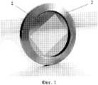
Изобретение поясняется чертежами, где на фиг. 1 представлен общий вид устройства мембранного типа; на фиг. 2 приведено поперечное сечение места крепления мембраны к пластинам. Позициями на чертежах обозначены:The invention is illustrated by drawings, where in FIG. 1 is a perspective view of a membrane type device; in FIG. 2 shows a cross section of the attachment of the membrane to the plates. The positions in the drawings indicate:
1 - мембрана;1 - membrane;
2 - пластина;2 - plate;
3 - углубление;3 - deepening;
4 - припой.4 - solder.
Устройство мембранного типа содержит плоскую или профильную металлическую мембрану 1, на которой может быть выполнена дифракционная, интерференционная или поляризующая сетка или решетка. Мембрана зафиксирована при помощи припоя между двумя металлическими пластинами 2, форма каждой из которых полностью повторяет конфигурацию периметра мембраны, причем внешняя кромка пластин выступает за пределы периметра мембраны. Внутренняя кромка пластин образует отверстие, необходимое для попадания электромагнитного излучения на поверхность мембраны с выполненной на ней дифракционной, интерференционной или поляризующей сеткой или решеткой в процессе работы устройства. Поверхность со стороны мембраны одной из пластин выполнена плоской, а у другой снабжена углублением 3, выполненным таким образом, чтобы граница углубления выходила за пределы периметра мембраны, а глубина углубления превышала толщину мембраны на столько, чтобы при соприкосновении пластин между собой, между мембраной и пластинами мог быть размещен слой припоя 4.The membrane type device comprises a flat or
Для осуществления сборки устройства пластину 2 с углублением 3 располагают углублением вверх, в углубление помещают слой припоя, на припое размещают мембрану 1. Сверху на мембране, а также на поверхности пластины за пределами углубления располагают слой припоя. Нагревают припой до температуры плавления и размещают сверху пластину с плоской поверхностью. Верхняя пластина опускается до соприкосновения с нижней пластиной через тонкий слой припоя, при этом мембрана свободно погружается в расплавленный припой, расположенный в углублении, и не деформируется под давлением верхней пластины. Излишки припоя при необходимости удаляют. После остывания припоя устройство мембранного типа приобретает необходимую прочность и готово к использованию.To assemble the device, a
Claims (1)
Translated fromRussianPriority Applications (1)
| Application Number | Priority Date | Filing Date | Title |
|---|---|---|---|
| RU2012156631/08ARU2561195C2 (en) | 2012-12-26 | 2012-12-26 | Membrane-type device |
Applications Claiming Priority (1)
| Application Number | Priority Date | Filing Date | Title |
|---|---|---|---|
| RU2012156631/08ARU2561195C2 (en) | 2012-12-26 | 2012-12-26 | Membrane-type device |
Publications (2)
| Publication Number | Publication Date |
|---|---|
| RU2012156631A RU2012156631A (en) | 2014-07-10 |
| RU2561195C2true RU2561195C2 (en) | 2015-08-27 |
Family
ID=51215455
Family Applications (1)
| Application Number | Title | Priority Date | Filing Date |
|---|---|---|---|
| RU2012156631/08ARU2561195C2 (en) | 2012-12-26 | 2012-12-26 | Membrane-type device |
Country Status (1)
| Country | Link |
|---|---|
| RU (1) | RU2561195C2 (en) |
Citations (3)
| Publication number | Priority date | Publication date | Assignee | Title |
|---|---|---|---|---|
| RU2231812C2 (en)* | 2002-05-21 | 2004-06-27 | Институт систем обработки изображений РАН | Process of manufacture of diffraction optical elements |
| EP1640325A2 (en)* | 2004-09-27 | 2006-03-29 | Idc, Llc | Method and system for sealing a substrate |
| RU2393512C1 (en)* | 2009-03-05 | 2010-06-27 | Федеральное государственное унитарное предприятие "Научно-производственное предприятие "Исток" (ФГУП НПП "Исток") | Method to produce diffraction grating |
- 2012
- 2012-12-26RURU2012156631/08Apatent/RU2561195C2/ennot_activeIP Right Cessation
Patent Citations (3)
| Publication number | Priority date | Publication date | Assignee | Title |
|---|---|---|---|---|
| RU2231812C2 (en)* | 2002-05-21 | 2004-06-27 | Институт систем обработки изображений РАН | Process of manufacture of diffraction optical elements |
| EP1640325A2 (en)* | 2004-09-27 | 2006-03-29 | Idc, Llc | Method and system for sealing a substrate |
| RU2393512C1 (en)* | 2009-03-05 | 2010-06-27 | Федеральное государственное унитарное предприятие "Научно-производственное предприятие "Исток" (ФГУП НПП "Исток") | Method to produce diffraction grating |
Also Published As
| Publication number | Publication date |
|---|---|
| RU2012156631A (en) | 2014-07-10 |
Similar Documents
| Publication | Publication Date | Title |
|---|---|---|
| ES2637766T3 (en) | Flat arrangement of electronically orientable phase antennas | |
| TWI461783B (en) | Method of fabricating liquid crystal display device | |
| KR101997268B1 (en) | Polarizer edge rib modification | |
| JP6051417B1 (en) | Switch case and switch | |
| RU2014110523A (en) | RFID CHIP MODULE | |
| US20170285284A1 (en) | Opto-electric hybrid board and method of manufacturing same | |
| US20160282526A1 (en) | Curved Grating, Method for Manufacturing the Same, and Optical Device | |
| RU2013106520A (en) | FIXED FIXING METAL INSERT | |
| JP2006066864A5 (en) | ||
| KR102728020B1 (en) | Deposition mask, frame-attached deposition mask, deposition mask preparation body, method for manufacturing deposition mask, method for manufacturing organic semiconductor device, method for manufacturing organic EL display, and method for forming pattern | |
| US10295769B2 (en) | Opto-electric hybrid board and method of manufacturing same | |
| US20110169377A1 (en) | Piezoelectric oscillator | |
| JP2014153586A (en) | Liquid crystal display device | |
| KR101659961B1 (en) | Grid pattern sheet for thin film deposition, manufacturing apparatus of mask assembly, and mask assembly therefrom | |
| RU2561195C2 (en) | Membrane-type device | |
| JP6217381B2 (en) | Lattice bending method | |
| RU126518U1 (en) | MEMBRANE TYPE DEVICE | |
| CN103094713A (en) | K band plane patch lens antenna | |
| US10302830B2 (en) | Wire grid device | |
| CN104090376A (en) | Design method of high-numerical-aperture short-focal-length step phase position type thick FZP | |
| JP6017123B2 (en) | Probe for passing electrical signals, electrical connection device using the same, and probe manufacturing method | |
| JP2011082152A (en) | Ion gun and grid used for it | |
| CN103233206B (en) | Fish-fork-shaped continuous metal film wave-absorbing material and preparation method thereof | |
| WO2016199480A1 (en) | Elastic wave device | |
| JP6940804B2 (en) | Thin-film deposition pattern forming method, thin-film deposition pattern forming device, thin-film deposition mask with frame, and frame |
Legal Events
| Date | Code | Title | Description |
|---|---|---|---|
| MM4A | The patent is invalid due to non-payment of fees | Effective date:20161227 |