RU2469433C1 - Method for laser separation of epitaxial film or layer of epitaxial film from growth substrate of epitaxial semiconductor structure (versions) - Google Patents
Method for laser separation of epitaxial film or layer of epitaxial film from growth substrate of epitaxial semiconductor structure (versions)Download PDFInfo
- Publication number
- RU2469433C1 RU2469433C1RU2011129184/28ARU2011129184ARU2469433C1RU 2469433 C1RU2469433 C1RU 2469433C1RU 2011129184/28 ARU2011129184/28 ARU 2011129184/28ARU 2011129184 ARU2011129184 ARU 2011129184ARU 2469433 C1RU2469433 C1RU 2469433C1
- Authority
- RU
- Russia
- Prior art keywords
- epitaxial
- film
- epitaxial film
- laser
- substrate
- Prior art date
Links
Images


Classifications
- H—ELECTRICITY
- H01—ELECTRIC ELEMENTS
- H01L—SEMICONDUCTOR DEVICES NOT COVERED BY CLASS H10
- H01L21/00—Processes or apparatus adapted for the manufacture or treatment of semiconductor or solid state devices or of parts thereof
- H01L21/67—Apparatus specially adapted for handling semiconductor or electric solid state devices during manufacture or treatment thereof; Apparatus specially adapted for handling wafers during manufacture or treatment of semiconductor or electric solid state devices or components ; Apparatus not specifically provided for elsewhere
- H01L21/683—Apparatus specially adapted for handling semiconductor or electric solid state devices during manufacture or treatment thereof; Apparatus specially adapted for handling wafers during manufacture or treatment of semiconductor or electric solid state devices or components ; Apparatus not specifically provided for elsewhere for supporting or gripping
- H01L21/6835—Apparatus specially adapted for handling semiconductor or electric solid state devices during manufacture or treatment thereof; Apparatus specially adapted for handling wafers during manufacture or treatment of semiconductor or electric solid state devices or components ; Apparatus not specifically provided for elsewhere for supporting or gripping using temporarily an auxiliary support
- H—ELECTRICITY
- H01—ELECTRIC ELEMENTS
- H01L—SEMICONDUCTOR DEVICES NOT COVERED BY CLASS H10
- H01L21/00—Processes or apparatus adapted for the manufacture or treatment of semiconductor or solid state devices or of parts thereof
- H01L21/02—Manufacture or treatment of semiconductor devices or of parts thereof
- H01L21/02104—Forming layers
- H01L21/02365—Forming inorganic semiconducting materials on a substrate
- H01L21/02518—Deposited layers
- H01L21/02521—Materials
- H01L21/02524—Group 14 semiconducting materials
- H01L21/02527—Carbon, e.g. diamond-like carbon
- H—ELECTRICITY
- H01—ELECTRIC ELEMENTS
- H01L—SEMICONDUCTOR DEVICES NOT COVERED BY CLASS H10
- H01L21/00—Processes or apparatus adapted for the manufacture or treatment of semiconductor or solid state devices or of parts thereof
- H01L21/02—Manufacture or treatment of semiconductor devices or of parts thereof
- H01L21/02104—Forming layers
- H01L21/02365—Forming inorganic semiconducting materials on a substrate
- H01L21/02518—Deposited layers
- H01L21/02521—Materials
- H01L21/02524—Group 14 semiconducting materials
- H01L21/02529—Silicon carbide
- H—ELECTRICITY
- H01—ELECTRIC ELEMENTS
- H01L—SEMICONDUCTOR DEVICES NOT COVERED BY CLASS H10
- H01L21/00—Processes or apparatus adapted for the manufacture or treatment of semiconductor or solid state devices or of parts thereof
- H01L21/02—Manufacture or treatment of semiconductor devices or of parts thereof
- H01L21/02104—Forming layers
- H01L21/02365—Forming inorganic semiconducting materials on a substrate
- H01L21/02518—Deposited layers
- H01L21/02521—Materials
- H01L21/02524—Group 14 semiconducting materials
- H01L21/02532—Silicon, silicon germanium, germanium
- H—ELECTRICITY
- H01—ELECTRIC ELEMENTS
- H01L—SEMICONDUCTOR DEVICES NOT COVERED BY CLASS H10
- H01L21/00—Processes or apparatus adapted for the manufacture or treatment of semiconductor or solid state devices or of parts thereof
- H01L21/02—Manufacture or treatment of semiconductor devices or of parts thereof
- H01L21/02104—Forming layers
- H01L21/02365—Forming inorganic semiconducting materials on a substrate
- H01L21/02518—Deposited layers
- H01L21/02521—Materials
- H01L21/02538—Group 13/15 materials
- H01L21/0254—Nitrides
- H—ELECTRICITY
- H01—ELECTRIC ELEMENTS
- H01L—SEMICONDUCTOR DEVICES NOT COVERED BY CLASS H10
- H01L21/00—Processes or apparatus adapted for the manufacture or treatment of semiconductor or solid state devices or of parts thereof
- H01L21/02—Manufacture or treatment of semiconductor devices or of parts thereof
- H01L21/02104—Forming layers
- H01L21/02365—Forming inorganic semiconducting materials on a substrate
- H01L21/02518—Deposited layers
- H01L21/02521—Materials
- H01L21/02538—Group 13/15 materials
- H01L21/02546—Arsenides
- H—ELECTRICITY
- H01—ELECTRIC ELEMENTS
- H01L—SEMICONDUCTOR DEVICES NOT COVERED BY CLASS H10
- H01L21/00—Processes or apparatus adapted for the manufacture or treatment of semiconductor or solid state devices or of parts thereof
- H01L21/02—Manufacture or treatment of semiconductor devices or of parts thereof
- H01L21/02104—Forming layers
- H01L21/02365—Forming inorganic semiconducting materials on a substrate
- H01L21/02518—Deposited layers
- H01L21/02521—Materials
- H01L21/02551—Group 12/16 materials
- H—ELECTRICITY
- H01—ELECTRIC ELEMENTS
- H01L—SEMICONDUCTOR DEVICES NOT COVERED BY CLASS H10
- H01L21/00—Processes or apparatus adapted for the manufacture or treatment of semiconductor or solid state devices or of parts thereof
- H01L21/02—Manufacture or treatment of semiconductor devices or of parts thereof
- H01L21/02104—Forming layers
- H01L21/02365—Forming inorganic semiconducting materials on a substrate
- H01L21/02518—Deposited layers
- H01L21/0257—Doping during depositing
- H—ELECTRICITY
- H01—ELECTRIC ELEMENTS
- H01L—SEMICONDUCTOR DEVICES NOT COVERED BY CLASS H10
- H01L21/00—Processes or apparatus adapted for the manufacture or treatment of semiconductor or solid state devices or of parts thereof
- H01L21/02—Manufacture or treatment of semiconductor devices or of parts thereof
- H01L21/02104—Forming layers
- H01L21/02365—Forming inorganic semiconducting materials on a substrate
- H01L21/02612—Formation types
- H01L21/02617—Deposition types
- H01L21/02634—Homoepitaxy
- H—ELECTRICITY
- H01—ELECTRIC ELEMENTS
- H01L—SEMICONDUCTOR DEVICES NOT COVERED BY CLASS H10
- H01L21/00—Processes or apparatus adapted for the manufacture or treatment of semiconductor or solid state devices or of parts thereof
- H01L21/02—Manufacture or treatment of semiconductor devices or of parts thereof
- H01L21/04—Manufacture or treatment of semiconductor devices or of parts thereof the devices having potential barriers, e.g. a PN junction, depletion layer or carrier concentration layer
- H01L21/18—Manufacture or treatment of semiconductor devices or of parts thereof the devices having potential barriers, e.g. a PN junction, depletion layer or carrier concentration layer the devices having semiconductor bodies comprising elements of Group IV of the Periodic Table or AIIIBV compounds with or without impurities, e.g. doping materials
- H01L21/26—Bombardment with radiation
- H01L21/263—Bombardment with radiation with high-energy radiation
- H01L21/268—Bombardment with radiation with high-energy radiation using electromagnetic radiation, e.g. laser radiation
- H—ELECTRICITY
- H01—ELECTRIC ELEMENTS
- H01L—SEMICONDUCTOR DEVICES NOT COVERED BY CLASS H10
- H01L21/00—Processes or apparatus adapted for the manufacture or treatment of semiconductor or solid state devices or of parts thereof
- H01L21/70—Manufacture or treatment of devices consisting of a plurality of solid state components formed in or on a common substrate or of parts thereof; Manufacture of integrated circuit devices or of parts thereof
- H01L21/71—Manufacture of specific parts of devices defined in group H01L21/70
- H01L21/76—Making of isolation regions between components
- H01L21/762—Dielectric regions, e.g. EPIC dielectric isolation, LOCOS; Trench refilling techniques, SOI technology, use of channel stoppers
- H01L21/7624—Dielectric regions, e.g. EPIC dielectric isolation, LOCOS; Trench refilling techniques, SOI technology, use of channel stoppers using semiconductor on insulator [SOI] technology
- H01L21/76251—Dielectric regions, e.g. EPIC dielectric isolation, LOCOS; Trench refilling techniques, SOI technology, use of channel stoppers using semiconductor on insulator [SOI] technology using bonding techniques
- H01L21/76254—Dielectric regions, e.g. EPIC dielectric isolation, LOCOS; Trench refilling techniques, SOI technology, use of channel stoppers using semiconductor on insulator [SOI] technology using bonding techniques with separation/delamination along an ion implanted layer, e.g. Smart-cut, Unibond
- H—ELECTRICITY
- H01—ELECTRIC ELEMENTS
- H01L—SEMICONDUCTOR DEVICES NOT COVERED BY CLASS H10
- H01L2221/00—Processes or apparatus adapted for the manufacture or treatment of semiconductor or solid state devices or of parts thereof covered by H01L21/00
- H01L2221/67—Apparatus for handling semiconductor or electric solid state devices during manufacture or treatment thereof; Apparatus for handling wafers during manufacture or treatment of semiconductor or electric solid state devices or components; Apparatus not specifically provided for elsewhere
- H01L2221/683—Apparatus for handling semiconductor or electric solid state devices during manufacture or treatment thereof; Apparatus for handling wafers during manufacture or treatment of semiconductor or electric solid state devices or components; Apparatus not specifically provided for elsewhere for supporting or gripping
- H01L2221/68304—Apparatus for handling semiconductor or electric solid state devices during manufacture or treatment thereof; Apparatus for handling wafers during manufacture or treatment of semiconductor or electric solid state devices or components; Apparatus not specifically provided for elsewhere for supporting or gripping using temporarily an auxiliary support
- H01L2221/68381—Details of chemical or physical process used for separating the auxiliary support from a device or wafer
- H—ELECTRICITY
- H10—SEMICONDUCTOR DEVICES; ELECTRIC SOLID-STATE DEVICES NOT OTHERWISE PROVIDED FOR
- H10H—INORGANIC LIGHT-EMITTING SEMICONDUCTOR DEVICES HAVING POTENTIAL BARRIERS
- H10H20/00—Individual inorganic light-emitting semiconductor devices having potential barriers, e.g. light-emitting diodes [LED]
- H10H20/01—Manufacture or treatment
- H10H20/011—Manufacture or treatment of bodies, e.g. forming semiconductor layers
- H10H20/018—Bonding of wafers
Landscapes
- Engineering & Computer Science (AREA)
- Physics & Mathematics (AREA)
- Condensed Matter Physics & Semiconductors (AREA)
- General Physics & Mathematics (AREA)
- Manufacturing & Machinery (AREA)
- Computer Hardware Design (AREA)
- Microelectronics & Electronic Packaging (AREA)
- Power Engineering (AREA)
- High Energy & Nuclear Physics (AREA)
- Electromagnetism (AREA)
- Optics & Photonics (AREA)
- Health & Medical Sciences (AREA)
- Toxicology (AREA)
- Recrystallisation Techniques (AREA)
- Crystals, And After-Treatments Of Crystals (AREA)
- Laser Beam Processing (AREA)
Abstract
Description
Translated fromRussianОБЛАСТЬ ТЕХНИКИ, К КОТОРОЙ ОТНОСИТСЯ ИЗОБРЕТЕНИЕFIELD OF THE INVENTION
Группа изобретений относится к области лазерной обработки твердых материалов, в частности к способу отделения поверхностных слоев полупроводниковых кристаллов с помощью лазерного излучения, а именно к лазерному отделению эпитаксиальной пленки или слоя эпитаксиальной пленки от ростовой подложки эпитаксиальной полупроводниковой структуры.The group of inventions relates to the field of laser processing of solid materials, in particular to a method for separating surface layers of semiconductor crystals using laser radiation, namely, laser separation of an epitaxial film or layer of an epitaxial film from a growth substrate of an epitaxial semiconductor structure.
УРОВЕНЬ ТЕХНИКИBACKGROUND
Лазерное отделение эпитаксиальных слоев полупроводниковых кристаллов от ростовых подложек с переносом их на неростовые подложки широко применяется в настоящее время при изготовлении светодиодов (патенты US 7241667, US 7202141) и лазерных диодов (US 6365429) по технологии флип-чип.Laser separation of epitaxial layers of semiconductor crystals from growth substrates with their transfer to non-growth substrates is widely used at present in the manufacture of LEDs (patents US 7241667, US 7202141) and laser diodes (US 6365429) using flip chip technology.
Впервые лазерное отделение слоев нитрида галлия от прозрачных ростовых подложек сапфира было предложено в работе Kelly et al Physica Status Solidi(a) vol. 159, pp.R3, R4, (1997). В этой работе использовался ультрафиолетовый эксимерный лазер с длиной волны λ=355 нм, удовлетворяющей соотношению 2пħc/Eg1<λ<2пħc/Eg2, для которой энергия кванта находится внутри запрещенной зоны подложки Eg1, сделанной из сапфира, но превышает ширину запрещенной зоны эпитаксиальной пленки Eg2, состоящей из нитрида галлия.Laser separation of gallium nitride layers from transparent growth sapphire substrates was first proposed by Kelly et al Physica Status Solidi (a) vol. 159, pp. R3, R4, (1997). In this work, we used an ultraviolet excimer laser with a wavelength of λ = 355 nm, satisfying the ratio 2пħc / Eg1 <λ <2пħc / Eg2 , for which the quantum energy is inside the band gap of the substrate Eg1 made of sapphire, but exceeds the band gap epitaxial film Eg2 consisting of gallium nitride.
Впоследствии способ лазерного отделения, основанный на различии ширин запрещенных зон ростовой подложки и эпитаксиальной пленки, был усовершенствован. В частности, для улучшения качества отделенной эпитаксиальной пленки и подавления ее растрескивания было предложено использовать добавочный жертвенный слой с шириной запрещенной зоны, меньшей ширины запрещенных зон ростовой подложки и эпитаксиальной пленки, а также применять сканирование лазерным лучом гетероэпитаксиальной границы раздела между ростовой подложкой и эпитаксиальной пленкой (патенты US 6071795, US 6365429).Subsequently, the laser separation method based on the difference between the bandgaps of the growth substrate and the epitaxial film was improved. In particular, to improve the quality of the separated epitaxial film and suppress its cracking, it was proposed to use an additional sacrificial layer with a band gap smaller than the band gap of the growth substrate and the epitaxial film, and also use a laser beam scan of the heteroepitaxial interface between the growth substrate and the epitaxial film ( patents US 6071795, US 6365429).
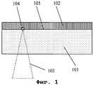
Общая схема способов лазерного отделения, основанных на различии ширин запрещенных зон ростовой подложки и эпитаксиальной пленки, показана на Фиг.1.The general scheme of laser separation methods based on the difference between the bandgaps of the growth substrate and the epitaxial film is shown in FIG.
При облучении ультрафиолетовым светом со стороны подложки гетероэпитаксиальной полупроводниковой пленки 102 нитрида галлия, выращенной на подложке 101 из сапфира, имеющего ширину запрещенной зоны, большую, чем энергия кванта света, ультрафиолетовое лазерное излучение проходит сквозь сапфир и поглощается в тонком слое нитрида галлия вблизи гетероэпитаксиальной границы раздела 105 нитрид галлия - сапфир. Под воздействием ультрафиолетового лазерного излучения, нитрид галлия в области 104, определяемой пересечением ультрафиолетового лазерного луча 103 с гетероэпитаксиальной границей раздела 105, нагревается до температуры T1, превышающей температуру разложения T0~900°C, и разлагается на газообразный азот и жидкий галлий, и в результате эпитаксиальная пленка нитрида галлия отделяется от сапфира.When irradiated with ultraviolet light from the substrate side of a
Все предложенные ранее способы лазерного отделения эпитаксиальных пленок от ростовых подложек основаны на различии ширин запрещенных зон эпитаксиальной пленки Eg2 и подложки Eg1. Эти способы могут успешно применяться для отделения эпитаксиальных пленок, полученных с использованием метода гетероэпитаксии, т.е. технологии наращивания эпитаксиальной пленки на ростовой подложке, выполненной из материала, отличного от материала эпитаксиальной пленки.All previously proposed methods for laser separation of epitaxial films from growth substrates are based on the difference between the bandgaps of the epitaxial film Eg2 and the substrate Eg1 . These methods can be successfully used to separate epitaxial films obtained using the heteroepitaxy method, i.e. technologies for growing an epitaxial film on a growth substrate made of a material different from the material of the epitaxial film.
Однако для получения высококачественных эпитаксиальных пленок, без встроенных механических напряжений, часто бывает необходимо использовать метод гомоэпитаксии, который предполагает наращивание эпитаксиальной пленки на ростовой подложке из того же самого материала, что и эпитаксиальная пленка. В этом случае ростовая подложка и эпитаксиальная пленка имеют одинаковую ширину запрещенной зоны, и обычный метод лазерного отделения, описанный выше, становится неприменимым.However, to obtain high-quality epitaxial films without built-in mechanical stresses, it is often necessary to use the homoepitaxy method, which involves building up an epitaxial film on a growth substrate of the same material as the epitaxial film. In this case, the growth substrate and the epitaxial film have the same band gap, and the usual laser separation method described above becomes inapplicable.
Задачей настоящего изобретения является расширение области применения способа, а именно обеспечение возможности отделять эпитаксиальные пленки от подложек, выполненных из того же самого кристаллического материала, что и эпитаксиальная пленка.The objective of the present invention is to expand the scope of the method, namely, providing the ability to separate epitaxial films from substrates made of the same crystalline material as the epitaxial film.
РАСКРЫТИЕ ИЗОБРЕТЕНИЯSUMMARY OF THE INVENTION
Для решения этой задачи предлагается два варианта способа лазерного отделения эпитаксиальной пленки или слоя эпитаксиальной пленки от ростовой подложки эпитаксиальной полупроводниковой структуры.To solve this problem, two variants of a method for laser separation of an epitaxial film or layer of an epitaxial film from a growth substrate of an epitaxial semiconductor structure are proposed.
В первом варианте способа при выращивании эпитаксиальной пленки или слоя эпитаксиальной пленки используют селективное легирование мелкими донорными или акцепторными примесями некоторых областей эпитаксиальной структуры, так что результирующая концентрация мелких примесей в селективно легированных областях существенно превосходит фоновую концентрацию в нелегированных областях. Затем направляют сфокусированный лазерный луч на эпитаксиальную структуру, состоящую из подложки и эпитаксиальной пленки, так, что фокус луча расположен в селективно легированных областях кристаллической структуры, в которых происходит поглощение лазерного излучения. Лазерный луч перемещают с осуществлением сканирования фокусом луча селективно легированных областей эпитаксиальной структуры с частичным термическим разложением селективно легированных областей и уменьшением их механической прочности. После лазерного сканирования эпитаксиальную структуру наклеивают на временную подложку и отделяют эпитаксиальную пленку или слой эпитаксиальной пленки от ростовой подложки или ростовой подложки с частью эпитаксиальной пленки посредством приложения механического или термомеханического напряжения.In the first variant of the method, when growing an epitaxial film or layer of an epitaxial film, selective doping with small donor or acceptor impurities of certain regions of the epitaxial structure is used, so that the resulting concentration of small impurities in selectively doped regions significantly exceeds the background concentration in undoped regions. The focused laser beam is then directed to an epitaxial structure consisting of a substrate and an epitaxial film, so that the beam focus is located in selectively doped regions of the crystal structure in which laser radiation is absorbed. The laser beam is moved by scanning with the beam focus of selectively doped regions of the epitaxial structure with partial thermal decomposition of the selectively doped regions and a decrease in their mechanical strength. After laser scanning, the epitaxial structure is glued onto a temporary substrate and the epitaxial film or layer of the epitaxial film is separated from the growth substrate or growth substrate with a part of the epitaxial film by applying mechanical or thermomechanical stress.
Второй вариант способа характеризуется теми же признаками, а отличается от первого тем, что эпитаксиальную структуру наклеивают на временную подложку перед лазерным сканированием, затем проводят лазерное сканирование эпитаксиальной структуры, наклеенной на временную подложку, и после лазерного сканирования отделяют эпитаксиальную пленку или слой эпитаксиальной пленки от ростовой подложки или ростовой подложки с частью эпитаксиальной пленки посредством приложения механического или термомеханического напряжения.The second variant of the method is characterized by the same features, but differs from the first in that the epitaxial structure is glued to a temporary substrate before laser scanning, then the laser scanning of the epitaxial structure glued to the temporary substrate is carried out, and after laser scanning the epitaxial film or layer of the epitaxial film is separated from the growth substrate or growth substrate with a part of the epitaxial film by applying mechanical or thermomechanical stress.
Предпочтительно, эпитаксиальная пленка или слой эпитаксиальной пленки выращена методом гомоэпитаксии.Preferably, the epitaxial film or layer of the epitaxial film is grown by homoepitaxy.
Предпочтительно, селективно легированной областью является подложка или поверхностный слой подложки.Preferably, the selectively doped region is a substrate or a surface layer of a substrate.
Предпочтительно, селективно легированной областью является эпитаксиальная пленка или нижний слой эпитаксиальной пленки.Preferably, the selectively doped region is an epitaxial film or a lower layer of an epitaxial film.
Предпочтительно, материалом кристаллической структуры, состоящей из подложки и эпитаксиальной пленки, является полупроводник из элементов четвертой группы, или полупроводниковое соединение из элементов четвертой группы, или полупроводниковое соединение из элементов третьей и пятой групп, или полупроводниковое соединение из элементов второй и шестой групп периодической таблицы элементов.Preferably, the material of the crystal structure consisting of the substrate and the epitaxial film is a semiconductor of the elements of the fourth group, or a semiconductor compound of the elements of the fourth group, or a semiconductor compound of the elements of the third and fifth groups, or a semiconductor compound of the elements of the second and sixth groups of the periodic table of elements .
Предпочтительно, длина волны лазера для отделения гомоэпитаксиальных пленок от ростовой подложки лежит в следующих диапазонах длин волн: для полупроводников кремния, германия и арсенида галлия в диапазоне 6 мкм ≤ λ ≤ 48 мкм, для нитрида галлия в диапазоне 4 мкм ≤ λ ≤ 32 мкм, для карбида кремния 3 мкм ≤ λ ≤ 24 мкм, для нитрида алюминия в диапазоне 2,5 мкм ≤ λ ≤ 20 мкм, и для алмаза - 2 мкм ≤ λ ≤ 16 мкм.Preferably, the laser wavelength for separating homoepitaxial films from the growth substrate lies in the following wavelength ranges: for silicon, germanium and gallium arsenide semiconductors in the range of 6 μm ≤ λ ≤ 48 μm, for gallium nitride in the range of 4 μm ≤ λ ≤ 32 μm, for silicon carbide 3 μm ≤ λ ≤ 24 μm, for aluminum nitride in the range 2.5 μm ≤ λ ≤ 20 μm, and for diamond - 2 μm ≤ λ ≤ 16 μm.
Предпочтительно, в качестве лазера используется инфракрасный газовый лазер с импульсной накачкой на двуокиси углерода CO2 или монооксиде углерода CO.Preferably, a pulsed-pumped infrared gas laser using carbon dioxide CO2 or carbon monoxide CO is used as the laser.
Предложенные варианты способа лазерного отделения позволяют отделять гомоэпитаксиальные пленки от подложек, выполненных из того же самого кристаллического материала, что и эпитаксиальная пленка. Этот новый способ лазерного отделения основан на использовании селективного легирования подложки и эпитаксиальной пленки мелкими донорными или акцепторными примесями. При селективном легировании концентрации свободных носителей в эпитаксиальной пленке и подложке могут существенно отличаться, и это может приводить к сильному отличию коэффициентов поглощения света в инфракрасной области вблизи области остаточных лучей, где существенны вклады в инфракрасное поглощение оптических фононов, свободных носителей и фонон-плазмонного взаимодействия оптических фононов со свободными носителями.The proposed variants of the laser separation method make it possible to separate homoepitaxial films from substrates made of the same crystalline material as the epitaxial film. This new laser separation method is based on the use of selective doping of the substrate and epitaxial film with small donor or acceptor impurities. With selective doping, the concentrations of free carriers in the epitaxial film and the substrate can differ significantly, and this can lead to a strong difference in the absorption coefficients of light in the infrared region near the region of residual rays, where contributions to the infrared absorption of optical phonons, free carriers, and phonon-plasmon interaction between optical phonons with free carriers.
Соответствующим подбором уровней легирования и частоты инфракрасного лазерного излучения можно добиться того, чтобы лазерное излучение поглощалось в основном в области сильного легирования вблизи границы раздела подложка - гомоэпитаксиальная пленка. При сканировании границы раздела подложка - гомоэпитаксиальная пленка сфокусированным лазерным лучем достаточной мощности происходит термическое разложение полупроводникового кристалла с последующим отделением гомоэпитаксиальной пленки.By appropriate selection of the doping levels and the frequency of infrared laser radiation, it is possible to ensure that laser radiation is absorbed mainly in the region of strong doping near the interface between the substrate and the homoepitaxial film. When scanning the substrate – homoepitaxial film interface with a focused laser beam of sufficient power, the semiconductor crystal undergoes thermal decomposition followed by separation of the homoepitaxial film.
Для осуществления предложенного способа лазерного отделения предпочтительно использовать лазерное излучение с длиной волны λ, лежащей в инфракрасной области относительной прозрачности нелегированного полупроводника, а именно вблизи края области остаточных лучей, где невозможно сильное поглощение света за счет одно- и двухфононных процессов, но может присутствовать относительно слабое поглощение за счет трех- и более фононных процессов.To implement the proposed method of laser separation, it is preferable to use laser radiation with a wavelength λ lying in the infrared region of the relative transparency of the undoped semiconductor, namely, near the edge of the region of residual rays, where strong absorption of light due to one- and two-phonon processes is impossible, but relatively weak may be present absorption due to three or more phonon processes.
Предпочтительно, длина волны λ лазерного луча заключена в интервале c/4ν0≤λ≤2c/ν0, где ν0 - частота LO-оптического фонона для полупроводникового материала ростовой подложки, c - скорость света.Preferably, the wavelength λ of the laser beam is in the range c / 4ν0 ≤λ ≤ 2c / ν0 , where ν0 is the frequency of the LO optical phonon for the semiconductor material of the growth substrate, c is the speed of light.
Из приведенного выше неравенства следует, что предпочтительная длина волны лазера для отделения гомоэпитаксиальных пленок от ростовой подложки лежит в следующих диапазонах длин волн: для полупроводников кремния, германия и арсенида галлия в диапазоне 6 мкм ≤ λ ≤ 48 мкм, для нитрида галлия в диапазоне 4 мкм ≤ λ ≤ 32 мкм, для карбида кремния - 3 мкм ≤ λ ≤ 24 мкм, для нитрида алюминия в диапазоне 2,5 мкм ≤ λ ≤ 20 мкм, и для алмаза - 2 мкм ≤ λ ≤ 16 мкм.From the above inequality it follows that the preferred laser wavelength for separating homoepitaxial films from the growth substrate lies in the following wavelength ranges: for silicon, germanium and gallium arsenide semiconductors in the range of 6 μm ≤ λ ≤ 48 μm, for gallium nitride in the range of 4 μm ≤ λ ≤ 32 μm, for silicon carbide - 3 μm ≤ λ ≤ 24 μm, for aluminum nitride in the range of 2.5 μm ≤ λ ≤ 20 μm, and for diamond - 2 μm ≤ λ ≤ 16 μm.
Технический результат предложенного изобретения состоит в предложении нового по сравнению с ранее известными способа лазерного отделения эпитаксиальных пленок, который позволяет отделять от подложек гомоэпитаксиальные пленки, т.е. эпитаксиальные пленки, имеющие ту же ширину запрещенной зоны, что и исходная полупроводниковая подложка. Также предложенный способ позволяет использовать для отделения эпитаксиальных пленок высокоэффективные и недорогие инфракрасные газовые лазеры на двуокиси углерода CO2 или монооксиде углерода СО.The technical result of the proposed invention consists in proposing a new method for laser separation of epitaxial films, which allows separating homoepitaxial films from substrates, i.e. epitaxial films having the same band gap as the original semiconductor substrate. Also, the proposed method allows the use of highly efficient and inexpensive infrared gas lasers based on carbon dioxide CO2 or carbon monoxide CO to separate epitaxial films.
КРАТКОЕ ОПИСАНИЕ ЧЕРТЕЖЕЙBRIEF DESCRIPTION OF THE DRAWINGS
Настоящее изобретение иллюстрируется чертежами, на которых представлен известный уровень техники, Фиг.1, схемы, иллюстрирующие реализацию настоящего изобретения, Фиг.2-5, и расчетные спектральные зависимости коэффициента поглощения света в нитриде галлия при различных уровнях легирования мелкими донорными примесями, Фиг.6.The present invention is illustrated by drawings, which show the prior art, FIG. 1, diagrams illustrating the implementation of the present invention, FIGS. 2-5, and calculated spectral dependences of the light absorption coefficient in gallium nitride at various levels of doping with small donor impurities, FIG. 6 .
На Фиг.1 представлена схема известного из уровня техники способа лазерного отделения гетероэпитаксиальной пленки полупроводникового кристалла от инородной ростовой подложки с использованием сфокусированного лазерного излучения, с длиной волны λ, для которой энергия кванта света находится внутри запрещенной зоны подложки Eg1 и превышает ширину запрещенной зоны материала эпитаксиальной пленки Eg2.Figure 1 presents a diagram of a prior art method for laser separation of a heteroepitaxial film of a semiconductor crystal from a foreign growth substrate using focused laser radiation with a wavelength λ for which the light quantum energy is inside the band gap of the substrate Eg1 and exceeds the band gap of the material epitaxial film Eg2 .
На Фиг.2 представлена схема, иллюстрирующая предложенный способ лазерного отделения гомоэпитаксиальной пленки от полупроводниковой подложки, состоящей из того же самого полупроводникового материала, что и гомоэпитаксиальная пленка. Схема иллюстрирует лазерное отделение для случая селективного легирования подложки и гомоэпитаксиальной пленки мелкими донорными или акцепторными примесями, когда уровень легирования в гомоэпитаксиальной пленке превышает уровень легирования в полупроводниковой подложке.Figure 2 presents a diagram illustrating the proposed method for laser separation of a homoepitaxial film from a semiconductor substrate consisting of the same semiconductor material as the homoepitaxial film. The scheme illustrates the laser separation for the case of selective doping of the substrate and the homoepitaxial film with small donor or acceptor impurities, when the level of doping in the homoepitaxial film exceeds the level of doping in the semiconductor substrate.
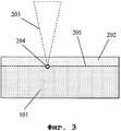
На Фиг.3 представлена схема, иллюстрирующая предложенный способ лазерного отделения гомоэпитаксиальной пленки от полупроводниковой подложки, состоящей из того же самого полупроводникового материала, что и гомоэпитаксиальная пленка. Схема иллюстрирует лазерное отделение для случая селективного легирования подложки и гомоэпитаксиальной пленки мелкими донорными или акцепторными примесями, когда уровень легирования в полупроводниковой подложке превышает уровень легирования в гомоэпитаксиальной пленке.Figure 3 presents a diagram illustrating the proposed method for laser separation of a homoepitaxial film from a semiconductor substrate consisting of the same semiconductor material as the homoepitaxial film. The scheme illustrates the laser separation for the case of selective doping of the substrate and the homoepitaxial film with small donor or acceptor impurities, when the doping level in the semiconductor substrate exceeds the doping level in the homoepitaxial film.
На Фиг.4 представлена схема, иллюстрирующая предложенный способ лазерного отделения нелегированного верхнего слоя гомоэпитаксиальной пленки от нелегированной полупроводниковой подложки с помощью лазерного луча, проходящего сквозь подложку и поглощающегося в нижнем слое гомоэпитаксиальной пленки, легированном мелкими донорными или акцепторными примесями.Figure 4 is a diagram illustrating the proposed method for laser separation of an undoped top layer of a homoepitaxial film from an undoped semiconductor substrate using a laser beam passing through the substrate and absorbed in the lower layer of the homoepitaxial film doped with small donor or acceptor impurities.
На Фиг.5 представлена схема, иллюстрирующая предложенный способ лазерного отделения нелегированного верхнего слоя гомоэпитаксиальной пленки от нелегированной полупроводниковой подложки с помощью лазерного луча, проходящего сквозь верхний нелегированный слой и поглощающегося в нижнем слое гомоэпитаксиальной пленки, легированном мелкими донорными или акцепторными примесями.Figure 5 presents a diagram illustrating the proposed method for laser separation of the undoped top layer of the homoepitaxial film from the undoped semiconductor substrate using a laser beam passing through the upper undoped layer and absorbed in the lower layer of the homoepitaxial film doped with small donor or acceptor impurities.
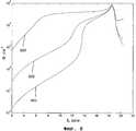
На Фиг.6 представлены рассчитанные спектральные зависимости коэффициента поглощения света вблизи области остаточных лучей для полупроводникового кристалла нитрида галлия при различных уровнях легирования мелкими донорными примесями. Зависимости 601, 602 и 603 относятся к уровням легирования 1017, 1018 и 5·1019 см-3 соответственно.Figure 6 presents the calculated spectral dependences of the light absorption coefficient near the region of residual rays for a gallium nitride semiconductor crystal at various levels of doping with small donor impurities.
ОСУЩЕСТВЛЕНИЕ ИЗОБРЕТЕНИЯDETAILED DESCRIPTION OF THE INVENTION
Настоящее изобретение будет прояснено ниже на нескольких примерах его осуществления. Следует отметить, что последующее описание этих примеров осуществления является лишь иллюстративным и не является исчерпывающим.The present invention will be clarified below with a few examples of its implementation. It should be noted that the following description of these embodiments is merely illustrative and not exhaustive.
Пример 1. Отделение гомоэпитаксиальной пленки нитрида галлия, легированной мелкими донорными примесями, от нелегированной полупроводниковой подложки нитрида галлия с помощью лазерного луча, проходящего сквозь подложку.Example 1. The separation of the homoepitaxial film of gallium nitride doped with small donor impurities from the undoped semiconductor substrate of gallium nitride using a laser beam passing through the substrate.
На Фиг.2 представлена схема лазерного отделения гомоэпитаксиальной пленки 202 нитрида галлия, толщиной 50 мкм от полупроводниковой подложки 101 нитрида галлия, толщиной 200 мкм. Уровень легирования мелкими донорными примесями кремния в гомоэпитаксиальной пленке 202 составляет 5·1019 см-3 и превышает фоновую концентрацию мелких доноров кислорода и кремния в полупроводниковой подложке 101, равный 1017 см-3.Figure 2 presents a diagram of the laser separation of the
Для отделения гомоэпитаксиальной пленки нитрида галлия используется CO2 лазер, работающий в режиме импульсной накачки на длине волны λ=10,6 мкм и генерирующий импульсы с энергией 0,1 Дж, длительностью 50 нс и частотой повторения 100 герц.To separate the homoepitaxial gallium nitride film, a CO2 laser is used, operating in the pulsed pump mode at a wavelength of λ = 10.6 μm and generating pulses with an energy of 0.1 J, a duration of 50 ns, and a repetition rate of 100 hertz.
Коэффициент поглощения лазерного излучения с длиной волны λ=10 мкм в гомоэпитаксиальной пленке 202 нитрида галлия, легированной мелкими донорными примесями кремния с концентрацией 5·1019 см-3, равен 4·104 с-1, тогда как коэффициент поглощения этого излучения в нелегированной полупроводниковой подложке 101 нитрида галлия, с фоновой концентрацией мелких доноров кислорода и кремния, равной 1017 см-3, составляет 5·1019 см-1.The absorption coefficient of laser radiation with a wavelength of λ = 10 μm in a homoepitaxial film of 202 gallium nitride doped with small donor impurities of silicon with a concentration of 5 · 1019 cm-3 is 4 · 104 s-1 , while the absorption coefficient of this radiation in undoped a
Соответствующие спектральные зависимости коэффициента поглощения света вблизи области остаточных лучей, рассчитанные нами для полупроводниковых кристаллов нитрида галлия с различными уровнями легирования мелкими донорными примесями, приведены на Фиг.6. Кривые 601, 602 и 603 относятся к уровням легирования 1017, 1018 и 5·1019 см-3 соответственно.The corresponding spectral dependences of the light absorption coefficient near the region of residual rays, calculated by us for semiconductor crystals of gallium nitride with different levels of doping with small donor impurities, are shown in Fig.6.
Как видно из схемы на Фиг.2, инфракрасный лазерный луч 203 проходит сквозь подложку 101 и фокусируется в пятно диаметром 1 мм, что обеспечивает плотность энергии 10 Дж/см2. Под действием сфокусированного в пятно диаметром 1 мм инфракрасного лазерного луча 203, импульсного CO2 лазера с длиной волны λ=10 мкм, слабо поглощающегося в нелегированной полупроводниковой подложке 101 нитрида галлия и сильно поглощающегося в легированной мелкими донорными примесями гомоэпитаксиальной пленке 202 нитрида галлия, происходит локальный нагрев гомоэпитаксиальной пленки 202 в области 204, определяемой пересечением инфракрасного лазерного луча 203 с гомоэпитаксиальной границей раздела 205 между нелегированной полупроводниковой подложкой 101 и легированной гомоэпитаксиальной пленкой 202. Локальный нагрев до температуры выше 900°C приводит к химическому разложению кристалла нитрида галлия на газообразный азот и жидкий галлий в области 204. Перемещение фокуса лазерного луча 203 со скоростью 10 см/с в горизонтальной плоскости, параллельной гомоэпитаксиальной границе раздела 205, приводит к последовательному разложению нитрида галлия в наборе областей 204 и ослаблению гомоэпитаксиальной границы раздела 205 между нелегированной полупроводниковой подложкой 101 и легированной гомоэпитаксиальной пленкой 202. Наклеивая затем гомоэпитаксиальную пленку 202 на временную металлическую, керамическую или пластиковую подложку и прилагая небольшое механическое или термомеханическое напряжение, можно отделить эпитаксиальную пленку 202 от подложки 101.As can be seen from the diagram in figure 2, the
Пример 2. Отделение нелегированной гомоэпитаксиальной пленки нитрида галлия от легированной мелкими донорными примесями полупроводниковой подложки нитрида галлия с помощью лазерного луча, проходящего сквозь гомоэпитаксиальную пленку.Example 2. The separation of undoped homoepitaxial film of gallium nitride from doped with small donor impurities of the semiconductor substrate of gallium nitride using a laser beam passing through the homoepitaxial film.
На Фиг.3 представлена схема лазерного отделения нелегированной гомоэпитаксиальной пленки 202 нитрида галлия, толщиной 100 мкм, от полупроводниковой подложки 101 нитрида галлия, толщиной 1 мм. Фоновая концентрация мелких доноров кислорода и кремния в гомоэпитаксиальной пленке 202 составляет 1017 см-3 и существенно меньше концентрации мелких донорных примесей кремния в легированной полупроводниковой подложке 101, равной 5·1019 см-3.Figure 3 presents a diagram of the laser separation of the undoped
Для отделения гомоэпитаксиальной пленки нитрида галлия используется CO2 лазер, работающий в режиме импульсной накачки на длине волны λ=10,6 мкм и генерирующий импульсы с энергией 0,1 Дж, длительностью 50 нс и частотой повторения 100 герц. Коэффициент поглощения лазерного излучения с длиной волны λ=10 мкм в нелегированной гомоэпитаксиальной пленке 202 нитрида галлия, с фоновой концентрацией мелких доноров кислорода и кремния, равной 1017 см-3, составляет 5·101 см-1, тогда как коэффициент поглощения этого излучения в полупроводниковой подложке 101 нитрида галлия, легированной мелкими донорными примесями кремния с концентрацией 5·1019 см-3, равен 4·104 см-1. Соответствующие спектральные зависимости коэффициента поглощения света вблизи области остаточных лучей, рассчитанные нами для полупроводниковых кристаллов нитрида галлия с различными уровнями легирования мелкими донорными примесями, приведены на Фиг.6. Кривые 601, 602 и 603 относятся к уровням легирования 1017, 1018 и 5·1019 см-3 соответственно.To separate the homoepitaxial gallium nitride film, a CO2 laser is used, operating in the pulsed pump mode at a wavelength of λ = 10.6 μm and generating pulses with an energy of 0.1 J, a duration of 50 ns, and a repetition rate of 100 hertz. The absorption coefficient of laser radiation with a wavelength of λ = 10 μm in an undoped homoepitaxial film of 202 gallium nitride, with a background concentration of small oxygen and silicon donors equal to 1017 cm-3, is 5 · 101 cm-1 , while the absorption coefficient of this radiation in a
Как видно из схемы на Фиг.3, инфракрасный лазерный луч 203 проходит сквозь гомоэпитаксиальную пленку 202 и фокусируется в пятно диаметром 1 мм, что обеспечивает плотность энергии 10 Дж/см2.As can be seen from the diagram in Figure 3, the
Под действием сфокусированного в пятно диаметром 1 мм инфракрасного лазерного луча 203, импульсного CO2 лазера с длиной волны λ=10,6 мкм, слабо поглощающегося в нелегированной гомоэпитаксиальной пленке 202 нитрида галлия и сильно поглощающегося в легированной мелкими донорными примесями полупроводниковой подложке 101 нитрида галлия, происходит локальный нагрев подложки 101 в области 204, определяемой пересечением инфракрасного лазерного луча 203 с гомоэпитаксиальной границей раздела 205 раздела между легированной полупроводниковой подложкой 101 и нелегированной гомоэпитаксиальной пленкой 202. Локальный нагрев до температуры выше 900°C приводит к химическому разложению кристалла нитрида галлия на газообразный азот и жидкий галлий в области 204. Перемещение фокуса лазерного луча 203 со скоростью 10 см/с в горизонтальной плоскости, параллельной гомоэпитаксиальной границе раздела 205, приводит к последовательному разложению нитрида галлия в наборе областей 204 и ослаблению гомоэпитаксиальной границы раздела 205 между легированной полупроводниковой подложкой 101 и нелегированной гомоэпитаксиальной пленкой 202. Наклеивая затем гомоэпитаксиальную пленку 202 на временную металлическую, керамическую или пластиковую подложку и прилагая небольшое механическое или термомеханическое напряжение, можно отделить гомоэпитаксиальную пленку 202 от подложки 101.Under the influence of an
Пример 3. Отделение нелегированного верхнего слоя гомоэпитаксиальной пленки нитрида галлия от нелегированной полупроводниковой подложки нитрида галлия с помощью лазерного луча, проходящего сквозь подложку и поглощающегося в нижнем слое гомоэпитаксиальной пленки, легированном мелкими донорными примесями. На Фиг.4 представлена схема лазерного отделения нелегированной гомоэпитаксиальной пленки 202 нитрида галлия, толщиной 50 мкм, от нелегированной полупроводниковой подложки 101 нитрида галлия, толщиной 200 мкм, с использованием легированного нижнего слоя 406 омоэпитаксиальной пленки, толщиной 1 мкм. Уровень легирования мелкими донорными примесями кремния в нижнем слое 406 гомоэпитаксиальной пленки нитрида галлия составляет 5·1019 см-3 и превышает фоновую концентрацию мелких доноров кислорода и кремния в полупроводниковой подложке 101, и верхнем слое гомоэпитаксиальной пленки 202, равный 1017 см-3.Example 3. The separation of the undoped top layer of the homoepitaxial gallium nitride film from the undoped semiconductor substrate of gallium nitride using a laser beam passing through the substrate and absorbed in the lower layer of the homoepitaxial film doped with small donor impurities. Figure 4 presents a diagram of a laser separation of an undoped
Для отделения гомоэпитаксиальной пленки нитрида галлия используется CO2 лазер, работающий в режиме импульсной накачки на длине волны λ=10,6 мкм и генерирующий импульсы с энергией 0,1 Дж, длительностью 50 нс и частотой повторения 100 герц.To separate the homoepitaxial gallium nitride film, a CO2 laser is used, operating in the pulsed pump mode at a wavelength of λ = 10.6 μm and generating pulses with an energy of 0.1 J, a duration of 50 ns, and a repetition rate of 100 hertz.
Коэффициент поглощения лазерного излучения с длиной волны λ=10,6 мкм в нижнем слое 406 гомоэпитаксиальной пленки нитрида галлия, легированном мелкими донорными примесями кремния с концентрацией 5·1019 см-3, равен 4·104 см-1, тогда как коэффициент поглощения этого излучения в нелегированной полупроводниковой подложке 101 нитрида галлия и в нелегированном верхнем слое 402 гомоэпитаксиальной пленки нитрида галлия, с фоновыми концентрациями мелких доноров кислорода и кремния, равными 1017 см-3, равен 5·101 см-1.The absorption coefficient of laser radiation with a wavelength of λ = 10.6 μm in the
Соответствующие спектральные зависимости коэффициента поглощения света вблизи области остаточных лучей, рассчитанные нами для полупроводниковых кристаллов нитрида галлия с различными уровнями легирования мелкими донорными примесями, приведены на Фиг.6. Кривые 601, 602 и 603 относятся к уровням легирования 1017, 1018 и 5·1019 см-3 соответственно.The corresponding spectral dependences of the light absorption coefficient near the region of residual rays, calculated by us for semiconductor crystals of gallium nitride with different levels of doping with small donor impurities, are shown in Fig.6.
Как видно из схемы на Фиг.4, лазерный луч 203 проходит сквозь подложку 101 и фокусируется в пятно диаметром 1 мм, что обеспечивает плотность энергии 10 Дж/см2. Под действием сфокусированного в пятно диаметром 1 мм инфракрасного лазерного луча 203, импульсного СО2 лазера с длиной волны λ=10 мкм, слабо поглощающегося в нелегированной полупроводниковой подложке 101 нитрида галлия и сильно поглощающегося в легированном мелкими донорными примесями нижнем слое 406 гомоэпитаксиальной пленки нитрида галлия, происходит локальный нагрев нижнего слоя 406 гомоэпитаксиальной пленки в области 404, определяемой пересечением инфракрасного лазерного луча 203 с границей раздела 405 между нелегированной полупроводниковой подложкой 101 и легированным нижним слоем 406 гомоэпитаксиальной пленки. Локальный нагрев до температуры выше 900°C приводит к химическому разложению кристалла нитрида галлия на газообразный азот и жидкий галлий в области 404. Перемещение фокуса лазерного луча 203 со скоростью 10 см/с в горизонтальной плоскости, параллельной границе раздела 405, приводит к последовательному разложению нитрида галлия в наборе областей 404 и ослаблению границы раздела 405 между нелегированной полупроводниковой подложкой 101 и легированным нижним 406 слоем гомоэпитаксиальной пленки. Наклеивая затем нелегированный верхний слой гомоэпитаксиальной пленки 402 на временную металлическую, керамическую или пластиковую подложку и прилагая небольшое механическое или термомеханическое напряжение, можно отделить нелегированный верхний слой гомоэпитаксиальной пленки 402 с неиспарившейся частью нижнего легированного слоя 406 от подложки 101.As can be seen from the diagram in Figure 4, the
Пример 4. Отделение нелегированного верхнего слоя гомоэпитаксиальной пленки нитрида галлия от нелегированной полупроводниковой подложки нитрида галлия с помощью лазерного луча, проходящего сквозь верхний слой гомоэпитаксиальной пленки, и поглощающегося в нижнем слое гомоэпитаксиальной пленки легированном мелкими донорными примесями.Example 4. The separation of the undoped top layer of the gallium nitride homoepitaxial film from the undoped gallium nitride semiconductor substrate using a laser beam passing through the top layer of the homoepitaxial film and absorbed in the lower layer of the homoepitaxial film doped with small donor impurities.
На Фиг.5 представлена схема лазерного отделения нелегированного слоя гомоэпитаксиальной пленки 202 нитрида галлия, толщиной 100 мкм, от нелегированной полупроводниковой подложки 101 нитрида галлия, толщиной 2 мкм, с использованием легированного нижнего слоя 406 гомоэпитаксиальной пленки нитрида галлия, толщиной 1 мкм. Уровень легирования мелкими донорными примесями кремния в нижнем слое 406 гомоэпитаксиальной пленки нитрида галлия составляет 5·1019 см-3 и превышает фоновую концентрацию мелких доноров кислорода и кремния в полупроводниковой подложке 101 и верхнем слое 402 гомоэпитаксиальной пленки, равный 1017 см-3.5 is a diagram of a laser separation of an undoped layer of a
Для отделения гомоэпитаксиальной пленки нитрида галлия используется CO2 лазер, работающий в режиме импульсной накачки на длине волны λ=10,6 мкм и генерирующий импульсы с энергией 0,1 Дж, длительностью 50 нс и частотой повторения 100 герц.To separate the homoepitaxial gallium nitride film, a CO2 laser is used, operating in the pulsed pump mode at a wavelength of λ = 10.6 μm and generating pulses with an energy of 0.1 J, a duration of 50 ns, and a repetition rate of 100 hertz.
Коэффициент поглощения лазерного излучения с длиной волны λ=10,6 мкм в нижнем слое 406 гомоэпитаксиальной пленки нитрида галлия, легированном мелкими донорными примесями кремния с концентрацией 5·1019 см-3, равен 4·104 см-1, тогда как коэффициент поглощения этого излучения в нелегированной полупроводниковой подложке 101 нитрида галлия и в нелегированном верхнем слое 402 гомоэпитаксиальной пленки нитрида галлия, с фоновыми концентрациями мелких доноров кислорода и кремния, равными 1017 см-3, равен 5·101 см-1.The absorption coefficient of laser radiation with a wavelength of λ = 10.6 μm in the
Соответствующие спектральные зависимости коэффициента поглощения света вблизи области остаточных лучей, рассчитанные нами для полупроводниковых кристаллов нитрида галлия с различными уровнями легирования мелкими донорными примесями, приведены на Фиг.6. Кривые 601, 602 и 603 относятся к уровням легирования 1017, 1018 и 5·1019 см-3 соответственно.The corresponding spectral dependences of the light absorption coefficient near the region of residual rays, calculated by us for semiconductor crystals of gallium nitride with different levels of doping with small donor impurities, are shown in Fig.6.
Как видно из схемы на Фиг.5, лазерный луч 203 проходит сквозь нелегированный верхний слой 402 эпитаксиальной пленки и фокусируется в пятно диаметром 1 мм, что обеспечивает плотность энергии 10 Дж/см2. Под действием сфокусированного в пятно диаметром 1 мм инфракрасного лазерного луча 203, импульсного CO2 лазера с длиной волны λ=10,6 мкм, слабо поглощающегося в нелегированном верхнем слое 402 гомоэпитаксиальной пленки нитрида галлия и сильно поглощающегося в легированном мелкими донорными примесями нижнем слое 406 гомоэпитаксиальной пленки нитрида галлия, происходит локальный нагрев нижнего слоя 406 гомоэпитаксиальной пленки в области 404, определяемой пересечением инфракрасного лазерного луча 203 с границей раздела 505 между нелегированным верхним слоем 402 и легированным нижнем слоем 406 гомоэпитаксиальной пленки нитрида галлия. Локальный нагрев до температуры выше 900°C приводит к химическому разложению кристалла нитрида галлия на газообразный азот и жидкий галлий в области 404. Перемещение фокуса лазерного луча 203 со скоростью 10 см/с в горизонтальной плоскости, параллельной границе раздела 405, приводит к последовательному разложению нитрида галлия в наборе областей 404 и ослаблению границы раздела 506 между нелегированным верхним слоем 402 и легированным нижним слоем 406 гомоэпитаксиальной пленки. Наклеивая затем нелегированный верхний слой 402 гомоэпитаксиальной пленки на временную металлическую, керамическую или пластиковую подложку и прилагая небольшое механическое или термомеханическое напряжение, можно отделить нелегированный верхний слой 402 гомоэпитаксиальной пленки от неиспарившейся части нижнего слоя 406 и подложки 101.As can be seen from the diagram in Figure 5, the
Пример 5. Отделение нелегированной гомоэпитаксиальной пленки карбида кремния 4H-SiC от легированной мелкими донорными примесями полупроводниковой подложки карбида кремния 4H-SiC с помощью лазерного луча, проходящего сквозь гомоэпитаксиальную пленку.Example 5. The separation of undoped homoepitaxial film of silicon carbide 4H-SiC from doped with small donor impurities of the semiconductor substrate of silicon carbide 4H-SiC using a laser beam passing through the homoepitaxial film.
На Фиг.3 представлена схема, лазерного отделения нелегированной гомоэпитаксиальной пленки 202 карбида кремния 6Н-SiC, толщиной 100 мкм, от полупроводниковой подложки 101 карбида кремния 6H-SiC, толщиной 400 мкм. Фоновая концентрация мелких доноров в эпитаксиальной пленке 202 меньше чем 1017 см-3 и существенно меньше концентрации мелких донорных примесей азота в легированной полупроводниковой подложке 101, равной 5·1019 см-3.Figure 3 presents a diagram of a laser separation of an undoped
Для отделения гомоэпитаксиальной пленки карбида кремния 6Н-SiC используется лазер на монооксиде углерода CO, работающий в режиме импульсной накачки на длине волны λ=5,2 мкм и генерирующий импульсы с энергией 0,4 Дж, длительностью 50 нс и частотой повторения 10 герц. Коэффициент поглощения лазерного излучения с длиной волны λ=5,2 мкм в нелегированной гомоэпитаксиальной пленке 202 карбида кремния 6H-SiC, с фоновой концентрацией мелких доноров, меньшей чем 1017 см-3, составляет 10 см-1 (А.М.Hofmeister, K.М.Pitman, A.F.Goncharov, and А.K.Speck The Astrophysical Journal, 696:1502-1516, 2009 May 10), тогда как коэффициент поглощения этого излучения в полупроводниковой подложке 101 карбида кремния 6H-SiC, легированной мелкими донорными примесями азота с концентрацией 5·1019 см-3, превосходит 104 см-1.To separate the homoepitaxial film of silicon carbide 6H-SiC, a carbon monoxide laser CO is used, operating in the pulsed pump mode at a wavelength of λ = 5.2 μm and generating pulses with an energy of 0.4 J, a duration of 50 ns, and a repetition rate of 10 hertz. The absorption coefficient of laser radiation with a wavelength of λ = 5.2 μm in an undoped homoepitaxial film of 202 silicon carbide 6H-SiC, with a background concentration of small donors less than 1017 cm-3 , is 10 cm-1 (A.M. Hofmeister, K.M. Pitman, AFGoncharov, and A.K.Speck The Astrophysical Journal, 696: 1502-1516, 2009 May 10), while the absorption coefficient of this radiation in a
Как видно из схемы на Фиг.3, лазерный луч 203 проходит сквозь гомоэпитаксиальную пленку 202 и фокусируется в пятно диаметром 1 мм, что обеспечивает плотность энергии 50 Дж/см2.As can be seen from the diagram in Figure 3, the
Под действием сфокусированного в пятно диаметром 1 мм инфракрасного лазерного луча 203, импульсного лазера на монооксиде углерода CO с длиной волны λ=5,2 мкм, слабо поглощающегося в нелегированной гомоэпитаксиальной пленке 202 карбида кремния 6Н-SiC и сильно поглощающегося в легированной мелкими донорными примесями полупроводниковой подложке 101 карбида кремния 6H-SiC, происходит локальный нагрев подложки 101 в области 204, определяемой пересечением инфракрасного лазерного луча 203 с границей раздела 205 между легированной полупроводниковой подложкой 101 и нелегированной гомоэпитаксиальной пленкой 202. Локальный нагрев до температуры выше 2800°C приводит к химическому разложению карбида кремния 4H-SiC кристалла нитрида галлия на кремний и углерод в области 204. Перемещение фокуса лазерного луча 203 со скоростью 2 см/с в горизонтальной плоскости, параллельной границе 205 раздела, приводит к последовательному разложению карбида кремния 4H-SiC в наборе областей 204 и ослаблению границы 205 раздела между легированной полупроводниковой подложкой 101 и нелегированной гомоэпитаксиальной пленкой 202. Наклеивая затем эпитаксиальную пленку 202 на временную металлическую, керамическую или пластиковую подложку и прилагая небольшое механическое или термомеханическое напряжение, можно отделить эпитаксиальную пленку 202 от подложки 101.Under the influence of an
Пример 6. Отделение слабо легированной гомоэпитаксиальной пленки кремния от сильно легированной мелкими акцепторными примесями бора полупроводниковой подложки кремния с помощью лазерного луча, проходящего сквозь гомоэпитаксиальную пленку.Example 6. Separation of a lightly doped homoepitaxial silicon film from a semiconductor silicon substrate heavily doped with small acceptor impurities of boron using a laser beam passing through the homoepitaxial film.
На Фиг.3 представлена схема лазерного отделения слабо легированной гомоэпитаксиальной пленки 202 кремния, толщиной 50 мкм, от полупроводниковой подложки 101 кремния, толщиной 700 мкм. Концентрация мелких акцепторных примесей бора в гомоэпитаксиальной пленке 202 равна 1017 см-3 и существенно меньше концентрации мелких акцепторных примесей бора в легированной полупроводниковой подложке 101, равной 1019 см-3.Figure 3 presents a diagram of a laser separation of a lightly doped
Для отделения гомоэпитаксиальной пленки кремния используется CO2 лазер, работающий в режиме импульсной накачки на длине волны λ=10,6 мкм и генерирующий импульсы с энергией 0,1 Дж, длительностью 50 нс и частотой повторения 100 герц.To separate the homoepitaxial silicon film, a CO2 laser is used, operating in the pulsed pump mode at a wavelength of λ = 10.6 μm and generating pulses with an energy of 0.1 J, a duration of 50 ns, and a repetition rate of 100 hertz.
Коэффициент поглощения лазерного излучения с длиной волны λ=10, 6 мкм в слабо легированной гомоэпитаксиальной пленке 202 кремния, с концентрацией мелких акцепторов, равной 1017 см-3, составляет 12 см-1 (Hara, H. and Y.Nishi, J. Phys. Soc. Jpn 21, 6, 1222, 1966), тогда как коэффициент поглощения этого излучения в полупроводниковой подложке 101 кремния, легированной мелкими акцепторными примесями бора с концентрацией 1019 см-3, равен 3000 см-1.The absorption coefficient of laser radiation with a wavelength of λ = 10.6 μm in a lightly doped homoepitaxial film of
Как видно из схемы на Фиг.3, инфракрасный лазерный луч 203 проходит сквозь гомоэпитаксиальную пленку 202 и фокусируется в пятно диаметром 0,5 мм, что обеспечивает плотность энергии 40 Дж/см2.As can be seen from the diagram in Figure 3, the
Под действием сфокусированного в пятно диаметром 0,5 мм инфракрасного лазерного луча 203, импульсного CO2 лазера с длиной волны λ=10,6 мкм, слабо поглощающегося в нелегированной гомоэпитаксиальной пленке 202 кремния и сильно поглощающегося в легированной мелкими акцепторными примесями бора полупроводниковой подложке 101 кремния, происходит локальный нагрев подложки 101 в области 204, определяемой пересечением инфракрасного лазерного луча 203 с границей раздела 205 между сильно легированной полупроводниковой подложкой 101 и слабо легированной гомоэпитаксиальной пленкой 202. Локальный нагрев до температуры выше 1400°C приводит к частичному расплавлению и аморфизации кристалла кремния области 204. Перемещение фокуса лазерного луча 203 со скоростью 20 см/с в горизонтальной плоскости, параллельной границе раздела 205, приводит к последовательному расплавлению и аморфизации кристалла кремния в наборе областей 204 и ослаблению границы раздела 205 между сильно легированной полупроводниковой подложкой 101 и слабо легированной гомоэпитаксиальной пленкой 202. Наклеивая затем гомоэпитаксиальную пленку 202 на временную металлическую, керамическую или пластиковую подложку и прилагая небольшое механическое или термомеханическое напряжение, можно отделить эпитаксиальную пленку 202 от подложки 101.Under the influence of an
Несмотря на то что настоящее изобретение было описано и проиллюстрировано примерами вариантов осуществления изобретения, необходимо отметить, что настоящее изобретение ни в коем случае не ограничено приведенными примерами.Although the present invention has been described and illustrated by examples of embodiments of the invention, it should be noted that the present invention is in no way limited to the examples given.
Claims (20)
Translated fromRussian- при выращивании эпитаксиальной пленки или слоя эпитаксиальной пленки используют селективное легирование мелкими донорными или акцепторными примесями некоторых областей эпитаксиальной структуры, так что результирующая концентрация мелких примесей в селективно легированных областях существенно превосходит фоновую концентрацию в нелегированных областях,
- направляют сфокусированный лазерный луч на эпитаксиальную структуру так, что фокус луча расположен в селективно легированных областях эпитаксиальной структуры, в которых происходит поглощение лазерного излучения,
- перемещают лазерный луч с осуществлением сканирования фокусом луча селективно легированных областей эпитаксиальной структуры с частичным термическим разложением селективно легированных областей и уменьшением их механической прочности,
- после лазерного сканирования эпитаксиальную структуру наклеивают на временную подложку и отделяют эпитаксиальную пленку или слой эпитаксиальной пленки от ростовой подложки или ростовой подложки с частью эпитаксиальной пленки посредством приложения механического или термомеханического напряжения.1. A method of laser separation of an epitaxial film or layer of an epitaxial film from a growth substrate of an epitaxial semiconductor structure, characterized in that:
- when growing an epitaxial film or layer of an epitaxial film, selective doping with small donor or acceptor impurities of certain regions of the epitaxial structure is used, so that the resulting concentration of small impurities in selectively doped regions significantly exceeds the background concentration in undoped regions,
- direct the focused laser beam onto the epitaxial structure so that the beam focus is located in selectively doped areas of the epitaxial structure in which the absorption of laser radiation occurs,
- move the laser beam by scanning with the beam focus of the selectively doped regions of the epitaxial structure with partial thermal decomposition of the selectively doped regions and a decrease in their mechanical strength,
- after laser scanning, the epitaxial structure is glued onto a temporary substrate and the epitaxial film or layer of the epitaxial film is separated from the growth substrate or growth substrate with a part of the epitaxial film by applying mechanical or thermomechanical stress.
- при выращивании эпитаксиальной пленки или слоя эпитаксиальной пленки используют селективное легирование мелкими донорными или акцепторными примесями некоторых областей эпитаксиальной структуры, так что результирующая концентрация мелких примесей в селективно легированных областях существенно превосходит фоновую концентрацию в нелегированных областях,
- наклеивают эпитаксиальную структуру на временную подложку,
- направляют сфокусированный лазерный луч на эпитаксиальную структуру так, что фокус луча расположен в селективно легированных областях эпитаксиальной структуры, в которых происходит поглощение лазерного излучения,
- перемещают лазерный луч с осуществлением сканирования фокусом луча селективно легированных областей эпитаксиальной структуры с частичным термическим разложением селективно легированных областей и уменьшением их механической прочности,
- отделяют эпитаксиальную пленку или слой эпитаксиальной пленки от ростовой подложки или ростовой подложки с частью эпитаксиальной пленки посредством приложения механического или термомеханического напряжения.11. The method of laser separation of the epitaxial film or layer of the epitaxial film from the growth substrate of the epitaxial semiconductor structure, characterized in that:
- when growing an epitaxial film or layer of an epitaxial film, selective doping with small donor or acceptor impurities of certain regions of the epitaxial structure is used, so that the resulting concentration of small impurities in selectively doped regions significantly exceeds the background concentration in undoped regions,
- stick the epitaxial structure on a temporary substrate,
- direct the focused laser beam onto the epitaxial structure so that the beam focus is located in selectively doped areas of the epitaxial structure in which the absorption of laser radiation occurs,
- move the laser beam by scanning with the beam focus of the selectively doped regions of the epitaxial structure with partial thermal decomposition of the selectively doped regions and a decrease in their mechanical strength,
- separating the epitaxial film or layer of the epitaxial film from the growth substrate or growth substrate with a part of the epitaxial film by applying mechanical or thermomechanical stress.
Priority Applications (7)
| Application Number | Priority Date | Filing Date | Title |
|---|---|---|---|
| RU2011129184/28ARU2469433C1 (en) | 2011-07-13 | 2011-07-13 | Method for laser separation of epitaxial film or layer of epitaxial film from growth substrate of epitaxial semiconductor structure (versions) |
| PCT/RU2012/000588WO2013009222A1 (en) | 2011-07-13 | 2012-07-13 | Method of laser separation of the epitaxial film or of the epitaxial film layer from the growth substrate of the epitaxial semiconductor structure (variations) |
| US14/129,594US9337025B2 (en) | 2011-07-13 | 2012-07-13 | Method of laser separation of the epitaxial film or of the epitaxial film layer from the growth substrate of the epitaxial semiconductor structure (variations) |
| CN201280034747.8ACN103703552B (en) | 2011-07-13 | 2012-07-13 | Method for laser separation of an epitaxial film or an epitaxial film layer from a growth substrate of an epitaxial semiconductor structure (variants) |
| EP12781183.4AEP2732461B1 (en) | 2011-07-13 | 2012-07-13 | Method of laser separation of the epitaxial film or of the epitaxial film layer from the growth substrate of the epitaxial semiconductor structure (variations) |
| JP2014520160AJP6193228B2 (en) | 2011-07-13 | 2012-07-13 | Method of laser separating an epitaxial film or an epitaxial film layer from a growth substrate having an epitaxial semiconductor structure |
| US14/907,189US9966296B2 (en) | 2011-07-13 | 2016-01-22 | Method of laser separation of the epitaxial film or the epitaxial film layer from the growth substrate of the epitaxial semiconductor structure (variations) |
Applications Claiming Priority (1)
| Application Number | Priority Date | Filing Date | Title |
|---|---|---|---|
| RU2011129184/28ARU2469433C1 (en) | 2011-07-13 | 2011-07-13 | Method for laser separation of epitaxial film or layer of epitaxial film from growth substrate of epitaxial semiconductor structure (versions) |
Publications (1)
| Publication Number | Publication Date |
|---|---|
| RU2469433C1true RU2469433C1 (en) | 2012-12-10 |
Family
ID=47138136
Family Applications (1)
| Application Number | Title | Priority Date | Filing Date |
|---|---|---|---|
| RU2011129184/28ARU2469433C1 (en) | 2011-07-13 | 2011-07-13 | Method for laser separation of epitaxial film or layer of epitaxial film from growth substrate of epitaxial semiconductor structure (versions) |
Country Status (6)
| Country | Link |
|---|---|
| US (2) | US9337025B2 (en) |
| EP (1) | EP2732461B1 (en) |
| JP (1) | JP6193228B2 (en) |
| CN (1) | CN103703552B (en) |
| RU (1) | RU2469433C1 (en) |
| WO (1) | WO2013009222A1 (en) |
Cited By (4)
| Publication number | Priority date | Publication date | Assignee | Title |
|---|---|---|---|---|
| RU2543215C2 (en)* | 2013-07-08 | 2015-02-27 | Юрий Георгиевич Шретер | Method of growing epitaxial layers of semiconductor crystals of group three nitrides on layered crystalline structure |
| RU2645895C2 (en)* | 2013-03-29 | 2018-02-28 | Соитек | Method for manufacturing a composite structure |
| CN114290698A (en)* | 2021-12-24 | 2022-04-08 | 华中科技大学 | High Aspect Ratio Laser Processing Method for Polymer Thin Films |
| RU2814063C1 (en)* | 2023-11-13 | 2024-02-21 | Федеральное государственное бюджетное учреждение науки Физико-технический институт им. А.Ф. Иоффе Российской академии наук | Method for growing semiconductor film |
Families Citing this family (20)
| Publication number | Priority date | Publication date | Assignee | Title |
|---|---|---|---|---|
| RU2469433C1 (en)* | 2011-07-13 | 2012-12-10 | Юрий Георгиевич Шретер | Method for laser separation of epitaxial film or layer of epitaxial film from growth substrate of epitaxial semiconductor structure (versions) |
| DE102015000449A1 (en) | 2015-01-15 | 2016-07-21 | Siltectra Gmbh | Solid body distribution by means of material conversion |
| JP2016015463A (en)* | 2014-06-10 | 2016-01-28 | エルシード株式会社 | Method for processing SiC material and SiC material |
| EP4530010A3 (en)* | 2014-11-27 | 2025-06-25 | Siltectra GmbH | Solids partitioning using substance conversion |
| US10930560B2 (en) | 2014-11-27 | 2021-02-23 | Siltectra Gmbh | Laser-based separation method |
| CN104630899B (en)* | 2015-01-17 | 2017-09-22 | 王宏兴 | The separation method of diamond layer |
| TW201705244A (en)* | 2015-03-04 | 2017-02-01 | 康寧公司 | Method and apparatus for controlling and starting substrate debonding from a carrier |
| EP4166270B1 (en) | 2016-03-22 | 2024-10-16 | Siltectra GmbH | Method of separating a layer from a solid by laser radiation |
| CN106271089B (en)* | 2016-09-30 | 2019-01-25 | 英诺激光科技股份有限公司 | A kind of laser film etching device and method |
| EP3551373A1 (en) | 2016-12-12 | 2019-10-16 | Siltectra GmbH | Method for thinning solid body layers provided with components |
| JP7084573B2 (en)* | 2017-05-29 | 2022-06-15 | 住友化学株式会社 | Crystal laminates, semiconductor devices and methods for manufacturing semiconductor devices |
| US10797027B2 (en)* | 2017-12-05 | 2020-10-06 | Seoul Semiconductor Co., Ltd. | Displaying apparatus having light emitting device, method of manufacturing the same and method of transferring light emitting device |
| FR3079657B1 (en)* | 2018-03-29 | 2024-03-15 | Soitec Silicon On Insulator | COMPOSITE STRUCTURE THAT CAN BE DISASSEMBLED BY APPLYING A LIGHT FLOW, AND METHOD FOR SEPARATING SUCH A STRUCTURE |
| CN110392184B (en)* | 2018-04-16 | 2020-09-29 | 宁波飞芯电子科技有限公司 | Pixel unit based on static threshold voltage, photoelectric modulation method and application thereof |
| JP7327920B2 (en)* | 2018-09-28 | 2023-08-16 | 株式会社ディスコ | Diamond substrate production method |
| JP7262027B2 (en)* | 2019-05-17 | 2023-04-21 | パナソニックIpマネジメント株式会社 | Method for manufacturing group III nitride semiconductor |
| WO2022021230A1 (en)* | 2020-07-30 | 2022-02-03 | 重庆康佳光电技术研究院有限公司 | Substrate structure, on-chip structure and method for manufacturing on-chip structure |
| CN114068783A (en)* | 2020-07-30 | 2022-02-18 | 重庆康佳光电技术研究院有限公司 | Substrate structure, on-chip structure, and fabrication method of on-chip structure |
| CN113716518B (en)* | 2021-08-02 | 2024-11-22 | 三明学院 | A GaN homogeneous cantilever beam structure and preparation method thereof |
| CN114242854B (en)* | 2022-02-23 | 2022-05-17 | 江苏第三代半导体研究院有限公司 | Homoepitaxy structure, preparation method and stripping method thereof |
Citations (5)
| Publication number | Priority date | Publication date | Assignee | Title |
|---|---|---|---|---|
| US6071795A (en)* | 1998-01-23 | 2000-06-06 | The Regents Of The University Of California | Separation of thin films from transparent substrates by selective optical processing |
| US6365429B1 (en)* | 1998-12-30 | 2002-04-02 | Xerox Corporation | Method for nitride based laser diode with growth substrate removed using an intermediate substrate |
| US20020070125A1 (en)* | 2000-12-13 | 2002-06-13 | Nova Crystals, Inc. | Method for lift-off of epitaxially grown semiconductors by electrochemical anodic etching |
| RU2260874C2 (en)* | 2002-10-31 | 2005-09-20 | Открытое акционерное общество "НИИ молекулярной электроники и завод "Микрон" | Method for manufacturing thin semiconductor films on insulator (alternatives) |
| WO2009094558A2 (en)* | 2008-01-24 | 2009-07-30 | Brewer Science Inc. | Method for reversibly mounting a device wafer to a carrier substrate |
Family Cites Families (55)
| Publication number | Priority date | Publication date | Assignee | Title |
|---|---|---|---|---|
| JPS5961920A (en)* | 1982-10-01 | 1984-04-09 | Agency Of Ind Science & Technol | Manufacture of thin film and equipment for the same |
| CN1143394C (en)* | 1996-08-27 | 2004-03-24 | 精工爱普生株式会社 | Peeling method, thin film device transfer method and thin film device |
| CA2233096C (en)* | 1997-03-26 | 2003-01-07 | Canon Kabushiki Kaisha | Substrate and production method thereof |
| FR2773261B1 (en)* | 1997-12-30 | 2000-01-28 | Commissariat Energie Atomique | METHOD FOR THE TRANSFER OF A THIN FILM COMPRISING A STEP OF CREATING INCLUSIONS |
| JP3809733B2 (en)* | 1998-02-25 | 2006-08-16 | セイコーエプソン株式会社 | Thin film transistor peeling method |
| US6858080B2 (en)* | 1998-05-15 | 2005-02-22 | Apollo Diamond, Inc. | Tunable CVD diamond structures |
| US6881644B2 (en)* | 1999-04-21 | 2005-04-19 | Silicon Genesis Corporation | Smoothing method for cleaved films made using a release layer |
| JP2001019599A (en)* | 1999-07-02 | 2001-01-23 | Sumitomo Electric Ind Ltd | ZnSe substrate, method of manufacturing the same, and light emitting device |
| US6323108B1 (en)* | 1999-07-27 | 2001-11-27 | The United States Of America As Represented By The Secretary Of The Navy | Fabrication ultra-thin bonded semiconductor layers |
| TW452866B (en)* | 2000-02-25 | 2001-09-01 | Lee Tien Hsi | Manufacturing method of thin film on a substrate |
| CN100337319C (en)* | 2000-04-14 | 2007-09-12 | S.O.I.Tec绝缘体上硅技术公司 | Method for cutting out at least a thin layer in substrate or ingot, in particular made of semiconductor materials |
| US6573126B2 (en)* | 2000-08-16 | 2003-06-03 | Massachusetts Institute Of Technology | Process for producing semiconductor article using graded epitaxial growth |
| JP4659300B2 (en)* | 2000-09-13 | 2011-03-30 | 浜松ホトニクス株式会社 | Laser processing method and semiconductor chip manufacturing method |
| FR2816445B1 (en)* | 2000-11-06 | 2003-07-25 | Commissariat Energie Atomique | METHOD FOR MANUFACTURING A STACKED STRUCTURE COMPRISING A THIN LAYER ADHERING TO A TARGET SUBSTRATE |
| FR2817395B1 (en)* | 2000-11-27 | 2003-10-31 | Soitec Silicon On Insulator | METHOD FOR MANUFACTURING A SUBSTRATE, IN PARTICULAR FOR OPTICS, ELECTRONICS OR OPTOELECTRONICS AND SUBSTRATE OBTAINED THEREBY |
| FR2835096B1 (en)* | 2002-01-22 | 2005-02-18 | PROCESS FOR MANUFACTURING SELF-CARRIER SUBSTRATE OF SINGLE-CRYSTALLINE SEMICONDUCTOR MATERIAL | |
| FR2817394B1 (en)* | 2000-11-27 | 2003-10-31 | Soitec Silicon On Insulator | METHOD FOR MANUFACTURING A SUBSTRATE, IN PARTICULAR FOR OPTICS, ELECTRONICS OR OPTOELECTRONICS AND SUBSTRATE OBTAINED THEREBY |
| FR2894990B1 (en)* | 2005-12-21 | 2008-02-22 | Soitec Silicon On Insulator | PROCESS FOR PRODUCING SUBSTRATES, IN PARTICULAR FOR OPTICS, ELECTRONICS OR OPTOELECTRONICS AND SUBSTRATE OBTAINED BY SAID PROCESS |
| US7045878B2 (en)* | 2001-05-18 | 2006-05-16 | Reveo, Inc. | Selectively bonded thin film layer and substrate layer for processing of useful devices |
| JP4027740B2 (en)* | 2001-07-16 | 2007-12-26 | 株式会社半導体エネルギー研究所 | Method for manufacturing semiconductor device |
| JP4472238B2 (en)* | 2001-08-10 | 2010-06-02 | 株式会社半導体エネルギー研究所 | Stripping method and semiconductor device manufacturing method |
| JP4295489B2 (en)* | 2001-11-13 | 2009-07-15 | パナソニック株式会社 | Manufacturing method of semiconductor device |
| JP3856750B2 (en)* | 2001-11-13 | 2006-12-13 | 松下電器産業株式会社 | Semiconductor device and manufacturing method thereof |
| WO2003076119A1 (en)* | 2002-03-12 | 2003-09-18 | Hamamatsu Photonics K.K. | Method of cutting processed object |
| EP2400539B1 (en)* | 2002-03-12 | 2017-07-26 | Hamamatsu Photonics K.K. | Substrate dividing method |
| FR2845523B1 (en)* | 2002-10-07 | 2005-10-28 | METHOD FOR MAKING A SUBSTRATE BY TRANSFERRING A DONOR WAFER HAVING FOREIGN SPECIES, AND ASSOCIATED DONOR WAFER | |
| JP2004247610A (en)* | 2003-02-14 | 2004-09-02 | Canon Inc | Substrate manufacturing method |
| US7176528B2 (en)* | 2003-02-18 | 2007-02-13 | Corning Incorporated | Glass-based SOI structures |
| US7018909B2 (en)* | 2003-02-28 | 2006-03-28 | S.O.I.Tec Silicon On Insulator Technologies S.A. | Forming structures that include a relaxed or pseudo-relaxed layer on a substrate |
| EP1482548B1 (en)* | 2003-05-26 | 2016-04-13 | Soitec | A method of manufacturing a wafer |
| US6911375B2 (en)* | 2003-06-02 | 2005-06-28 | International Business Machines Corporation | Method of fabricating silicon devices on sapphire with wafer bonding at low temperature |
| EP1484794A1 (en)* | 2003-06-06 | 2004-12-08 | S.O.I. Tec Silicon on Insulator Technologies S.A. | A method for fabricating a carrier substrate |
| US7261777B2 (en)* | 2003-06-06 | 2007-08-28 | S.O.I.Tec Silicon On Insulator Technologies | Method for fabricating an epitaxial substrate |
| FR2857982B1 (en)* | 2003-07-24 | 2007-05-18 | Soitec Silicon On Insulator | PROCESS FOR PRODUCING AN EPITAXIC LAYER |
| FR2857983B1 (en)* | 2003-07-24 | 2005-09-02 | Soitec Silicon On Insulator | PROCESS FOR PRODUCING AN EPITAXIC LAYER |
| US7538010B2 (en)* | 2003-07-24 | 2009-05-26 | S.O.I.Tec Silicon On Insulator Technologies | Method of fabricating an epitaxially grown layer |
| EP1667212A4 (en)* | 2003-09-24 | 2009-03-04 | Panasonic Corp | IMPURITY INTRODUCTION METHOD, IMPRESS ENTRY APPARATUS, AND ELECTRONIC DEVICE PRODUCED THEREBY |
| FR2867310B1 (en)* | 2004-03-05 | 2006-05-26 | Soitec Silicon On Insulator | TECHNIQUE FOR IMPROVING THE QUALITY OF A THIN LAYER TAKEN |
| US7202141B2 (en) | 2004-03-29 | 2007-04-10 | J.P. Sercel Associates, Inc. | Method of separating layers of material |
| FR2870988B1 (en)* | 2004-06-01 | 2006-08-11 | Michel Bruel | METHOD FOR MAKING A MULTI-LAYER STRUCTURE COMPRISING, IN DEPTH, A SEPARATION LAYER |
| JP4771510B2 (en)* | 2004-06-23 | 2011-09-14 | キヤノン株式会社 | Semiconductor layer manufacturing method and substrate manufacturing method |
| US7608471B2 (en)* | 2005-08-09 | 2009-10-27 | Avago Technologies General Ip (Singapore) Pte. Ltd. | Method and apparatus for integrating III-V semiconductor devices into silicon processes |
| DE102005052357A1 (en)* | 2005-09-01 | 2007-03-15 | Osram Opto Semiconductors Gmbh | Method for the lateral dicing of a semiconductor wafer and optoelectronic component |
| JP4529846B2 (en)* | 2005-09-06 | 2010-08-25 | 日立電線株式会社 | III-V nitride semiconductor substrate and method for manufacturing the same |
| US8012257B2 (en)* | 2006-03-30 | 2011-09-06 | Crystal Is, Inc. | Methods for controllable doping of aluminum nitride bulk crystals |
| FR2902233B1 (en)* | 2006-06-09 | 2008-10-17 | Soitec Silicon On Insulator | METHOD FOR LIMITING LACUNAR MODE BROADCAST DISTRIBUTION IN A HETEROSTRUCTURE |
| JP4858491B2 (en)* | 2007-06-18 | 2012-01-18 | セイコーエプソン株式会社 | Silicon substrate bonding method, droplet discharge head, droplet discharge apparatus and electronic device |
| US20090278233A1 (en) | 2007-07-26 | 2009-11-12 | Pinnington Thomas Henry | Bonded intermediate substrate and method of making same |
| FR2920589B1 (en)* | 2007-09-04 | 2010-12-03 | Soitec Silicon On Insulator | "PROCESS FOR OBTAINING A HYBRID SUBSTRATE COMPRISING AT LEAST ONE LAYER OF NITRIDE MATERIAL" |
| JP2010042950A (en)* | 2008-08-11 | 2010-02-25 | Sumitomo Electric Ind Ltd | METHOD FOR PRODUCING AlN CRYSTAL, METHOD FOR PRODUCING AlN SUBSTRATE AND METHOD FOR PRODUCING PIEZOELECTRIC VIBRATOR |
| JP5389627B2 (en)* | 2008-12-11 | 2014-01-15 | 信越化学工業株式会社 | Manufacturing method of composite substrate with wide band gap semiconductor laminated |
| JP5802106B2 (en)* | 2010-11-15 | 2015-10-28 | 東京応化工業株式会社 | Laminate and separation method |
| RU2469433C1 (en)* | 2011-07-13 | 2012-12-10 | Юрий Георгиевич Шретер | Method for laser separation of epitaxial film or layer of epitaxial film from growth substrate of epitaxial semiconductor structure (versions) |
| AU2013222069A1 (en)* | 2012-02-26 | 2014-10-16 | Solexel, Inc. | Systems and methods for laser splitting and device layer transfer |
| KR101337515B1 (en)* | 2012-06-13 | 2013-12-05 | 한국과학기술연구원 | Method of manufacturing oxide thin film device by laser lift-off and oxide thin film device manufactured by the same |
- 2011
- 2011-07-13RURU2011129184/28Apatent/RU2469433C1/enactive
- 2012
- 2012-07-13CNCN201280034747.8Apatent/CN103703552B/enactiveActive
- 2012-07-13WOPCT/RU2012/000588patent/WO2013009222A1/enactiveApplication Filing
- 2012-07-13USUS14/129,594patent/US9337025B2/enactiveActive
- 2012-07-13EPEP12781183.4Apatent/EP2732461B1/enactiveActive
- 2012-07-13JPJP2014520160Apatent/JP6193228B2/enactiveActive
- 2016
- 2016-01-22USUS14/907,189patent/US9966296B2/enactiveActive
Patent Citations (5)
| Publication number | Priority date | Publication date | Assignee | Title |
|---|---|---|---|---|
| US6071795A (en)* | 1998-01-23 | 2000-06-06 | The Regents Of The University Of California | Separation of thin films from transparent substrates by selective optical processing |
| US6365429B1 (en)* | 1998-12-30 | 2002-04-02 | Xerox Corporation | Method for nitride based laser diode with growth substrate removed using an intermediate substrate |
| US20020070125A1 (en)* | 2000-12-13 | 2002-06-13 | Nova Crystals, Inc. | Method for lift-off of epitaxially grown semiconductors by electrochemical anodic etching |
| RU2260874C2 (en)* | 2002-10-31 | 2005-09-20 | Открытое акционерное общество "НИИ молекулярной электроники и завод "Микрон" | Method for manufacturing thin semiconductor films on insulator (alternatives) |
| WO2009094558A2 (en)* | 2008-01-24 | 2009-07-30 | Brewer Science Inc. | Method for reversibly mounting a device wafer to a carrier substrate |
Cited By (4)
| Publication number | Priority date | Publication date | Assignee | Title |
|---|---|---|---|---|
| RU2645895C2 (en)* | 2013-03-29 | 2018-02-28 | Соитек | Method for manufacturing a composite structure |
| RU2543215C2 (en)* | 2013-07-08 | 2015-02-27 | Юрий Георгиевич Шретер | Method of growing epitaxial layers of semiconductor crystals of group three nitrides on layered crystalline structure |
| CN114290698A (en)* | 2021-12-24 | 2022-04-08 | 华中科技大学 | High Aspect Ratio Laser Processing Method for Polymer Thin Films |
| RU2814063C1 (en)* | 2023-11-13 | 2024-02-21 | Федеральное государственное бюджетное учреждение науки Физико-технический институт им. А.Ф. Иоффе Российской академии наук | Method for growing semiconductor film |
Also Published As
| Publication number | Publication date |
|---|---|
| CN103703552A (en) | 2014-04-02 |
| US20140206178A1 (en) | 2014-07-24 |
| US20160172228A1 (en) | 2016-06-16 |
| US9337025B2 (en) | 2016-05-10 |
| EP2732461B1 (en) | 2019-02-20 |
| EP2732461A1 (en) | 2014-05-21 |
| CN103703552B (en) | 2018-04-24 |
| US9966296B2 (en) | 2018-05-08 |
| JP6193228B2 (en) | 2017-09-06 |
| WO2013009222A1 (en) | 2013-01-17 |
| JP2014527709A (en) | 2014-10-16 |
Similar Documents
| Publication | Publication Date | Title |
|---|---|---|
| RU2469433C1 (en) | Method for laser separation of epitaxial film or layer of epitaxial film from growth substrate of epitaxial semiconductor structure (versions) | |
| Kim et al. | 4H-SiC wafer slicing by using femtosecond laser double-pulses | |
| RU2459691C2 (en) | Method of separating surface layer of semiconductor chip (versions) | |
| TWI527099B (en) | Process for recycling a substrate | |
| TWI524405B (en) | Method of cutting a wafer substrate | |
| CN102753737B (en) | Epitaxial growth inter-modification substrate, the inter-modification substrate being with multilayer film, semiconductor device, semiconductor bulk substrate and their manufacture method | |
| CN102792420B (en) | Single crystal substrate, method of manufacturing single crystal substrate, method of manufacturing single crystal substrate with multilayer film, and device manufacturing method | |
| EP3246937A1 (en) | Method for manufacturing semiconductor substrate, semiconductor substrate, method for manufacturing composite semiconductor substrate, composite semiconductor substrate, and semiconductor bonding substrate | |
| JP2011040564A (en) | Method and apparatus for manufacturing semiconductor element | |
| CN102770940A (en) | Single crystal substrate with multilayer film, method for manufacturing single crystal substrate with multilayer film, and device manufacturing method | |
| JP7653675B2 (en) | Method for cutting a group III nitride single crystal | |
| Zhou et al. | Epitaxy of GaAs thin film with low defect density and smooth surface on Si substrate | |
| Matsumoto et al. | Selective MOVPE growth of GaInAs/InP MQW on directly‐bonded InP/Si substrate | |
| RU2546858C1 (en) | Method of making semiconductor device structures based on blank substrate cloning (versions) | |
| Xiaoying et al. | GaN/metal/Si heterostructure fabricated by metal bonding and laser lift-off | |
| Henriques et al. | Thermal strain relaxation of GaAs overgrown on nanovoid based Ge/Si substrate | |
| KR101137905B1 (en) | Fabrication method of gallium nitride wafer | |
| CN109166788A (en) | A method of direct epitaxial growth Ge virtual substrate on a silicon substrate | |
| Okada et al. | Photoluminescence study of GaAs films on Si (100) grown by atomic hydrogen-assisted molecular beam epitaxy | |
| Okamoto et al. | Investigation of separation method for gallium nitride with internal modified layer by ultrashort pulsed laser | |
| US20230160104A1 (en) | Method for manufacturing semiconductor device, and semiconductor wafer | |
| Wen et al. | Growth of III-nitrides on Si (111) and its application to photodiodes. | |
| 张小英 et al. | GaN/metal/Si heterostructure fabricated by metal bonding and laser lift-off | |
| Kollmuß | Growth of 3C-SiC using CS-PVT for application in power electronics and photonics | |
| FR3160514A1 (en) | SUPPORT PROVIDED WITH A LAYER OF GRAPHENE OXIDE, INTENDED FOR THE TRANSFER OF A LAYER BY LASER SEPARATION, AND MANUFACTURING METHOD |