RU2459313C1 - Method of making multilevel metallisation of integrated microcircuits with porous dielectric layer in gaps between conductors - Google Patents
Method of making multilevel metallisation of integrated microcircuits with porous dielectric layer in gaps between conductorsDownload PDFInfo
- Publication number
- RU2459313C1 RU2459313C1RU2011110621/28ARU2011110621ARU2459313C1RU 2459313 C1RU2459313 C1RU 2459313C1RU 2011110621/28 ARU2011110621/28 ARU 2011110621/28ARU 2011110621 ARU2011110621 ARU 2011110621ARU 2459313 C1RU2459313 C1RU 2459313C1
- Authority
- RU
- Russia
- Prior art keywords
- conductors
- dielectric layer
- layer
- etching
- dielectric
- Prior art date
Links
- 239000004020conductorSubstances0.000titleclaimsabstractdescription206
- 238000004519manufacturing processMethods0.000titleclaimsabstractdescription18
- 238000001465metallisationMethods0.000titledescription3
- 230000015572biosynthetic processEffects0.000claimsabstractdescription63
- 238000005530etchingMethods0.000claimsabstractdescription62
- 238000011049fillingMethods0.000claimsabstractdescription18
- 230000001681protective effectEffects0.000claimsabstractdescription15
- 238000001020plasma etchingMethods0.000claimsabstractdescription8
- 238000005498polishingMethods0.000claimsabstractdescription6
- 239000010410layerSubstances0.000claimsdescription265
- 238000000034methodMethods0.000claimsdescription77
- 239000000758substrateSubstances0.000claimsdescription21
- 238000000151depositionMethods0.000claimsdescription19
- 230000008021depositionEffects0.000claimsdescription18
- VYPSYNLAJGMNEJ-UHFFFAOYSA-NSilicium dioxideChemical groupO=[Si]=OVYPSYNLAJGMNEJ-UHFFFAOYSA-N0.000claimsdescription17
- 239000004065semiconductorSubstances0.000claimsdescription11
- 238000005234chemical depositionMethods0.000claimsdescription10
- 229920002120photoresistant polymerPolymers0.000claimsdescription9
- 235000012239silicon dioxideNutrition0.000claimsdescription8
- 239000000377silicon dioxideSubstances0.000claimsdescription8
- 239000011229interlayerSubstances0.000claims1
- 239000000463materialSubstances0.000abstractdescription11
- 230000000694effectsEffects0.000abstractdescription4
- 238000002161passivationMethods0.000abstractdescription4
- 239000000126substanceSubstances0.000abstractdescription2
- 239000012071phaseSubstances0.000description12
- 230000008569processEffects0.000description10
- 239000011148porous materialSubstances0.000description9
- ATJFFYVFTNAWJD-UHFFFAOYSA-NTinChemical compound[Sn]ATJFFYVFTNAWJD-UHFFFAOYSA-N0.000description8
- 230000007547defectEffects0.000description8
- 238000005516engineering processMethods0.000description8
- 239000010949copperSubstances0.000description7
- 239000007789gasSubstances0.000description7
- 238000012545processingMethods0.000description6
- YCKRFDGAMUMZLT-UHFFFAOYSA-NFluorine atomChemical compound[F]YCKRFDGAMUMZLT-UHFFFAOYSA-N0.000description5
- 230000004888barrier functionEffects0.000description5
- 238000003486chemical etchingMethods0.000description5
- 229910052802copperInorganic materials0.000description5
- 229910052731fluorineInorganic materials0.000description5
- 239000011737fluorineSubstances0.000description5
- 238000009413insulationMethods0.000description5
- WFKWXMTUELFFGS-UHFFFAOYSA-NtungstenChemical compound[W]WFKWXMTUELFFGS-UHFFFAOYSA-N0.000description5
- 229910052721tungstenInorganic materials0.000description5
- 239000010937tungstenSubstances0.000description5
- 239000000853adhesiveSubstances0.000description4
- 230000001070adhesive effectEffects0.000description4
- QVGXLLKOCUKJST-UHFFFAOYSA-Natomic oxygenChemical compound[O]QVGXLLKOCUKJST-UHFFFAOYSA-N0.000description4
- 239000001301oxygenSubstances0.000description4
- 229910052760oxygenInorganic materials0.000description4
- ZAMOUSCENKQFHK-UHFFFAOYSA-NChlorine atomChemical compound[Cl]ZAMOUSCENKQFHK-UHFFFAOYSA-N0.000description3
- BLRPTPMANUNPDV-UHFFFAOYSA-NSilaneChemical compound[SiH4]BLRPTPMANUNPDV-UHFFFAOYSA-N0.000description3
- 239000000460chlorineSubstances0.000description3
- 229910052801chlorineInorganic materials0.000description3
- 230000008878couplingEffects0.000description3
- 238000010168coupling processMethods0.000description3
- 238000005859coupling reactionMethods0.000description3
- 239000000203mixtureSubstances0.000description3
- 238000009832plasma treatmentMethods0.000description3
- 229910052710siliconInorganic materials0.000description3
- 239000002344surface layerSubstances0.000description3
- XKRFYHLGVUSROY-UHFFFAOYSA-NArgonChemical compound[Ar]XKRFYHLGVUSROY-UHFFFAOYSA-N0.000description2
- IJGRMHOSHXDMSA-UHFFFAOYSA-NAtomic nitrogenChemical compoundN#NIJGRMHOSHXDMSA-UHFFFAOYSA-N0.000description2
- RYGMFSIKBFXOCR-UHFFFAOYSA-NCopperChemical compound[Cu]RYGMFSIKBFXOCR-UHFFFAOYSA-N0.000description2
- GQPLMRYTRLFLPF-UHFFFAOYSA-NNitrous OxideChemical compound[O-][N+]#NGQPLMRYTRLFLPF-UHFFFAOYSA-N0.000description2
- XAGFODPZIPBFFR-UHFFFAOYSA-NaluminiumChemical compound[Al]XAGFODPZIPBFFR-UHFFFAOYSA-N0.000description2
- 229910052782aluminiumInorganic materials0.000description2
- 230000008901benefitEffects0.000description2
- 238000005119centrifugationMethods0.000description2
- 239000000356contaminantSubstances0.000description2
- 238000011109contaminationMethods0.000description2
- 238000013461designMethods0.000description2
- 239000011521glassSubstances0.000description2
- 238000009499grossingMethods0.000description2
- 239000007788liquidSubstances0.000description2
- 229920006395saturated elastomerPolymers0.000description2
- 238000003466weldingMethods0.000description2
- 229910000838Al alloyInorganic materials0.000description1
- 229910016570AlCuInorganic materials0.000description1
- 239000000654additiveSubstances0.000description1
- 239000012790adhesive layerSubstances0.000description1
- 239000000956alloySubstances0.000description1
- 229910045601alloyInorganic materials0.000description1
- 238000000137annealingMethods0.000description1
- 229910052786argonInorganic materials0.000description1
- 238000005260corrosionMethods0.000description1
- 230000001934delayEffects0.000description1
- 239000003989dielectric materialSubstances0.000description1
- 230000005684electric fieldEffects0.000description1
- 230000007613environmental effectEffects0.000description1
- 238000000227grindingMethods0.000description1
- 238000010438heat treatmentMethods0.000description1
- 238000010348incorporationMethods0.000description1
- 230000010354integrationEffects0.000description1
- 239000007791liquid phaseSubstances0.000description1
- 230000000873masking effectEffects0.000description1
- 238000004377microelectronicMethods0.000description1
- 229910052757nitrogenInorganic materials0.000description1
- 239000001272nitrous oxideSubstances0.000description1
- 239000003960organic solventSubstances0.000description1
- 230000003071parasitic effectEffects0.000description1
- 230000035699permeabilityEffects0.000description1
- 238000000678plasma activationMethods0.000description1
- 229920000642polymerPolymers0.000description1
- 239000007787solidSubstances0.000description1
- 230000006641stabilisationEffects0.000description1
- 238000011105stabilizationMethods0.000description1
- 238000010561standard procedureMethods0.000description1
- 238000012546transferMethods0.000description1
- 238000005406washingMethods0.000description1
Images


Landscapes
- Internal Circuitry In Semiconductor Integrated Circuit Devices (AREA)
Abstract
Description
Translated fromRussianОбласть техники.The field of technology.
Изобретение относится к области микроэлектроники, а именно к технологии формирования многоуровневых межсоединений полупроводниковых интегральных микросхем.The invention relates to the field of microelectronics, and in particular to a technology for the formation of multilevel interconnects of semiconductor integrated circuits.
Уровень техники.The level of technology.
Скорость распространения сигналов в микросхемах зависит от задержек в межсоединениях, пропорциональных, при прочих равных условиях, величине электрического сопротивления (R) и емкости (С) межсоединений. Задача уменьшения сопротивления и емкости межсоединений становится актуальной с субмикронных размеров элементов.The propagation speed of signals in microcircuits depends on the interconnect delays, which are proportional, all other things being equal, to the electrical resistance (R) and capacitance (C) of the interconnects. The task of reducing the resistance and capacitance of interconnects becomes relevant with the submicron size of the elements.
Величина R пропорциональна удельному сопротивлению материала проводников ρv, а величина С пропорциональна эффективному значению относительной диэлектрической проницаемости межпроводниковой изоляции КэффThe value of R is proportional to the specific resistance of the material of the conductors ρv , and the value of C is proportional to the effective value of the relative dielectric constant of the interconductor insulation Keff
Для снижения R взамен технологии на основе алюминия создана технология медной металлизации. Это позволяет уменьшить время распространения сигналов примерно в полтора раза. Удельное сопротивление сплавов алюминия ρv Al составляет порядка 3 мкОм·см, а удельное сопротивление меди ρv Сu порядка 2 мкОм·см.To reduce R, instead of aluminum-based technology, copper metallization technology has been created. This allows you to reduce the propagation time of the signals by about one and a half times. The resistivity of aluminum alloys ρv Al is about 3 mO · cm and the resistivity ρv copper Cu order of 2 micro ohms-cm.
Для снижения С используют специальные методы формирования межпроводниковой изоляции, например процесс формирования фторированного диоксида кремния с Кэфф порядка 3,6, что позволяет уменьшить диэлектрическую проницаемость по сравнению с типовым процессом осаждения диоксида кремния в газовой фазе с плазменной активацией, Кэфф порядка 4, примерно на 10%. Известны процессы формирования диэлектрических материалов с более низким значениями Кэфф от 2,7 до 3 и ультранизкой диэлектрической проницаемостью Кэфф порядка 2,2 (Электронная промышленность. Российское агентство по системам управления. №4, 2004 г. Изолирующие слои многоуровневой разводки интегральных схем с низкой диэлектрической проницаемостью. В.А.Васильев и др.). Встраивание таких материалов в технологию требует применения специальных способов формирования межсоединений. Введение в межсоединения диэлектрических слоев с ультранизкой диэлектрической проницаемостью позволяет получить эффект, аналогичный замене проводников на основе Аl на проводники на основе Сu без существенных затрат на модернизацию линий производства интегральных микросхем.To reduce C, special methods are used to form interconductor insulation, for example, the process of forming fluorinated silicon dioxide with Keff of the order of 3.6, which allows to reduce the dielectric constant compared to the typical process of deposition of silicon dioxide in the gas phase with plasma activation, Keff of the order of 4, by about 10 % Known are processes for the formation of dielectric materials with lower Keff values from 2.7 to 3 and ultra-low dielectric permittivity Keff of the order of 2.2 (Electronic industry. Russian Agency for Control Systems. No. 4, 2004. Insulating layers of multi-level wiring of integrated circuits with low dielectric permeability. V.A. Vasiliev and others). The incorporation of such materials into the technology requires the use of special methods for forming interconnects. The introduction of dielectric layers with ultra-low permittivity into interconnects allows to obtain an effect similar to replacing Al-based conductors with Cu-based conductors without significant costs for the modernization of integrated circuit production lines.
Известен типовой, применяемый в производстве микросхем с проектными нормами 0,18 мкм, способ изготовления межсоединений, не предусматривающий специальных мер по уменьшению Кэфф (Samit S. Sengupta; Subhas Bothra, «Integration of a W-plug in an Al-based metallization scheme for 0.25-µm IC technology», Multilevel Interconnect Technology II, Mart Graef; Divyesh N. Patel, Editors, pp.110-121, 4 September 1998). Способ включает нанесение слоя Аl с добавками 0,5% Сu и 1% Si, локальное травление слоя Аl, в результате чего формируются горизонтальные, относительно подложки, проводники, нанесение диэлектрического слоя из газовой фазы, сначала в высокоплотной плазме с обратным травлением осаждаемой пленки, с заполнением зазоров между проводниками, а затем методом конформного осаждения, сглаживание поверхности методом химико-механической полировки (ХМП), локальное травление межуровневых отверстий в диэлектрическом слое, нанесение слоя Ti и TiN, конформное нанесение из газовой фазы слоя W с заполнением отверстий, удаление слоев W, TiN и Ti с поверхности диэлектрического слоя методом ХМП, в результате чего формируются межуровневые вертикальные относительно подложки проводники. Затем цикл формирования проводников и межпроводниковой изоляции повторяется. Недостатком способа является высокий уровень задержки сигналов в проводниках вследствие высокого значения Кэфф межпроводниковой изоляции.Known is the standard method used in the manufacture of microcircuits with design standards of 0.18 μm, a method of manufacturing interconnects that does not include special measures to reduce Keff (Samit S. Sengupta; Subhas Bothra, "Integration of a W-plug in an Al-based metallization scheme for 0.25-µm IC technology ”, Multilevel Interconnect Technology II, Mart Graef; Divyesh N. Patel, Editors, pp. 110-121, September 4, 1998). The method includes applying an Al layer with additives of 0.5% Cu and 1% Si, local etching of the Al layer, resulting in the formation of horizontal conductors relative to the substrate, applying a dielectric layer from the gas phase, first in a high-density plasma with reverse etching of the deposited film, filling the gaps between the conductors, and then conformal deposition, smoothing the surface by chemical mechanical polishing (CMP), local etching of inter-level holes in the dielectric layer, applying a layer of Ti and TiN conformal to Eseniya CVD W layer with filling holes, removing layers of W, TiN, and Ti from the surface of the dielectric layer by CMP, resulting in the formation of interlevel vertical relative to the substrate conductors. Then the cycle of formation of conductors and interconductor insulation is repeated. The disadvantage of this method is the high level of signal delay in the conductors due to the high Kef value of the interconductor insulation.
Известен способ изготовления многоуровневых межсоединений (патент США №5,457,073, H01L 21/469, 10.10.1995), включающий формирование проводников первого уровня путем нанесения на полупроводниковую подложку с активными структурами первого проводящего слоя и его локального травления, низкотемпературное нанесение первого слоя диоксида кремния из газовой фазы, формирование планаризующего диэлектрического слоя методом химического нанесения из раствора - метод Spin-On-Glass, низкотемпературное нанесение из газовой фазы второго слоя диоксида кремния, локальное травление межуровневых отверстий в диэлектрических слоях до нижележащих проводников, формирование проводников верхнего уровня путем нанесения и локального травления проводящего слоя. Способ обеспечивает получение сглаженной поверхности диэлектрического слоя, покрывающего рельефную структуру, но не обеспечивает глобальной планаризации, достигаемой, например, ХМП, что снижает выход годных изделий, особенно при увеличении числа проводящих уровней. Другим недостатком способа является снижение плотности компоновки межсоединений вследствие необходимости введения гарантированного зазора между краем проводников и краем отверстий для недопущения выхода отверстий за пределы нижележащих проводников, вследствие рассовмещения слоев при формировании маски под локальное травление отверстий. Выход отверстий за проводники приводит к формированию в диэлектрике по краю проводников щелей, являющихся источником дефектов, что снижает выход годных изделий и их надежность. Другим недостатком является ограничение технологических возможностей изготовления изделий. Например, ограничено применение пористого планаризующего слоя с ультранизкой диэлектрической проницаемостью, покрываемого, как правило, плотным диэлектриком, так как после травления отверстий пористый слой выступает по краям отверстий. Выступающий пористый слой имеет полые каналы, насыщаемые загрязнениями при проведении последующих операций, например при удалении фоторезиста, ХМП, обработке в жидких средах, что препятствует формированию надежных межуровневых контактов и может привести к утечкам тока между близкорасположенными проводниками.A known method of manufacturing multi-level interconnects (US patent No. 5,457,073, H01L 21/469, 10.10.1995), including the formation of conductors of the first level by applying to the semiconductor substrate with the active structures of the first conductive layer and its local etching, low-temperature deposition of the first layer of silicon dioxide from gas phase, the formation of a planarizing dielectric layer by chemical deposition from a solution - the Spin-On-Glass method, low-temperature deposition of the second layer of silicon dioxide from the gas phase, locally etched interlevel holes in the dielectric layers to the underlying conductors, the formation of the upper level conductors by applying and local etching of the conductive layer. The method provides a smoothed surface of the dielectric layer covering the relief structure, but does not provide global planarization achieved, for example, by CMP, which reduces the yield of products, especially when the number of conductive levels increases. Another disadvantage of this method is to reduce the density of the layout of the interconnects due to the need to introduce a guaranteed gap between the edge of the conductors and the edge of the holes to prevent the holes from extending beyond the underlying conductors, due to the misregistration of the layers when forming a mask for local etching of the holes. The exit of the holes behind the conductors leads to the formation of cracks in the dielectric along the edge of the conductors, which are the source of defects, which reduces the yield of the products and their reliability. Another disadvantage is the limitation of the technological capabilities of manufacturing products. For example, the use of a porous planarizing layer with an ultra-low dielectric constant is limited, which is usually coated with a dense dielectric, since after etching the holes, the porous layer protrudes along the edges of the holes. The protruding porous layer has hollow channels saturated with contaminants during subsequent operations, for example, when removing photoresist, CMP, and processing in liquid media, which prevents the formation of reliable inter-level contacts and can lead to current leakage between closely spaced conductors.
Известен способ формирования межсоединений интегральных микросхем (патент США №6,281,585 В1, H01L 23/48, 28.08.2001), который включает формирование горизонтальных проводников с выступающими над ними вертикальными проводниками, нанесение диэлектрика неконформным методом с формированием воздушных зазоров, ХМП поверхности до вскрытия вертикальных проводников. Способ не содержит операции локального травления отверстий в диэлектрическом слое до нижележащих проводников, вследствие чего отсутствует возможность формирования дефектов, возникающих при травлении пористого диэлектрика, ввиду его отсутствия, а также дефектов типа щелей из-за выхода отверстий за проводники. Однако процесс формирования вертикальных проводников, выступающих над горизонтальными проводниками, требует применения стопорных слоев и процесса селективного травления вертикальных проводников до горизонтальных проводников. Кроме того, с уменьшением размеров проводников проблемы применения данного способы возрастают. Это ограничивает технологические возможности реализации способа вообще, а в части применяемых материалов проводников в частности. Кроме того, вертикальные проводники, представляющие собой столбики относительно малого сечения, выступающие над горизонтальными проводниками, могут подвергаться деформациям при обработках до нанесения скрепляющего их диэлектрика, что снижает надежность и выход годных изделий.A known method of forming interconnects of integrated circuits (US patent No. 6,281,585 B1, H01L 23/48, 08/28/2001), which includes the formation of horizontal conductors with vertical conductors protruding above them, applying a dielectric non-conformal method with the formation of air gaps, surface CMP before opening the vertical conductors . The method does not contain the operation of local etching of holes in the dielectric layer to the underlying conductors, as a result of which there is no possibility of forming defects arising from etching of a porous dielectric due to its absence, as well as defects such as cracks due to the exit of holes for conductors. However, the process of forming vertical conductors protruding above the horizontal conductors requires the use of retaining layers and the process of selective etching of the vertical conductors to horizontal conductors. In addition, with a decrease in the size of the conductors, the problems of using this method increase. This limits the technological capabilities of the method in general, and in particular the materials of conductors used in particular. In addition, vertical conductors, which are columns of relatively small cross section, protruding above the horizontal conductors, can undergo deformations during processing before applying the dielectric that holds them together, which reduces the reliability and yield of products.
Известен способ изготовления многоуровневых межсоединений с воздушными зазорами (патент США №5,461,003, H01L 23/522, 24.10.1995), включающий формирование на полупроводниковой подложке горизонтальных проводников, путем нанесения проводящего слоя и его локального травления, заполнение пространства между проводниками твердым жертвенным слоем, путем нанесения жертвенного слоя и его обратного травления до удаления его части, расположенной на поверхности проводников, нанесение пористого диэлектрического слоя, удаление жертвенного слоя через поры диэлектрического слоя, в результате чего в пространстве между проводниками формируются воздушные зазоры с относительной диэлектрической проницаемостью, близкой к единице. Затем следует нанесение непористого диэлектрического слоя. Последующие этапы включают формирование вертикальных проводников - межуровневых контактов, путем локального травления отверстий в непористом и пористом диэлектрических слоях до горизонтальных проводников и заполнение отверстий проводящим материалом путем нанесения проводящего слоя и ХМП. Недостатком способа является пониженная механическая прочность структур, из-за наличия воздушных зазоров больших объемов. Это ухудшает эксплуатационные свойства изделий и ограничиваются технологические возможности изготовления изделий, в частности ограничиваются возможности применения процессов ХМП. Недостатком является ограничение технологических возможностей в части применения материалов и процессов, которые должны обеспечивать эффективное удаление жертвенного слоя и не допускать загрязнения воздушных зазоров и пористой пленки. Например, ограничено применение жидких органических растворителей для удаления полимерных остатков после плазмохимического травления межуровневых отверстий. Недостатком способа является необходимость травления пористого слоя при формировании отверстий под вертикальные проводники, обнаженные торцы которого, в частности, будут адсорбировать загрязнения. Способ не решает проблемы возможного выхода отверстий под вертикальные проводники за пределы горизонтальных проводников, что снижает плотность компоновки элементов и выход годных изделий.A known method of manufacturing multi-level interconnects with air gaps (US patent No. 5,461,003, H01L 23/522, 10.24.1995), comprising forming horizontal conductors on a semiconductor substrate by applying a conductive layer and its local etching, filling the space between the conductors with a solid sacrificial layer, by applying a sacrificial layer and its reverse etching to remove its part located on the surface of the conductors, applying a porous dielectric layer, removing the sacrificial layer through the pores of the dielectric an electric layer, as a result of which air gaps with a relative dielectric constant close to unity are formed in the space between the conductors. This is followed by the application of a non-porous dielectric layer. The subsequent steps include the formation of vertical conductors - inter-level contacts, by locally etching the holes in the non-porous and porous dielectric layers to horizontal conductors and filling the holes with conductive material by applying a conductive layer and CMP. The disadvantage of this method is the reduced mechanical strength of the structures, due to the presence of air gaps of large volumes. This affects the operational properties of the products and limits the technological capabilities of manufacturing products, in particular, limits on the application of CMP processes. The disadvantage is the limitation of technological capabilities in terms of the use of materials and processes, which should ensure the effective removal of the sacrificial layer and prevent contamination of air gaps and porous films. For example, the use of liquid organic solvents to remove polymer residues after plasma-chemical etching of inter-level holes is limited. The disadvantage of this method is the need to etch the porous layer when forming holes for vertical conductors, the exposed ends of which, in particular, will adsorb contamination. The method does not solve the problem of the possible exit of holes for vertical conductors beyond the horizontal conductors, which reduces the density of the layout of elements and the yield of products.
Наиболее близким по технической сущности к предлагаемому изобретению является способ изготовления межсоединений интегральных микросхем (патент США №6,159,842, H01L 21/00, от 12.12.2000). Способ выбран в качестве прототипа и включает следующие операции:Closest to the technical nature of the present invention is a method for the manufacture of interconnects of integrated circuits (US patent No. 6,159,842, H01L 21/00, from 12.12.2000). The method is selected as a prototype and includes the following operations:
- нанесение проводящего слоя, например, на основе сплава AlCu с подслоем Ti-TiN на полупроводниковую подложку с активными и пассивными элементами, покрытыми диэлектрическим слоем, например слоем борофосфоросиликатного стекла с контактными отверстиями, заполненными W;- applying a conductive layer, for example, based on an AlCu alloy with a Ti-TiN sublayer, onto a semiconductor substrate with active and passive elements coated with a dielectric layer, for example, a layer of borophosphorosilicate glass with contact holes filled with W;
- локальное травление проводящего слоя, например, в хлорсодержащей плазме с использованием техники фотолитографического маскирования, в результате чего формируются горизонтальные проводники нижнего уровня;- local etching of the conductive layer, for example, in a chlorine-containing plasma using the technique of photolithographic masking, resulting in the formation of horizontal conductors of the lower level;
- нанесение защитного диэлектрического слоя, например, легированного фтором диоксида кремния с низкий диэлектрической проницаемостью Кэфф от 3,5 до 3,6 и толщиной от 0,03 до 0,2 мкм методом газофазного осаждения;- applying a protective dielectric layer, for example, fluorine-doped silicon dioxide with a low dielectric constant Keff from 3.5 to 3.6 and a thickness of 0.03 to 0.2 μm by gas-phase deposition;
- формирование пористого планаризующего диэлектрического слоя с ультранизкой диэлектрической проницаемостью с заполнением промежутков между горизонтальными проводниками методом химического нанесения из раствора, включающим нанесение слоя центрифугированием и отжиг;- the formation of a porous planarizing dielectric layer with ultra-low dielectric constant with filling the gaps between the horizontal conductors by the method of chemical deposition from a solution, including the deposition of a layer by centrifugation and annealing;
- обратное плазмохимическое травление или ХМП пористого диэлектрического слоя для его удаления с поверхности первого плотного диэлектрического слоя над горизонтальными проводниками;- reverse plasmochemical etching or CMP of the porous dielectric layer to remove it from the surface of the first dense dielectric layer above the horizontal conductors;
- плазменную обработку поверхности пористого слоя, например, в среде аргона или азота, до образования на его поверхности плотного поверхностного слоя;- plasma treatment of the surface of the porous layer, for example, in an argon or nitrogen medium, until a dense surface layer is formed on its surface;
- нанесение межуровневого диэлектрического слоя, например легированного фтором диоксида кремния с низкой диэлектрической проницаемостью;- application of an interlevel dielectric layer, for example, fluorine-doped silicon dioxide with low dielectric constant;
- формирование маски и локальное плазменное травление межуровневых отверстий в диэлектрических слоях до горизонтальных проводников, удаление маски;- mask formation and local plasma etching of inter-level holes in the dielectric layers to horizontal conductors, mask removal;
- формирование межуровневых вертикальных проводников путем газофазного осаждения W, например, с адгезионным слоем Ti и барьерным слоем TiN и удаления с поверхности межуровневого диэлектрического слоя методом ХМП;- the formation of inter-level vertical conductors by gas-phase deposition of W, for example, with an adhesive layer of Ti and a barrier layer of TiN and removal from the surface of the inter-level dielectric layer by the CMP method;
- повторение цикла формирования горизонтальных проводников, покрывающих их диэлектрических слоев и вертикальных проводников до получения заданного числа проводящих уровней;- repeating the cycle of formation of horizontal conductors, covering them with dielectric layers and vertical conductors to obtain a given number of conductive levels;
- формирование проводников верхнего уровня путем нанесения проводящего слоя и его локального травления, формирование пассивирующего диэлектрического слоя с окнами к площадкам для присоединения выводов при сборке микросхем.- the formation of conductors of the upper level by applying a conductive layer and its local etching, the formation of a passivating dielectric layer with windows to the pads for attaching the findings during the assembly of microcircuits.
При изготовлении многоуровневых межсоединений по способу, выбранному в качестве прототипа, смежные проводники одного уровня разделены комбинированным диэлектриком, состоящим из относительно тонкого защитного диэлектрического слоя с низкой диэлектрической проницаемостью и пористого слоя с ультранизкой диэлектрической проницаемостью. Защитный диэлектрической слой предохраняет проводники от взаимодействия с материалами, используемыми при формировании пористого слоя. Пористый слой обеспечивает снижение емкости между смежными проводниками и повышает быстродействие изделия. Формирование на пористом слое плотного поверхностного слоя путем плазменной обработки обеспечивает стабилизацию свойств пористого слоя, предохраняет его от воздействий внешней среды и обеспечивает воспроизводимость свойств поверхности перед нанесением межуровневого диэлектрического слоя, что повышает его качество.In the manufacture of multi-level interconnects according to the method selected as a prototype, adjacent conductors of the same level are separated by a combined dielectric consisting of a relatively thin protective dielectric layer with low dielectric constant and a porous layer with ultra-low dielectric constant. The protective dielectric layer prevents the conductors from interacting with the materials used in the formation of the porous layer. The porous layer provides a decrease in capacitance between adjacent conductors and increases the speed of the product. The formation of a dense surface layer by a plasma treatment on a porous layer ensures stabilization of the properties of the porous layer, protects it from environmental influences and ensures reproducibility of surface properties before applying an interlevel dielectric layer, which improves its quality.
При формировании структур по прототипу не исключены негативные последствия при выходе межуровневых отверстий за пределы горизонтальных проводников нижнего уровня вследствие рассовмещения слоев при формировании маски под локальное травление отверстий. При этом произойдет врезание отверстий в пористый диэлектрический слой, с образованием по краю проводников щелей и пустот. Такие дефекты усложняют процессы формирования вертикальных проводников, снижают выход годных и надежность изделий. Кроме того, обнаженный пористый слой насыщается трудно удаляемыми загрязнениями, например при проведении операции удаления фоторезистивной маски или отмывки структур перед формированием вертикальных проводников, что ограничивает технологические возможности обработки и снижает надежность изделий. При нанесении адгезионного и барьерного слоев в обнаженные поры могут диффундировать атомы материалов этих слоев, что приводит к утечкам между проводниками.When forming structures according to the prototype, negative consequences are not excluded when inter-level holes go beyond the horizontal conductors of the lower level due to misregistration of layers during mask formation for local etching of the holes. In this case, the holes will penetrate into the porous dielectric layer, with the formation of cracks and voids along the edge of the conductors. Such defects complicate the formation of vertical conductors, reduce yield and product reliability. In addition, the exposed porous layer is saturated with difficult to remove contaminants, for example, during the operation of removing a photoresist mask or washing structures before forming vertical conductors, which limits the processing capabilities of the product and reduces the reliability of the products. When applying the adhesive and barrier layers to exposed pores, the atoms of the materials of these layers can diffuse, which leads to leaks between the conductors.
Выход межуровневых отверстий за пределы проводников может быть исключен путем введения гарантированного зазора между краем проводников и краем отверстий, однако это увеличивает размеры и снижает плотность компоновки элементов микросхем, что ухудшает их технико-экономические показатели.The exit of inter-level holes beyond the boundaries of the conductors can be eliminated by introducing a guaranteed gap between the edge of the conductors and the edge of the holes, however, this increases the size and reduces the density of the arrangement of elements of the microcircuit, which affects their technical and economic indicators.
При использовании обратного плазмохимического стравливания пористого слоя с поверхности над проводниками верхний уровень пористого слоя между смежными горизонтальными проводниками будет ниже верхнего уровня горизонтальных проводников, чтобы гарантировать отсутствие над ними пористого слоя. Это снижает объем пористого слоя у верхнего края горизонтальных проводников, где вследствие концентрации электрических полей влияние пористого слоя на снижение паразитной емкости наиболее эффективно. Это снижает быстродействие изделий. Если для удаления пористого слоя над проводниками использовать метод ХМП, то верхняя область пористого слоя между проводниками может быть забита продуктами обработки. Это ухудшит качество изоляции между проводниками. По всей видимости лучшим вариантом для удаления пористого слоя над проводниками является плазмохимическое травление. Но используемый в прототипе способ нанесения пористой пленки из жидкой фазы не обеспечивает глобальной планаризации. Данный метод лишь сглаживает края рельефа и уменьшает величину рельефа лишь в областях узких зазоров, не обеспечивая общего снижения рельефа, что характерно, например, для метода ХМП. Следовательно, при использовании обратного плазмохимического травления для удаления пористого слоя над проводниками, для планаризации рельефа поверхности пластины потребуется ввести не предусмотренную в прототипе операцию ХМП по слою межуровневого диэлектрика. Отсутствие этой операции снижает выход годных и надежность изделий, особенно изделий с большим числом проводящих уровней.When using reverse plasma chemical etching of a porous layer from a surface above the conductors, the upper level of the porous layer between adjacent horizontal conductors will be lower than the upper level of horizontal conductors to ensure that there is no porous layer above them. This reduces the volume of the porous layer at the upper edge of the horizontal conductors, where, due to the concentration of electric fields, the effect of the porous layer on reducing stray capacitance is most effective. This reduces the speed of products. If the CMP method is used to remove the porous layer above the conductors, then the upper region of the porous layer between the conductors can be clogged with processing products. This will degrade the insulation quality between the conductors. Apparently the best option for removing the porous layer above the conductors is plasma-chemical etching. But used in the prototype method of applying a porous film from the liquid phase does not provide global planarization. This method only smooths the edges of the relief and reduces the magnitude of the relief only in areas of narrow gaps, without providing a general decrease in the relief, which is typical, for example, for the CMP method. Therefore, when using reverse plasmachemical etching to remove the porous layer above the conductors, to planarize the surface relief of the plate, it will be necessary to introduce a CMP operation not provided for in the prototype along an interlevel dielectric layer. The absence of this operation reduces the yield and reliability of products, especially products with a large number of conductive levels.
Раскрытие изобретения.Disclosure of the invention.
Задачей, на решение которой направлено предлагаемое изобретение, является повышение быстродействия, надежности и выхода годных изделий, а также расширение технологических возможностей их изготовления.The task to which the invention is directed is to increase the speed, reliability and yield of suitable products, as well as expanding the technological capabilities of their manufacture.
Существенными признаками, характеризующими изобретение, которые являются также отличительными по отношению к прототипу, являются предлагаемая совокупность и последовательность выполнения действий, заключающаяся в том, что на полупроводниковой подложке, покрытой диэлектрическим слоем со встроенными в него вертикальными проводниками к нижележащим активным и пассивным элементам микросхемы формируют первый проводящий слой, формируют первый плотный диэлектрический слой, формируют маску для травления отверстий под межуровневые вертикальные проводники, формируют межуровневые отверстия в первом диэлектрическом слое до первого проводящего слоя методом локального травления и удаляют маску. Формируют межуровневые вертикальные проводники путем нанесения второго проводящего слоя, покрывающего поверхность первого диэлектрического слоя и заполняющего отверстия и удаления второго проводящего слоя с поверхности первого диэлектрического слоя методом ХМП. Формируют маску с рисунком горизонтальных проводников и локально травят первый диэлектрический слой до первого проводящего слоя, а затем первый проводящий слой, по крайней мере, до диэлектрического слоя, покрывающего полупроводниковую подложку и удаляют маску. В результате формируют разделенные зазорами горизонтальные проводники, покрытые сверху первым диэлектрическим слоем, в который встроены вертикальные проводники. При этом зазоры образованы боковыми поверхностями смежных горизонтальных проводников и боковыми поверхностями диэлектрического слоя, покрывающего поверхность этих проводников. В случае совпадения боковых поверхностей вертикальных проводников, проходящих вдоль горизонтальных проводников с краем горизонтальных проводников, такие стенки вертикальных проводников также являются зазорообразующими элементами. С целью повышения стойкости маски с рисунком горизонтальных проводников при проведении операции локального травления, после операции ХМП по второму проводящему слою на поверхность структуры могут наносить дополнительный слой, формировать маску на основе фоторезиста, а затем локально травить дополнительный слой до первого диэлектрического слоя. В результате получают маску, состоящую из слоя фоторезиста и дополнительного слоя. Далее формируют относительно тонкий, по сравнению с шириной зазоров, второй, защитный диэлектрический слой, покрывающий боковую поверхность горизонтальных проводников, поверхность расположенного на них диэлектрического слоя, открытую поверхность вертикальных проводников и дно зазоров между проводниками. Формируют третий, пористый планаризующий диэлектрический слой, покрывающий поверхность и заполняющий зазоры до уровня выше уровня поверхности горизонтальных проводников, по крайней мере, в зазорах минимальной ширины. Проводят открытое травление диэлектрических слоев в плазме селективно к материалу вертикальных проводников до удаления, по крайней мере, пористого диэлектрического слоя с поверхности над вертикальными проводниками и углубления поверхности, по крайней мере, пористого диэлектрического слоя ниже поверхности вертикальных проводников и не ниже поверхности горизонтальных проводников, по крайней мере, в зазорах между проводниками минимальной ширины. В результате вертикальные проводники выступают над поверхностью. Далее формируют четвертый плотный диэлектрический слой с уровнем поверхности выше уровня поверхности межуровневых вертикальных проводников. Проводят операцию ХМП поверхности четвертого диэлектрического слоя до вскрытия вертикальных проводников. Затем повторяют цикл до формирования заданного числа проводящих уровней. Горизонтальные проводники верхнего уровня формируют путем нанесения и локального травления проводящего сдоя, после чего формируют пассивирующий диэлектрический слой с отверстиями к проводникам для приварки выводов.The essential features characterizing the invention, which are also distinctive with respect to the prototype, are the proposed combination and sequence of actions, namely, that on the semiconductor substrate coated with a dielectric layer with vertical conductors embedded in it to the underlying active and passive elements of the chip form the first conductive layer, form the first dense dielectric layer, form a mask for etching holes for inter-level vertics Al conductors form inter-level holes in the first dielectric layer to the first conductive layer by local etching and remove the mask. Inter-level vertical conductors are formed by applying a second conductive layer covering the surface of the first dielectric layer and filling holes and removing the second conductive layer from the surface of the first dielectric layer by the CMP method. A mask with a pattern of horizontal conductors is formed and the first dielectric layer is locally etched to the first conductive layer, and then the first conductive layer is at least to the dielectric layer covering the semiconductor substrate and the mask is removed. As a result, horizontal conductors separated by gaps are formed, coated on top with a first dielectric layer in which vertical conductors are embedded. In this case, the gaps are formed by the lateral surfaces of adjacent horizontal conductors and the lateral surfaces of the dielectric layer covering the surface of these conductors. In case of coincidence of the side surfaces of the vertical conductors passing along the horizontal conductors with the edge of the horizontal conductors, such walls of the vertical conductors are also gap-forming elements. In order to increase the resistance of the mask with the pattern of horizontal conductors during the local etching operation, after the CMP operation, an additional layer can be applied to the structure surface after the second conductive layer, form a mask based on the photoresist, and then locally etch the additional layer to the first dielectric layer. The result is a mask consisting of a layer of photoresist and an additional layer. Then a relatively thin, in comparison with the gap width, second protective dielectric layer is formed covering the lateral surface of the horizontal conductors, the surface of the dielectric layer located on them, the open surface of the vertical conductors and the bottom of the gaps between the conductors. A third, porous planarizing dielectric layer is formed covering the surface and filling the gaps to a level above the surface level of the horizontal conductors, at least in the gaps of the minimum width. Open etching of the dielectric layers in the plasma is carried out selectively to the material of the vertical conductors until at least the porous dielectric layer is removed from the surface above the vertical conductors and the surface of at least the porous dielectric layer is below the surface of the vertical conductors and not lower than the surface of the horizontal conductors, at least in the gaps between the conductors of the minimum width. As a result, the vertical conductors protrude above the surface. Next, a fourth dense dielectric layer is formed with a surface level above the surface level of the inter-level vertical conductors. They perform the CMP operation of the surface of the fourth dielectric layer before opening the vertical conductors. Then repeat the cycle until the formation of a given number of conductive levels. Horizontal conductors of the upper level are formed by applying and local etching of the conductive dough, after which a passivating dielectric layer is formed with openings to the conductors for welding the leads.
Второй диэлектрический слой формируют для защиты проводников от дефектообразования при последующих обработках, однако он уменьшает ширину зазора, заполняемого пористым слоем, и увеличивает паразитную емкость между проводниками. Для минимизации емкости второй диэлектрический слой могут формировать толщиной от 0,01 до 0,05 мкм.The second dielectric layer is formed to protect the conductors from defect formation during subsequent processing, however, it reduces the width of the gap filled by the porous layer and increases the parasitic capacitance between the conductors. To minimize capacitance, a second dielectric layer can be formed with a thickness of from 0.01 to 0.05 μm.
Третий диэлектрический слой, покрывающий поверхность и заполняющий пространство между смежными проводниками формируют пористым, имеющим распределенные по слою пустоты, для снижения эффективной диэлектрической проницаемости слоя.A third dielectric layer covering the surface and filling the space between adjacent conductors is formed porous, having voids distributed over the layer, to reduce the effective dielectric constant of the layer.
Третий, пористый диэлектрический слой заполняет зазоры до уровня, выше уровня поверхности горизонтальных проводников, по крайней мере, между близкорасположенными смежными горизонтальными проводниками, что обеспечит минимизацию межпроводниковых емкостных связей и повышает быстродействие изделий. В предлагаемом способе относительно широкие зазоры могут не полностью заполняться пористым диэлектрическим слоем. При этом такие зазоры заполняются плотным диэлектрическим слоем баз существенного влияния на общую емкость межсоединений. Более толстый слой плотного диэлектрика в широких зазорах увеличивает механическую прочность межсоединений и улучшает условия для выполнения операции ХМП до вскрытия поверхности вертикальных проводников. Уровень заполнения зазоров при формировании пористого слоя проводят с учетом последующего углубления поверхности при открытом травлении.The third, porous dielectric layer fills the gaps to a level above the surface level of the horizontal conductors, at least between adjacent adjacent horizontal conductors, which will minimize interconnect capacitive coupling and increase the speed of products. In the proposed method, relatively wide gaps may not be completely filled with a porous dielectric layer. Moreover, such gaps are filled with a dense dielectric layer of bases with a significant effect on the overall capacitance of interconnects. A thicker layer of dense dielectric in wide gaps increases the mechanical strength of the interconnects and improves the conditions for performing the CMP operation before opening the surface of the vertical conductors. The gap filling level during the formation of the porous layer is carried out taking into account the subsequent deepening of the surface with open etching.
Скорость травления третьего, пористого диэлектрического слоя при открытом травлении, с целью углубления его поверхности ниже поверхности вертикальных проводников, должна быть равна или выше скорости травления второго защитного и первого диэлектрических слоев. Это исключает возможность образования щелевидных углублений между пористым и первым диэлектрическим слоями, что повышает выход годных изделий.The etching rate of the third porous dielectric layer during open etching, in order to deepen its surface below the surface of the vertical conductors, must be equal to or higher than the etching rate of the second protective and first dielectric layers. This eliminates the possibility of the formation of slit-like depressions between the porous and first dielectric layers, which increases the yield of products.
Углубление поверхности при открытом травлении диэлектрических слоев проводят не ниже поверхности горизонтальных проводников для обеспечения наличия пористого слоя по всей высоте горизонтальных проводников, что минимизирует емкостные связи между ними.The surface deepening during open etching of the dielectric layers is carried out not lower than the surface of the horizontal conductors to ensure the presence of a porous layer along the entire height of the horizontal conductors, which minimizes capacitive coupling between them.
Третий, пористый диэлектрический слой в предлагаемом изобретении сглаживает поверхность структуры. Это позволяет формировать бездефектный четвертый диэлектрический и последующие слои, что повышает выход годных и надежность изделий.The third, porous dielectric layer in the present invention smooths the surface of the structure. This allows you to form a defect-free fourth dielectric and subsequent layers, which increases the yield and reliability of the products.
Минимальный уровень поверхности четвертого диэлектрического слоя, включая и широкие зазоры между горизонтальными проводниками, формируют не ниже уровня поверхности межуровневых вертикальных проводников для того, чтобы после завершения последующей операции ХМП диэлектрика до вскрытия вертикальных проводников вся поверхность была планарной и не имела углублений, являющихся причиной последующего дефектообразования, это повышает выход годных и надежность изделий.The minimum surface level of the fourth dielectric layer, including wide gaps between the horizontal conductors, is formed not lower than the surface level of the inter-level vertical conductors so that after the completion of the subsequent operation of the dielectric constant before opening the vertical conductors, the entire surface is planar and does not have recesses that cause subsequent defect formation , this increases the yield and reliability of the products.
Третий, пористый планаризующий диэлектрический слой могут формировать методом химического нанесения из раствора в несколько приемов, что расширяет технологические возможности изготовления изделий. Возможно использование комбинации методов химического нанесения из раствора и нанесения из газовой фазы. Пористый слой может иметь ультранизкую диэлектрическую проницаемость Кэфф от 2 до 2,5 и размер пор от 0,002 до 0,05 мкм, что обеспечивает минимизацию емкостных связей и повышает быстродействие изделий. Предлагаемый способ менее критичен к размеру пор, так как в нем отсутствуют процессы локального травления пористого слоя.The third, porous planarizing dielectric layer can be formed by chemical deposition from a solution in several steps, which expands the technological capabilities of manufacturing products. It is possible to use a combination of methods of chemical deposition from solution and deposition from the gas phase. The porous layer can have an ultralow dielectric constant Keff from 2 to 2.5 and a pore size from 0.002 to 0.05 μm, which minimizes capacitive bonds and improves the speed of products. The proposed method is less critical to pore size, since there are no processes of local etching of the porous layer.
Формирование первого, второго и четвертого диэлектрических слоев могут осуществлять методом плазмоактивированного газофазного осаждения с низкой диэлектрической проницаемостью Кэфф от 2,7 до 3,6, что дополнительно снижает межпроводниковую емкость.The formation of the first, second and fourth dielectric layers can be carried out by plasma-activated gas-phase deposition with a low dielectric constant Keff from 2.7 to 3.6, which further reduces the interconductor capacitance.
Формирование второго защитного диэлектрического слоя могут осуществлять методом атомарного осаждения слоя диоксида кремния толщиной от 0,01 до 0,05 мкм, позволяющим формировать прецизионные слои, это повышает воспроизводимость параметров структур и их надежность.The formation of the second protective dielectric layer can be carried out by atomic deposition of a silicon dioxide layer with a thickness of 0.01 to 0.05 μm, which allows the formation of precision layers, this increases the reproducibility of the parameters of the structures and their reliability.
Формирование четвертого диэлектрического слоя могут осуществлять методом химического нанесения из раствора, но без образования пор, что обеспечивает дополнительное сглаживание рельефа и унифицирует оборудование, применяемое для формирования третьего и четвертого диэлектрических слоев.The formation of the fourth dielectric layer can be carried out by chemical deposition from a solution, but without the formation of pores, which provides additional smoothing of the relief and unifies the equipment used to form the third and fourth dielectric layers.
Формирование четвертого диэлектрического слоя могут осуществлять методом плазмоактивированного газофазного осаждения в высокоплотной плазме, что обеспечивает его более высокую твердость, чем слои, формируемые методом нанесения из растворов на центрифуге, и лучшее качество процесса ХМП, в результате чего повышается выход годных изделий.The formation of the fourth dielectric layer can be carried out by the method of plasma-activated gas-phase deposition in high-density plasma, which ensures its higher hardness than the layers formed by the method of deposition from solutions in a centrifuge and the best quality of the CMP process, resulting in an increase in the yield of suitable products.
Плазменное травление поверхности после формирования пористого слоя проводят до углубления уровня его поверхности в зазорах, по крайней мере, минимальной ширины, на оптимальную величину от 20 до 60% от высоты вертикальных проводников. При недостаточном углублении возможно вскрытие пористого слоя при операции ХМП, а при избыточном углублении увеличиваются емкостные связи между смежными проводниками.Plasma etching of the surface after the formation of the porous layer is carried out to deepen the level of its surface in the gaps of at least the minimum width, by the optimal value from 20 to 60% of the height of the vertical conductors. With insufficient deepening, it is possible to open the porous layer during the CMP operation, and with excessive deepening, capacitive connections between adjacent conductors increase.
Локальное травление первого проводящего слоя после травления первого диэлектрического слоя могут проводить со стравливанием части диэлектрического слоя, покрывающего подложку в области зазоров между проводниками с глубиной травления диэлектрического слоя, равной или превышающей толщину защитного диэлектрического слоя. Травление могут проводить после травления материала первого проводящего слоя на основе алюминия в хлорсодержащей плазме, во время типовой антикоррозионной обработки во фторсодержащей плазме. В этом случае после формирования защитного диэлектрического слоя уровень дна зазоров между горизонтальными проводниками будет не выше нижнего уровня горизонтальных проводников, что обеспечивает заполнение зазоров пористым диэлектрическим слоем с ультранизкой диэлектрической проницаемостью по всей боковой поверхности горизонтальных проводников. Это дополнительно снижает межпроводниковую емкость и повышает быстродействие изделий. Для компенсации толщины стравливаемого диэлектрического слоя, покрывающего подложку, его исходная толщина может быть увеличена.Local etching of the first conductive layer after etching of the first dielectric layer can be carried out by etching part of the dielectric layer covering the substrate in the region of the gaps between the conductors with the etching depth of the dielectric layer equal to or greater than the thickness of the protective dielectric layer. Etching can be carried out after etching the material of the first conductive layer based on aluminum in a chlorine-containing plasma, during a typical anti-corrosion treatment in a fluorine-containing plasma. In this case, after the formation of the protective dielectric layer, the level of the bottom of the gaps between the horizontal conductors will not be higher than the lower level of the horizontal conductors, which ensures that the gaps are filled with a porous dielectric layer with an ultra-low dielectric constant over the entire lateral surface of the horizontal conductors. This further reduces the inter-conductor capacitance and improves the speed of products. To compensate for the thickness of the etched dielectric layer covering the substrate, its initial thickness can be increased.
В предлагаемом способе формирование межуровневых отверстий в первом диэлектрическом слое проводят после формирования первого проводящего слоя и первого диэлектрического слоя. Травление отверстий осуществляют в плотном диэлектрическом слое в условиях, когда проводящий слой не разделен на отдельные проводники, вследствие чего отсутствует возможность образования дефектов в виде щелей при выходе отверстий за край токоведущих дорожек, что имеет место в варианте по прототипу. Края отверстий в плотном диэлектрике не имеют пор, поэтому отсутствует возможность заполнения пор продуктами обработки, что возможно в случае формирования отверстий в пористом диэлектрическом слое. Отсутствие возможности образования таких дефектов улучшает электрические характеристики изделий, повышает выход годных изделий и их надежность.In the proposed method, the formation of inter-level holes in the first dielectric layer is carried out after the formation of the first conductive layer and the first dielectric layer. The etching of the holes is carried out in a dense dielectric layer under conditions when the conductive layer is not divided into separate conductors, as a result of which there is no possibility of defects in the form of gaps when the holes exit the edge of the current-carrying tracks, which takes place in the prototype embodiment. The edges of the holes in a dense dielectric do not have pores, so there is no possibility of filling the pores with processing products, which is possible in the case of the formation of holes in a porous dielectric layer. The lack of the possibility of the formation of such defects improves the electrical characteristics of the products, increases the yield of products and their reliability.
В предлагаемом способе не требуется введение в топологию гарантированного зазора между краями горизонтальных проводников и отверстий. Межуровневые отверстия могут формировать размером, в направлении, перпендикулярном направлению вдоль горизонтальных проводников нижнего уровня, равным топологической ширине этих проводников в области отверстий, или размером, большим топологической ширины проводников. Это повышает плотность компоновки элементов изделий и их быстродействие. Возможность формировать межуровневые отверстия размером, равным или превышающим топологическую ширину горизонтальных проводников нижнего уровня, позволяет увеличить сечение вертикальных проводников, а также площадь их контакта с горизонтальными проводниками. Это снижает сопротивление вертикальных проводников и межуровневое контактное сопротивление, что повышает быстродействие изделий, надежность и выход годных. Оптимальным по плотности компоновки и сопротивлению является вариант, когда выход отверстий за горизонтальные проводники топологически проектируют равным величине максимального рассовмещения слоев при переносе изображения. Эта величина, как правило, существенно меньше расстояния между смежными проводниками.In the proposed method, the introduction of the topology of a guaranteed gap between the edges of horizontal conductors and holes is not required. Inter-level holes can form a size in a direction perpendicular to the direction along the horizontal conductors of the lower level equal to the topological width of these conductors in the region of the holes, or a size larger than the topological width of the conductors. This increases the density of the layout of the elements of products and their speed. The ability to form inter-level holes with a size equal to or greater than the topological width of the horizontal conductors of the lower level allows increasing the cross section of the vertical conductors, as well as the area of their contact with the horizontal conductors. This reduces the resistance of vertical conductors and inter-level contact resistance, which increases the speed of products, reliability and yield. The optimal configuration density and resistance is the case when the exit of the holes for the horizontal conductors is topologically designed equal to the maximum layer misregistration during image transfer. This value, as a rule, is significantly less than the distance between adjacent conductors.
При выходе отверстий, заполненных вторым проводящим слоем, за пределы горизонтальных проводников травление первого диэлектрического и первого проводящего слоев могут осуществлять методом неселективного травления по отношению ко второму проводящему слою. В этом случае выступающая за маску часть вертикальных проводников и расположенная под ней часть первого проводящего слоя будет стравлена, а зазор между смежными горизонтальными проводниками в области вертикальных проводников будет иметь ширину, определяемую шириной зазора по маске под травление горизонтальных проводников. При этом снимается ограничение по величине выхода отверстий за пределы проводников, а межуровневые отверстия могут формировать размером, большим, чем топологическая ширина проводника.When the holes filled with the second conductive layer leave the horizontal conductors, the first dielectric and first conductive layers can be etched by non-selective etching with respect to the second conductive layer. In this case, the part of the vertical conductors that protrudes behind the mask and the part of the first conductive layer located below it will be etched, and the gap between adjacent horizontal conductors in the region of vertical conductors will have a width determined by the width of the gap in the mask for etching horizontal conductors. In this case, the restriction on the size of the exit of the holes beyond the boundaries of the conductors is removed, and the inter-level holes can form a size larger than the topological width of the conductor.
Рассмотрим случай, когда каждый из двух смежных, электрически не связанных горизонтальных проводников должен иметь на своей поверхности свой вертикальный проводник, причем оба вертикальных проводника должны быть расположены в плане на одном уровне вдоль смежных горизонтальных проводников. При селективном травлении первого диэлектрического слоя по отношению к материалу второй проводящей пленки под каждый вертикальный проводник необходимо формировать отдельное отверстие, по одному под каждый вертикальный проводник. При неселективном травлении вместо двух отдельных отверстий можно формировать одно общее отверстие, топологически перекрывающее смежные проводники, так как через маску с рисунком горизонтальных проводников часть второго проводящего слоя, заполняющего общее отверстие, будет стравлена. Соответственно, в этой области будет стравлен и первый проводящий слой. Таким образом, при неселективном травлении первого диэлектрического слоя по отношению к материалу второго проводящего слоя, отверстия под вертикальные проводники могут формировать общими для нескольких смежных проводников, что дополнительно снимает топологические ограничения и повышает плотность компоновки изделий и их быстродействие.Consider the case when each of two adjacent, not electrically connected horizontal conductors must have its own vertical conductor on its surface, and both vertical conductors should be located in the plan at the same level along adjacent horizontal conductors. With selective etching of the first dielectric layer with respect to the material of the second conductive film, a separate hole must be formed for each vertical conductor, one for each vertical conductor. In case of non-selective etching, instead of two separate holes, one common hole can be formed that topologically overlaps adjacent conductors, since through a mask with a pattern of horizontal conductors a part of the second conductive layer filling the common hole will be etched. Accordingly, the first conductive layer will also be etched in this region. Thus, with non-selective etching of the first dielectric layer with respect to the material of the second conductive layer, holes for vertical conductors can form common to several adjacent conductors, which additionally removes topological restrictions and increases the density of the product layout and their speed.
Преимуществом предлагаемого способа по сравнению с прототипом является высокая степень планарности поверхности структуры, что обеспечивается комбинацией операций формирования пористого слоя методом химического нанесения из раствора и планаризацией поверхности при вскрытии вертикальных проводников методом ХМП. Это дополнительно повышает выход годных и надежность изделий. Преимуществом предлагаемого способа по сравнению с прототипом является возможность введения пористого диэлектрика в зазоры малой ширины между смежными проводниками. При этом исключается необходимость применения сложного процесса закрытия пор на вытравленной поверхности пористого слоя после формирования в нем канавок и отверстий.The advantage of the proposed method compared to the prototype is a high degree of planarity of the surface of the structure, which is ensured by a combination of the operations of forming a porous layer by chemical deposition from a solution and planarization of the surface when opening vertical conductors by the CMP method. This further improves yield and product reliability. The advantage of the proposed method compared to the prototype is the possibility of introducing a porous dielectric into the gaps of small width between adjacent conductors. This eliminates the need for a complex process of closing the pores on the etched surface of the porous layer after the formation of grooves and holes in it.
Предлагаемая совокупность и последовательность выполнения действий раскрывает сущность предлагаемого изобретения. Используемые в предлагаемом способе отдельные операции известны, однако их применение в новой, ранее не используемой совокупности и последовательности обеспечивает достижение поставленной цели, а именно повышение быстродействия, выхода годных и надежности изделий, а также расширение технологических возможностей изготовления изделий. В этом заключается техническая новизна, полезность и изобретательский уровень заявляемого способа.The proposed combination and sequence of actions reveals the essence of the invention. The individual operations used in the proposed method are known, however, their use in a new, previously unused set and sequence ensures the achievement of the goal, namely, increasing the speed, yield and reliability of products, as well as expanding the technological capabilities of manufacturing products. This is the technical novelty, usefulness and inventive step of the proposed method.
Краткое описание чертежей.A brief description of the drawings.
На Фиг.1-9 представлены основные этапы изготовления многоуровневых межсоединений по прототипу (патент США №6,159,842, H01L 21/00, 12.12.2000) на примере одного уровня горизонтальных и одного уровня вертикальных проводников.Figure 1-9 shows the main stages of the manufacture of multi-level interconnects according to the prototype (US patent No. 6,159,842, H01L 21/00, 12.12.2000) on the example of one level of horizontal and one level of vertical conductors.
На Фиг.1 представлен схематический разрез структуры по прототипу после формирования на полупроводниковой подложке 1, покрытой диэлектрическим слоем 2, первого проводящего слоя 3.Figure 1 presents a schematic section of the structure of the prototype after forming on the
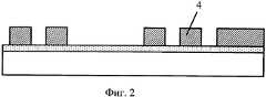
На Фиг.2 представлен схематический разрез структуры по прототипу после формирования горизонтальных проводников 4 методом локального травления.Figure 2 presents a schematic section of the structure of the prototype after the formation of
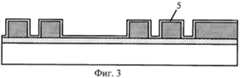
На Фиг.3 представлен схематический разрез структуры по прототипу после формирования защитного диэлектрика 5.Figure 3 presents a schematic section of the structure of the prototype after the formation of the
На Фиг.4 представлен схематический разрез структуры по прототипу после формирования пористого планаризующего диэлектрического слоя 6, покрывающего поверхность и заполняющего зазоры между горизонтальными проводниками.Figure 4 presents a schematic section of the structure of the prototype after the formation of a porous
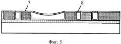
На Фиг.5 представлен схематический разрез структуры по прототипу после открытого травления пористого диэлектрического слоя в плазме до его удаления с поверхности над горизонтальными проводниками 7 и формирования на поверхности пористого слоя плотного поверхностного слоя 8 методом плазменной обработки.Figure 5 presents a schematic section of the structure of the prototype after open etching of the porous dielectric layer in the plasma before it is removed from the surface above the
На Фиг.6 представлен схематический разрез структуры по прототипу после нанесения межуровневого диэлектрического слоя 9.Figure 6 presents a schematic section of the structure of the prototype after applying the inter-level
На Фиг.7 представлен схематический разрез структуры по прототипу после формирования межуровневых отверстий 10 в диэлектрических слоях до поверхности горизонтальных проводников.Figure 7 presents a schematic section of the structure of the prototype after the formation of
На Фиг.8 представлен схематический разрез структуры по прототипу после нанесения второго проводящего слоя 11, покрывающего поверхность и заполняющего отверстия.On Fig presents a schematic section of the structure of the prototype after applying the second
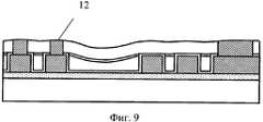
На Фиг.9 представлен схематический разрез структуры по прототипу после ХМП второго проводящего слоя до его удаления с поверхности диэлектрического слоя, в результате чего формируются межуровневые вертикальные проводники 12.Figure 9 presents a schematic section of the structure of the prototype after the CMP of the second conductive layer until it is removed from the surface of the dielectric layer, as a result of which inter-level
На Фиг.10-20 представлены основные этапы изготовления многоуровневых межсоединений интегральных микросхем с пористым диэлектрическим слоем в зазорах между проводниками по заявляемому способу на примере одного уровня горизонтальных и одного уровня вертикальных проводников.Figure 10-20 shows the main stages of the manufacture of multi-level interconnects of integrated circuits with a porous dielectric layer in the gaps between the conductors of the present method, using the example of one level of horizontal and one level of vertical conductors.
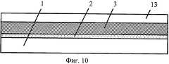
На Фиг.10 представлен схематический разрез структуры по заявляемому способу после нанесения на полупроводниковую подложку 1, покрытую диэлектрическим слоем 2, первого проводящего слой 3 и первого диэлектрического слоя 13.Figure 10 presents a schematic section of a structure according to the claimed method after applying to a
На Фиг.11 представлен схематический разрез структуры по заявляемому способу после локального травления межуровневых отверстий 10 в первом диэлектрическом слое.Figure 11 presents a schematic section of a structure according to the claimed method after local etching of
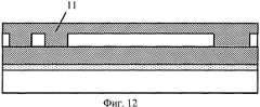
На Фиг.12 представлен схематический разрез структуры по заявляемому способу после формирования второго проводящего слоя 11, покрывающего поверхность и заполняющего межуровневые отверстия.On Fig presents a schematic section of a structure according to the claimed method after the formation of the second
На Фиг.13 представлен схематический разрез структуры по заявляемому способу после ХМП второго проводящего слоя до его удаления с поверхности первого диэлектрического слоя, в результате чего формируются межуровневые вертикальные проводники 12.On Fig presents a schematic section of the structure according to the claimed method after CMP of the second conductive layer until it is removed from the surface of the first dielectric layer, resulting in the formation of inter-level
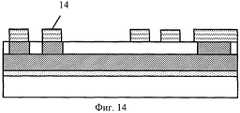
На Фиг.14 представлен схематический разрез структуры по заявляемому способу после формирования маски 14 с рисунком горизонтальных проводников.On Fig presents a schematic section of the structure of the present method after the formation of the
На Фиг.15 представлен схематический разрез структуры по заявляемому способу после локального травления первого диэлектрического слоя и первого проводящего слоя до диэлектрического слоя, покрывающего подложку, и удаления маски, в результате чего формируются горизонтальные проводники 4, разделенные зазорами, покрытые сверху первым диэлектрическим слоем, в который встроены вертикальные проводники.On Fig presents a schematic section of a structure according to the claimed method after local etching of the first dielectric layer and the first conductive layer to the dielectric layer covering the substrate, and removing the mask, resulting in the formation of
На Фиг.16 представлен схематический разрез структуры по заявляемому способу после формирования второго, защитного диэлектрического слоя 5.On Fig presents a schematic section of a structure according to the claimed method after the formation of the second,
На Фиг.17 представлен схематический разрез структуры по заявляемому способу после формирования третьего, пористого планаризующего диэлектрического слоя 6, покрывающего поверхность и заполняющего зазоры между смежными горизонтальными проводниками.On Fig presents a schematic section of a structure according to the claimed method after the formation of the third, porous
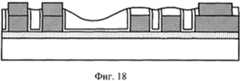
На Фиг.18 представлен схематический разрез структуры по заявляемому способу после открытого травления поверхности в плазме.On Fig presents a schematic section of a structure according to the claimed method after open etching of the surface in plasma.
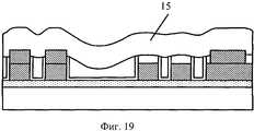
На Фиг.19 представлен схематический разрез структуры по заявляемому способу после формирования четвертого диэлектрического слоя 15.On Fig presents a schematic section of a structure according to the claimed method after the formation of the
На Фиг.20 представлен схематический разрез структуры по заявляемому способу после ХМП диэлектрических слоев до вскрытия поверхности вертикальных проводников 12.On Fig presents a schematic section of a structure according to the present method after CMP dielectric layers before opening the surface of the
Осуществление изобретения.The implementation of the invention.
На полупроводниковой подложке типа КЭФ4,5(100) с активными и пассивными элементами, покрытой диэлектрическим слоем толщиной 0,6 мкм и имеющей встроенные в диэлектрический слой вертикальные проводники на основе W, контактирующие с активными и пассивными элементами, формируют первый проводящий слой, состоящий из адгезионной пленки Ti толщиной 0,05 мкм, барьерной пленки TiN толщиной 0,1 мкм, проводящей пленки Аl, легированный Si и Сu. Методом плазмохимического осаждения из газовой смеси на основе моносилана и кислорода наносят первый диэлектрический слой толщиной 0,8 мкм. Формируют фоторезистивную маску под травление межуровневых отверстий. Минимальные отверстия имеют квадратную форму со стороной 0,6 мкм. Отверстия спроектированы так, что они симметрично перекрывают топологический края формируемых на последующих этапах проводников в направлении, перпендикулярном направлению вдоль проводников, на величину максимального рассовмещения слоев при формировании фоторезистивных масок, равную 0,05 мкм. Методом реактивного ионно-плазменного травления во фторсодержащей плазме вытравливают отверстия в первом диэлектрическом слое до первого проводящего слоя и удаляют маску в кислородсодержащей плазме. Формируют второй проводящий слой, состоящий из адгезионной пленки Ti толщиной 0,05 мкм, барьерной пленки TiN толщиной 0,1 мкм и проводящей пленки W толщиной 1,0 мкм, методом конформного газофазного осаждения. Удаляют второй проводящий слой с поверхности первого диэлектрического слоя методом ХМП. В результате формируют вольфрамовые вертикальные проводники, заполняющие межуровневые отверстия. Формируют фоторезистивную маску с рисунком горизонтальных проводников с минимальным зазором 0,35 мкм и минимальной шириной проводников 0,5 мкм. Вследствие рассовмещения слоев маска смещена относительно вольфрамовых проводников на величину до 0,05 мкм, в результате на части поверхности подложки край маски с одной стороны вольфрамовых проводников совпадает с их краем, а с противоположной стороны отстает от края на 0,1 мкм. Методом реактивного ионно-плазменного травления во фторсодержащей плазме локально травят первый диэлектрический слой до первого проводящего слоя селективно по отношению к W, TiN и Ti. Методом реактивного ионно-плазменного травления в хлорсодержащей плазме локально травят первый проводящий слой до диэлектрического слоя, покрывающего подложку селективно по отношению к W, TiN и Ti, и удаляют маску. В результате формируют горизонтальные проводники, покрытые сверху первым диэлектрическим слоем со встроенными в него вертикальными проводниками. Минимальный зазор между смежными горизонтальными проводниками 0,35 мкм, заложенный в топологию при проектировании, на части поверхности подложки в области межуровневых вертикальных вольфрамовых проводников минимального размера с одной из сторон проводников реально формируется меньшим на 0,1 мкм и составляет 0,25 мкм. Такой зазор формируется в области вдоль края вольфрамовых проводников минимального размера 0,6 мкм и не оказывает влияния на выход годных и суммарные паразитные емкостные связи между проводниками. Далее наносят третий, защитный диэлектрический слой диоксида кремния толщиной 0,03 мкм методом газофазного осаждения в плазме ВЧ-разряда из смеси на основе моносилана и кислорода. Методом химического нанесения из раствора, включающего нанесение пленки методом центрифугирования и термообработку, формируют планаризующий пористый диэлектрический слой, с ультранизкой диэлектрической проницаемостью Кэфф, равной 2,1, и размером пор от 0,002 до 0,05 мкм. Проводят операцию плазмохимического травления диэлектрических слоев во фторсодержащей плазме до их удаления с поверхности над горизонтальными проводниками с перетравом на глубину 0,4 мкм. Далее наносят четвертый диэлектрический слой толщиной 0,8 мкм газофазным методом и удаляют часть четвертого диэлектрического слоя методом ХМП до вскрытия поверхности вертикальных проводников. Цикл повторяют два раза начиная с формирования первого проводящего слоя. Далее наносят верхний проводящий слой, состоящий из адгезионной пленки Ti толщиной 0,05 мкм, барьерной пленки TiN толщиной 0,1 мкм, проводящей пленки Аl, легированный Si и Сu толщиной 0,8 мкм, формируют маску с рисунком верхних проводников, локально травят верхний проводящий слой и удаляют маску в кислородсодержащей плазме. Формируют слой пассивации путем осаждения диэлектрического слоя толщиной 0,03 мкм в плазме ВЧ-разряда из смеси на основе моносилана и закиси азота, нанесения пористого планаризующего диэлектрического слоя с ультранизкой диэлектрической проницаемостью методом химического нанесения из раствора и нанесения диэлектрического слоя толщиной 0,5 мкм в плазме ВЧ-разряда. Формируют в слое пассивации окна к площадкам для приварки выводов путем формирования фоторезистивной маски, локального плазмохимического травления слоя пассивации во фторсодержащей плазме и удаления маски, после чего проводят термообработку структур. В результате получают четыре уровня горизонтальных проводников, соединенных межуровневыми вертикальными проводниками, покрытые пассивирующим диэлектрическим слоем.On a KEF4.5 (100) type semiconductor substrate with active and passive elements coated with a 0.6 μm thick dielectric layer and having vertical W-based conductors embedded in the dielectric layer in contact with the active and passive elements, form a first conductive layer consisting of adhesive Ti film 0.05 μm thick, 0.1 μm TiN barrier film, conductive Al films doped with Si and Cu. By the method of plasma-chemical deposition from a gas mixture based on monosilane and oxygen, a first dielectric layer of 0.8 μm thickness is applied. A photoresist mask is formed under the etching of inter-level holes. Minimum holes are square in shape with a side of 0.6 μm. The holes are designed so that they symmetrically overlap the topological edges of the conductors formed at subsequent stages in the direction perpendicular to the direction along the conductors by the maximum misregistration of the layers during the formation of photoresist masks, equal to 0.05 μm. The method of reactive ion-plasma etching in a fluorine-containing plasma etches the holes in the first dielectric layer to the first conductive layer and removes the mask in the oxygen-containing plasma. A second conductive layer is formed, consisting of an adhesive Ti film of a thickness of 0.05 μm, a TiN barrier film of a thickness of 0.1 μm and a conductive film W of a thickness of 1.0 μm by conformal gas phase deposition. The second conductive layer is removed from the surface of the first dielectric layer by the CMP method. As a result, tungsten vertical conductors are formed filling inter-level holes. A photoresist mask is formed with a pattern of horizontal conductors with a minimum gap of 0.35 μm and a minimum width of conductors of 0.5 μm. Due to the misregistration of the layers, the mask is displaced relative to tungsten conductors by up to 0.05 μm, as a result, on the part of the substrate surface, the edge of the mask on one side of the tungsten conductors coincides with their edge, and on the opposite side it lags by 0.1 μm from the edge. By reactive ion-plasma etching in a fluorine-containing plasma, the first dielectric layer is locally etched to the first conductive layer selectively with respect to W, TiN and Ti. By reactive ion-plasma etching in a chlorine-containing plasma, the first conductive layer is locally etched to the dielectric layer covering the substrate selectively with respect to W, TiN and Ti, and the mask is removed. As a result, horizontal conductors are formed, coated on top of the first dielectric layer with vertical conductors embedded in it. The minimum gap between adjacent horizontal conductors of 0.35 μm, laid down in the design topology, on the part of the surface of the substrate in the region of inter-level vertical tungsten conductors of the minimum size, is actually formed smaller on one side of the conductors by 0.1 μm and is 0.25 μm. Such a gap is formed in the region along the edge of tungsten conductors of a minimum size of 0.6 μm and does not affect the yield and total stray capacitive coupling between the conductors. Next, a third, protective dielectric layer of silicon dioxide with a thickness of 0.03 μm is deposited by gas-phase deposition in an RF discharge plasma from a mixture based on monosilane and oxygen. By the method of chemical deposition from a solution, including the deposition of a film by centrifugation and heat treatment, a planarizing porous dielectric layer is formed with an ultra-low dielectric constant of Keff equal to 2.1 and a pore size of 0.002 to 0.05 μm. Plasma-chemical etching of dielectric layers in a fluorine-containing plasma is carried out until they are removed from the surface above horizontal conductors with grinding to a depth of 0.4 μm. Next, a fourth dielectric layer with a thickness of 0.8 μm is deposited by the gas-phase method and part of the fourth dielectric layer is removed by the CMP method until the surface of the vertical conductors is opened. The cycle is repeated two times starting from the formation of the first conductive layer. Then, an upper conductive layer is applied, consisting of an adhesive Ti film 0.05 μm thick, a 0.1 μm TiN barrier film, an Al film doped with Si and Cu 0.8 μm thick, a mask with a pattern of upper conductors is formed, the upper one is locally etched conductive layer and remove the mask in an oxygen-containing plasma. A passivation layer is formed by depositing a 0.03 μm thick dielectric layer in an RF discharge plasma from a mixture based on monosilane and nitrous oxide, applying a porous planarizing dielectric layer with an ultra-low dielectric constant by chemical deposition from a solution and applying a dielectric layer 0.5 μm thick in RF discharge plasma. The windows are formed in the passivation layer to the sites for welding the leads by forming a photoresist mask, local plasma-chemical etching of the passivation layer in the fluorine-containing plasma and removing the mask, after which the structures are heat treated. The result is four levels of horizontal conductors connected by inter-level vertical conductors, covered with a passivating dielectric layer.
Claims (12)
Translated fromRussianPriority Applications (1)
| Application Number | Priority Date | Filing Date | Title |
|---|---|---|---|
| RU2011110621/28ARU2459313C1 (en) | 2011-03-21 | 2011-03-21 | Method of making multilevel metallisation of integrated microcircuits with porous dielectric layer in gaps between conductors |
Applications Claiming Priority (1)
| Application Number | Priority Date | Filing Date | Title |
|---|---|---|---|
| RU2011110621/28ARU2459313C1 (en) | 2011-03-21 | 2011-03-21 | Method of making multilevel metallisation of integrated microcircuits with porous dielectric layer in gaps between conductors |
Publications (1)
| Publication Number | Publication Date |
|---|---|
| RU2459313C1true RU2459313C1 (en) | 2012-08-20 |
Family
ID=46936820
Family Applications (1)
| Application Number | Title | Priority Date | Filing Date |
|---|---|---|---|
| RU2011110621/28ARU2459313C1 (en) | 2011-03-21 | 2011-03-21 | Method of making multilevel metallisation of integrated microcircuits with porous dielectric layer in gaps between conductors |
Country Status (1)
| Country | Link |
|---|---|
| RU (1) | RU2459313C1 (en) |
Cited By (2)
| Publication number | Priority date | Publication date | Assignee | Title |
|---|---|---|---|---|
| RU2611098C1 (en)* | 2015-12-09 | 2017-02-21 | Акционерное общество "Научно-исследовательский институт молекулярной электроники" | Method of formation of multilevel metallization system based on tungsten for high-integrated circuits |
| RU2802797C1 (en)* | 2020-08-13 | 2023-09-04 | Чансинь Мемори Текнолоджис, Инк. | Method of manufacturing structure of bit bus, method of manufacturing semiconductor structure and semiconductor structure |
Citations (6)
| Publication number | Priority date | Publication date | Assignee | Title |
|---|---|---|---|---|
| SU1695777A1 (en)* | 1990-01-02 | 1994-07-30 | Научно-исследовательский институт молекулярной электроники | Method of manufacturing interconnections of integrated circuits |
| US5461003A (en)* | 1994-05-27 | 1995-10-24 | Texas Instruments Incorporated | Multilevel interconnect structure with air gaps formed between metal leads |
| EP0860879A2 (en)* | 1997-02-20 | 1998-08-26 | Nec Corporation | Multilevel interconnection in a semiconductor device and method for forming the same |
| US6051491A (en)* | 1995-10-17 | 2000-04-18 | Nec Corporation | Multilevel interconnection structure for integrated circuits and method of producing same |
| US6159842A (en)* | 1999-01-11 | 2000-12-12 | Taiwan Semiconductor Manufacturing Company | Method for fabricating a hybrid low-dielectric-constant intermetal dielectric (IMD) layer with improved reliability for multilevel interconnections |
| RU2230391C2 (en)* | 2002-03-21 | 2004-06-10 | Открытое акционерное общество "НИИ молекулярной электроники и завод "Микрон" | Process of manufacture of self-aligned built-in copper metallization of in tegrated circuits |
- 2011
- 2011-03-21RURU2011110621/28Apatent/RU2459313C1/enactive
Patent Citations (6)
| Publication number | Priority date | Publication date | Assignee | Title |
|---|---|---|---|---|
| SU1695777A1 (en)* | 1990-01-02 | 1994-07-30 | Научно-исследовательский институт молекулярной электроники | Method of manufacturing interconnections of integrated circuits |
| US5461003A (en)* | 1994-05-27 | 1995-10-24 | Texas Instruments Incorporated | Multilevel interconnect structure with air gaps formed between metal leads |
| US6051491A (en)* | 1995-10-17 | 2000-04-18 | Nec Corporation | Multilevel interconnection structure for integrated circuits and method of producing same |
| EP0860879A2 (en)* | 1997-02-20 | 1998-08-26 | Nec Corporation | Multilevel interconnection in a semiconductor device and method for forming the same |
| US6159842A (en)* | 1999-01-11 | 2000-12-12 | Taiwan Semiconductor Manufacturing Company | Method for fabricating a hybrid low-dielectric-constant intermetal dielectric (IMD) layer with improved reliability for multilevel interconnections |
| RU2230391C2 (en)* | 2002-03-21 | 2004-06-10 | Открытое акционерное общество "НИИ молекулярной электроники и завод "Микрон" | Process of manufacture of self-aligned built-in copper metallization of in tegrated circuits |
Cited By (2)
| Publication number | Priority date | Publication date | Assignee | Title |
|---|---|---|---|---|
| RU2611098C1 (en)* | 2015-12-09 | 2017-02-21 | Акционерное общество "Научно-исследовательский институт молекулярной электроники" | Method of formation of multilevel metallization system based on tungsten for high-integrated circuits |
| RU2802797C1 (en)* | 2020-08-13 | 2023-09-04 | Чансинь Мемори Текнолоджис, Инк. | Method of manufacturing structure of bit bus, method of manufacturing semiconductor structure and semiconductor structure |
Similar Documents
| Publication | Publication Date | Title |
|---|---|---|
| KR101018187B1 (en) | A method of electropolishing a metal layer on a wafer with trenches or vias using dummy structures | |
| US11367652B2 (en) | Microelectronic assembly from processed substrate | |
| US6297554B1 (en) | Dual damascene interconnect structure with reduced parasitic capacitance | |
| US4789648A (en) | Method for producing coplanar multi-level metal/insulator films on a substrate and for forming patterned conductive lines simultaneously with stud vias | |
| US6972253B2 (en) | Method for forming dielectric barrier layer in damascene structure | |
| US20040232552A1 (en) | Air gap dual damascene process and structure | |
| WO2001054190A1 (en) | Dielectric formation to seal porosity of etched low dielectric constant materials | |
| JP2009004665A (en) | Manufacturing method of semiconductor device | |
| JP3992654B2 (en) | Manufacturing method of semiconductor device | |
| US7544606B2 (en) | Method to implement stress free polishing | |
| CN100372113C (en) | Integrated circuit structure with air space and manufacturing method thereof | |
| WO2013040751A1 (en) | Method for forming air gap interconnect structure | |
| RU2459313C1 (en) | Method of making multilevel metallisation of integrated microcircuits with porous dielectric layer in gaps between conductors | |
| US20130161798A1 (en) | Graded density layer for formation of interconnect structures | |
| US6660618B1 (en) | Reverse mask and oxide layer deposition for reduction of vertical capacitance variation in multi-layer metallization systems | |
| US20100301494A1 (en) | Re-establishing a hydrophobic surface of sensitive low-k dielectrics in microstructure devices | |
| US6511904B1 (en) | Reverse mask and nitride layer deposition for reduction of vertical capacitance variation in multi-layer metallization systems | |
| JP2004363447A (en) | Semiconductor device and method of manufacturing the same | |
| CN104022071A (en) | Forming method of interconnection structure | |
| CN102403263A (en) | Trench etching method in double Damascus structure | |
| KR100688758B1 (en) | Method for forming gap fill for metal wiring in semiconductor device | |
| US6621290B1 (en) | Characterization of barrier layers in integrated circuit interconnects | |
| RU2436188C1 (en) | Method to manufacture multi-level interconnections of integral microcircuit chips with air gaps | |
| KR100955838B1 (en) | Semiconductor device and wiring manufacturing method | |
| WO2001054191A1 (en) | Damascene structure and method for forming a damascene structure |
Legal Events
| Date | Code | Title | Description |
|---|---|---|---|
| QB4A | Licence on use of patent | Free format text:LICENCE Effective date:20130801 |