RU2421742C1 - Device for contactless measurement of resistivity of silicon material - Google Patents
Device for contactless measurement of resistivity of silicon materialDownload PDFInfo
- Publication number
- RU2421742C1 RU2421742C1RU2010102282/28ARU2010102282ARU2421742C1RU 2421742 C1RU2421742 C1RU 2421742C1RU 2010102282/28 ARU2010102282/28 ARU 2010102282/28ARU 2010102282 ARU2010102282 ARU 2010102282ARU 2421742 C1RU2421742 C1RU 2421742C1
- Authority
- RU
- Russia
- Prior art keywords
- coil
- coils
- signal
- resistivity
- induced
- Prior art date
Links
Images


Landscapes
- Investigating Or Analyzing Materials By The Use Of Electric Means (AREA)
- Measurement Of Resistance Or Impedance (AREA)
- Investigating Or Analyzing Materials By The Use Of Magnetic Means (AREA)
Abstract
Description
Translated fromRussianИзобретение относится к области измерительной техники, более конкретно к области измерений электрофизических параметров полупроводниковых материалов с использованием эффекта электромагнитной индукции, и может быть использовано для определения удельного сопротивления кремниевого сырья, используемого в качестве шихты при выращивании монокристаллических слитков.The invention relates to the field of measuring technology, and more particularly to the field of measuring the electrophysical parameters of semiconductor materials using the effect of electromagnetic induction, and can be used to determine the resistivity of silicon raw materials used as a charge in the growth of single-crystal ingots.
Кремний является основным исходным материалом для солнечной энергетики. В последние годы вследствие существенно возросшего спроса на исходное сырье (поликристаллический кремний), обусловленного все возрастающим ростом производства кремниевых солнечных элементов (СЭ), наблюдается резкий дефицит сырья и соответственно рост стоимости кремния.Silicon is the main source material for solar energy. In recent years, due to a significantly increased demand for feedstock (polycrystalline silicon), due to the ever-increasing growth in the production of silicon solar cells (SC), there has been a sharp shortage of raw materials and, accordingly, an increase in the cost of silicon.
Все это делает экономически целесообразным вовлечение во вторичную переработку ранее неиспользуемых видов сырья: бой и брак пластин полупроводникового производства, кремниевая крошка, металлургический кремний, тигельные остатки ростового производства, тестовые и контрольные шайбы и т.п.All this makes it economically feasible to involve previously unused types of raw materials into the recycling process: battle and marriage of semiconductor production wafers, silicon chips, metallurgical silicon, crucible remnants of growth production, test and control washers, etc.
Основным методом переработки такого сырья является т.н. «перетяжка» по методу Чохральского: переплавка сортированного по типу проводимости сырья в слиток, колка выращенного слитка на фрагменты, сортировка фрагментов по удельному сопротивлению (для солнечного кремния это 0,005÷0,5 Ом·см и 0,5÷25 Ом·см) и выплавка из сортированного сырья монокристалла.The main processing method for such raw materials is the so-called “Hauling” according to the Czochralski method: remelting the sorted raw material by type of conductivity into an ingot, splitting the grown ingot into fragments, sorting fragments by resistivity (for solar silicon, this is 0.005 ÷ 0.5 Ohm · cm and 0.5 ÷ 25 Ohm · cm) and smelting from sorted raw materials of a single crystal.
Поскольку после колки слитка из переплавленного сырья кремний представляет собой куски неправильной формы, практически не имеющих протяженных плоских поверхностей, пригодных для контактных методов контроля (в том числе и частицы размером <<1 мм), сортировку осуществляют бесконтактным методом.Since after the ingot of the ingot from the remelted raw material is chopped, the silicon is irregularly shaped pieces, practically without extended flat surfaces, suitable for contact control methods (including particles with a size of << 1 mm), sorting is carried out by the non-contact method.
Известен способ локального контроля удельного сопротивления полупроводников и устройство для его осуществления, который основан на модуляции проводимости полупроводника точечным инжектирующим контактом, представляющим собой искру (шнур плазмы газового разряда диаметром ~20 мкм) между поверхностью полупроводника и отстоящим от нее металлическим острием [1].There is a method of local control of the resistivity of semiconductors and a device for its implementation, which is based on modulation of the conductivity of the semiconductor by a point injection contact, which is a spark (a gas discharge plasma cord with a diameter of ~ 20 μm) between the surface of the semiconductor and the metal tip spaced from it [1].
Амплитуда импульсов разрядного тока при разных полярностях металлического острия оказывается величиной, пропорциональной удельному сопротивлению измеряемого объекта.The amplitude of the discharge current pulses at different polarities of the metal tip turns out to be proportional to the resistivity of the measured object.
Поскольку величина искрового промежутка мала (<<1 мм), энергия искры недостаточна для эрозии поверхности полупроводника, поэтому метод можно считать неразрушающим и бесконтактным.Since the size of the spark gap is small (<< 1 mm), the spark energy is insufficient for erosion of the surface of the semiconductor, so the method can be considered non-destructive and non-contact.
Относительно высокая частота зондирующих импульсов (десятки герц) при использовании схемы накопления информации обеспечивает приемлемую точность измерений (±5÷±7%).The relatively high frequency of the probe pulses (tens of hertz) when using the information accumulation scheme provides acceptable measurement accuracy (± 5 ÷ ± 7%).
Способ имеет следующие недостатки:The method has the following disadvantages:
- способ пригоден в основном для сортировки объектов с протяженной гладкой поверхностью, высота неровностей на которых не превышает величину искрового промежутка (<<1 мм), позволяющей обеспечить стационарность режима разряда;- the method is mainly suitable for sorting objects with an extended smooth surface, the height of the irregularities on which does not exceed the value of the spark gap (<< 1 mm), which allows to ensure the stationary discharge mode;
- для достижения требуемой точности измерения необходима жесткая фиксация объекта измерения и металлического острия устройства для обеспечения стабилизации плазменного шнура.- to achieve the required measurement accuracy, rigid fixation of the measurement object and the metal tip of the device is necessary to ensure stabilization of the plasma cord.
Указанных недостатков лишено устройство бесконтактного измерения удельной проводимости полупроводниковых материалов, состоящее из датчика (катушки индуктивности), генератора высокочастотного сигнала, детектора индуцированного сигнала и устройства обработки выходного сигнала, в котором на расположенную в непосредственной близи от поверхности объекта измерения катушку индуктивности подается высокочастотный сигнал, а детектор индуцированного сигнала выделяет разностную ЭДС на катушке и по известному алгоритму преобразует его в величину удельного сопротивления образца [2].The indicated drawbacks are deprived of a non-contact device for measuring the specific conductivity of semiconductor materials, consisting of a sensor (inductor), a high-frequency signal generator, an induced signal detector, and an output signal processing device, in which a high-frequency signal is supplied to the inductor located in the immediate vicinity of the surface of the measurement object, and the induced signal detector selects the differential emf on the coil and, according to a known algorithm, converts it to Ichin resistivity of the sample [2].
Конструкция устройства и сущность метода поясняется фиг.1.The design of the device and the essence of the method is illustrated in figure 1.
При подаче на катушку 1 высокочастотного сигнала вокруг нее возникает электромагнитное поле 12, которое в полупроводниковом объекте измерения 11 наводит вихревые токи Фуко 13, которые, в свою очередь, меняют импеданс катушки 1.When a high-frequency signal is applied to coil 1, an electromagnetic field 12 arises around it, which induces Foucault eddy currents 13 in the
В результате этого изменения появляется дополнительная, или разностная, электродвижущая сила - ЭДС. Если образец отсутствует, то разностная ЭДС не возникает. Это изменение ЭДС выделяется в измерительном блоке устройства как величина, пропорциональная произведению толщины пластины d на ее удельную проводимость σ, т.е. регистрируется линейная зависимость этого произведенияAs a result of this change, an additional, or difference, electromotive force appears - EMF. If the sample is absent, then the differential EMF does not occur. This change in the EMF is highlighted in the measuring unit of the device as a value proportional to the product of the plate thickness d and its specific conductivity σ, i.e. linear relationship of this product is recorded

от величины выходного сигнала U.from the value of the output signal U.
Данный способ определения удельного сопротивления ρ полупроводникового материала (ρ=σ-1) является калибровочным и требует предварительной калибровки устройства путем экспериментального определения коэффициента пропорциональности k между выходным сигналом U и произведением удельной проводимости полупроводника на его толщину (d×σ), при этом предполагается, что полупроводник в области наведенных вихревых токов Фуко имеет гладкую протяженную поверхность.This method of determining the resistivity ρ of a semiconductor material (ρ = σ-1 ) is a calibration one and requires preliminary calibration of the device by experimentally determining the proportionality coefficient k between the output signal U and the product of the specific conductivity of the semiconductor by its thickness (d × σ), that the semiconductor in the region of induced eddy currents of Foucault has a smooth long surface.
Точность измерения данным устройством неодинакова для разных диапазонов величин удельного сопротивления:The measurement accuracy with this device is not the same for different ranges of resistivity values:
±15% - для диапазона 0,5÷25 Ом·см,± 15% - for the range of 0.5 ÷ 25 Ohm · cm,
±5% - для диапазона 0,005÷0,5 Ом·см.± 5% - for the range of 0.005 ÷ 0.5 Ohm · cm.
При измерении объектов, имеющих неправильную форму и развитую поверхность, погрешность измерений может достигать сотен процентов.When measuring objects having an irregular shape and developed surface, the measurement error can reach hundreds of percent.
Наиболее близким по технической сущности и достигаемому результату является устройство для бесконтактного измерения электрофизических параметров полупроводниковых материалов, состоящее из объекта измерения, устройства обработки сигнала, датчика, представляющего собой выполненные соосно генерирующую электромагнитное излучение катушку и регистрирующую индуцированное излучение катушку, причем генерирующая катушка расположена снаружи регистрирующей, а объект измерения находится внутри каркаса, на котором размещены катушки [3].The closest in technical essence and the achieved result is a device for non-contact measurement of the electrophysical parameters of semiconductor materials, consisting of a measurement object, a signal processing device, a sensor, which is a coil made coaxially generating electromagnetic radiation and detecting the induced radiation coil, and the generating coil is located outside the recording, and the measurement object is located inside the frame on which the coils are placed [3].
Конструкция устройства и сущность метода поясняется фиг.2.The design of the device and the essence of the method is illustrated in figure 2.
При прохождении через катушку 1 сигнала (переменного тока), генерируемого блоком 5, со скважностью, определяемой аналоговым ключом 4, катушка 1 генерируют переменное во времени электромагнитное поле, которое в свою очередь индуцирует наведенный сигнал в измерительной катушке 2. При помещении внутрь каркаса 3 образца (куска слитка полупроводникового материала) регистратор индуцированного сигнала 6 по известному алгоритму [4] из наведенного в катушке 2 потенциала U, пропорционального толщине образца d и удельной проводимости σ, выделяет либо составляющую удельной проводимости образцаWhen a signal (alternating current) generated by

либо составляющую толщины образцаor component of the thickness of the sample

которая индицируется измерительным прибором 7.which is indicated by the
Наименьшая погрешность измерений данным устройством (±5%) обеспечивается при условии, когда частотные характеристики генерирующей и измерительной катушек тождественны.The smallest measurement error with this device (± 5%) is provided provided that the frequency characteristics of the generating and measuring coils are identical.
К недостаткам данного устройства можно отнести следующее:The disadvantages of this device include the following:
- предельная точность измерений удельного сопротивления составляет ±5% вследствие того, что наведенный в измерительной катушке потенциал включает составляющую, обусловленную самоиндукцией в регистрирующей катушке;- the maximum accuracy of the measurements of resistivity is ± 5% due to the fact that the potential induced in the measuring coil includes a component due to self-induction in the recording coil;
- из-за того, что частотные характеристики реальных генерирующей и измерительной катушек всегда различны, для обеспечения точности измерений в пределах ±5% требуется калибровка устройства в узких диапазонах удельного сопротивления;- due to the fact that the frequency characteristics of real generating and measuring coils are always different, calibration of the device in narrow ranges of resistivity is required to ensure measurement accuracy within ± 5%;
- невозможность контроля объектов, представляющих собой сыпучий материал (смесь частицы с размером фракции <<1 мм).- the inability to control objects that represent bulk material (a mixture of particles with a fraction size of << 1 mm).
Задачей изобретения является повышение точности измерений и обеспечение контроля кремниевого сырья произвольной формы.The objective of the invention is to improve the accuracy of measurements and to ensure control of silicon raw materials of arbitrary shape.
Это достигается за счет того, что в устройстве для бесконтактного измерения удельного сопротивления кремниевого сырья, состоящем из датчика, представляющего собой цилиндрический контейнер из немагнитного материала, внутри которого размещен объект измерений, а на наружной боковой поверхности которого размещены первая и вторая катушки, генератора сигнала, с выходом которого скоммутирована первая катушка, регистратора индуцированного сигнала, со входом которого скоммутирована вторая катушка, первая и вторая катушки выполнены из немагнитного материала и представляют собой бифилярную катушку, причем первая и вторая катушки скоммутированы с генератором сигналов и регистратором индуцированного сигнала через дополнительно введенный в устройство двухканальный электронный переключатель, обеспечивающий перекоммутацию с заданной скважностью первой и второй катушек между генератором сигналов и регистратором индуцированного сигнала.This is achieved due to the fact that in the device for non-contact measurement of the resistivity of silicon raw materials, consisting of a sensor, which is a cylindrical container of non-magnetic material, inside which the measurement object is placed, and on the outer side surface of which the first and second coils of the signal generator are placed, with the output of which the first coil is connected, the induced signal recorder, with the input of which the second coil is connected, the first and second coils are made of non-magnetic of the total material and are a bifilar coil, the first and second coils being connected to the signal generator and the induced signal recorder via a two-channel electronic switch additionally inserted into the device, which provides switching with the given duty cycle of the first and second coils between the signal generator and the induced signal recorder.
Поскольку первая и вторая катушки выполнены в виде бифилярной катушки, и если намотка выполнена одинаковым проводом, параметры таких катушек (индуктивность и добротность) оказываются практически идентичными.Since the first and second coils are made in the form of a bifilar coil, and if the winding is made with the same wire, the parameters of such coils (inductance and quality factor) are almost identical.
Так как материал, из которого выполнены витки катушек, является немагнитным (например, медь или серебро), то коэффициент самоиндукции таких катушек практически равен нулю.Since the material from which the coils are made is non-magnetic (for example, copper or silver), the self-induction coefficient of such coils is practically zero.
Поскольку наведенная в катушке в режиме измерения ЭДС не содержит дополнительной составляющей, обусловленной эффектом самоиндукции, точность измерения удельного сопротивления ограничена только точностью обработки индуцированного сигнала, и достигает ±2,5÷±3,0%.Since the emf induced in the coil in the EMF measurement mode does not contain an additional component due to the self-induction effect, the accuracy of measuring the resistivity is limited only by the accuracy of processing the induced signal, and reaches ± 2.5 ÷ ± 3.0%.
Незначительные отличия в конструктивных особенностях изготовления катушек (сдвиг межвиткового расстояния, смещение витков и пр.) практически нивелируются за счет попеременного использования катушек в качестве генерирующей сигнал и регистрирующей индуцированный сигнал объекта, что обеспечивается использованием в устройстве двухканального электронного переключателя.Slight differences in the design features of the manufacture of coils (inter-turn distance shift, coil displacement, etc.) are practically eliminated due to the alternate use of the coils as a signal-generating and recording object-induced signal, which is ensured by the use of a two-channel electronic switch in the device.
В известных науке и технике решениях аналогичной задачи не обнаружено попеременное использование индуцирующей электромагнитный сигнал и регистрирующей индуцированный сигнал катушек, выполненных в виде бифилярной катушки из немагнитного материала, поэтому все заявляемые отличия данного изобретения соответствуют критерию "Изобретательский уровень".In the known science and technology solutions to a similar problem, the alternate use of electromagnetic coil inducing electromagnetic signal and detecting the induced signal coils made in the form of a bifilar coil of non-magnetic material is not found, therefore, all the claimed differences of this invention meet the criterion of "Inventive step".
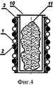
Сущность изобретения поясняется фиг.3 и фиг.4, где:The invention is illustrated in figure 3 and figure 4, where:
1 - первая катушка;1 - the first coil;
2 - вторая катушка;2 - second coil;
3 - цилиндрический контейнер диаметром d;3 - a cylindrical container with a diameter d;
4 - аналоговый ключ;4 - an analog key;
5 - генератор сигналов;5 - signal generator;
6 - регистратор индуцированного сигнала;6 - recorder induced signal;
7 - индикатор;7 - indicator;
8 - внутренняя полость контейнера;8 - the internal cavity of the container;
9 - двухканальный электронный переключатель;9 - two-channel electronic switch;
10 - съемный пластиковый контейнер;10 - removable plastic container;
11 - объект измерения,11 - measurement object,
и заключается в следующем.and is as follows.
Внутри датчика, представляющего собой цилиндрический контейнер 3 из немагнитного материала, на наружной боковой поверхности которого размещены первая 1 и вторая 2 катушки, размещен в съемном пластиковом контейнере 10 объект измерений 11. Генератор сигналов 5 с заданной скважностью, определяемой аналоговым ключом 4, посылает на обмотку катушки 1 (или катушки 2, если она в данный момент времени скоммутирована двухканальным электронным переключателем 9 с выходом генератора сигналов 5) ВЧ-сигнал, а регистратор индуцированного сигнала 6 регистрирует индуцированный в катушке 2 сигнал (или в катушке 1, если она в данный момент времени скоммутирована двухканальным электронным переключателем 9 со входом регистратора индуцированного сигнала 6), анализирует ЭДС на катушках при подаче ВЧ-сигнала и в периоды между ВЧ-сигналами, выделяет разностный сигнал, обрабатывает его по известному алгоритму [4], а результат обработки в виде значения удельного сопротивления образца 11, находящегося внутри датчика, выводится на шкалу индикатора 7.Inside the sensor, which is a
Контейнер 3 и катушки 1 и 2 выполнены из немагнитных материалов (например, из пластика и медной проволоки соответственно). Катушки 1 и 2 попеременно выполняют функции генератора электромагнитного излучения и регистратора индуцированного сигнала.The
Разностный сигнал несет в себе информацию о величине удельного сопротивления полупроводникового материала и практически не зависит от степени шероховатости поверхности полупроводникового материала.The difference signal carries information about the value of the resistivity of the semiconductor material and is practically independent of the degree of surface roughness of the semiconductor material.
Величина индуцированного электромагнитного поля в полупроводниковом объекте экспоненциально спадает с увеличением расстояния от этой поверхности. При этом постоянная затухания λ индуцированного поля имеет видThe magnitude of the induced electromagnetic field in a semiconductor object decreases exponentially with increasing distance from this surface. In this case, the damping constant λ of the induced field has the form

где: h - расстояние от поверхности полупроводникового образца,where: h is the distance from the surface of the semiconductor sample,
L - глубина скин-слоя электромагнитного поля в объеме образца.L is the depth of the skin layer of the electromagnetic field in the sample volume.
Глубина скин-слоя, в свою очередь, зависит от частоты электромагнитных колебаний, поэтому выбрав частоту, для которой обеспечивается условие λ<<1, и разлагая экспоненту в ряд до линейного члена разложения, мы приходим к условию исключения влияния неконтролируемого рельефа поверхности.The depth of the skin layer, in turn, depends on the frequency of electromagnetic oscillations, therefore, choosing the frequency for which the condition λ << 1 is satisfied, and expanding the exponent in a row to the linear term of the expansion, we come to the condition of eliminating the influence of an uncontrolled surface topography.
Очевидно, что полностью исключить влияние шероховатости поверхности на результат измерений в такой схеме измерений невозможно, но ошибку этого влияния можно минимизировать до любой заданной величины при варьировании частоты колебаний электромагнитного поля.Obviously, it is impossible to completely exclude the influence of surface roughness on the measurement result in such a measurement scheme, but the error of this effect can be minimized to any given value by varying the frequency of electromagnetic field oscillations.
Очевидно, что минимальная погрешность измерений обеспечивается на объектах, форма которых наиболее приближена к цилиндрической (например, кремниевое сырье в виде частиц с размером фракции до 1 мм, помещенное в пластиковый цилиндрический контейнер).Obviously, the minimum measurement error is ensured at objects whose shape is closest to cylindrical (for example, silicon raw materials in the form of particles with a fraction size of up to 1 mm placed in a plastic cylindrical container).
Влияние на результаты измерений геометрических особенностей катушки минимизировано, т.к. используемые в качестве генератора ВЧ-сигнала и регистратора индуцированного сигнала катушки выполнены в виде бифилярной катушки, их намотка выполнена одинаковым проводом, и параметры таких катушек (индуктивность и добротность) оказываются практически идентичными.The influence on the measurement results of the geometric features of the coil is minimized, because the coils used as the generator of the RF signal and the registrar of the induced signal are made in the form of a bifilar coil, they are wound with the same wire, and the parameters of such coils (inductance and quality factor) are almost identical.
Поскольку материал, из которого выполнены витки катушек, является немагнитным (например, медь или серебро), то коэффициент самоиндукции таких катушек практически равен нулю.Since the material from which the coils are made is non-magnetic (for example, copper or silver), the self-induction coefficient of such coils is practically zero.
Экспериментально установлено, что достаточно двух частотных интервалов для обеспечения измерений в интервале удельных сопротивлений кремниевого сырья ρ=0,01÷25,0 Ом·см (для измерения удельного сопротивления в интервале ρ=1,0÷25,0 Ом·см используется частота 100 кГц, а для измерений удельного сопротивления в интервале ρ=0,01÷1,0 Ом·см - частота 25 кГц). В целом, заявляемое устройство позволяет проводить измерение удельного сопротивления кремниевого сырья любой конфигурации (в том числе и мелкой фракции с размером зерна ≤1 мм) с относительной точностью ±2,5% во всем интервале заданных удельных сопротивлений.It was experimentally established that two frequency intervals are sufficient to ensure measurements in the range of specific resistivities of silicon raw materials ρ = 0.01 ÷ 25.0 Ohm · cm (for measuring resistivity in the range ρ = 1.0 ÷ 25.0 Ohm · cm 100 kHz, and for measurements of resistivity in the range ρ = 0.01 ÷ 1.0 Ohm · cm - frequency 25 kHz). In General, the inventive device allows you to measure the resistivity of silicon raw materials of any configuration (including fine fractions with grain size ≤1 mm) with a relative accuracy of ± 2.5% in the entire range of specified resistivities.
Пример конкретного выполненияConcrete example
Конструкция устройства поясняется фиг.3 и фиг.4.The design of the device is illustrated in figure 3 and figure 4.
Внутри датчика, представляющего собой цилиндрический контейнер 3 из немагнитного материала (текстолита), на наружной боковой поверхности которого размещены первая 1 и вторая 2 катушки, помещают в съемном пластиковом контейнере 10 объект измерений 11.Inside the sensor, which is a
Диаметр пластикового контейнера - 25 мм, высота - 45 мм.The diameter of the plastic container is 25 mm, the height is 45 mm.
Катушки 1 и 2 выполнены бифилярной намоткой из медной проволоки диаметром 0,4 мм и содержат по 6 полных витков, длина катушки - 45 мм. Бифилярная катушка расположена на внешней поверхности цилиндрического текстолитового контейнера 3 диаметром d=30 мм и уложена в спиральной канавке на поверхности контейнера (для обеспечения постоянного шага между витками).
В качестве объекта измерения использован кусок монокристаллического кремния из тигельных остатков процесса выращивания монокристаллов марки КДБ-10, т.е. предполагаемый диапазон измерений удельного сопротивления кремния должен соответствовать значениям 0,5÷25 Ом·см.A piece of monocrystalline silicon from crucible residues of the process of growing single crystals of the KDB-10 brand, i.e. the expected range of measurements of the resistivity of silicon should correspond to values of 0.5 ÷ 25 Ohm · cm.
Для указанного диапазона частота ВЧ-сигнала генератора сигналов 5 составляет 100 кГц, скважность сигнала, определяемая аналоговым ключом 4, составляла 50 Гц.For the indicated range, the frequency of the RF signal of
Перекоммутация катушек 1 и 2 двухканальным электронным переключателем 9 осуществляется со скважностью ~0,1 сек.The switching of
Выходной сигнал от катушки, скоммутированной в конкретный момент времени со входом регистратора индуцированного сигнала 6, с задержкой на время установления переходных процессов переключения поступает на вход регистратора индуцированного сигнала 6, который анализирует ЭДС на катушках при подаче ВЧ-сигнала и в периоды между ВЧ-сигналами, выделяет разностный сигнал, обрабатывает его по известному алгоритму, а результат обработки в виде значения удельного сопротивления образца 11, находящегося внутри датчика, выводятся на шкалу индикатора 7.The output signal from the coil, connected at a particular moment in time with the input of the induced
Измерение удельного сопротивления осуществляется следующим образом. Объект измерения 11 неправильной продолговатой формы с развитой поверхностью, не имеющий протяженных плоских участков поверхности (кусок из сплавленного тигельного остатка из процесса выращивания монокристаллического слитка кремния марки КДБ-10 (111)-4°), помещают в съемный пластиковый контейнер 10, загруженный контейнер помещают во внутреннюю полость контейнера 8, включают питание генератора сигналов 5 и регистратора индуцированного сигнала 6.The measurement of resistivity is as follows.
В течение нескольких секунд (от 2 до 5 сек) регистратор индуцированного сигнала 6 повторяет процесс выделения разностного сигнала, после чего сигнал усредняется, обрабатывается и на индикатор 7 выводится выделенное регистратором индуцированного сигнала 6 значение удельного сопротивления (в данном примере эта величина составила 13,6 Ом·см).Within a few seconds (from 2 to 5 seconds), the induced
После считывания результата измерения оператор вынимает контейнер 10, измеряемый объект 11 извлекается и помещается в соответствующую измеренному значению удельного сопротивления емкость, в контейнер 10 загружается следующий образец, и процесс повторяется.After reading the measurement result, the operator takes out the
Вышеописанное выполнение измерительного устройства обеспечивает возможность воспроизводимого и неразрушающего измерения удельного сопротивления кремниевого сырья неправильной формы, в том числе и мелкодисперсной фракции, и обеспечивает сортировку кремниевого сырья по удельному сопротивлению с точностью до ±2,5%, что делает возможным его повторное использование в полупроводниковом производстве.The described embodiment of the measuring device provides the possibility of reproducible and non-destructive measurement of the resistivity of irregularly shaped silicon raw materials, including the finely divided fraction, and enables the silicon raw materials to be sorted by specific resistance with an accuracy of ± 2.5%, which makes it possible to reuse them in semiconductor manufacturing .
Источники информацииInformation sources
1. Авторское свидетельство СССР. МПК: G01N 27/62, №1822972 от 23.06.1993.1. Copyright certificate of the USSR. IPC: G01N 27/62, No. 1822972 of 06.23.1993.
2. Патент США. МПК: G01R 27/00, №6,657,439 B1 от 02 декабря 2003 г.2. US patent. IPC: G01R 27/00, No. 6,657,439 B1 dated December 2, 2003.
3. Патент США. МПК: G01N 27/72, №6,661,224 от 09 декабря 2003 г. - прототип.3. US patent. IPC: G01N 27/72, No. 6,661,224 of December 9, 2003 - prototype.
4. Патент США. МПК: G01R 31/265, №4,286,215 от 25 августа 1981 г.4. US patent. IPC: G01R 31/265, No. 4.286.215 of August 25, 1981
Claims (1)
Translated fromRussianPriority Applications (1)
| Application Number | Priority Date | Filing Date | Title |
|---|---|---|---|
| RU2010102282/28ARU2421742C1 (en) | 2010-01-27 | 2010-01-27 | Device for contactless measurement of resistivity of silicon material |
Applications Claiming Priority (1)
| Application Number | Priority Date | Filing Date | Title |
|---|---|---|---|
| RU2010102282/28ARU2421742C1 (en) | 2010-01-27 | 2010-01-27 | Device for contactless measurement of resistivity of silicon material |
Publications (1)
| Publication Number | Publication Date |
|---|---|
| RU2421742C1true RU2421742C1 (en) | 2011-06-20 |
Family
ID=44738131
Family Applications (1)
| Application Number | Title | Priority Date | Filing Date |
|---|---|---|---|
| RU2010102282/28ARU2421742C1 (en) | 2010-01-27 | 2010-01-27 | Device for contactless measurement of resistivity of silicon material |
Country Status (1)
| Country | Link |
|---|---|
| RU (1) | RU2421742C1 (en) |
Cited By (3)
| Publication number | Priority date | Publication date | Assignee | Title |
|---|---|---|---|---|
| RU2534728C1 (en)* | 2013-05-30 | 2014-12-10 | Федеральное Государственное Бюджетное Образовательное Учреждение Высшего Профессионального Образования "Саратовский Государственный Университет Имени Н.Г. Чернышевского" | Device for determination of parameters of metal-dielectric structures |
| RU168724U1 (en)* | 2016-06-07 | 2017-02-17 | федеральное государственное автономное образовательное учреждение высшего образования "Самарский национальный исследовательский университет имени академика С.П. Королева" | Non-contact control device for electromagnetic parameters of thin films |
| RU2729169C1 (en)* | 2020-02-03 | 2020-08-04 | федеральное государственное бюджетное образовательное учреждение высшего образования "Санкт-Петербургский горный университет" | Device for measuring specific resistance of semiconductor cutting ceramic plates |
Citations (4)
| Publication number | Priority date | Publication date | Assignee | Title |
|---|---|---|---|---|
| US4000458A (en)* | 1975-08-21 | 1976-12-28 | Bell Telephone Laboratories, Incorporated | Method for the noncontacting measurement of the electrical conductivity of a lamella |
| US4286215A (en)* | 1979-05-18 | 1981-08-25 | Bell Telephone Laboratories, Incorporated | Method and apparatus for the contactless monitoring carrier lifetime in semiconductor materials |
| US4849694A (en)* | 1986-10-27 | 1989-07-18 | Nanometrics, Incorporated | Thickness measurements of thin conductive films |
| US6661224B1 (en)* | 1999-06-30 | 2003-12-09 | Abb Ab | Method for inductive measurement of a dimension of an object |
- 2010
- 2010-01-27RURU2010102282/28Apatent/RU2421742C1/ennot_activeIP Right Cessation
Patent Citations (4)
| Publication number | Priority date | Publication date | Assignee | Title |
|---|---|---|---|---|
| US4000458A (en)* | 1975-08-21 | 1976-12-28 | Bell Telephone Laboratories, Incorporated | Method for the noncontacting measurement of the electrical conductivity of a lamella |
| US4286215A (en)* | 1979-05-18 | 1981-08-25 | Bell Telephone Laboratories, Incorporated | Method and apparatus for the contactless monitoring carrier lifetime in semiconductor materials |
| US4849694A (en)* | 1986-10-27 | 1989-07-18 | Nanometrics, Incorporated | Thickness measurements of thin conductive films |
| US6661224B1 (en)* | 1999-06-30 | 2003-12-09 | Abb Ab | Method for inductive measurement of a dimension of an object |
Cited By (3)
| Publication number | Priority date | Publication date | Assignee | Title |
|---|---|---|---|---|
| RU2534728C1 (en)* | 2013-05-30 | 2014-12-10 | Федеральное Государственное Бюджетное Образовательное Учреждение Высшего Профессионального Образования "Саратовский Государственный Университет Имени Н.Г. Чернышевского" | Device for determination of parameters of metal-dielectric structures |
| RU168724U1 (en)* | 2016-06-07 | 2017-02-17 | федеральное государственное автономное образовательное учреждение высшего образования "Самарский национальный исследовательский университет имени академика С.П. Королева" | Non-contact control device for electromagnetic parameters of thin films |
| RU2729169C1 (en)* | 2020-02-03 | 2020-08-04 | федеральное государственное бюджетное образовательное учреждение высшего образования "Санкт-Петербургский горный университет" | Device for measuring specific resistance of semiconductor cutting ceramic plates |
Similar Documents
| Publication | Publication Date | Title |
|---|---|---|
| US4528856A (en) | Eddy current stress-strain gauge | |
| Tsukada et al. | Detection of inner corrosion of steel construction using magnetic resistance sensor and magnetic spectroscopy analysis | |
| RU2421742C1 (en) | Device for contactless measurement of resistivity of silicon material | |
| RU2420749C1 (en) | Device for noncontact measurement of specific resistance of semiconductor materials | |
| CN101561466B (en) | A method for measuring eddy current conductivity | |
| US4803428A (en) | Method and apparatus for non-destructive material testing, particularly for determination of thickness of coating layers on a base material by measuring electrical conductivity or magnetic permeability at the finished specimen | |
| JP3707547B2 (en) | Method for measuring Si concentration in steel material and method for producing electrical steel sheet | |
| Faraj et al. | Construct coil probe using GMR sensor for eddy current testing | |
| JPS62273447A (en) | Method and apparatus for measuring deterioration degree of material | |
| JPH07198770A (en) | Improved probe device and method for measuring critical superconducting current in non-contacting state | |
| RU2566416C1 (en) | Device for eddy-current magnetic examination of ferromagnetic objects | |
| EP1709453B1 (en) | Method to forecast the electrical conductivity of anodes for aluminum production before baking | |
| Dziczkowski | Effect of eddy current frequency on measuring properties of devices used in non-destructive measurements of non-ferromagnetic metal plates | |
| SU875265A1 (en) | Method of determining resistance of solid alloys to wear | |
| Boley et al. | Capacitance bridge measurements of magnetostriction | |
| Takahashi et al. | Development of the 2-D single-sheet tester using diagonal exciting coil and the measurement of magnetic properties of grain-oriented electrical steel sheet | |
| Lugovskoy et al. | Investigation of welds by the method of the magneto-optical eddy current flaw detection | |
| Ibragimov et al. | Measuring stresses in welded joints by the remagnetisation loss method | |
| JPWO2006059497A1 (en) | Method and device for measuring critical current density of superconductor | |
| RU2087994C1 (en) | Method for measuring critical current of high- temperature superconducting material y-ba-cu-o | |
| Sonoda et al. | Measurement of fluctuations of magnetized loop in amorphous cores | |
| Moutoussamy et al. | Feasibility of a Giant MagnetoImpedance Sandwich magnetometer for space applications | |
| Augutis et al. | Determination of metal surface hardened layer depth using magnetic Barkhausen noise | |
| RU2778801C1 (en) | Method for magnetic particle testing of articles made of ferromagnetic materials and magnetic particle testing unit for implementation thereof | |
| JP3223991U (en) | Nondestructive inspection equipment |
Legal Events
| Date | Code | Title | Description |
|---|---|---|---|
| MM4A | The patent is invalid due to non-payment of fees | Effective date:20160128 |