RU2419740C1 - Highlighter and flat display with said highlighter - Google Patents
Highlighter and flat display with said highlighterDownload PDFInfo
- Publication number
- RU2419740C1 RU2419740C1RU2009134481/28ARU2009134481ARU2419740C1RU 2419740 C1RU2419740 C1RU 2419740C1RU 2009134481/28 ARU2009134481/28 ARU 2009134481/28ARU 2009134481 ARU2009134481 ARU 2009134481ARU 2419740 C1RU2419740 C1RU 2419740C1
- Authority
- RU
- Russia
- Prior art keywords
- point light
- light source
- conductor
- metal core
- heat dissipating
- Prior art date
Links
Images


Classifications
- G—PHYSICS
- G02—OPTICS
- G02B—OPTICAL ELEMENTS, SYSTEMS OR APPARATUS
- G02B6/00—Light guides; Structural details of arrangements comprising light guides and other optical elements, e.g. couplings
- G02B6/0001—Light guides; Structural details of arrangements comprising light guides and other optical elements, e.g. couplings specially adapted for lighting devices or systems
- G02B6/0011—Light guides; Structural details of arrangements comprising light guides and other optical elements, e.g. couplings specially adapted for lighting devices or systems the light guides being planar or of plate-like form
- G02B6/0066—Light guides; Structural details of arrangements comprising light guides and other optical elements, e.g. couplings specially adapted for lighting devices or systems the light guides being planar or of plate-like form characterised by the light source being coupled to the light guide
- G02B6/0073—Light emitting diode [LED]
- G—PHYSICS
- G02—OPTICS
- G02B—OPTICAL ELEMENTS, SYSTEMS OR APPARATUS
- G02B6/00—Light guides; Structural details of arrangements comprising light guides and other optical elements, e.g. couplings
- G02B6/0001—Light guides; Structural details of arrangements comprising light guides and other optical elements, e.g. couplings specially adapted for lighting devices or systems
- G02B6/0011—Light guides; Structural details of arrangements comprising light guides and other optical elements, e.g. couplings specially adapted for lighting devices or systems the light guides being planar or of plate-like form
- G02B6/0081—Mechanical or electrical aspects of the light guide and light source in the lighting device peculiar to the adaptation to planar light guides, e.g. concerning packaging
- G02B6/0083—Details of electrical connections of light sources to drivers, circuit boards, or the like
- G—PHYSICS
- G02—OPTICS
- G02B—OPTICAL ELEMENTS, SYSTEMS OR APPARATUS
- G02B6/00—Light guides; Structural details of arrangements comprising light guides and other optical elements, e.g. couplings
- G02B6/0001—Light guides; Structural details of arrangements comprising light guides and other optical elements, e.g. couplings specially adapted for lighting devices or systems
- G02B6/0011—Light guides; Structural details of arrangements comprising light guides and other optical elements, e.g. couplings specially adapted for lighting devices or systems the light guides being planar or of plate-like form
- G02B6/0081—Mechanical or electrical aspects of the light guide and light source in the lighting device peculiar to the adaptation to planar light guides, e.g. concerning packaging
- G02B6/0085—Means for removing heat created by the light source from the package
- H—ELECTRICITY
- H05—ELECTRIC TECHNIQUES NOT OTHERWISE PROVIDED FOR
- H05K—PRINTED CIRCUITS; CASINGS OR CONSTRUCTIONAL DETAILS OF ELECTRIC APPARATUS; MANUFACTURE OF ASSEMBLAGES OF ELECTRICAL COMPONENTS
- H05K1/00—Printed circuits
- H05K1/02—Details
- H05K1/0201—Thermal arrangements, e.g. for cooling, heating or preventing overheating
- H05K1/0203—Cooling of mounted components
- H05K1/0209—External configuration of printed circuit board adapted for heat dissipation, e.g. lay-out of conductors, coatings
- G—PHYSICS
- G02—OPTICS
- G02B—OPTICAL ELEMENTS, SYSTEMS OR APPARATUS
- G02B6/00—Light guides; Structural details of arrangements comprising light guides and other optical elements, e.g. couplings
- G02B6/0001—Light guides; Structural details of arrangements comprising light guides and other optical elements, e.g. couplings specially adapted for lighting devices or systems
- G02B6/0011—Light guides; Structural details of arrangements comprising light guides and other optical elements, e.g. couplings specially adapted for lighting devices or systems the light guides being planar or of plate-like form
- G02B6/0066—Light guides; Structural details of arrangements comprising light guides and other optical elements, e.g. couplings specially adapted for lighting devices or systems the light guides being planar or of plate-like form characterised by the light source being coupled to the light guide
- G02B6/0068—Arrangements of plural sources, e.g. multi-colour light sources
- G—PHYSICS
- G02—OPTICS
- G02F—OPTICAL DEVICES OR ARRANGEMENTS FOR THE CONTROL OF LIGHT BY MODIFICATION OF THE OPTICAL PROPERTIES OF THE MEDIA OF THE ELEMENTS INVOLVED THEREIN; NON-LINEAR OPTICS; FREQUENCY-CHANGING OF LIGHT; OPTICAL LOGIC ELEMENTS; OPTICAL ANALOGUE/DIGITAL CONVERTERS
- G02F1/00—Devices or arrangements for the control of the intensity, colour, phase, polarisation or direction of light arriving from an independent light source, e.g. switching, gating or modulating; Non-linear optics
- G02F1/01—Devices or arrangements for the control of the intensity, colour, phase, polarisation or direction of light arriving from an independent light source, e.g. switching, gating or modulating; Non-linear optics for the control of the intensity, phase, polarisation or colour
- G02F1/13—Devices or arrangements for the control of the intensity, colour, phase, polarisation or direction of light arriving from an independent light source, e.g. switching, gating or modulating; Non-linear optics for the control of the intensity, phase, polarisation or colour based on liquid crystals, e.g. single liquid crystal display cells
- G02F1/133—Constructional arrangements; Operation of liquid crystal cells; Circuit arrangements
- G02F1/1333—Constructional arrangements; Manufacturing methods
- G02F1/1335—Structural association of cells with optical devices, e.g. polarisers or reflectors
- G02F1/1336—Illuminating devices
- G02F1/133615—Edge-illuminating devices, i.e. illuminating from the side
- H—ELECTRICITY
- H05—ELECTRIC TECHNIQUES NOT OTHERWISE PROVIDED FOR
- H05K—PRINTED CIRCUITS; CASINGS OR CONSTRUCTIONAL DETAILS OF ELECTRIC APPARATUS; MANUFACTURE OF ASSEMBLAGES OF ELECTRICAL COMPONENTS
- H05K1/00—Printed circuits
- H05K1/18—Printed circuits structurally associated with non-printed electric components
- H05K1/189—Printed circuits structurally associated with non-printed electric components characterised by the use of a flexible or folded printed circuit
- H—ELECTRICITY
- H05—ELECTRIC TECHNIQUES NOT OTHERWISE PROVIDED FOR
- H05K—PRINTED CIRCUITS; CASINGS OR CONSTRUCTIONAL DETAILS OF ELECTRIC APPARATUS; MANUFACTURE OF ASSEMBLAGES OF ELECTRICAL COMPONENTS
- H05K2201/00—Indexing scheme relating to printed circuits covered by H05K1/00
- H05K2201/09—Shape and layout
- H05K2201/09209—Shape and layout details of conductors
- H05K2201/0929—Conductive planes
- H05K2201/09363—Conductive planes wherein only contours around conductors are removed for insulation
- H—ELECTRICITY
- H05—ELECTRIC TECHNIQUES NOT OTHERWISE PROVIDED FOR
- H05K—PRINTED CIRCUITS; CASINGS OR CONSTRUCTIONAL DETAILS OF ELECTRIC APPARATUS; MANUFACTURE OF ASSEMBLAGES OF ELECTRICAL COMPONENTS
- H05K2201/00—Indexing scheme relating to printed circuits covered by H05K1/00
- H05K2201/09—Shape and layout
- H05K2201/09209—Shape and layout details of conductors
- H05K2201/09654—Shape and layout details of conductors covering at least two types of conductors provided for in H05K2201/09218 - H05K2201/095
- H05K2201/09781—Dummy conductors, i.e. not used for normal transport of current; Dummy electrodes of components
- H—ELECTRICITY
- H05—ELECTRIC TECHNIQUES NOT OTHERWISE PROVIDED FOR
- H05K—PRINTED CIRCUITS; CASINGS OR CONSTRUCTIONAL DETAILS OF ELECTRIC APPARATUS; MANUFACTURE OF ASSEMBLAGES OF ELECTRICAL COMPONENTS
- H05K2201/00—Indexing scheme relating to printed circuits covered by H05K1/00
- H05K2201/10—Details of components or other objects attached to or integrated in a printed circuit board
- H05K2201/10007—Types of components
- H05K2201/10106—Light emitting diode [LED]
- H—ELECTRICITY
- H05—ELECTRIC TECHNIQUES NOT OTHERWISE PROVIDED FOR
- H05K—PRINTED CIRCUITS; CASINGS OR CONSTRUCTIONAL DETAILS OF ELECTRIC APPARATUS; MANUFACTURE OF ASSEMBLAGES OF ELECTRICAL COMPONENTS
- H05K2201/00—Indexing scheme relating to printed circuits covered by H05K1/00
- H05K2201/10—Details of components or other objects attached to or integrated in a printed circuit board
- H05K2201/10613—Details of electrical connections of non-printed components, e.g. special leads
- H05K2201/10954—Other details of electrical connections
- H05K2201/10969—Metallic case or integral heatsink of component electrically connected to a pad on PCB
- H—ELECTRICITY
- H05—ELECTRIC TECHNIQUES NOT OTHERWISE PROVIDED FOR
- H05K—PRINTED CIRCUITS; CASINGS OR CONSTRUCTIONAL DETAILS OF ELECTRIC APPARATUS; MANUFACTURE OF ASSEMBLAGES OF ELECTRICAL COMPONENTS
- H05K2201/00—Indexing scheme relating to printed circuits covered by H05K1/00
- H05K2201/20—Details of printed circuits not provided for in H05K2201/01 - H05K2201/10
- H05K2201/2054—Light-reflecting surface, e.g. conductors, substrates, coatings, dielectrics
- H—ELECTRICITY
- H05—ELECTRIC TECHNIQUES NOT OTHERWISE PROVIDED FOR
- H05K—PRINTED CIRCUITS; CASINGS OR CONSTRUCTIONAL DETAILS OF ELECTRIC APPARATUS; MANUFACTURE OF ASSEMBLAGES OF ELECTRICAL COMPONENTS
- H05K3/00—Apparatus or processes for manufacturing printed circuits
- H05K3/22—Secondary treatment of printed circuits
- H05K3/28—Applying non-metallic protective coatings
- H—ELECTRICITY
- H05—ELECTRIC TECHNIQUES NOT OTHERWISE PROVIDED FOR
- H05K—PRINTED CIRCUITS; CASINGS OR CONSTRUCTIONAL DETAILS OF ELECTRIC APPARATUS; MANUFACTURE OF ASSEMBLAGES OF ELECTRICAL COMPONENTS
- H05K3/00—Apparatus or processes for manufacturing printed circuits
- H05K3/30—Assembling printed circuits with electric components, e.g. with resistor
- H05K3/32—Assembling printed circuits with electric components, e.g. with resistor electrically connecting electric components or wires to printed circuits
- H05K3/321—Assembling printed circuits with electric components, e.g. with resistor electrically connecting electric components or wires to printed circuits by conductive adhesives
Landscapes
- Physics & Mathematics (AREA)
- General Physics & Mathematics (AREA)
- Optics & Photonics (AREA)
- Engineering & Computer Science (AREA)
- Microelectronics & Electronic Packaging (AREA)
- Planar Illumination Modules (AREA)
- Arrangement Of Elements, Cooling, Sealing, Or The Like Of Lighting Devices (AREA)
- Devices For Indicating Variable Information By Combining Individual Elements (AREA)
- Led Device Packages (AREA)
- Liquid Crystal (AREA)
Abstract
Description
Translated fromRussianОбласть техники, к которой относится изобретениеFIELD OF THE INVENTION
Настоящее изобретение относится к устройству подсветки, в частности к устройству с боковой подсветкой, применяющему точечный источник света.The present invention relates to a backlight device, in particular to a side-illuminated device using a point light source.
Уровень техникиState of the art
В несветящихся устройствах дисплеев, таких как устройствах жидкокристаллических дисплеев, в большинстве случаев представлены так называемые устройства подсветки, которые освещают панели дисплеев сзади. Эти устройства подсветки делятся на типы прямой подсветки, боковой подсветки, плоскостной источник света и т.п., и тип с боковой подсветкой сейчас часто устанавливается на более тонкие и легкие устройства дисплеев.In non-luminous display devices, such as liquid crystal display devices, in most cases so-called backlight devices are presented that illuminate the display panels at the rear. These backlight devices are divided into types of direct backlight, side backlight, planar light source, etc., and the type with side backlight is now often installed on thinner and lighter display devices.
В устройствах боковой подсветки свет из источника света направлен в пластину световода через ее боковую поверхность, и создан для передачи света в пластину световода с помощью полного отражения; в дополнение свет частично отражается от отражающего листа, установленного на задней поверхности пластины световода; таким образом, свет выходит через основную поверхность пластины световода для того, чтобы выполнять роль плоского источника света, освещая, таким образом, заднюю поверхность панели дисплея.In side illumination devices, the light from the light source is directed into the light guide plate through its lateral surface, and is designed to transmit light to the light guide plate using full reflection; in addition, the light is partially reflected from the reflection sheet mounted on the rear surface of the light guide plate; thus, light exits through the main surface of the light guide plate in order to act as a planar light source, thereby illuminating the rear surface of the display panel.
Источники света, даже лампы с холодным катодом, которые являются линейными источниками света, обычно используются, с растущим вниманием к окружающей среде в наши дни, СИДы (светоиспускающие диоды), которые являются точечными источниками света, стали использоваться чаще.Light sources, even cold cathode tubes, which are linear light sources, are commonly used, with growing attention to the environment these days, LEDs (light emitting diodes), which are point light sources, have been used more often.
Эффективность светового излучения СИД устройств, тем не менее, составляет сейчас около 10%, это означает, что остальные 90% света, которые они испускают, рассеивается как тепло. С другой стороны, известно, что эффективность светового излучения СИД устройства понижается с ростом температуры. В соответствии с одним расчетом, при росте температуры на 1°C, эффективность светового излучения понижается приблизительно на 1%.The light emission efficiency of LED devices, however, is now about 10%, which means that the remaining 90% of the light that they emit is scattered as heat. On the other hand, it is known that the light emission efficiency of an LED of a device decreases with increasing temperature. According to one calculation, when the temperature rises by 1 ° C, the efficiency of light emission decreases by about 1%.
Соответственно, если тепло, выработанное СИД устройством, остается неиспользуемым, тепло, выработанное самим СИД устройством, снижает эффективность светового излучения и укорачивает срок службы. В частности, когда увеличенное число СИДов установлено для того, чтобы достичь высокой яркости в устройствах подсветки, общее количество тепла, выработанного СИДами, будет очень большим; делая, таким образом, значительной вышеозначенную проблему.Accordingly, if the heat generated by the LED device remains unused, the heat generated by the LED device itself reduces the light emission efficiency and shortens the service life. In particular, when an increased number of LEDs is set in order to achieve high brightness in the backlight devices, the total amount of heat generated by the LEDs will be very large; thus making the aforementioned problem significant.
Таким образом, например, предлагается технология (например, Патентные документы 1 и 2), в соответствии с которой, кроме монтажного проводника для СИД, рассеивающий тепло проводник установлен на монтажной плате, и в дополнение, контейнер, образующий СИД, подключен к рассеивающему тепло проводнику с помощью изоляционного клеящего вещества для проводимости тепла, выработанного СИД устройством, в рассеивающий тепло проводник, сформированный на монтажной плате с помощью контейнера и клеящего вещества, с тем, чтобы рассеивать тепло из него в воздух.Thus, for example, a technology is proposed (for example,
Патентный документ 1: JP-A-2005-283852, Публикация.Patent Document 1: JP-A-2005-283852, Publication.
Патентный документ 2: JP-A-2006-11239, Публикация.Patent Document 2: JP-A-2006-11239, Publication.
Сущность изобретенияSUMMARY OF THE INVENTION
Проблемы, решаемые изобретениемProblems Solved by the Invention
Тем не менее, когда электродные вводы СИД смонтированы на монтажной плате, используется проводящий адгезив, такой как припой. Таким образом, когда для скрепления СИД контейнера и монтажной платы используется изоляционное клеящее вещество, как в предложенной технологии, описанной выше, необходимо использовать два типа адгезива. Таким образом, предложенная технология требует по меньшей мере один дополнительный процесс для нанесения адгезива в монтажной плате, возможно, усложняя процесс и, таким образом, снижая продуктивность.However, when the electrode leads of the LEDs are mounted on a circuit board, a conductive adhesive such as solder is used. Thus, when an insulating adhesive is used to fasten the LED of the container and the circuit board, as in the proposed technology described above, two types of adhesive must be used. Thus, the proposed technology requires at least one additional process for applying adhesive to the circuit board, possibly complicating the process and, thus, reducing productivity.
Принимая во внимание эти стандартные проблемы, задачей настоящего изобретения является обеспечение, без усложнения процесса изготовления, устройства подсветки, которое может эффективно рассеивать тепло, выработанное устройством, излучающим свет, и которое, таким образом, предлагает высокую эффективность излучения света и большой срок службы.In view of these standard problems, it is an object of the present invention to provide, without complicating the manufacturing process, a backlight device that can efficiently dissipate the heat generated by the light emitting device, and which thus offers high light emission efficiency and a long service life.
Другой задачей настоящего изобретения является обеспечение устройства источника света, которое имеет точечный источник света, смонтированный на гибкой печатной плате, но, тем не менее, сформированный таким образом, что источник точечного света не отделяется от гибкой печатной платы при изгибе и т.п.Another objective of the present invention is the provision of a light source device that has a point light source mounted on a flexible printed circuit board, but nevertheless shaped in such a way that the point light source does not separate from the flexible printed circuit board during bending or the like.
Еще одной задачей изобретения является обеспечение недорогого устройства плоского дисплея, которое стабильно предлагает улучшенное качество изображения дисплея.A further object of the invention is to provide an inexpensive flat panel display device which stably offers improved display image quality.
Средства для решения проблемыMeans for solving the problem
Устройство подсветки включает в себя пластину световода и множество точечных источников света, смонтированных на гибкой печатной плате, расположенной рядом с боковой поверхностью пластины световода.The backlight device includes a light guide plate and a plurality of point light sources mounted on a flexible circuit board located adjacent to a side surface of the light guide plate.
В этом устройстве подсветки точечный источник включает в себя полупроводниковое светоизлучающее устройство, металлический сердечник, собранный с полупроводниковым устройством, и электродный ввод, при этом часть металлического сердечника выступает со стороны монтажной поверхности. Гибкая печатная плата включает в себя монтажный проводник, соединенный с электродным вводом точечного источника света и рассевающий тепло проводник, соответствующий точечному источнику света и отделенный от смежного рассеивающего тепло проводника так, чтобы не было проводимости от одного другому. Более того, электродный ввод точечного источника света и монтажного проводника гибкой печатной платы скреплены вместе с помощью проводящего адгезива; металлический сердечник точечного источника света и рассеивающий тепло проводник гибкой печатной платы скреплены вместе с помощью проводящего адгезива.In this backlight device, the point source includes a semiconductor light emitting device, a metal core assembled with the semiconductor device, and an electrode input, with a portion of the metal core protruding from the mounting surface side. A flexible circuit board includes a mounting conductor connected to an electrode input of a point light source and a heat dissipating conductor corresponding to a point light source and separated from an adjacent heat dissipating conductor so that there is no conductivity from one another. Moreover, the electrode input of a point light source and a mounting conductor of a flexible printed circuit board are fastened together using a conductive adhesive; the metal core of the point light source and the heat dissipating conductor of the flexible printed circuit board are fastened together using a conductive adhesive.
В данной случае, с целью предотвращения отделения точечного источника света от гибкой печатной панели, когда гибкая печатная панель изогнута и т.п., предпочтительно, чтобы два рассевающих свет смежных проводника были отделены друг от друга посередине между двумя смежными точечными источниками света.In this case, in order to prevent separation of the point light source from the flexible printing panel when the flexible printing panel is curved and the like, it is preferable that two light diffusing adjacent conductors are separated from each other in the middle between two adjacent point light sources.
Более того, предпочтительно, чтобы слой белой смолы был сформирован на монтажной поверхности гибкой печатной платы.Moreover, it is preferable that a layer of white resin be formed on the mounting surface of the flexible printed circuit board.
Кроме того, в устройстве плоского дисплея, включающем в себя панель дисплея и устройство подсветки, установленное со стороны задней поверхности панели дисплея, предпочтительно, чтобы применялось устройство подсветки, как описанное выше. То есть устройство плоского дисплея, которое включает в себя устройство подсветки, как описано выше, и панель дисплея, получающую свет, излучаемый устройством подсветки, можно также назвать относящимся к настоящему изобретению.In addition, in a flat panel display device including a display panel and a backlight device mounted on the rear side of the display panel, it is preferable that a backlight device as described above is used. That is, a flat panel display device that includes a backlight device as described above and a display panel receiving light emitted by the backlight device can also be referred to as the present invention.
Преимущества изобретенияAdvantages of the Invention
В устройстве подсветки в соответствии с настоящим изобретением с использованием гибкой печатной платы (ГПП) в качестве монтажной платы достигается легкий вес, и по сравнению с обычными устройствами, в которых используется монтажная плата, сформированная из стеклопластика на основе эпоксидной смолы или чего-либо наподобие, достигнуты высокие свойства рассеивания тепла.In the backlight device in accordance with the present invention using a flexible printed circuit board (GPC) as the circuit board, light weight is achieved, and compared to conventional devices that use a circuit board formed of fiberglass based on epoxy resin or something like high heat dissipation properties achieved.
Более того, металлический сердечник точечного источника света и соответственный рассеивающий тепло проводник, скреплены вместе с помощью одного и того же проводящего адгезива, используемого для монтажа точечных источников света; таким образом, без дополнительного производственного процесса, устройство подсветки может быть произведено без снижения эффективности производства. В дополнение, несмотря на то, что металлический сердечник и рассеивающий тепло проводник скреплены вместе с помощью проводящего адгезива, два смежных рассевающих тепло проводника отделены друг от друга так, чтобы не было проводимости между ними; таким образом, не возникнет короткое замыкание.Moreover, the metal core of the point light source and the corresponding heat dissipating conductor are bonded together with the same conductive adhesive used for mounting the point light sources; thus, without an additional production process, the backlight device can be produced without compromising production efficiency. In addition, despite the fact that the metal core and the heat-dissipating conductor are bonded together with a conductive adhesive, two adjacent heat-dissipating conductors are separated so that there is no conductivity between them; thus, a short circuit will not occur.
Более того, когда два смежных рассеивающих тепло проводника существенно отделены друг от друга, посередине между двумя смежными точечными источниками света, даже когда гибкая печатная плата изогнута и т.п., точечный источник света с меньшей вероятностью отделится от гибкой монтажной платы.Moreover, when two adjacent heat-scattering conductors are substantially separated from each other, in the middle between two adjacent point light sources, even when the flexible printed circuit board is curved and the like, the point light source is less likely to separate from the flexible circuit board.
Более того, когда слой белой смолы сформирован на монтажной поверхности гибкой печатной платы, свет, излученный от точечного источника света, затем отражается слоем белой смолы, повышая эффективность освещения.Moreover, when a layer of white resin is formed on the mounting surface of the flexible printed circuit board, the light emitted from the point source of light is then reflected by the layer of white resin, increasing the lighting efficiency.
Более того, в устройстве плоского дисплея, при применении устройства подсветки, как описано выше, в качестве его устройства подсветки, может быть достигнуто снижение стоимости и улучшение стабильности качества изображения дисплея.Moreover, in the flat display device, by using the backlight device as described above as its backlight device, cost reduction and improving image quality stability of the display can be achieved.
Краткое описание чертежейBrief Description of the Drawings
ФИГ.1 - схематический вид, изображающий устройство плоского дисплея в качестве одного варианта осуществления настоящего изобретения.FIG. 1 is a schematic view showing a flat display device as one embodiment of the present invention.
ФИГ.2 - схематический вид сечения СИД.FIG.2 is a schematic sectional view of an LED.
ФИГ.3 - вид сверху, изображающий конфигурацию проводников на ГПП.FIG.3 is a top view showing the configuration of the conductors on the GPP.
ФИГ.4 - вид сверху ГПП, показанной на ФИГ.3, с СИДами и соединителем, смонтированным на ней.FIG.4 is a top view of the GPP shown in FIG.3, with LEDs and a connector mounted on it.
ФИГ.5A - диаграмма, изображающая пример, в котором появляется дефект, когда ГПП с СИДами, установленными на ней, изогнута.FIGA is a diagram depicting an example in which a defect appears when the GLU with the LEDs mounted on it is bent.
ФИГ.5B - диаграмма, изображающая пример, в котором не появляется дефект, когда ГПП с СИДами, установленными на ней, изогнуты.FIG. 5B is a diagram illustrating an example in which a defect does not occur when the GLU with LEDs mounted thereon are bent.
ФИГ.6 - вид сверху, изображающий другую конфигурацию проводников на ГПП.FIG.6 is a top view showing a different configuration of conductors on the GPP.
Список символов обозначенияSymbol List
1 Жидкокристаллическая панель (панель дисплея)1 LCD panel (display panel)
2 Устройство подсветки2 Backlight
3 СИД (точечный источник света)3 LEDs (point light source)
4 ГПП (гибкая печатная плата)4 GPP (flexible printed circuit board)
32 СИД устройство (полупроводниковое устройство, излучающее свет)32 LED device (semiconductor device emitting light)
31 Металлический сердечник31 metal core
33a, 33b Электродные вводы33a, 33b electrode entries
42 Монтажный проводник42 Mounting conductor
43 Рассеивающий тепло проводник43 Heat Dissipating Conductor
44 Рассеивающий тепло проводник44 Heat Dissipating Conductor
Наилучший вариант осуществления изобретенияBest Mode for Carrying Out the Invention
Устройство подсветки и устройство плоского дисплея будет описано здесь со ссылками на прилагающиеся чертежи. Тем не менее, следует понимать, что эти варианты осуществления не подразумеваются, как ограничивающие настоящее изобретение каким-либо образом.The backlight device and the flat display device will be described here with reference to the accompanying drawings. However, it should be understood that these embodiments are not meant to be limiting in any way.
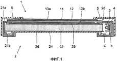
ФИГ.1 представляет собой схематичное сечение, показывающее пример устройства жидкокристаллического дисплея (устройства плоского дисплея) и устройства подсветки. Как показано на ФИГ.1, устройство жидкокристаллического дисплея включает в себя устройство 2 подсветки и жидкокристаллическую панель 1.FIG. 1 is a schematic sectional view showing an example of a liquid crystal display device (flat display device) and a backlight device. As shown in FIG. 1, the liquid crystal display device includes a
В устройстве 2 подсветки нижняя коробчатая рама (рамочный корпус) 21b, открытый на верхней и нижней сторонах, оборудован задним металлическим листом 26 так, чтобы покрыть отверстие с нижней стороны. На заднем металлическом листе 26 оборудована коробчатая пластина световода 22.In the
На обратной поверхности пластины 22 световода оборудован отражающий лист 24; на лицевой поверхности пластины 22 световода, оборудованы три оптических листа 25. На внутренней стенке нижней рамы 21b, которая обращена к боковой поверхности пластины 22 световода, ГПП (гибкая печатная панель) 4 - имеющая множество СИДов (точечных источников света) 3, смонтированных на ней с предварительно определенным интервалом в направлении длины зафиксирована двусторонним адгезивом b, ГПП 4 расположена внутри отражающей кассеты C, имеющей прямоугольное сечение с открытой частью, обращенной на боковую поверхность пластины 22 световода. Структуры СИД 3 и ГПП 4 будут описаны позднее.On the back surface of the
Верхняя рама (рамочный корпус) 21a, имеющая открытую часть, сформированную в ней для того, чтобы пропускать свет, выходящий от пластины 22 световода, установлена так, чтобы покрывать отверстие верхней поверхности нижней рамы 21b; с помощью верхней рамы 21a и нижней рамы 21b, задний металлический лист 26, отражающий лист 24, пластина 22 световода и оптические листы 25 удерживаются вместе.An upper frame (frame body) 21a having an open portion formed therein to transmit light exiting from the
С другой стороны, в жидкокристаллической панели 1, жидкий кристалл (не изображено) герметично закрыт между парой стеклянных подложек 11 и 12, размещенных отдельно и напротив друг друга. Наружная кромочная часть стеклянной подложки 12 вытягивается наружу за стеклянную подложку 11 и, на этой вытянутой части, сформировано большое количество электродных вводов (не изображено), которые прикладывают напряжения к пиксельным электродам, сформированным на поверхности стеклянной подложки 12. На лицевой и обратной поверхностях жидкокристаллической панели 1 оборудованы поляризирующие пластины 13a и 13b соответственно.On the other hand, in the
На ступенчатой части 28, сформированной вокруг края открытой части верхней рамы 21a устройства 2 подсветки, размещена периферийная часть жидкокристаллической панели 1. Оправа 5 покрывает эту периферийную часть жидкокристаллической панели 1; оправа 5 и верхняя и нижняя рамы 21a и 21b скреплены вместе так, что жидкокристаллическая панель 1 и устройство 2 подсветки соединены так, чтобы составлять устройство жидкокристаллического дисплея.On the stepped
ФИГ.2 представляет собой схематичный вид, показывающий структуру СИД 3 как точечного источника света. СИД 3, показанный на ФИГ.2, включает в себя металлический сердечник 31, сформированный из металла, такого как Cu и Al, устройство СИД (полупроводниковое устройство, излучающее свет) 32 закреплено на верхней поверхности металлического сердечника 31 с помощью проводящего адгезива (не изображен), на основе смолы, и пара элетродных вводов 33a и 33b, размещенных на противоположных местах поперек металлического сердечника 31, отдельно от металлического сердечника 31.FIG.2 is a schematic view showing the structure of
Электродный ввод 33a и металлический сердечник 31 соединены с помощью соединительного провода W1; электродный ввод 33b и электрод верхней поверхности (не изображено) устройства СИД 32 соединены с помощью соединительного провода W2. Периферийная часть металлического сердечника 31 и часть пары электродов 33a и 33b спаяны с помощью изоляционной смолы 34. На верхней поверхности металлического сердечника 31, устройство СИД 32 спаяно светопрозрачной смолой 35 в форме купола; здесь светопрозрачная смола 35 в форме купола также функционирует как линза.The
На ФИГ.2 сердечник 31 сформирован только со стороны нижней поверхности СИД 3. Это, тем не менее, не ограничено; сердечник 31 может тянуться ближе боковой поверхности изоляционной смолы 34. Это увеличивает площадь поверхности сердечника 31 и, таким образом, увеличивает площадь, которая может рассеивать тепло. Более того, это является предпочтительным, потому что сердечник 31 тогда размещается не только на стороне нижней поверхности СИД 3, которая, как следствие, является его стороной, более близкой к ГПП 4, но также на испускающей свет стороне СИД, и таким образом, тепло рассеивается как на стороне нижней поверхности, так и на излучающей свет стороне СИД 3.In FIG. 2, the
Как будет описано дальше, в СИД 3, часть пары электродных вводов 33a и 33b нижняя поверхность металлического сердечника 31 выдается наружу и выступает через изоляционную смолу 34.As will be described later, in
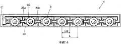
ФИГ.3 представляет собой вид сверху, показывающий пример ГПП 4. ГПП 4 включает в себя гибкую основу 41 ГПП в форме ленты, монтажный проводник 42 и рассеивающий тепло проводник 43, сформированный на поверхности основы 41 ГПП. Следует отметить, что монтажный проводник 42 и рассеивающий тепло проводник 43 отделены друг от друга на предварительно определенный интервал.FIG. 3 is a plan view showing an example of a
В монтажном проводнике 42 сформированы области (заштрихованные прямоугольные части на фигуре), к которым прикреплены электродные вводы каждого СИД; в рассеивающем тепло проводнике 43 сформирована область (заштрихованная круглая часть на фигуре), к которой прикреплен металлический сердечник каждого СИД. Между рассеивающими тепло проводниками 43 и 43, соответственных различных СИДов, сформирован интервал, так, что не было проводимости от одного к другому.In the mounting
Когда СИД 3 установлен на ГПП 4, описанной выше, в области (заштрихованные области на фигуре), к которым прикреплены электродные вводы 33a и 33b и металлический сердечник 31 СИД 3, сразу с помощью трафаретной печати или чего-то похожего наносится проводящий адгезив, такой как припой. Как показано на ФИГ.4 (вид сверху, показывающий ГПП 4 с СИД 3 и соединителем C, смонтированным на нем), СИД 3 смонтирован в предварительно определенном положении на ГПП 4 и закреплен с помощью проводящего адгезива (не изображено). (Следует заметить, что соединитель C установлен к части, к которой подается внешнее питание).When the
Для закрепления электродных вводов 33a и 33b металлического сердечника 31 СИД 3 на ГПП 4, обычно используется два типа адгезива: проводящий адгезив и изоляционный адгезив. Таким образом, требуется два процесса, каждый для нанесения одного адгезива на ГПП. Однако в соответствии с настоящим изобретением может быть использован один и тот же проводящий адгезив; таким образом, адгезив может быть нанесен в одном процессе, повышая тем самым производительность.To fix the
Для повышения эффективности излучения предпочтительно, чтобы слой белой смолы был сформирован на монтажной поверхности ГПП 4. Причина в том, что свет, излучаемый из СИД 3, затем отражается слоем белой смолы для прохождения в пластину 22 световода (показано на ФИГ.1) через его боковую поверхность.To increase the radiation efficiency, it is preferable that a layer of white resin is formed on the mounting surface of the
Тепло, произведенное СИД устройством 32, проходит через металлический сердечник 31 и проводится к рассеивающему тепло проводнику 43 с помощью проводящего адгезива. Как видно из ФИГ.3 и 4, рассеивающие тепло проводники 43 сформированы широко на поверхности ГПП 4. Таким образом, тепло, произведенное СИД устройством 32, рассеивается в воздух из широких рассеивающих тепло проводников 43, эффективно подавляя рост температуры в СИД устройстве 32.The heat generated by the
Как описано выше, с помощью использования одного и того же проводящего адгезива электродные вводы 33a и 33b и металлический сердечник 31 СИД 3 закрепляются на ГПП 4. Таким образом, если рассеивающие тепло проводники 43 различных СИДов 3 находятся в контакте друг с другом, ток проходит сквозь рассеивающие тепло проводники 43 через металлический сердечник 31 и вызывает короткое замыкание. Поэтому необходимо разделить рассеивающие тепло проводники 43 так, чтобы не было проводимости от одного к другому.As described above, by using the same conductive adhesive, the
Хотя нет особых ограничений на то, где разделять различные рассеивающие тепло проводники 43, предпочтительно, чтобы они были разделены посередине (L/2) расстояния L между СИДами, как показано на ФИГ.4.Although there are no particular restrictions on where to separate the various heat-dissipating conductors 43, it is preferable that they are separated in the middle (L / 2) of the distance L between the LEDs, as shown in FIG. 4.
В целом, поскольку ГПП 4 является гибкой, она имеет тенденцию изгибаться особенно в разделительной части, где не сформирован рассеивающий тепло проводник 43. Таким образом, как показано на ФИГ.5A, если разделительная часть между различными рассеивающими тепло проводниками 43 находится близко к СИД 3, ГПП 4 может изгибаться и провисать около СИД 3, вызывая то, что часть, где СИД 3 закреплен с помощью припоя, отойдет от ГПП 4.In general, since the
С другой стороны, как показано на ФИГ.5B, когда разделительная часть между различными рассеивающими тепло проводниками 43 расположена в средней точке между двумя СИДами 3 и 3, изгиб ГПП 4 в разделительной части не повлияет на СИД 3, уменьшая вероятность того, что СИД 3 отойдет от ГПП 4.On the other hand, as shown in FIG. 5B, when the separation part between the various heat dissipating conductors 43 is located at a midpoint between the two
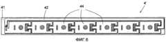
Другой вариант осуществления показан на ФИГ.6. По сравнению с ГПП 4, показанной на ФИГ.3, ГПП 4', показанная на ФИГ.6, отличается тем, что монтажный проводник 42 (показан на ФИГ.3), соединенный с электродным вводом 33a СИД 3, и рассеивающий тепло проводник 43 (показан на ФИГ.3) объединены друг с другом.Another embodiment is shown in FIG. 6. Compared to the
На ГПП 4, показанной на ФИГ.3, монтажный проводник 42, соединенный с электродным вводом 33a СИД 3 и с рассеивающим тепло проводником 43 имеют одинаковый потенциал через металлический сердечник 31. Таким образом, на ГПП 4', показанной на ФИГ.6, монтажный проводник и рассеивающий тепло проводник объединены друг с другом для формирования покрывающего большую площадь рассеивающего тепло проводника 44, который рассеивает большее количество тепла. Следует заметить, что здесь нанесение проводящего адгезива и монтаж СИД 3 и соединителя C происходит в схожем порядке, как и описанном выше варианте осуществления, и поэтому повторяться описание не будет.In the
Касательно проводящего адгезива, кроме припоя или Ag пасты, упомянутых выше, может быть использован любой известный обычный материал. Тем не менее, предпочтительно, чтобы проводящий адгезив имел высокую проводимость тепла, припой является подходящим.Regarding the conductive adhesive, in addition to the solder or Ag paste mentioned above, any known conventional material may be used. However, it is preferable that the conductive adhesive has a high heat conductivity, solder is suitable.
Claims (4)
Translated fromRussianпластину световода и множество точечных источников света, смонтированных на гибкой печатной плате, расположенной рядом с боковой поверхностью пластины световода, в котором точечный источник света содержит полупроводниковое светоизлучающее устройство, металлический сердечник, собранный с полупроводниковым устройством, и электродный ввод, при этом часть металлического сердечника выступает со стороны монтажной поверхности, гибкая печатная плата содержит монтажный проводник, соединенный с электродным вводом точечного источника света и рассевающий тепло проводник, соответствующий точечному источнику света и отделенный от смежного рассеивающего тепло проводника так, чтобы не было проводимости от одного другому, электродный ввод точечного источника света и монтажный проводник гибкой печатной платы скреплены вместе с помощью проводящего адгезива, и металлический сердечник точечного источника света и рассеивающий тепло проводник гибкой печатной платы скреплены вместе с помощью проводящего адгезива.1. The backlight device containing
a light guide plate and a plurality of point light sources mounted on a flexible printed circuit board located near the side surface of the light guide plate, in which the point light source comprises a semiconductor light emitting device, a metal core assembled with a semiconductor device, and an electrode input, while a portion of the metal core protrudes on the mounting surface side, the flexible circuit board contains a mounting conductor connected to the electrode input of a point light source and a heat dissipating conductor corresponding to a point light source and separated from an adjacent heat dissipating conductor so that there is no conductivity from one another, the electrode input of the point light source and the mounting conductor of the flexible printed circuit board are fastened together using a conductive adhesive, and the metal core of the point light source and the heat dissipating conductor of the flexible printed circuit board is fastened together using a conductive adhesive.
Applications Claiming Priority (2)
| Application Number | Priority Date | Filing Date | Title |
|---|---|---|---|
| JP2007035625 | 2007-02-16 | ||
| JP2007-035625 | 2007-02-16 |
Publications (2)
| Publication Number | Publication Date |
|---|---|
| RU2009134481A RU2009134481A (en) | 2011-03-27 |
| RU2419740C1true RU2419740C1 (en) | 2011-05-27 |
Family
ID=39689786
Family Applications (1)
| Application Number | Title | Priority Date | Filing Date |
|---|---|---|---|
| RU2009134481/28ARU2419740C1 (en) | 2007-02-16 | 2007-10-10 | Highlighter and flat display with said highlighter |
Country Status (4)
| Country | Link |
|---|---|
| US (1) | US8157430B2 (en) |
| CN (1) | CN101611262B (en) |
| RU (1) | RU2419740C1 (en) |
| WO (1) | WO2008099531A1 (en) |
Cited By (4)
| Publication number | Priority date | Publication date | Assignee | Title |
|---|---|---|---|---|
| WO2013154452A1 (en)* | 2012-04-13 | 2013-10-17 | Общество с ограниченной ответственностью "ДиС ПЛЮС" | Method for assembling a block of radiation sources and light-emitting diode lighting device comprising such a block |
| RU2633391C2 (en)* | 2011-11-17 | 2017-10-12 | Филипс Лайтинг Холдинг Б.В. | Direct view light based on light emitting diodes (leds) with homogeneous mixing of output light |
| RU191979U1 (en)* | 2018-12-19 | 2019-08-29 | Юрий Борисович Соколов | PCB FOR LIGHTING THE END SURFACE OF THE FIBER GUIDE |
| RU200958U1 (en)* | 2020-07-22 | 2020-11-20 | Станислав Владимирович Степанов | Decorative mirror block |
Families Citing this family (22)
| Publication number | Priority date | Publication date | Assignee | Title |
|---|---|---|---|---|
| KR101545939B1 (en)* | 2008-10-27 | 2015-08-21 | 삼성디스플레이 주식회사 | Light source module, method of manufacturing same, and backlight assembly having same |
| CN102170747B (en)* | 2010-02-26 | 2013-04-03 | 佳必琪国际股份有限公司 | Extrusion type flexible circuit board, its manufacturing method and strip light with the circuit board |
| US8710525B2 (en)* | 2010-03-15 | 2014-04-29 | Nichia Corporation | Light emitting device |
| WO2011125346A1 (en)* | 2010-04-07 | 2011-10-13 | シャープ株式会社 | Light emitting device and method for manufacturing same |
| US8419203B1 (en)* | 2010-09-03 | 2013-04-16 | Rockwell Collins, Inc. | Single card multi mode LCD backlight |
| EP2437581A1 (en)* | 2010-09-30 | 2012-04-04 | Odelo GmbH | Light diode on a ceramic substrate basis |
| JP2012113919A (en)* | 2010-11-24 | 2012-06-14 | Toshiba Corp | Lighting device |
| AU2014200021B2 (en)* | 2010-12-28 | 2015-07-09 | Nichia Corporation | Light emitting device |
| BR112013001195B1 (en)* | 2010-12-28 | 2021-03-02 | Nichia Corporation | light-emitting device and method for making the same |
| DE102011110799A1 (en)* | 2011-08-22 | 2013-02-28 | Heraeus Materials Technology Gmbh & Co. Kg | Substrate for the construction of electronic elements |
| US8851736B2 (en)* | 2011-08-30 | 2014-10-07 | Lg Innotek Co., Ltd. | Light emitting module with heatsink plate having coupling protrusions |
| US20130100694A1 (en)* | 2011-10-24 | 2013-04-25 | Kocam International Co., Ltd. | LED Backlight Module |
| TWI460495B (en)* | 2011-11-07 | 2014-11-11 | Au Optronics Corp | Display module |
| JP5587949B2 (en)* | 2011-11-10 | 2014-09-10 | 京セラコネクタプロダクツ株式会社 | Semiconductor light emitting element mounting module and semiconductor light emitting element module |
| KR102030382B1 (en)* | 2011-11-22 | 2019-10-11 | 삼성디스플레이 주식회사 | Light emitting module, backlight assembly having the same and display apparatus having the same |
| CN102686020A (en)* | 2012-06-11 | 2012-09-19 | 深圳市华星光电技术有限公司 | Printed circuit board of backlight module, backlight module and liquid crystal displayer thereof |
| JP6079159B2 (en) | 2012-11-16 | 2017-02-15 | 日亜化学工業株式会社 | Light emitting device |
| US10257932B2 (en)* | 2016-02-16 | 2019-04-09 | Microsoft Technology Licensing, Llc. | Laser diode chip on printed circuit board |
| JP6941794B2 (en)* | 2017-02-09 | 2021-09-29 | パナソニックIpマネジメント株式会社 | Image display device and component mounting board |
| CN107247364B (en)* | 2017-07-27 | 2021-01-26 | 京东方科技集团股份有限公司 | Backlight module and display device |
| US10852583B2 (en)* | 2018-09-17 | 2020-12-01 | Sharp Kabushiki Kaisha | Lighting device, display device, and method of producing lighting device |
| CN110045541B (en) | 2019-03-28 | 2021-02-26 | 武汉华星光电技术有限公司 | Backlight structure, liquid crystal display panel and electronic equipment |
Citations (5)
| Publication number | Priority date | Publication date | Assignee | Title |
|---|---|---|---|---|
| JP2002368285A (en)* | 2001-06-11 | 2002-12-20 | Omron Corp | Light emitting device, light emitting module and manufacturing method thereof |
| JP2004158275A (en)* | 2002-11-06 | 2004-06-03 | Matsushita Electric Ind Co Ltd | Backlight |
| JP2005353914A (en)* | 2004-06-11 | 2005-12-22 | Toshiba Corp | Semiconductor light emitting device, manufacturing method thereof, and semiconductor light emitting unit |
| JP2006058741A (en)* | 2004-08-23 | 2006-03-02 | Optrex Corp | Liquid crystal display device |
| JP2006310123A (en)* | 2005-04-28 | 2006-11-09 | Minebea Co Ltd | Planar lighting system |
Family Cites Families (14)
| Publication number | Priority date | Publication date | Assignee | Title |
|---|---|---|---|---|
| JP3642263B2 (en)* | 2000-05-23 | 2005-04-27 | セイコーエプソン株式会社 | Liquid crystal device and electronic device |
| JP4737575B2 (en) | 2001-01-30 | 2011-08-03 | ハリソン東芝ライティング株式会社 | Light emitting diode array and light source device |
| JP2005283852A (en) | 2004-03-29 | 2005-10-13 | Kyocera Corp | Liquid crystal display |
| JP2006011239A (en) | 2004-06-29 | 2006-01-12 | Kyocera Corp | Liquid crystal display |
| TWI333576B (en)* | 2005-08-17 | 2010-11-21 | Au Optronics Corp | Bottom lighting module |
| JP4470906B2 (en) | 2006-05-11 | 2010-06-02 | 株式会社デンソー | Lighting device |
| KR100764388B1 (en)* | 2006-03-17 | 2007-10-05 | 삼성전기주식회사 | Anodized Metal Substrate Module |
| KR101294008B1 (en)* | 2006-07-24 | 2013-08-07 | 삼성디스플레이 주식회사 | Backlight assembly, method of manufacturing the same and display device having the same |
| US20080049164A1 (en)* | 2006-08-22 | 2008-02-28 | Samsung Electronics Co., Ltd., | Backlight assembly, manufacturing method thereof, and liquid crystal display device |
| KR100844757B1 (en)* | 2006-08-24 | 2008-07-07 | 엘지이노텍 주식회사 | Light source device and display device using same |
| US20090103295A1 (en)* | 2007-10-17 | 2009-04-23 | Keeper Technology Co., Ltd. | LED unit and LED module |
| KR101535064B1 (en)* | 2008-01-17 | 2015-07-09 | 삼성디스플레이 주식회사 | Light source module for display device and display device including same |
| CN101539278B (en)* | 2008-03-19 | 2010-11-10 | 富准精密工业(深圳)有限公司 | Light-emitting diode assemble |
| CN101645478A (en)* | 2008-08-08 | 2010-02-10 | 鸿富锦精密工业(深圳)有限公司 | Light emitting diode (LED) radiating structure |
- 2007
- 2007-10-10WOPCT/JP2007/069731patent/WO2008099531A1/enactiveApplication Filing
- 2007-10-10USUS12/527,336patent/US8157430B2/ennot_activeExpired - Fee Related
- 2007-10-10RURU2009134481/28Apatent/RU2419740C1/ennot_activeIP Right Cessation
- 2007-10-10CNCN2007800514338Apatent/CN101611262B/ennot_activeExpired - Fee Related
Patent Citations (5)
| Publication number | Priority date | Publication date | Assignee | Title |
|---|---|---|---|---|
| JP2002368285A (en)* | 2001-06-11 | 2002-12-20 | Omron Corp | Light emitting device, light emitting module and manufacturing method thereof |
| JP2004158275A (en)* | 2002-11-06 | 2004-06-03 | Matsushita Electric Ind Co Ltd | Backlight |
| JP2005353914A (en)* | 2004-06-11 | 2005-12-22 | Toshiba Corp | Semiconductor light emitting device, manufacturing method thereof, and semiconductor light emitting unit |
| JP2006058741A (en)* | 2004-08-23 | 2006-03-02 | Optrex Corp | Liquid crystal display device |
| JP2006310123A (en)* | 2005-04-28 | 2006-11-09 | Minebea Co Ltd | Planar lighting system |
Cited By (5)
| Publication number | Priority date | Publication date | Assignee | Title |
|---|---|---|---|---|
| RU2633391C2 (en)* | 2011-11-17 | 2017-10-12 | Филипс Лайтинг Холдинг Б.В. | Direct view light based on light emitting diodes (leds) with homogeneous mixing of output light |
| WO2013154452A1 (en)* | 2012-04-13 | 2013-10-17 | Общество с ограниченной ответственностью "ДиС ПЛЮС" | Method for assembling a block of radiation sources and light-emitting diode lighting device comprising such a block |
| EA025099B1 (en)* | 2012-04-13 | 2016-11-30 | Общество с ограниченной ответственностью "ДиС ПЛЮС" | Method for assembling a block of radiation sources and light-emitting diode lighting device comprising such a block |
| RU191979U1 (en)* | 2018-12-19 | 2019-08-29 | Юрий Борисович Соколов | PCB FOR LIGHTING THE END SURFACE OF THE FIBER GUIDE |
| RU200958U1 (en)* | 2020-07-22 | 2020-11-20 | Станислав Владимирович Степанов | Decorative mirror block |
Also Published As
| Publication number | Publication date |
|---|---|
| US8157430B2 (en) | 2012-04-17 |
| RU2009134481A (en) | 2011-03-27 |
| WO2008099531A1 (en) | 2008-08-21 |
| US20100027291A1 (en) | 2010-02-04 |
| CN101611262A (en) | 2009-12-23 |
| CN101611262B (en) | 2011-01-26 |
Similar Documents
| Publication | Publication Date | Title |
|---|---|---|
| RU2419740C1 (en) | Highlighter and flat display with said highlighter | |
| US8199306B2 (en) | Printed circuit board, backlight unit having the printed circuit board, and liquid crystal display device having the printed circuit board | |
| US7168842B2 (en) | Light emitting diode backlight package | |
| CN103149720B (en) | Liquid crystal indicator | |
| CN101153979B (en) | Backlight assembly and cover for a compact display apparatus | |
| US7667378B2 (en) | Illuminating device, electro-optic device, and electronic apparatus | |
| US20060098441A1 (en) | Backlight module | |
| US8684581B2 (en) | Light-emitting diode package, light source module having the same and backlight assembly having the same | |
| CN105158973A (en) | Liquid crystal display device | |
| KR20090079415A (en) | Light source module for display device and display device including same | |
| US8625053B2 (en) | Light emitting diode and backlight unit and liquid crystal display device with the same | |
| CN101416101A (en) | Liquid crystal display | |
| CN101963336A (en) | Apparatus for radiating heat of light emitting diode and liquid crystal display using the same | |
| CN106154646B (en) | Lamp panel, backlight module and liquid crystal display device | |
| CN100388092C (en) | Heat dissipation structure of backlight module | |
| CN102193245A (en) | Liquid crystal display device | |
| CN101922648A (en) | Backlight module | |
| US8684550B2 (en) | Light source, light-emitting module having the same and backlight unit have the same | |
| US12230228B2 (en) | Light-emitting assembly for enhancing optical performance | |
| CN103728771B (en) | Liquid crystal indicator | |
| JP2008066132A (en) | LIGHT EMITTING DEVICE AND DISPLAY DEVICE USING THE LIGHT EMITTING DEVICE | |
| KR101245086B1 (en) | Backlight unit and liquid crystal display device having thereof | |
| KR20080012511A (en) | LED unit, backlight unit using same, and display device having same | |
| KR20090104521A (en) | Backlight unit | |
| KR102331265B1 (en) | Display device |
Legal Events
| Date | Code | Title | Description |
|---|---|---|---|
| MM4A | The patent is invalid due to non-payment of fees | Effective date:20151011 |