RU2390918C1 - Precision operational amplifier - Google Patents
Precision operational amplifierDownload PDFInfo
- Publication number
- RU2390918C1 RU2390918C1RU2009102889/09ARU2009102889ARU2390918C1RU 2390918 C1RU2390918 C1RU 2390918C1RU 2009102889/09 ARU2009102889/09 ARU 2009102889/09ARU 2009102889 ARU2009102889 ARU 2009102889ARU 2390918 C1RU2390918 C1RU 2390918C1
- Authority
- RU
- Russia
- Prior art keywords
- collector
- input
- output
- emitter
- circuit
- Prior art date
Links
- 230000005855radiationEffects0.000abstractdescription4
- 230000000694effectsEffects0.000abstractdescription2
- 230000003321amplificationEffects0.000abstract1
- 238000003199nucleic acid amplification methodMethods0.000abstract1
- 239000000126substanceSubstances0.000abstract1
- 238000010586diagramMethods0.000description3
- 238000005094computer simulationMethods0.000description2
- 230000009897systematic effectEffects0.000description2
- 230000005540biological transmissionEffects0.000description1
- 238000006243chemical reactionMethods0.000description1
Images


Landscapes
- Amplifiers (AREA)
Abstract
Description
Translated fromRussianИзобретение относится к области радиотехники и связи и может быть использовано в качестве устройства усиления аналоговых сигналов, в структуре аналоговых микросхем различного функционального назначения (например, решающих усилителях с малыми значениями эдс смещения нуля и его дрейфа в условиях воздействия температуры или радиации).The invention relates to the field of radio engineering and communication and can be used as a device for amplifying analog signals in the structure of analog microcircuits of various functional purposes (for example, decision amplifiers with small values of the emf of zero offset and its drift under conditions of temperature or radiation).
В современной радиоэлектронной аппаратуре находят применение операционные усилители (ОУ) с существенными различными параметрами. Особое место занимают ОУ с простейшей архитектурой, содержащие небольшое число элементов. На их основе выполняются, например, различные классы селективных цепей, где число маломощных усилителей может измеряться десятками единиц. Предлагаемое изобретение относится к данному типу устройств.In modern electronic equipment, operational amplifiers (op amps) with significant different parameters are used. A special place is occupied by op amps with the simplest architecture, containing a small number of elements. On their basis, for example, various classes of selective circuits are performed, where the number of low-power amplifiers can be measured in tens of units. The present invention relates to this type of device.
Наиболее близкой по технической сущности к заявляемому ОУ является классическая схема фиг.1 (патент США №4.410.859, fig.1), которая стала основой построения большого числа аналоговых устройств различного назначения, в том числе микросхем (574УД3, 153УД2, 1407УД3, СА3078 и др. [1-13]).The closest in technical essence to the claimed op-amp is the classical circuit of figure 1 (US patent No. 4.410.859, fig.1), which became the basis for constructing a large number of analog devices for various purposes, including microcircuits (574UD3, 153UD2, 1407UD3, CA3078 et al. [1-13]).
Существенные недостатки известного ОУ фиг.1 состоят в том, что он имеет повышенное значение систематической составляющей напряжения смещения нуля Uсм и высокую нестабильность Uсм вследствие воздействия температуры или радиации.Significant disadvantages of the known op-amp of Fig. 1 are that it has an increased value of the systematic component of the bias voltage of zero Ucm and high instability Ucm due to temperature or radiation.
Основная цель предлагаемого изобретения состоит в уменьшении Uсм.The main objective of the invention is to reduce Usee
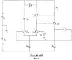
Поставленная цель достигается тем, что в операционном усилителе фиг.1, содержащем входной дифференциальный каскад 1 с первым 2 и вторым 3 коллекторными выходами, токовое зеркало 4, вход которого связан с первым 2 коллекторным выходом входного дифференциального каскада 1, выходной транзистор 5, база которого связана со вторым 3 коллекторным выходом входного дифференциального каскада 1, эмиттер связан с шиной 6 источника питания через первый 7 вспомогательный резистор, а коллектор соединен с цепью нагрузки 8, предусмотрены новые элементы и связи - в схему введены дополнительный транзистор 9 и цепь смещения потенциала 10, причем эмиттер дополнительного транзистора 9 связан с выходом токового зеркала 4, коллектор - подключен ко второму коллекторному выходу 3 входного дифференциального каскада 1, база - соединена с эмиттером выходного транзистора 5, а вход токового зеркала 4 связан с первым 2 коллекторным выходом входного дифференциального каскада 1 через цепь смещения потенциалов 10.This goal is achieved by the fact that in the operational amplifier of figure 1, containing the input
Схема усилителя-прототипа показана на чертеже фиг.1. На чертеже фиг.2 представлена схема заявляемого устройства в соответствии с формулой изобретения.The amplifier circuit of the prototype is shown in the drawing of figure 1. The drawing of figure 2 presents a diagram of the inventive device in accordance with the claims.
На чертеже фиг.3 показана схема ОУ-прототипа в среде компьютерного моделирования PSpice на моделях интегральных транзисторов ФГУП НПП «Пульсар».The drawing of figure 3 shows a diagram of an op-amp prototype in the environment of computer simulation PSpice on models of integrated transistors of FSUE NPP Pulsar.
На чертеже фиг.4 показана схема заявляемого устройства в среде компьютерного моделирования PSpice на моделях интегральных транзисторов ФГУП НПП «Пульсар».The drawing of figure 4 shows a diagram of the inventive device in a computer simulation environment PSpice on models of integrated transistors FSUE NPP "Pulsar".
Прецизионный операционный усилитель фиг.2 содержит входной дифференциальный каскад 1 с первым 2 и вторым 3 коллекторными выходами, токовое зеркало 4, вход которого связан с первым 2 коллекторным выходом входного дифференциального каскада 1, выходной транзистор 5, база которого связана со вторым 3 коллекторным выходом входного дифференциального каскада 1, эмиттер связан с шиной 6 источника питания через первый 7 вспомогательный резистор, а коллектор соединен с цепью нагрузки 8. В схему введены дополнительный транзистор 9 и цепь смещения потенциала 10, причем эмиттер дополнительного транзистора 9 связан с выходом токового зеркала 4, коллектор - подключен ко второму коллекторному выходу 3 входного дифференциального каскада 1, база -соединена с эмиттером выходного транзистора 5, а вход токового зеркала 4 связан с первым 2 коллекторным выходом входного дифференциального каскада 1 через цепь смещения потенциалов 10.The precision operational amplifier of figure 2 contains an input
В качестве токового зеркала рекомендуется использовать повторители тока Вильсона и другие подсхемы, имеющие малую погрешность передачи входного токового сигнала.As a current mirror, it is recommended to use Wilson current repeaters and other subcircuits having a small error in the transmission of the input current signal.
Рассмотрим основные токовые соотношения для схемы фиг.2.Consider the main current relationships for the circuit of figure 2.
Если принять, что ток общей эмиттерной цепи входного дифференциального каскада 1 равен 2I0, то токи выходов 2 и 3If we assume that the current of the common emitter circuit of the input


где Iб.р - ток базы входного n-р-n транзистора ДУ1.where Ibp is the base current of the input n-pn transistor DN1.
Учитывая, что коэффициент передачи по току токового зеркала 4 (например, схемы Вильсона) равен единице (Ki=1), можно найти ток эмиттера (Iэ9) и ток коллектора (Iк9) транзистора 9Given that the current transfer coefficient of the current mirror 4 (for example, Wilson circuit) is equal to unity (Ki = 1), we can find the emitter current (Ie9 ) and the collector current (Ik9 ) of the transistor 9


где Iб.9 - ток базы транзистора 9.where Ib.9 is the base current of the transistor 9.
Следовательно, сумма токов в узле «А»Therefore, the sum of the currents in the node "A"

илиor

где Iб.5 - ток базы транзистора 5.where Ib.5 is the base current of the
Уравнение (6) можно представить в видеEquation (6) can be represented as

где β5≈β9=20-50 - коэффициент усиления по току базы транзисторов 5 и 9.where β5 ≈β9 = 20-50 is the current gain of the base of
Вследствие воздействия радиации β5 и β9 изменяются в несколько раз, однако и в этом случае Ip≈0.Due to the effect of radiation, β5 and β9 change several times, however, even in this case Ip ≈0.
Как следствие, это уменьшает Uсм, так как разностный ток Iр в узле «А» создает Uсм, зависящее от крутизны преобразования входного напряжения uвx ДУ фиг.2 в выходной ток узла «А»As a result, this reduces Ucm , since the differential current Ip in the node “A” creates Ucm , which depends on the steepness of the conversion of the input voltage uin the remote control of FIG. 2 into the output current of the node “A”

где rэ1=rэ2 - сопротивления эмиттерных переходов входных транзисторов дифференциального каскада 1.where re1 = re2 are the resistance of the emitter junctions of the input transistors of the
Поэтому для схем фиг.2Therefore, for the schemes of figure 2

где φт - температурный потенциал.where φt is the temperature potential.
В ДУ-прототипе Ip≠0, поэтому здесь систематическая составляющая Uсм получается на порядок больше (фиг.3, Uсм=1,08 мВ), чем в заявляемой схеме (фиг.4, Uсм=86 мкВ).In the remote control prototype Ip ≠ 0, therefore, the systematic component of Ucm is obtained an order of magnitude greater (Fig. 3, Ucm = 1.08 mV) than in the claimed circuit (Fig. 4, Ucm = 86 μV).
Таким образом, заявляемое устройство имеет существенное преимущество в сравнении с прототипом.Thus, the claimed device has a significant advantage in comparison with the prototype.
Источники информацииInformation sources
1. Патент США №4.410.859, fig.1.1. U.S. Patent No. 4,410.859, fig. 1.
2. Патент США №4.721.920.2. US patent No. 4.721.920.
3. Патент США №4.783.637.3. US patent No. 4.783.637.
4. А.св. СССР №678639.4. A. St. USSR No. 678639.
5. Патент США №4.560.948.5. US Patent No. 4,560,948.
6. А.св. №1193773.6. A. St. No. 1193773.
7. Патент США №4.463.319.7. US patent No. 4.463.319.
8. Патент W003/063344A1.8. Patent W003 / 063344A1.
9. Патент США №5.343.164.9. US patent No. 5.343.164.
10. Патент США №4.417.216.10. US patent No. 4.417.216.
11. Патент США №5.365.191, fig.7.11. US patent No. 5.365.191, fig. 7.
12. Патент США №4.163.90812. US Patent No. 4.163.908
13. Патент Японии №54-37561, fig.1.13. Japanese Patent No. 54-37561, fig. 1.
Claims (1)
Translated fromRussianPriority Applications (1)
| Application Number | Priority Date | Filing Date | Title |
|---|---|---|---|
| RU2009102889/09ARU2390918C1 (en) | 2009-01-29 | 2009-01-29 | Precision operational amplifier |
Applications Claiming Priority (1)
| Application Number | Priority Date | Filing Date | Title |
|---|---|---|---|
| RU2009102889/09ARU2390918C1 (en) | 2009-01-29 | 2009-01-29 | Precision operational amplifier |
Publications (1)
| Publication Number | Publication Date |
|---|---|
| RU2390918C1true RU2390918C1 (en) | 2010-05-27 |
Family
ID=42680617
Family Applications (1)
| Application Number | Title | Priority Date | Filing Date |
|---|---|---|---|
| RU2009102889/09ARU2390918C1 (en) | 2009-01-29 | 2009-01-29 | Precision operational amplifier |
Country Status (1)
| Country | Link |
|---|---|
| RU (1) | RU2390918C1 (en) |
Citations (4)
| Publication number | Priority date | Publication date | Assignee | Title |
|---|---|---|---|---|
| US4410859A (en)* | 1979-02-05 | 1983-10-18 | Tokyo Shibaura Denki Kabushiki Kaisha | Signal amplifier circuit arrangement with output current limiting function |
| US4595883A (en)* | 1983-09-06 | 1986-06-17 | Pioneer Electronic Corporation | Emitter-follower type single-ended push-pull circuit |
| RU2070768C1 (en)* | 1992-06-22 | 1996-12-20 | Научно-исследовательский институт полупроводниковых приборов | Operational amplifier |
| US6114904A (en)* | 1997-10-27 | 2000-09-05 | Sgs-Thomson Microelectronics S.A. | Fast amplifier output stage |
- 2009
- 2009-01-29RURU2009102889/09Apatent/RU2390918C1/ennot_activeIP Right Cessation
Patent Citations (4)
| Publication number | Priority date | Publication date | Assignee | Title |
|---|---|---|---|---|
| US4410859A (en)* | 1979-02-05 | 1983-10-18 | Tokyo Shibaura Denki Kabushiki Kaisha | Signal amplifier circuit arrangement with output current limiting function |
| US4595883A (en)* | 1983-09-06 | 1986-06-17 | Pioneer Electronic Corporation | Emitter-follower type single-ended push-pull circuit |
| RU2070768C1 (en)* | 1992-06-22 | 1996-12-20 | Научно-исследовательский институт полупроводниковых приборов | Operational amplifier |
| US6114904A (en)* | 1997-10-27 | 2000-09-05 | Sgs-Thomson Microelectronics S.A. | Fast amplifier output stage |
Similar Documents
| Publication | Publication Date | Title |
|---|---|---|
| RU2523124C1 (en) | Multi-differential operational amplifier | |
| RU2390916C1 (en) | Precision operational amplifier | |
| RU2390918C1 (en) | Precision operational amplifier | |
| RU2331964C1 (en) | Voltage-to-current converter | |
| RU2446555C2 (en) | Differential operational amplifier | |
| RU2416149C1 (en) | Differential operating amplifier with low zero offset voltage | |
| RU2390921C1 (en) | Operational amplifier with low voltage of zero shift | |
| RU2390914C1 (en) | Cascode differential amplifier with low voltage of zero shift | |
| RU2402151C1 (en) | Cascode differential amplifier | |
| RU2416152C1 (en) | Differential operating amplifier | |
| RU2411636C1 (en) | Cascode differential amplifier with low voltage of zero shift | |
| RU2343626C1 (en) | Current mirror | |
| RU2390912C2 (en) | Cascode differential amplifier | |
| RU2365029C1 (en) | Cascode difference amplifier with low offset voltage | |
| RU2621289C1 (en) | Two-stage differential operational amplifier with higher gain | |
| RU2444119C1 (en) | Precision operational amplifier | |
| RU2402155C1 (en) | Differential amplifier with low voltage of zero shift | |
| RU2411641C1 (en) | Differential operational amplifier with low voltage of zero shift | |
| RU2390915C1 (en) | Precision differential amplifier | |
| RU2408975C1 (en) | Cascode differential amplifier | |
| RU2412531C1 (en) | Differential operating amplifier | |
| RU2412540C1 (en) | Differential operating amplifier | |
| RU2579127C1 (en) | Operational amplifier based broadband converter for converting n-current input signals into voltage | |
| RU2402154C1 (en) | Differential amplifier with low voltage of zero shift | |
| RU2412528C1 (en) | Cascode differential operating amplifier with low zero offset voltage |
Legal Events
| Date | Code | Title | Description |
|---|---|---|---|
| MM4A | The patent is invalid due to non-payment of fees | Effective date:20130130 |