RU2216821C2 - Storage, assembly of storages and process of manufacture of storage - Google Patents
Storage, assembly of storages and process of manufacture of storageDownload PDFInfo
- Publication number
- RU2216821C2 RU2216821C2RU97119733/28ARU97119733ARU2216821C2RU 2216821 C2RU2216821 C2RU 2216821C2RU 97119733/28 ARU97119733/28 ARU 97119733/28ARU 97119733 ARU97119733 ARU 97119733ARU 2216821 C2RU2216821 C2RU 2216821C2
- Authority
- RU
- Russia
- Prior art keywords
- barrier
- storage device
- configuration
- charge
- node
- Prior art date
Links
Images


Classifications
- H—ELECTRICITY
- H01—ELECTRIC ELEMENTS
- H01L—SEMICONDUCTOR DEVICES NOT COVERED BY CLASS H10
- H01L21/00—Processes or apparatus adapted for the manufacture or treatment of semiconductor or solid state devices or of parts thereof
- H01L21/02—Manufacture or treatment of semiconductor devices or of parts thereof
- H01L21/04—Manufacture or treatment of semiconductor devices or of parts thereof the devices having potential barriers, e.g. a PN junction, depletion layer or carrier concentration layer
- H01L21/18—Manufacture or treatment of semiconductor devices or of parts thereof the devices having potential barriers, e.g. a PN junction, depletion layer or carrier concentration layer the devices having semiconductor bodies comprising elements of Group IV of the Periodic Table or AIIIBV compounds with or without impurities, e.g. doping materials
- H01L21/28—Manufacture of electrodes on semiconductor bodies using processes or apparatus not provided for in groups H01L21/20 - H01L21/268
- H01L21/28008—Making conductor-insulator-semiconductor electrodes
- H01L21/28017—Making conductor-insulator-semiconductor electrodes the insulator being formed after the semiconductor body, the semiconductor being silicon
- H01L21/28158—Making the insulator
- H01L21/28167—Making the insulator on single crystalline silicon, e.g. using a liquid, i.e. chemical oxidation
- H01L21/28185—Making the insulator on single crystalline silicon, e.g. using a liquid, i.e. chemical oxidation with a treatment, e.g. annealing, after the formation of the gate insulator and before the formation of the definitive gate conductor
- B—PERFORMING OPERATIONS; TRANSPORTING
- B82—NANOTECHNOLOGY
- B82Y—SPECIFIC USES OR APPLICATIONS OF NANOSTRUCTURES; MEASUREMENT OR ANALYSIS OF NANOSTRUCTURES; MANUFACTURE OR TREATMENT OF NANOSTRUCTURES
- B82Y10/00—Nanotechnology for information processing, storage or transmission, e.g. quantum computing or single electron logic
- G—PHYSICS
- G11—INFORMATION STORAGE
- G11C—STATIC STORES
- G11C13/00—Digital stores characterised by the use of storage elements not covered by groups G11C11/00, G11C23/00, or G11C25/00
- G11C13/0002—Digital stores characterised by the use of storage elements not covered by groups G11C11/00, G11C23/00, or G11C25/00 using resistive RAM [RRAM] elements
- G11C13/0009—RRAM elements whose operation depends upon chemical change
- G11C13/0014—RRAM elements whose operation depends upon chemical change comprising cells based on organic memory material
- G—PHYSICS
- G11—INFORMATION STORAGE
- G11C—STATIC STORES
- G11C13/00—Digital stores characterised by the use of storage elements not covered by groups G11C11/00, G11C23/00, or G11C25/00
- G11C13/02—Digital stores characterised by the use of storage elements not covered by groups G11C11/00, G11C23/00, or G11C25/00 using elements whose operation depends upon chemical change
- H—ELECTRICITY
- H01—ELECTRIC ELEMENTS
- H01L—SEMICONDUCTOR DEVICES NOT COVERED BY CLASS H10
- H01L21/00—Processes or apparatus adapted for the manufacture or treatment of semiconductor or solid state devices or of parts thereof
- H01L21/02—Manufacture or treatment of semiconductor devices or of parts thereof
- H01L21/04—Manufacture or treatment of semiconductor devices or of parts thereof the devices having potential barriers, e.g. a PN junction, depletion layer or carrier concentration layer
- H01L21/18—Manufacture or treatment of semiconductor devices or of parts thereof the devices having potential barriers, e.g. a PN junction, depletion layer or carrier concentration layer the devices having semiconductor bodies comprising elements of Group IV of the Periodic Table or AIIIBV compounds with or without impurities, e.g. doping materials
- H01L21/28—Manufacture of electrodes on semiconductor bodies using processes or apparatus not provided for in groups H01L21/20 - H01L21/268
- H01L21/28008—Making conductor-insulator-semiconductor electrodes
- H01L21/28017—Making conductor-insulator-semiconductor electrodes the insulator being formed after the semiconductor body, the semiconductor being silicon
- H01L21/28158—Making the insulator
- H01L21/28167—Making the insulator on single crystalline silicon, e.g. using a liquid, i.e. chemical oxidation
- H01L21/28194—Making the insulator on single crystalline silicon, e.g. using a liquid, i.e. chemical oxidation by deposition, e.g. evaporation, ALD, CVD, sputtering, laser deposition
- H—ELECTRICITY
- H01—ELECTRIC ELEMENTS
- H01L—SEMICONDUCTOR DEVICES NOT COVERED BY CLASS H10
- H01L21/00—Processes or apparatus adapted for the manufacture or treatment of semiconductor or solid state devices or of parts thereof
- H01L21/02—Manufacture or treatment of semiconductor devices or of parts thereof
- H01L21/04—Manufacture or treatment of semiconductor devices or of parts thereof the devices having potential barriers, e.g. a PN junction, depletion layer or carrier concentration layer
- H01L21/18—Manufacture or treatment of semiconductor devices or of parts thereof the devices having potential barriers, e.g. a PN junction, depletion layer or carrier concentration layer the devices having semiconductor bodies comprising elements of Group IV of the Periodic Table or AIIIBV compounds with or without impurities, e.g. doping materials
- H01L21/28—Manufacture of electrodes on semiconductor bodies using processes or apparatus not provided for in groups H01L21/20 - H01L21/268
- H01L21/28008—Making conductor-insulator-semiconductor electrodes
- H01L21/28017—Making conductor-insulator-semiconductor electrodes the insulator being formed after the semiconductor body, the semiconductor being silicon
- H01L21/28158—Making the insulator
- H01L21/28229—Making the insulator by deposition of a layer, e.g. metal, metal compound or poysilicon, followed by transformation thereof into an insulating layer
- H—ELECTRICITY
- H10—SEMICONDUCTOR DEVICES; ELECTRIC SOLID-STATE DEVICES NOT OTHERWISE PROVIDED FOR
- H10D—INORGANIC ELECTRIC SEMICONDUCTOR DEVICES
- H10D30/00—Field-effect transistors [FET]
- H—ELECTRICITY
- H10—SEMICONDUCTOR DEVICES; ELECTRIC SOLID-STATE DEVICES NOT OTHERWISE PROVIDED FOR
- H10D—INORGANIC ELECTRIC SEMICONDUCTOR DEVICES
- H10D30/00—Field-effect transistors [FET]
- H10D30/60—Insulated-gate field-effect transistors [IGFET]
- H10D30/67—Thin-film transistors [TFT]
- H10D30/6728—Vertical TFTs
- H—ELECTRICITY
- H10—SEMICONDUCTOR DEVICES; ELECTRIC SOLID-STATE DEVICES NOT OTHERWISE PROVIDED FOR
- H10D—INORGANIC ELECTRIC SEMICONDUCTOR DEVICES
- H10D30/00—Field-effect transistors [FET]
- H10D30/60—Insulated-gate field-effect transistors [IGFET]
- H10D30/68—Floating-gate IGFETs
- H10D30/688—Floating-gate IGFETs programmed by two single electrons
- H—ELECTRICITY
- H10—SEMICONDUCTOR DEVICES; ELECTRIC SOLID-STATE DEVICES NOT OTHERWISE PROVIDED FOR
- H10D—INORGANIC ELECTRIC SEMICONDUCTOR DEVICES
- H10D64/00—Electrodes of devices having potential barriers
- H10D64/60—Electrodes characterised by their materials
- H10D64/66—Electrodes having a conductor capacitively coupled to a semiconductor by an insulator, e.g. MIS electrodes
- H10D64/68—Electrodes having a conductor capacitively coupled to a semiconductor by an insulator, e.g. MIS electrodes characterised by the insulator, e.g. by the gate insulator
- H10D64/681—Electrodes having a conductor capacitively coupled to a semiconductor by an insulator, e.g. MIS electrodes characterised by the insulator, e.g. by the gate insulator having a compositional variation, e.g. multilayered
- H—ELECTRICITY
- H10—SEMICONDUCTOR DEVICES; ELECTRIC SOLID-STATE DEVICES NOT OTHERWISE PROVIDED FOR
- H10D—INORGANIC ELECTRIC SEMICONDUCTOR DEVICES
- H10D64/00—Electrodes of devices having potential barriers
- H10D64/60—Electrodes characterised by their materials
- H10D64/66—Electrodes having a conductor capacitively coupled to a semiconductor by an insulator, e.g. MIS electrodes
- H10D64/68—Electrodes having a conductor capacitively coupled to a semiconductor by an insulator, e.g. MIS electrodes characterised by the insulator, e.g. by the gate insulator
- H10D64/691—Electrodes having a conductor capacitively coupled to a semiconductor by an insulator, e.g. MIS electrodes characterised by the insulator, e.g. by the gate insulator comprising metallic compounds, e.g. metal oxides or metal silicates
- H—ELECTRICITY
- H01—ELECTRIC ELEMENTS
- H01L—SEMICONDUCTOR DEVICES NOT COVERED BY CLASS H10
- H01L21/00—Processes or apparatus adapted for the manufacture or treatment of semiconductor or solid state devices or of parts thereof
- H01L21/02—Manufacture or treatment of semiconductor devices or of parts thereof
- H01L21/04—Manufacture or treatment of semiconductor devices or of parts thereof the devices having potential barriers, e.g. a PN junction, depletion layer or carrier concentration layer
- H01L21/18—Manufacture or treatment of semiconductor devices or of parts thereof the devices having potential barriers, e.g. a PN junction, depletion layer or carrier concentration layer the devices having semiconductor bodies comprising elements of Group IV of the Periodic Table or AIIIBV compounds with or without impurities, e.g. doping materials
- H01L21/28—Manufacture of electrodes on semiconductor bodies using processes or apparatus not provided for in groups H01L21/20 - H01L21/268
- H01L21/28008—Making conductor-insulator-semiconductor electrodes
- H01L21/28017—Making conductor-insulator-semiconductor electrodes the insulator being formed after the semiconductor body, the semiconductor being silicon
- H01L21/28158—Making the insulator
- H01L21/28167—Making the insulator on single crystalline silicon, e.g. using a liquid, i.e. chemical oxidation
- H01L21/28211—Making the insulator on single crystalline silicon, e.g. using a liquid, i.e. chemical oxidation in a gaseous ambient using an oxygen or a water vapour, e.g. RTO, possibly through a layer
Landscapes
- Engineering & Computer Science (AREA)
- Physics & Mathematics (AREA)
- Chemical & Material Sciences (AREA)
- Manufacturing & Machinery (AREA)
- Microelectronics & Electronic Packaging (AREA)
- Crystallography & Structural Chemistry (AREA)
- Condensed Matter Physics & Semiconductors (AREA)
- General Physics & Mathematics (AREA)
- Power Engineering (AREA)
- Computer Hardware Design (AREA)
- General Chemical & Material Sciences (AREA)
- Chemical Kinetics & Catalysis (AREA)
- Nanotechnology (AREA)
- Mathematical Physics (AREA)
- Theoretical Computer Science (AREA)
- Semiconductor Memories (AREA)
- Non-Volatile Memory (AREA)
Abstract
Description
Translated fromRussian Область техники, к которой относится изобретение
Настоящее изобретение касается запоминающего устройства, способного к интеграции очень высокой степени для обеспечения матрицы ячеек памяти.FIELD OF THE INVENTION
The present invention relates to a storage device capable of integrating a very high degree to provide a matrix of memory cells.
Предпосылки создания изобретения
В традиционных полупроводниковых запоминающих устройствах один бит информации представляется электронами, хранящимися в статическом конденсаторе в каждой ячейке памяти. Двоичное число "1" представляется дефицитом N электронов, а "0" представляется состоянием нейтрального заряда. В обычном 16-мегабитовом динамическом запоминающем устройстве с произвольной выборкой (ДЗУПВ) количество электронов N составляет порядка 800000. Для увеличения объема памяти отдельные ячейки памяти необходимо делать меньше, но этого нельзя достичь просто с помощью уменьшения обычной ячейки памяти, поскольку существует нижний предел для величины N. Количество электронов N ограничивается необходимостью согласовывать ток утечки из ячейки, внутренний шум и влияние падающих альфа-частиц, и эти факторы не снижаются соразмерно с уменьшением площади ячейки памяти. Можно оценить, что N должно быть свыше 130000 в 16-гигабитном ДЗУПВ, то есть коэффициент приблизительно в 6 раз меньше, чем для 16-мегабитного ДЗУПВ. Однако размер ячейки, требуемой для 16-гигабитного ДЗУПВ, необходимо снизить на три порядка по величине по сравнению с 16-мегабитным ДЗУПВ и, следовательно, уменьшенный размер ячейки не может вместить количество электронов, требуемое для удовлетворительной работы. Пытаясь сохранить величину N достаточно большой, исследовали трехмерные конденсаторы с имеющими вырезы или многоуровневыми структурами вместе с пленками конденсаторов, имеющими высокую диэлектрическую проницаемость, но полученные в результате предлагаемые структуры и процессы изготовления оказались крайне сложными. Кроме того, существенно возросло потребление энергии, поскольку во время хранения данных необходимо обновлять сравнительно большое количество N электронов в ячейках, и это время имеет тенденцию сокращаться, так как масштаб устройства минимизируется.BACKGROUND OF THE INVENTION
In traditional semiconductor memory devices, one bit of information is represented by electrons stored in a static capacitor in each memory cell. The binary number "1" appears to be a deficit of N electrons, and "0" appears to be a state of neutral charge. In a conventional 16-megabyte random-access dynamic memory (DRAM), the number of electrons N is of the order of 800,000. To increase the amount of memory, individual memory cells need to be made smaller, but this cannot be achieved simply by reducing the usual memory cell, since there is a lower limit for N. The number of electrons N is limited by the need to coordinate the leakage current from the cell, internal noise, and the influence of incident alpha particles, and these factors do not decrease in proportion to the decrease in area di memories. It can be estimated that N should be over 130,000 in a 16-gigabyte DZUPV, that is, the coefficient is approximately 6 times less than for a 16-megabyte DZUPV. However, the cell size required for the 16-gigabyte DZUPV must be reduced by three orders of magnitude in comparison with the 16-megabit DZUPV and, therefore, the reduced cell size cannot accommodate the number of electrons required for satisfactory operation. Trying to keep the N value large enough, we investigated three-dimensional capacitors with cutouts or multi-level structures along with capacitor films having high dielectric constant, but the resulting proposed structures and manufacturing processes turned out to be extremely complicated. In addition, energy consumption has increased significantly, since during the storage of data it is necessary to update a relatively large number of N electrons in the cells, and this time tends to decrease, since the scale of the device is minimized.
Другой тип запоминающего устройства, который демонстрирует энергонезависимые характеристики, известен как флэш-память. В таком устройстве приблизительно 105 электронов инжектируются в плавающий затвор через туннельный переход, обычно образованный из SiO2 с толщиной порядка 10 нм. Хранящийся заряд образует поле, которое влияет на электрический ток на участке между стоком и истоком. Заряд либо записывается на плавающий затвор, либо стирается с него, применяя электрическое поле через затвор. Во время циклов стирания и записи применяется очень высокое электрическое поле, и в результате пленка SiO2 разрушается, ограничивая срок службы запоминающего устройства заранее определенным количеством циклом стирания-записи, обычно равным порядка 105 циклов. Более того, время стирания-записи обычно составляет несколько миллисекунд, на четыре порядка по величине ниже, чем у обычного ДЗУПВ. Такая плохая характеристика ограничивает применение устройств флэш-памяти.Another type of storage device that exhibits non-volatile characteristics is known as flash memory. In such a device, approximately 105 electrons are injected into the floating gate through a tunnel junction, typically formed of SiO2 with a thickness of about 10 nm. The stored charge forms a field that affects the electric current in the area between the drain and the source. The charge is either recorded on a floating shutter or erased from it by applying an electric field through the shutter. During the erase and write cycles, a very high electric field is applied, and as a result, the SiO2 film is destroyed, limiting the life of the storage device to a predetermined number of erase-write cycles, usually of the order of 105 cycles. Moreover, the erase-recording time is usually several milliseconds, four orders of magnitude lower than that of a conventional RAM. This poor performance limits the use of flash memory devices.
До настоящего времени предлагались альтернативные способы с целью обеспечения запоминающих устройств, которые работают с небольшими, точными количествами электронов, известных как одноэлектронные запоминающие устройства. Одноэлектронное запоминающее устройство описано в заявке этого же заявителя на патент РСТ/GВ93/02581 WO-A-94/15340). Точное количество электронов поступает в узел памяти или покидает его через многотуннельный переход под управлением прикладываемых напряжений затвора, а электронное состояние в узле памяти определяется с помощью электрометра. Однако недостаток устройства заключается в том, что для каждого узла памяти требуется значительное количество схем, и устройство в настоящее время работает только при низкой температуре, ниже температуры жидкого гелия 4,2 К. К. Яно, Т. Ишии, Т. Хашимото, Т. Кобаяси, Ф. Мурай и К. Секи в работе "Транзакции по электронным устройствам", Институт инженеров по электротехнике и радиоэлектронике (IEEE), сентябрь 1994 г. , т.41, 9, стр.1628-1638, и К. Яно, Т. Ишии, Т. Сано, Т. Майн, Ф. Мурай и К. Секи в 1996 г. в работе "Международная конференция по вопросам твердотельных схем". Институт инженеров по электротехнике и радиоэлектронике (IEEE), 1996 г., FR 16.4, стр.266, предложили и продемонстрировали другое одноэлектронное запоминающее устройство. В устройстве используется поликристаллическая пленка, проходящая между истоком и стоком, к которой прикладывается напряжение затвора. Небольшое количество электронов хранится в зернистой структуре поликристаллической кремниевой пленки. Размер памяти является относительно небольшим по сравнению со структурой в упомянутой выше заявке на патент РСТ/GВ93/02581, и она способна работать при комнатной температуре. Кроме того, память демонстрирует несколько преимуществ по сравнению с обычной флэш-памятью, при меньшем времени стирания-записи из-за небольшого количества хранящихся электронов, и оперативный срок службы улучшен благодаря тому, что используется низковольтная туннельная инжекция, а не инжекция электронов высоким полем. Однако время считывания хранящейся информации относительно длительное, порядка нескольких микросекунд, поскольку необходимо иметь достаточно высокое сопротивление между истоком и стоком для гарантии длительного времени хранения электронов в гранулах. To date, alternative methods have been proposed to provide storage devices that work with small, accurate amounts of electrons, known as single-electron storage devices. Single-electron storage device is described in the application of the same applicant for patent PCT / GV93 / 02581 WO-A-94/15340). The exact number of electrons enters or leaves the memory node through a multi-tunnel junction under the control of applied gate voltages, and the electronic state in the memory node is determined using an electrometer. However, the disadvantage of the device is that a significant number of circuits are required for each memory node, and the device currently operates only at a low temperature, below the temperature of liquid helium 4.2 K. K. Yano, T. Ishii, T. Hashimoto, T Kobayashi, F. Murai and K. Seki in "Transactions on Electronic Devices", Institute of Electrical and Electronics Engineers (IEEE), September 1994, Vol. 41, 9, pp. 1628-1638, and K. Yano , T. Ishii, T. Sano, T. Mine, F. Murai and K. Seki in 1996 at the International Conference on Solid State Circuits. The Institute of Electrical and Electronics Engineers (IEEE), 1996, FR 16.4, p. 266, proposed and demonstrated another single-electron storage device. The device uses a polycrystalline film passing between the source and drain, to which the gate voltage is applied. A small number of electrons are stored in the granular structure of a polycrystalline silicon film. The memory size is relatively small compared with the structure in the aforementioned patent application PCT / GB93 / 02581, and it is able to operate at room temperature. In addition, the memory offers several advantages over conventional flash memory, with shorter write-erase times due to the small number of stored electrons, and the operational life is improved due to the use of low-voltage tunnel injection rather than high-field electron injection. However, the reading time of the stored information is relatively long, of the order of several microseconds, since it is necessary to have a sufficiently high resistance between the source and the drain to guarantee a long storage time of electrons in granules.
Другая конструкция описана С. Тивари, Ф. Рэнэ, Х. Хэнэфи, А. Харстейном, Е. Ф. Краббом и К. Ченом в "Журнале прикладной физики", 4 марта 1996 г., том 68, 10, стр. 1377-1379, С. Тивари, Ф. Рэнэ, К. Ченом, Л. Ши и Х. Хэнэфи в "Журнале прикладной физики", 26 августа 1996 г., том 69, 9, стр.1232-1234, и Х.Ай. Хэнэфи, С. Тивари и Ай. Кэном в работе "Транзакции по электронным устройствам". Институт инженеров по электротехнике и радиоэлектронике (IEEE), 9 сентября 1996 г. , т.43, 9, стр.1553-1558. В этом запоминающем устройстве используются кремниевые кристаллы, которые лежат под затвором транзисторного устройства. Электроны инжектируются в кремниевые нанокристаллы, которые имеют размер 5 нм, из кремниевой подложки через тонкий туннельный оксидный слой толщиной порядка 1,1-1,8 нм. Хранящиеся электроны смещают пороговое напряжение транзистора. Время считывания хранящейся информации является сравнительно коротким, порядка нескольких десятков наносекунд, поскольку канал транзистора имеет высокую подвижность электронов. Цикл долговечности для записи и считывания информации существенно улучшен по сравнению с обычным устройством флэш-памяти. Однако время считывания неудовлетворительно большое, порядка нескольких миллисекунд, так как выравнивание зоны проводимости неблагоприятно для туннелирования электронов из нанокристаллов в объемный кремний. Another construction is described by S. Tiwari, F. Rene, H. Hanafi, A. Harstein, E. F. Crabb, and C. Chen in The Journal of Applied Physics, March 4, 1996, vol. 68, 10, p. 1377- 1379, S. Tiwari, F. Rene, C. Chen, L. Shi, and H. Hanafi in the Journal of Applied Physics, August 26, 1996, Vol. 69, 9, pp. 1232-1234, and H. Ay. Hanafi, S. Tiwari and Ay. Ken in his Transaction on Electronic Devices. Institute of Electrical and Electronics Engineers (IEEE), September 9, 1996, Vol. 43, 9, pp. 1553-1558. This storage device uses silicon crystals that lie under the gate of the transistor device. Electrons are injected into silicon nanocrystals, which have a size of 5 nm, from a silicon substrate through a thin tunneling oxide layer with a thickness of the order of 1.1-1.8 nm. The stored electrons bias the threshold voltage of the transistor. The reading time of the stored information is relatively short, of the order of several tens of nanoseconds, since the transistor channel has a high electron mobility. The longevity cycle for writing and reading information is significantly improved compared to a conventional flash memory device. However, the read time is unsatisfactorily large, of the order of several milliseconds, since the alignment of the conduction band is unfavorable for the tunneling of electrons from nanocrystals into bulk silicon.
Другое запоминающее устройство, которое функционирует в соответствии с принципами флэш-памяти, раскрыто в работе "Электрически перепрограммируемая память, использующая структуру двойного инжектора электронов" Д.Дж. Ди-Мария, К.М. Де-Мейера и Д.У. Донга, "Журнал по электронным устройствам". Институт инженеров по электротехнике и радиоэлектронике (IEEE), том EDL-1, 9, сентябрь 1980 г., стр.179-181. В этом устройстве проводимость участка между стоком и истоком управляется зарядом, записываемым или стираемым с плавающего затвора через туннельный переход с электрода затвора. Однако недостатки данного устройства заключаются в том, что оно имеет медленное время считывания-записи, порядка миллисекунд, и что срок службы туннельного перехода ограничен, поскольку, как и в обычной флэш-памяти, используется инжекция высокого поля Фоулера-Нордхейма. Аналогичное устройство описано в патенте США 3878549, выданном С. Ямазаки. Another memory device that operates in accordance with the principles of flash memory is disclosed in the work "Electrically reprogrammable memory using the structure of a double electron injector" D.J. Di Maria, K.M. De Meyer and D.U. Donga, The Journal of Electronic Devices. Institute of Electrical and Electronics Engineers (IEEE), Volume EDL-1, 9, September 1980, pp. 179-181. In this device, the conductivity of the section between the drain and the source is controlled by the charge recorded or erased from the floating gate through the tunnel junction from the gate electrode. However, the disadvantages of this device are that it has a slow read-write time, of the order of milliseconds, and that the tunnel junction life is limited, since, like in conventional flash memory, high-Fowler-Nordheim injection is used. A similar device is described in US Pat. No. 3,878,549 to S. Yamazaki.
Краткое изложение сущности изобретения
С целью преодоления этих проблем и недостатков изобретение обеспечивает запоминающее устройство, содержащее канал для носителей заряда, узел для хранения заряда с целью образования поля, которое изменяет проводимость канала, и конфигурацию туннельного перехода, через который носители заряда туннелируют в ответ на данное напряжение, чтобы запоминаться в узле, где конфигурация туннельного перехода проявляет профиль энергетической зоны, который содержит относительно широкий с точки зрения размера элемент барьера со сравнительно низкой высотой барьера и по меньшей мере один относительно узкий с точки зрения размера элемент барьера со сравнительно большой высотой барьера.Summary of the invention
In order to overcome these problems and disadvantages, the invention provides a storage device comprising a channel for charge carriers, a node for storing a charge to form a field that changes the channel conductivity, and a configuration of a tunnel junction through which charge carriers tunnel in response to a given voltage to be remembered at the node where the configuration of the tunnel junction shows a profile of the energy zone, which contains a relatively wide in terms of size barrier element with a relatively low the height of the barrier and at least one relatively narrow in terms of size barrier element with a relatively large height of the barrier.
Изобретение позволяет оптимизировать для запоминающего устройства время записи, считывания и стирания. The invention allows to optimize the storage time of the recording, reading and erasing.
Относительно широкий элемент барьера профиля энергетической зоны действует как барьер для долгосрочного хранения заряда в узле. Широкий элемент барьера можно повысить и понизить по выбору так, что заряд после этого может туннелировать через относительно узкий элемент барьера, чтобы быть записанным или стертым из узла. A relatively wide element of the energy profile profile barrier acts as a barrier for long-term storage of charge in a site. The wide barrier element can be raised and lowered optionally so that the charge can then tunnel through the relatively narrow barrier element to be recorded or erased from the assembly.
Элемент профиля энергетической зоны, который имеет относительно большую высоту барьера, может быть обеспечен с помощью элемента с шириной 3 нм или меньше. Можно включить множество элементов относительно высокого барьера и можно подходящим образом обеспечить конфигурацию многотуннельного перехода. An energy zone profile element that has a relatively large barrier height can be provided with an element with a width of 3 nm or less. Many elements of a relatively high barrier can be included, and a multi-tunnel junction configuration can be suitably provided.
Конфигурацию барьера можно делать с помощью ряда различных способов. Она может включать чередующиеся слои относительно электропроводного и электроизоляционного материала, где слои совместно обеспечивают относительно широкий элемент барьера небольшой высоты профиля энергетической зоны, а отдельные электроизоляционные слои обеспечивают элементы относительно высокого барьера. Чередующиеся слои могут содержать поликристаллический кремний и нитрид кремния, соответственно, хотя можно использовать и другие материалы. The configuration of the barrier can be done using a number of different methods. It may include alternating layers with respect to the electrically conductive and electrical insulating material, where the layers together provide a relatively wide barrier element with a small height profile of the energy zone, and individual electrical insulating layers provide elements with a relatively high barrier. Alternating layers may contain polycrystalline silicon and silicon nitride, respectively, although other materials may be used.
В качестве альтернативы, конфигурация барьера может содержать конфигурацию барьера Шотки с чередующимися слоями электропроводного материала и полупроводникового материала. Alternatively, the barrier configuration may comprise a Schottky barrier configuration with alternating layers of electrically conductive material and semiconductor material.
Узел хранения заряда может содержать слой электропроводного материала между барьерной конфигурацией и каналом. Узел может содержать множество электропроводных островков. В альтернативном устройстве островки распределены в барьерной конфигурации и могут давать повышение элементам относительно низкого барьера профиля энергетической зоны благодаря их энергии заряда. Островки могут иметь диаметр 5 нм или меньше. Их можно размещать в слоях, разделенных электроизоляционным материалом. The charge storage unit may comprise a layer of electrically conductive material between the barrier configuration and the channel. The site may contain many electrically conductive islands. In an alternative arrangement, the islands are distributed in the barrier configuration and can increase the elements of the relatively low barrier profile of the energy zone due to their charge energy. The islands may have a diameter of 5 nm or less. They can be placed in layers separated by insulating material.
Островки можно образовывать с помощью ряда способов. Они могут содержать нанокристаллы полупроводникового материала. В качестве альтернативы, их можно образовывать из металла, например, с помощью напыления, так, чтобы распределить их в электроизоляционном металлическом окисле. В качестве альтернативы, островки могут содержать частицы, осажденные из жидкой суспензии металлических или полупроводниковых частиц. Islands can be formed using a number of methods. They may contain nanocrystals of a semiconductor material. Alternatively, they can be formed from metal, for example, by sputtering, so as to distribute them in an insulating metal oxide. Alternatively, the islands may contain particles deposited from a liquid suspension of metal or semiconductor particles.
Конфигурацию туннельного перехода можно располагать между каналом и управляющим электродом так, чтобы с помощью изменения напряжения на управляющем электроде можно было управлять величиной заряда, который туннелирует в узел хранения заряда. В другой соответствующей изобретению конфигурации предусмотрен электрод затвора для приложения дополнительного поля к конфигурации барьера заряда для управления туннелированием заряда в узел. The configuration of the tunnel junction can be located between the channel and the control electrode so that by changing the voltage on the control electrode, it is possible to control the amount of charge that tunnels to the charge storage unit. In another configuration according to the invention, a gate electrode is provided for applying an additional field to the configuration of the charge barrier to control charge tunneling into the assembly.
Величина заряда, который может храниться в узле, может ограничиваться посредством эффекта блокировки Кулона, дискретным числом электронов. The amount of charge that can be stored in the site can be limited by the Coulomb blocking effect to a discrete number of electrons.
При использовании конфигурация туннельного перехода демонстрирует диапазон запирающих напряжений, в котором носитель заряда, туннелирующий в узел, блокируется, и может быть обеспечено средство управления для увеличения и уменьшения диапазона запирающих напряжений с целью управления величиной заряда, хранящегося в узле. Величина заряда, которая может храниться в узле, может быть ограничена множеством дискретных электронных состояний. Средство управления может действовать с целью повышения и понижения диапазона запирающих напряжений таким образом, чтобы обеспечить возможность проявлять только выбранное одно из состояний в узле. In use, the tunnel junction configuration demonstrates a blocking voltage range in which the charge carrier tunneling into the node is blocked, and control means can be provided to increase and decrease the blocking voltage range in order to control the amount of charge stored in the node. The amount of charge that can be stored in the site can be limited by many discrete electronic states. The control means can act to increase and decrease the range of blocking voltages in such a way as to provide the ability to manifest only the selected one of the conditions in the node.
В качестве альтернативы, средство управления может функционировать для изменения ширины диапазона запирающих напряжений. Alternatively, the control means may function to vary the width of the blocking voltage range.
Соответствующее изобретению запоминающее устройство пригодно для изготовления в виде множества ячеек памяти в матрице из рядов и столбцов на общей подложке. The storage device according to the invention is suitable for manufacturing as a plurality of memory cells in a matrix of rows and columns on a common substrate.
Данные можно избирательно считывать из каждой ячейки отдельно, а новые данные можно записывать в ячейку или можно обновлять записанные данные. Матрица ячеек памяти может включать линии считывания для обнаружения тока, протекающего по каналам соответствующих столбцов ячеек памяти, линии слов, линии данных для управления барьерными конфигурациями ячеек памяти их соответствующих столбцов, схему предварительной зарядки, предназначенную для предварительной зарядки линии считывания, линии считывания, снимающие уровень заряда в зависимости от хранящегося заряда в узле хранения заряда конкретной одной из ячеек в ее столбце, считываемом под действием напряжения считывания, прикладываемого к соответственной линии слов, схему считывания-записи для передачи уровня напряжения линии считывания в соответствующую линию слов для столбца, выдачу данных в ответ на уровень напряжения в линии данных для обеспечения выходных данных, соответствующих хранящимся данным в ячейке считывания, и средство обновления данных для приложения напряжения записи к линии слов считываемой ячейки так, что данные, соответствующие уровню напряжения в линии данных, записываются обратно в считанную прежде ячейку. Эта матрица также может включать средство для изменения уровня напряжения на линии данных после действия схемы считывания-записи под действием входных данных, подлежащих записи в ячейку, таким образом, что входные данные записываются в ячейку. Data can be selectively read from each cell separately, and new data can be written to the cell or the recorded data can be updated. The matrix of memory cells may include read lines for detecting the current flowing through the channels of the corresponding columns of memory cells, word lines, data lines for controlling the barrier configurations of memory cells of their respective columns, a precharge circuit for precharging the read line, read lines that remove the level charge depending on the stored charge in the charge storage unit of a particular one of the cells in its column, read under the action of the read voltage, the butt referred to the corresponding word line, a read-write circuit for transmitting the voltage level of the read line to the corresponding word line for the column, outputting data in response to the voltage level in the data line to provide output data corresponding to the stored data in the read cell, and data updating means for applying the write voltage to the word line of the cell to be read so that the data corresponding to the voltage level in the data line is written back to the cell previously read. This matrix may also include means for changing the voltage level on the data line after the read-write circuit is activated by the input data to be written to the cell, so that the input data is written to the cell.
Предпочтительные схемы для матрицы можно образовывать на общей подложке с ячейками памяти, а исток и стоки транзисторов в периферийных схемах можно делать с помощью тех же самых этапов процесса, которые используются для образования областей стоков и истоков в ячейках матрицы. Preferred circuits for the matrix can be formed on a common substrate with memory cells, and the source and drains of transistors in peripheral circuits can be done using the same process steps that are used to form the drain and source regions in the matrix cells.
Изобретение также включает способ изготовления запоминающего устройства, которое содержит канал для носителей заряда, узел для хранения заряда, который меняет проводимость канала, и конфигурацию туннельного перехода, через которую носители заряда туннелируют в ответ на данное напряжение, так, чтобы запоминаться в узле, причем способ включает образование конфигурации туннельного перехода таким образом, что она демонстрирует профиль энергетической зоны, который содержит относительно широкий по размеру барьерный компонент с относительно низкой высотой барьера и по меньшей мере один относительно узкий по размеру барьерный компонент с относительно большой высотой барьера. The invention also includes a method of manufacturing a storage device that comprises a channel for charge carriers, a charge storage unit that changes the channel conductivity, and a tunnel junction configuration through which charge carriers tunnel in response to a given voltage so as to be stored in a node, the method includes the configuration of the tunnel junction in such a way that it demonstrates the profile of the energy zone, which contains a relatively wide in size barrier component with a relative but a low barrier height and at least one relatively narrow size barrier component with a relatively large barrier height.
Краткое описание чертежей
Для того чтобы изобретение стало более понятным, теперь в качестве примера будут описаны его варианты осуществления со ссылкой на прилагаемые чертежи, на которых;
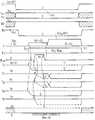
Фиг. 1 представляет схематическое изображение первого типа соответствующего изобретению запоминающего устройства.Brief Description of the Drawings
In order to make the invention more understandable, its embodiments will now be described as an example with reference to the accompanying drawings, in which;
FIG. 1 is a schematic illustration of a first type of storage device according to the invention.
Фиг. 2 представляет график вольт-амперных характеристик показанной на фиг.1 барьерной структуры 2. FIG. 2 is a graph of the current-voltage characteristics of the
Фиг. 3 представляет схематическое изображение принципиальной электрической схемы матрицы из показанных на фиг.1 запоминающих устройств. FIG. 3 is a schematic diagram of a circuit diagram of a matrix of the storage devices shown in FIG. 1.
Фиг.4 представляет схематический вид сверху структурной конфигурации показанной на фиг.3 схемы матрицы памяти. Figure 4 is a schematic top view of the structural configuration of the memory matrix circuit shown in Figure 3.
Фиг. 5 представляет вид в разрезе, взятый по линии А-А' фиг.4 через ячейку памяти M11.FIG. 5 is a sectional view taken along line A-A 'of FIG. 4 through memory cell M11 .
Фиг.6 представляет сечение ячейки М11 фиг.4, взятое по линии В-В'.FIG. 6 is a sectional view of the cell M11 of FIG. 4 taken along line BB '.
Фиг. 7 иллюстрирует способ считывания и записи данных в отдельную ячейку матрицы памяти. FIG. 7 illustrates a method for reading and writing data to a separate cell in a memory matrix.
Фиг. 8 представляет график напряжения V узла памяти 1 запоминающего устройства, построенный относительно напряжения VSY, на истоке и стоке устройства во время записи двоичного "0" (фиг.8а-8d) и записи двоичной "1" (фиг.8е-8h).FIG. 8 is a graph of the voltage V of the
Фиг. 9 представляет график зависимости тока стока-истока ISY от управляющего напряжения затвора VX для двоичной "1" и "0", хранящихся в узле памяти 1.FIG. 9 is a graph of the dependence of the drain-source current ISY on the gate control voltage VX for the binary “1” and “0” stored in the
Фиг. 10 представляет более подробный вид в разрезе барьерной структуры 2 запоминающего устройства. FIG. 10 is a more detailed sectional view of a
Фиг. 11а иллюстрирует диаграмму энергетической зоны проводимости для барьерной структуры 2, при запоминании носителей заряда в узле памяти 1. FIG. 11a illustrates a diagram of the energy conduction band for the
Фиг. 11b иллюстрирует соответствующую диаграмму энергетической зоны, когда носители заряда записываются в узел 1 путем туннелирования из управляющего электрода X. FIG. 11b illustrates the corresponding diagram of the energy zone when charge carriers are recorded in the
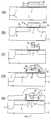
Фиг. 12а-12f представляют виды в поперечном разрезе, соответствующем линии А-А' на фиг. 4, иллюстрирующие различные производственные этапы изготовления запоминающего устройства. FIG. 12a-12f are cross-sectional views corresponding to line A-A 'in FIG. 4 illustrating various manufacturing steps for manufacturing a storage device.
Фиг. 13 представляет схематический поперечный разрез структуры барьера Шотки, который в качестве альтернативы можно использовать в запоминающем устройстве. FIG. 13 is a schematic cross-sectional view of a structure of a Schottky barrier that can alternatively be used in a storage device.
Фиг.14 представляет схематический поперечный разрез альтернативной барьерной структуры, которая включает проводящие островки нанометрического масштаба, для третьего варианта осуществления запоминающего устройства в соответствии с изобретением. FIG. 14 is a schematic cross-sectional view of an alternative barrier structure that includes nanometer-scale conductive islands for a third embodiment of a storage device in accordance with the invention.
Фиг. 15 иллюстрирует ряд производственных этапов для изготовления соответствующего изобретению запоминающего устройства, в котором кремниевые кристаллы нанометрического масштаба распределены по всему SiO2.FIG. 15 illustrates a series of manufacturing steps for manufacturing a storage device according to the invention in which nanometer-scale silicon crystals are distributed throughout SiO2 .
Фиг. 16а-16f иллюстрируют этапы процесса для образования альтернативного варианта осуществления, в котором барьерная структура включает золотые частицы нанометрического масштаба, осаждаемые из коллоидного раствора. FIG. 16a-16f illustrate process steps for forming an alternative embodiment in which the barrier structure includes nanometer-sized gold particles deposited from a colloidal solution.
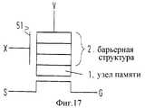
Фиг. 17 представляет схематическое изображение второго типа соответствующего изобретению запоминающего устройства. FIG. 17 is a schematic illustration of a second type of storage device according to the invention.
Фиг. 18а и 18b представляют графики тока I, протекающего через барьерную структуру 2 фиг. 17, в функции напряжения VY, прикладываемого к контакту Y при наличии (режим "включено") напряжения, приложенного к контакту X, и при отсутствии такого напряжения (режим "выключено").FIG. 18a and 18b are graphs of current I flowing through the
Фиг. 19 представляет увеличенное схематическое поперечное сечение показанной на фиг.17 барьерной структуры. FIG. 19 is an enlarged schematic cross-section of the barrier structure shown in FIG.
Фиг.20 представляет диаграмму энергий в зоне проводимости для показанной на фиг.19 барьерной структуры. Fig.20 is a diagram of the energies in the conduction band for the barrier structure shown in Fig.19.
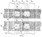
Фиг.21 представляет схематический вид сверху матрицы ячеек памяти, включающей запоминающие устройства показанного на фиг.17 второго типа. Fig.21 is a schematic top view of a matrix of memory cells including storage devices shown in Fig.17 of the second type.
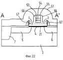
Фиг. 22 представляет вид в поперечном разрезе, взятый по линии А-А' фиг. 21. FIG. 22 is a cross-sectional view taken along line A-A 'of FIG. 21.
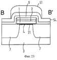
Фиг. 23 представляет вид в поперечном разрезе, взятый по линии В-В' фиг. 21. FIG. 23 is a cross-sectional view taken along line BB 'of FIG. 21.
Фиг. 24 представляет электрическую принципиальную схему показанной на фиг. 21, 22 и 23 конфигурации ячейки памяти совместно со встроенными драйверами и другими периферийными устройствами. FIG. 24 is an electrical circuit diagram shown in FIG. 21, 22, and 23 memory cell configurations with integrated drivers and other peripherals.
Фиг. 25 представляет диаграмму формы сигнала, иллюстрирующую процесс считывания информации из ячейки памяти M11.FIG. 25 is a waveform diagram illustrating a process of reading information from a memory cell M11 .
Фиг. 26 представляет диаграмму формы сигнала, иллюстрирующую процесс записи данных в ячейку памяти М11.FIG. 26 is a waveform diagram illustrating a process of writing data to a memory cell M11 .
Фиг.27а-27е иллюстрируют этапы обработки для изготовления показанного на фиг.21-23 запоминающего устройства. FIGS. 27a – 27e illustrate processing steps for manufacturing the storage device shown in FIGS. 21-23.
Фиг. 28 представляет схематический поперечный разрез модификации запоминающего устройства. FIG. 28 is a schematic cross-sectional view of a modification of a storage device.
Фиг.29 представляет схематический поперечный разрез следующей модификации устройства. 29 is a schematic cross-sectional view of a further modification of the device.
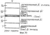
Фиг.30 представляет схематический поперечный разрез альтернативной барьерной структуры, предназначенной для использования во втором типе соответствующего изобретению запоминающего устройства. 30 is a schematic cross-sectional view of an alternative barrier structure for use in a second type of storage device according to the invention.
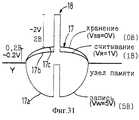
Фиг. 31 представляет диаграмму энергетической зоны проводимости, соответствующей показанной на фиг.30 барьерной структуре. FIG. 31 is a diagram of an energy conduction band corresponding to the barrier structure shown in FIG.
Фиг. 32 представляет схематический поперечный разрез третьего типа соответствующего изобретению запоминающего устройства. FIG. 32 is a schematic cross-sectional view of a third type of storage device according to the invention.
Подробное описание изобретения
В последующем описании соответствующие изобретению варианты осуществления запоминающего устройства можно классифицировать по трем различным типам.DETAILED DESCRIPTION OF THE INVENTION
In the following description, embodiments of the storage device according to the invention can be classified into three different types.
Тип 1
На фиг.1 показана общая конфигурация первого типа соответствующего изобретению запоминающего устройства. Узел памяти 1 и барьерная структура 2 объединены внутри управляющего электрода полевого транзистора, имеющего выводы истока и стока S, Y и вывод управляющего электрода X. Когда информация запоминается, носители заряда туннелируют через барьерную структуру 2 в узел памяти 1, и устройство действует как запоминающий конденсатор, так что заряд удерживается в узле 1. Для считывания информации проводимость канала исток-сток S, Y контролируется и изменяется между относительно высоким и относительно низким состояними проводимости в зависимости от уровня заряда, хранящегося в узле памяти 1.
1 shows a general configuration of a first type of storage device according to the invention. The
На фиг. 2 показана вольт-амперная характеристика барьерной структуры 2, где V - напряжение узла памяти. Поток электронов I через барьерную структуру от вывода Х сильно подавляется в области блокирования VP, которая проходит между верхним и нижним пороговыми напряжениями ±VC. Однако вне этой области запирающего напряжения носители заряда могут туннелировать в узел памяти 1 или из него через барьерную структуру, в зависимости от полярности смещающего напряжения VX, прикладываемого к выводу X. Барьерную структуру можно рассматривать как многотуннельный переход, в котором два или больше туннельных перехода соединены последовательно.In FIG. 2 shows the current-voltage characteristic of the
Показанное на фиг.1 запоминающее устройство можно использовать в качестве ячейки памяти в матрице из таких устройств, расположенных в рядах и столбцах, как показано на фиг.3, со связанными с ними линиями слов X1, Х2 и т. д. и линиями двоичных разрядов S1, Y1, S2, Y2 и т.д. Таким образом, матрица включает в себя ячейки памяти Мmn, где m и n представляют номера рядов и столбцов, соответственно.The storage device shown in FIG. 1 can be used as a memory cell in a matrix of such devices arranged in rows and columns, as shown in FIG. 3, with associated lines of words X1 , X2 , etc., and lines binary digits S1 , Y1 , S2 , Y2 , etc. Thus, the matrix includes memory cells Mmn , where m and n represent the numbers of rows and columns, respectively.
Первый вариант осуществления изобретения
Теперь рассмотрим структуру первого варианта осуществления ячейки памяти Мmn со ссылкой на фиг.4, 5 и 6, где фиг.4 представляет вид сверху матрицы ячеек, а фиг.5 и 6 являются поперечными разрезами, взятыми по линии А-А' и В-В' фиг.4, соответственно, ячейки М11.First Embodiment
Now, consider the structure of the first embodiment of the memory cell Mmn with reference to FIGS. 4, 5 and 6, where FIG. 4 is a plan view of a matrix of cells, and FIGS. 5 and 6 are cross-sectional views taken along line A-A 'and B -B 'figure 4, respectively, of the cell M11 .
Рассмотрим фиг.5, где устройство образовано в подложке 3, которая в данном примере содержит полупроводниковую подложку р-типа, в которой проводящий канал 4 проходит между истоком n+ и областями стока 5, 6. Электроизоляционная область SiO2 7 изолирует ячейку от следующей ячейки в матрице. Подложку закрывает электроизоляционный слой SiO2 8. Узел памяти 1 и закрывающая его конфигурация 2 туннельного перехода образованы в области, окруженной слоем 8. Проводящий управляющий электрод 9 накрывает конфигурацию 2 туннельного перехода. Управляющий электрод 9 образует линию слов Х1, которая проходит по ряду матрицы. Области истока и стока 5, 6 образуют линии двоичных разрядов S1, Y1, которые проходят по столбцу матрицы, показанной на фиг.4. Должно быть понятно, что другие ячейки в матрице имеют соответственные линии слов и двоичных разрядов.Consider figure 5, where the device is formed in a
Узел памяти 1 состоит из точечных элементов или гранул нанометрического масштаба, ограничивающих количество электронов, которые могут запоминаться путем зарядки через барьерную конфигурацию 2 так, чтобы обеспечить однородное поле в боковом направлении по узлу. The
Теперь будет описан процесс избирательных записи и считывания данных для ячейки памяти М11 со ссылкой на фиг.7 и 8. В этом процессе линия слов X1 и линии двоичных разрядов S1, Y1, связанные с ячейкой памяти M11, активируются, а другие линии слов и двоичных разрядов заземляются. Когда информация записывается в М11, к линии слов Х1 подводится импульсная форма волны напряжения с положительным пиковым значением VX (W) и отрицательным значением - VX(W). Когда записывается "0", к линиям двоичных разрядов Y1 и S1 подводится положительный импульс напряжения с высотой VY W. С другой стороны, когда записывается "1", импульс напряжения с пиковым значением -VY (W) прикладывается к линиям двоичных разрядов Y1 и S1. Требование к этим импульсам таковы, что они должны перекрываться в течение времени Т. В этом примере VX (W)=1,2 В, VY (W)=1,8 В, а Т=10 нс.Now will be described the process of selective recording and reading of data for the memory cell M11 with reference to Figs. 7 and 8. In this process, the word line X1 and the bit lines S1 , Y1 associated with the
Рассмотрим фиг.8, где количество электронов, которые могут находиться в узле памяти 1, ограничивается протяженностью области блокирования и напряжения конфигурации туннельного перехода 2. Таким образом, напряжение в узле не может превышать ±VC. На фиг.8(а) бит "1" двоичных данных отображается положительно заряженным состоянием 11 (недостаток электронов) в узле памяти 1, тогда как "0" отображается отрицательно заряженным состоянием 12 (избыток электронов) в узле памяти 1. В этом примере напряжения узла памяти в состояниях "1" и "0" составляет +0,4 В и -0,4 В, соответственно. Теперь будет описан процесс записи "0" в узле 1 со ссылкой на фиг.8(е)-8(d), где VSY=VS= VY, a черные точки отображают окончательное электронное состояние, которое возникает на каждом этапе. Как показано на фиг.8(а), положительное напряжение VY (W) (1,8 В) прикладывается к линиям двоичных разрядов S1 и Y1, два состояния 11 и 12 перемещаются в точку 13 (1,6 В) и точку 14 (0,8 В), соответственно, по линии постоянного количества электронов в узле памяти, то есть
V = (Cg/CΣ)VSY+VO, (1)
где CΣ представляет общую емкость узла памяти, Сg представляет емкость между узлом памяти и клеммам Y1 и S1, а VO - напряжение узла памяти, когда VSY = O(-CΣVO/q представляет количество избыточных электронов в узле памяти, где q - элементарный заряд). В настоящем варианте осуществления CΣ/Cg = 1,5.
Когда отрицательное напряжение - VX (W)(-1,2 В) прикладывается к линии слов Х1, как показано на фиг.12b, область блокирования VB смещается, как показано, состояние 13 переходит в состояние 14, поскольку состояние 13 находится вне области блокирования и не может здесь существовать.Consider Fig. 8, where the number of electrons that can be in the
V = (Cg / CΣ ) VSY + VO , (1)
where CΣ represents the total capacity of the memory node, Cg represents the capacity between the memory node and terminals Y1 and S1 , and VO is the voltage of the memory node when VSY = O (-CΣ VO / q represents the number of excess electrons in memory node, where q is the elementary charge). In the present embodiment, CΣ / Cg = 1.5.
When a negative voltage - VX(W) (-1.2 V) is applied to the word line X1 , as shown in Fig. 12b, the blocking region VB is shifted, as shown,
Когда положительное напряжение VX (W) (1,2 В) прикладывается к линии слов X1, как показано на фиг.12с, это состояние сохраняется. Затем линия слов и линии двоичных разрядов заземляются, как показано на фиг.12d, а состояние 14 переходит в "0" состояние 12 по линии постоянного количества электронов в узле памяти 1.When a positive voltage VX(W) (1.2 V) is applied to the word line X1 , as shown in FIG. 12c, this state is maintained. Then the line of words and lines of binary digits are grounded, as shown in fig.12d, and
Следует отметить, что любое состояние электронов между состояниями "0" и "1" 11, 12 обновляется с помощью процесса для установления состояния "0". Соответственный процесс для записи состояния "1" 11 показан на фиг.8е-8h. В этой последовательности любое состояние между состояниями "0" и "1" изменяется на обновление состояния "1". It should be noted that any state of electrons between the states “0” and “1” 11, 12 is updated by a process for establishing the state “0”. A corresponding process for recording state “1” 11 is shown in FIGS. 8e-8h. In this sequence, any state between states “0” and “1” changes to update state “1”.
Можно заметить, что процесс записи требует одновременной подачи форм сигналов записи на линии двоичных разрядов и линию слов, связанные с конкретной ячейкой памяти. Таким образом, можно индивидуально адресовать ячейки памяти. Во время процесса записи область блокирования смещается последовательно вверх и вниз таким образом, чтобы принудить состояния электронов в узле селективно принимать значение либо "1", либо "0". Однако, если сигнал записи прикладывается к линии слов X1, но не к линиям двоичных разрядов Y1 и S1, или сигналы записи прикладываются к линиям двоичных разрядов, но не к линии слов, запись произведена не будет, и в узле 1 сохранится существующее состояние.You may notice that the recording process requires the simultaneous filing of the waveforms of the recording on the binary line and the word line associated with a particular memory cell. Thus, memory cells can be individually addressed. During the recording process, the blocking region is shifted sequentially up and down so as to force the states of the electrons in the node to selectively take the value either "1" or "0". However, if the write signal is applied to the word line X1 , but not to the binary lines Y1 and S1 , or if the write signals are applied to the binary lines, but not to the word line, the recording will not be performed, and the existing node will be saved in
Для считывания хранящейся информации положительное напряжение затвора VX (r) прикладывается к линии слов Х1 и определяется ток ISY между S1 и Y1. Как показано на фиг.9, пороговое напряжение транзистора задается напряжением VT, когда узел памяти 1 заряжен отрицательно ("0"), и величиной Vt-ΔVT, тогда узел памяти заряжен положительно ("1"). Эти пороговые напряжения VT и VT-ΔVT положительные, так что в невыбранных ячейках памяти электрический ток между S и Y не течет (VX=0). Напряжение затвора VX (r) нa выбранной линии слов выбирается между VT-ΔVT и ΔVT. Таким образом, ISY>0 для "1" и ISY=0 для "0". Таким образом, можно использовать детектор тока (не показанный) для обнаружения тока, текущего между линиями двоичных разрядов Y1 и S1 (и другими соответственными частями линий двоичных разрядов в матрице), когда напряжение затвора VX (r) прикладывается к линии слов Х1. Для того чтобы считывать данные из всей матрицы памяти, процесс последовательно повторяется для других линий слой Х матрицы. В настоящем варианте осуществления изобретения, V(r)X=0,8 В, VT-ΔVT=0,4 В и VT=1,2 В. В соответствии с изобретением, конфигурация туннельного перехода 2 увеличивает время хранения и улучшает характеристику считывания-записи. Время хранения узла 1 определяется способностью конфигурации туннельного перехода 2 подавлять течение электронов в блокированной области VB показанной на фиг.2 вольт-амперной характеристики. Время хранения tS приблизительно задается с помощью выражения
tS=tWexp(-qVC/kT), (2)
где k - постоянная Больцмана, Т - абсолютная температура, q - элементарный заряд, a tW - время записи. Желательно, чтобы обеспечить, например, время хранения tS, равное десяти лет, и tW, равное 10 нс, напряжение VC должно быть больше 1 В для работы при комнатных температурах. Если бы необходимо было использовать эффект от заряда одного электрона, то потребовало бы образования барьерной структуры 2 из металлических частиц размером менее 1 нм, чего нельзя легко добиться с помощью существующих в настоящее время технологий изготовления.To read the stored information, a positive gate voltage VX(r) is applied to the word line X1 and the current ISY between S1 and Y1 is determined. As shown in FIG. 9, the threshold voltage of the transistor is set by a voltage VT when the
tS = tW exp (-qVC / kT), (2)
where k is the Boltzmann constant, T is the absolute temperature, q is the elementary charge, and atW is the recording time. It is desirable to provide, for example, a storage time tS of ten years and tW of 10 ns, the voltage VC must be greater than 1 V for operation at room temperature. If it were necessary to use the effect of the charge of one electron, then it would require the formation of a
В способе, с помощью которого можно достичь повышенного запирающего напряжения VC, используется эффект искривления энергетической зоны для барьерной конфигурации 2 заряда, который описан непосредственно в связи с многотуннельным переходом в работе К. Наказато и Х. Ахмеда, "Журнал прикладной физики", 5 июня 1995 г., том 66, 23, стр.3170-3172. Характеристики, необходимые для туннельного перехода для циклов хранения и записи, можно рассматривать отдельно. Для цикла хранения высоту и ширину туннельного перехода можно обозначить символами фS и dS, соответственно, а для цикла записи фW и dW. Для сохранения запомненной информации в течение более 20 лет высота барьера фS должна быть больше 1,8 эВ для подавления термически активируемого тока эмиссии Пула-Френкеля, а толщина туннельного перехода dS должна быть толще 8 нм•{фS(эВ)}-1/2 для управления туннельным током утечки. Однако для получения небольшого времени записи, примерно 10 нс, ширина dW туннельного перехода должна быть меньше, чем 2 нм • {фW(эВ)}-1/2, где фw является высотой барьера для цикла записи.In the method with which it is possible to achieve an increased blocking voltage VC , the effect of curvature of the energy zone for the barrier configuration of
Барьерная конфигурация 2, которая может удовлетворить этим критериям, показана на фиг. 10 и содержит многотуннельный переход, состоящий из слоев 15, 16 электроизоляционного и неэлектроизоляционного материала, соответственно. В этом примере электроизоляционные слои 15 содержат 1-3 нм толщины Si3N4, а неэлектроизоляционные слои 16 содержат поликристаллический кремний толщиной 3-10 нм.A
Полученная в результате диаграмма энергетической зоны проводимости для показанной на фиг.10 барьерной конфигурации 2 иллюстрируется на фиг.11 и содержит первый относительно широкий барьерный компонент 17, с шириной BW1, соответствующей объединенной ширине всех слоев 15, 16, которые составляют барьерную конфигурацию 2. Кроме того, каждый из электроизоляционных слоев 15 дает повышение сравнительно узкой барьерной компоненты 18а, 18b и т.д., каждый из которых имеет ширину ВW2, разнесенных друг от друга посредством запирающих областей, которые в данном случае образованы из слоев 16 из поликристаллического кремния. Относительно широкий барьерный компонент 17 имеет относительно низкую барьерную высоту Bh1, в то время как барьерные компоненты 18а, 18b и т.д. обеспечивают значительно более высокие барьеры Вh2а, Bh2b.The resulting diagram of the energy conduction band for the
Два компонента 17, 18 барьера выполняют разные роли. Узкие и высокие барьерные компоненты 18 действуют как туннельные переходы, которые сдерживают эффект объединенного туннелирования, а именно, спонтанное туннелирование через два или более туннельных перехода за счет механического эффекта квантования, так что электроны перемещаются только через один барьер 18 одновременно и остаются в течение некоторого периода времени в области между ними. Во время нахождения в этой области электроны неупруго рассеиваются по направлению к локальному состоянию равновесия, регулируемому энергией широкого барьерного компонента 17. Таким образом, на перенос электронов оказывает сильное воздействие широкий барьерный компонент 17. Ширину и высоту высоких, узких барьерных компонентов 18 нельзя изменять с помощью внешних смещений, поскольку они определяются материалами, образующими барьерную конфигурацию 2. Однако компонент широкого, низкого барьера 17 можно модулировать с помощью внешних смещений. The two
На фиг.11а показана диаграмма зоны при отсутствии прикладываемого напряжения VX. Можно заметить, что когда к управляющему электроду 9 не прикладывается напряжение, электрон 20 в узле 1 хранения заряда вынужден туннелировать через всю ширину относительно широкого барьерного компонента 17, если имеется утечка из узла 1, в результате чего утечка заряда сильно подавляется. Однако, когда к электроду 9 прикладывается напряжение, диаграмма энергетической зоны проводимости для барьера 2 изменяется до конфигурации, показанной на фиг.11b, из которой можно заметить, что приложенное напряжение заставляет относительно широкий барьерный компонент 17 образовывать идущий вниз уклон по направлению к узлу 1 хранения заряда, в результате чего электрон 20 вынужден туннелировать только через относительно узкие барьерные компоненты 18 для того, чтобы достичь узла хранения. Таким образом, барьерная конфигурация обеспечивает относительно широкий барьерный компонент 17 для долговременного хранения электронов в узле 1, не требуя приложения крайне высоких напряжений к электроду 9 для того, чтобы заставить электроны туннелировать в узел 1 во время процесса записи.On figa shows a diagram of the zone in the absence of the applied voltage VX. You can see that when no voltage is applied to the
В слоях 16 гранулы поликристаллического кремния имеют диаметр, у которых почти такой же размер, как толщина. Размер гранул в узле памяти 1 может быть больше, чем размер слоев 16, в результате чего электроны могут устойчиво храниться в узле памяти 1 с целью обеспечения надежного функционирования. В устройстве на фиг.10 узел памяти 1 имеет толщину 5-30 нм и образован из поликристаллического кремния. В модификации узел 1 можно легировать для улучшения стабильности состояний электронов в узле. Из вышеизложенного видно, что при запоминании информации слои 17 поликристаллического кремния образуют области перехода и таким образом увеличивают dS, тогда как в процессе записи слои 16 не действуют в качестве барьера, а вместо этого устройство обеспечивает градиент потенциала, который ускоряет электроны от электрода 9 по направлению к узлу 1, что способствует быстрой записи электронов в узел.In layers 16, the polycrystalline silicon granules have a diameter that is almost the same size as the thickness. The size of the granules in the
Теперь будет описан более подробно пример изготовления устройства со ссылкой на фиг.12. Для подложки 3 используется пластинка из кремния р-типа с удельным сопротивлением 10 Ом-см. Сначала образуют электроизоляционный слой 7 из непроводящего SiO2 толщиной 500 нм. После образования электроизоляционного слоя 7, с помощью термического окисления на верхнюю часть кремниевой подложки 3 р-типа наращивают оксидную пленку затвора 21 толщиной 10 нм. Затем наносят слой, который предназначен для образования узла памяти 1. Слой 1 содержит Si n-типа, нанесенный толщиной 10 нм, имеющий поверхность, преобразованную в нитрид кремния в атмосфере NH3 при температуре 900oС. Толщина получающегося в результате нитрида кремния самоограничивается 2 нм. Это соответствует показанному на фиг.10 слою нитрида 15а. После этого наносят слой нелегированного кремния толщиной 5 нм так, чтобы образовать покрывающий слой 16а (фиг. 10), который затем подвергают азотированию для образования следующего слоя 15b нитрида кремния 2 нм толщины. Для построения барьерной структуры 2 процесс повторяют несколько раз.Now will be described in more detail an example of the manufacture of the device with reference to Fig. For the
Затем на слой барьерной структуры 2 наносят пленку 22 легированного кремния n-типа толщиной 20 нм. На пленку 22 наносят пленку 23 из SiQ2 толщиной 20 нм методом химического осаждения в паровой фазе (ХОПФ).Then, a film of doped silicon n-
Различные слои кремниевой пленки наносят в аморфном состоянии, но они преобразуются в поликристаллический кремний во время азотирования и процесса загустения при ХОПФ осаждаемого слоя 23 SiO2, затем верхнюю часть пленки 23 SiO2 структурируют с помощью обычных методов литографии и реактивного ионного травления в атмосфере CHF3 и газообразного аргона.The various layers of the silicon film are deposited in an amorphous state, but they are converted to polycrystalline silicon during nitriding and the thickening process during CVD of the deposited 23 SiO2 layer, then the upper part of the 23 SiO2 film is structured using conventional lithography and reactive ion etching in an atmosphere of CHF3 and gaseous argon.
Затем, используя структурированный слой 23 SiO2 в качестве маски, слои 22, 2 и 1 поликристаллического кремния и нитрида кремния протравливают с помощью реактивного ионного травления, используя CF4 для образования конфигурации затвора 24, как показано на фиг.12b. Конфигурация затвора 24 обычно имеет длину 1, равную 0,15 мкм.Then, using the structured SiO2 layer 23 as a mask, the polycrystalline silicon and silicon nitride layers 22, 2, and 1 are etched using reactive ion etching using CF4 to form the configuration of the
После этого пластинку оксидируют для образования наружного слоя 25 толщиной 30 нм термического SiO2, как показано на фиг.12с. Затем с помощью ионной имплантации ионами мышьяка формируются области истока и стока 5, 6.After that, the plate is oxidized to form an
Затем, как показано на фиг.12d, наносят 100 нм на пленку 26 SiO2, которую закрывают слоем оптического фоторезиста 27, наносимого достаточной толщиной для получения плоской верхней поверхности, в данном примере толщиной 1500 нм. Затем фоторезист 27 опять вытравливают до тех пор, пока верхняя часть слоя 26 SiO2 не выступит сквозь поверхность. Травление выполняют методом распыления в атмосфере O2. Полученная в результате конфигурация показана на фиг.12е.Then, as shown in FIG. 12d, 100 nm is applied to a SiO2 film 26, which is covered with a layer of
Верхнюю часть 26а пленки 26 SiO2 удаляют с помощью реактивного ионного травления в атмосфере газа WF6 до тех пор, пока не покажется верхняя часть пленки 22 поликристаллического кремния, как показано на фиг.12f.The
После удаления оптического фоторезиста 27 на полученную в результате поверхность наносят металл и структурируют с помощью обычных литографических приемов для обеспечения управляющего электрода 9, который образует описанные выше линии слов X1.After removing the
Должно быть ясно, что запоминающее устройство можно модифицировать различными способами. Например, толщина электропроводных слоев 15 может отличаться от описанного значения 5 нм и, в общем, может быть удовлетворительной толщина в 10 нм или меньше. Толщину электроизоляционных слоев 16 можно изменять от описанного выше значения в 2 нм так, чтобы находиться в диапазоне 3 нм или меньше, чтобы образовывать удовлетворительные узкие высокие барьерные компоненты 18, хотя описанный процесс изготовления дает в результате правильное управление толщиной каждого слоя 16 так, что она становится порядка 2 нм. Кроме того, количество наборов слоев 15, 16 может отличаться от описанного в примере семь до достаточных количеств для образования удовлетворительно широкого, узкого барьерного компонента 17 поперек барьерной конфигурации 2. It should be clear that the storage device can be modified in various ways. For example, the thickness of the electrically
Второй вариант осуществления изобретения
В модификации, показанной на фиг.10, барьерную конфигурацию 2 можно заменить конфигурацией барьера Шотки, как показано на фиг.13. В этом случае вместо использования электроизоляционных слоев 15 нитрида кремния используют металлические слои 28 таким образом, чтобы обеспечить множественную конфигурацию диодов Шотки, перекрывающих друг друга. Металлические слои 28 можно делать из W, или они могут содержать пленки из силицида, типа CoSi2, образованные между пленками 16 из нелегированного поликристаллического кремния.Second Embodiment
In the modification shown in FIG. 10, the
Теперь будут описаны следующие соответствующие изобретению варианты осуществления запоминающего устройства, в котором конфигурация 2 туннельного перехода состоит из островков нанометрического масштаба, распределенных в кристаллической решетке из электроизоляционного материала. В последующих примерах островки нано-масштаба имеют диаметр 5 нм или меньше и разделены электроизоляционным материалом с толщиной нанометрического масштаба в кристаллической решетке, например, размером 3 нм или меньше, что дает повышение узким, высоким барьерным компонентам конфигурации туннельного перехода. Узел хранения заряда можно образовывать с помощью проводящих островков так, чтобы они были распределены по барьерной конфигурации, а не образовали отдельный слой 1, как описывалось прежде. Для обеспечения получающейся в результате конфигурации многотуннельного перехода можно использовать несколько различных процессов изготовления, как теперь будет описано. The following embodiments of a storage device in which the
Третий вариант осуществления изобретения
Фиг. 14 иллюстрирует схематическое поперечное сечение другого соответствующего изобретению варианта осуществления запоминающего устройства. В этом варианте осуществления узел памяти 1 и барьерная структура 2 реализованы путем объединения кристаллов нанометрического масштаба, которые распределены в окружающей их кристаллической решетке SiO2. Рассмотрим фиг.14, на которой подложка 3 обеспечена областями истока и стока 5, 6 с каналом 4 между ними. Оксидный слой затвора 29 покрывает канал 4 и имеет толщину 5 нм, образован с помощью процесса термического оксидирования на подложке. После этого наносят слой кремния толщиной 6 нм с помощью электронно-лучевого парообразования или ХОПФ, который затем подвергают быстрому термическому оксидированию и кристаллизации. Этот процесс описан в работе Е.Х. Николиана и Р. Цу, "Журнал прикладной физики", том 74, 1993 г., стр. 4020-4025, и М. Фукуда, К. Накагава, С. Миязаки и М. Хироуза, "Обширные рефераты" (Extended abstrakts) Международной конференции по твердотельным устройствам и материалам, 1996 г., Иокогама, 1996 г. , стр. 175-178. Это образует островки в форме нанокристаллов Si со средним диаметром 3 нм, расположенные в слое 30 с оксидным слоем туннелирования 31 толщиной 2 нм, покрывающим слой 30. Собственная емкость 3 нм кристаллов Si дает энергию зарядки порядка 100 мэВ, которая достаточна для ограничения с помощью блокады Кулона количества электронов внутри каждого нанокристалла, при комнатной температуре. Нанесение слоя 29 с последующим быстрым термическим оксидированием и процессом кристаллизации повторяют несколько раз для построения составного слоя достаточной толщины. В данном варианте осуществления процесс повторялся пять раз для обеспечения толщины объединенного слоя 20 нм, содержащего пять слоев нанокристалла 30 внутри этой толщины. После этого на верхней поверхности образуется контактный слой кремния n-типа 32. Должно быть ясно, что полученную в результате структуру затвора можно включать в описанный выше процесс изготовления запоминающего устройства со ссылкой на фиг.12. Однако должно быть понятно, что узел памяти 1 больше не обеспечивается в качестве отдельного слоя, а вместо этого образуемые в каждом слое 30 нанокристаллы обеспечивают местоположения для хранения электронов, распределенные в электроизоляционных оксидных слоях 29, 31.Third Embodiment
FIG. 14 illustrates a schematic cross-section of another embodiment of a storage device in accordance with the invention. In this embodiment, the
Четвертый вариант осуществления изобретения
Фиг. 15 иллюстрирует этапы процесса для образования другого варианта осуществления запоминающего устройства. В этом варианте осуществления объединение кремниевых нанокристаллов и окружающих слоев SiO2 образовано посредством использования пористых пленок Si. Рассмотрим фиг.15а, где пористая пленка Si 33 толщиной 20 нм образована с помощью анодирования Si р-типа. Анодирование выполняется в 25% водном растворе фтористоводородной кислоты, разведенной этанолом с постоянным анодным током 10 мА/см2 в течение 5 с. В результате образуется составная пленка, содержащая 4~5 нм нанокристаллического Si, внедренного в кристаллическую решетку SiO2. Этот способ известен сам по себе и описывается более подробно в работе Я. Канемицу и др. "Физический обзор" (Phys. Rev.), том В48, 1993 г., стр.2827.Fourth Embodiment
FIG. 15 illustrates process steps for forming another embodiment of a storage device. In this embodiment, a combination of silicon nanocrystals and surrounding SiO2 layers is formed by using porous Si films. 15a, where a
Затем пористая кремниевая пленка 33 термически оксидируется для образования оксидной пленки затвора 34 толщиной 5 нм вместе с верхним оксидным слоем 35 толщиной порядка 7 нм, как показано на фиг.15b. Этот процесс, кроме того, приводит к отжигу, который сокращает диаметр каждого
нанокристалла в пористой Si пленке, а также толщину самого пористого слоя 33. После процесса отжига пористый слой Si 33 имеет толщину 14~16 нм, а средний диаметр частиц уменьшается примерно до 3 нм. Соответствующая энергия заряда для частиц нанокристаллического кремния равна порядка 100 мэВ, которая, как объяснялось выше, приводит к ограничению количества электронов, которые могут проникнуть в узел, из-за блокады Кулона. Полученная в результате пленка обозначена позицией 36 на фиг.15b и содержит приблизительно 3-4 нанокристаллические частицы по своей толщине, благодаря чему обеспечивает многотуннельный переход (МТП) при рассмотрении перемещения электронов вертикально через слой.Then, the
nanocrystal in a porous Si film, as well as the thickness of the
После этого верхний оксидный слой 35 удаляют и наносят затвор 32 из материала поликристаллического кремния, как описывалось выше. Используя затвор 32 из поликристаллического кремния в качестве маски, составную пленку 36 и лежащий под ней оксид затвора 34 удаляют с помощью обычных технических приемов травления и затем имплантируют области истока и стока 5, 6 описанным выше со ссылкой на фиг.12 способом. Этот способ изготовления имеет преимущество по сравнению с описанным со ссылкой на фиг.14 способом, заключающееся в том, что многотуннельный переход образуют с помощью одного процесса анодирования, снижая количество нанесения Si и необходимые этапы оксидирования. After that, the
Пятый вариант осуществления изобретения
Составные материалы нанокристаллов и окружающей кристаллической решетки можно делать другими способами, используя различные материалы. Один пример описан в работе Е. Бар-Садехом и др. "Физический обзор", том В50, 12, 1994 г. , стр.8961-8964. В этом способе слой частиц Аu в кристаллической решетке Аl2О3 можно использовать для замены показанного на фиг.15 пористого кремниевого слоя. Составную пленку 30 нм толщины из Аu и Al2O3 можно делать с помощью совместного напыления золота и алюминия на слой окиси кремния толщиной 5 нм, который образован с помощью термического оксидирования подложки 3. Последующее изготовление устройства такое же, как в четвертом варианте осуществления изобретения. Условия напыления для изготовления составной пленки выбирают так, чтобы реализовать объемное содержание золота, равное 0,4. В этих условиях образуются изолированные частицы Аu в составной пленке, имеющие диаметр порядка 3~5 нм. Следовательно, 30 нм пленка содержит 5~10 частиц Аu по ее толщине, образующих вертикальный МТП. Должно быть ясно, что это можно использовать в качестве подложки для пористого кремниевого слоя, описанного со ссылкой на фиг.15.Fifth Embodiment
Composite materials of nanocrystals and the surrounding crystal lattice can be made by other methods using various materials. One example is described in the work of E. Bar-Sadeh et al. "Physical Review", Volume B50, 12, 1994, pp. 8961-8964. In this method, a layer of Au particles in the Al2 O3 crystal lattice can be used to replace the porous silicon layer shown in FIG. A 30 nm thick composite film of Au and Al2 O3 can be made by co-spraying gold and aluminum onto a 5 nm thick silicon oxide layer that is formed by thermal oxidation of the
С помощью этого способа совместного напыления можно образовывать составные пленки из других благородных металлов, типа Ag, Pt, с какой-нибудь другой кристаллической решеткой из окиси металла, типа SiO2 или Сr2О3.Using this co-deposition method, it is possible to form composite films of other noble metals, such as Ag, Pt, with some other metal oxide crystal lattice, such as SiO2 or Cr2 O3 .
Составную пленку оксидной кристаллической решетки с металлическими островками также можно образовывать путем термического разложения исходных металлических окислов. Например, окись золота, являющаяся исходным металлическим окислом, может быть образована с помощью реактивного распыления мишени из сплава Au - Si в кислородной плазме, как описано в работе Л. Майя и др. в "J. Vac. Sci. Tectnol." (Журнал вакуумной научной технологии), том В14, 1996 г., стр.15-21. A composite oxide crystal lattice film with metal islands can also be formed by thermal decomposition of the starting metal oxides. For example, gold oxide, which is the starting metal oxide, can be formed by reactive sputtering of a target from an Au - Si alloy in oxygen plasma, as described by L. Maya et al. In J. Vac. Sci. Tectnol. (Journal of Vacuum Science Technology), Volume B14, 1996, pp. 15-21.
Шестой вариант осуществления изобретения
На фиг.16 показан способ образования составных нанокристаллов и изоляционных туннельных переходов с помощью способа химического осаждения из коллоидного раствора. Рассмотрим фиг.16а, где оксидный слой 21 толщиной 5 нм образован с помощью процесса термического оксидирования на подложке 3 из Si р-типа. Затем на поверхности слоя 21 из SiO2 производится мономолекулярный слой 37 из октадецил-трихлоросилана (ОТС). Как описывается более подробно в работе М.Дж. Лерсела и др., "J. Vac. Sci. Technol." (Журнал вакуумной научной технологии), том В11, 1993 г., стр.2823-2828. Более подробно, подложку 3 со слоем 21 из SiО2 погружали в раствор 1 миллиграмм-молекулы гексадекана ОТС более чем на 12 часов. В результате получили спонтанное образование мономолекулярного слоя ОТС 37. Молекулы ОТС можно удалить с поверхности SiO2 21 с помощью облучения электронным лучом мощностью 60 кВ. Таким образом, изображения окон в ОТС образуются на мономолекулярном слое 37 с помощью обычной электронно-лучевой литографии. После образования окна в ОТС, подложку погружали в 1% водный раствор фтористоводородной кислоты на 30 с, вымывая остатки облученного электронным лучом ОТС, оставляя окно 38. Краевая область окна показана в увеличенном виде внутри пунктирного контура 39. Показан пример молекулы ОТС 40. Она состоит из цепи алканов, имеющей силоксанную связь на одном конце и метиловую группу на другом. Как показано на увеличенной площадке 39, молекулы 40 образуют силоксановую связь со слоем SiO2 21 и образуют плотно упакованную ковалентно связанную сетку. Метиловая группа на верхнем конце является по существу инертной и, следовательно, очень устойчивой к химическому агрессивному воздействию во время обработки подложки.Sixth Embodiment
On Fig shows a method of forming composite nanocrystals and insulating tunnel junctions using the method of chemical deposition from a colloidal solution. 16a, where an
Затем подложку со структурированным мономолекулярным слоем ОТС 37 поместили в разбавленный (0,05%) безводный раствор толуола (3-Меркаптопропил) триметоксисилана в условиях фракционирования с дефлегмацией (то есть нагревания приблизительно до 100oС) в течение десяти минут. Потом подложку поместили в печь при температуре 105oС на 30 минут для отверждения силоксанных связей. Результат показан на фиг.16b. Эта процедура создает мономолекулярный слой тиола алканов 41 на слое SiO2 21 в области окна 38. Структура отдельных молекул 42, которые образуют мономолекулярный слой тиола алканов, состоит из силоксанной связи на одном конце алкановой цепи с меркаптанной группой на другом. Этот процесс описан более подробно в работе А. Дорона и др., "Langmuir", том 11, 1995 г., стр.1313-1317. Молекулы ОТС вне области окна 38 остаются не затронутыми. Расположение на одной прямой молекул 37, 42 можно видеть более ясно на увеличенном виде края окна, изображенного внутри пунктирной линии 43. В принципе, эту модификацию поверхности можно выполнить с другими алкановыми тиолами, оканчивающимися на одном конце алкоксисиланом ((СН3О)3Si- или (С2H5О)3-Si-).Then, a substrate with a structured monomolecular layer of
Затем подложку погружают в коллоидный раствор золота по меньшей мере на пять часов при комнатной температуре, в результате чего в области окна 38 оказывается прикрепленным мономолекулярный слой коллоидальных золотых частиц 44. Это происходит только в области окна, где поверхность оканчивается меркаптанными группами (-SH), из-за сильного сродства серы с золотом. Средний размер золотых коллоидных частиц составляет 2 нм. Then, the substrate is immersed in a gold colloidal solution for at least five hours at room temperature, as a result of which a monomolecular layer of colloidal gold particles 44 is attached to the
Известно, что коллоидальные частицы золота могут быть приготовлены химическим путем и иметь средние диаметры в диапазоне 2~5 нм с хорошо определенным распределением по размеру, обычно со стандартным отклонением 10%. Такие наночастицы оседают на поверхности, оканчиваемой меркаптанными группами, образуя ковалентные связи между атомом серы в подложке и атомом золота в поверхности золотых коллоидных частиц. Осаждение частиц автоматически прекращается, когда слой приближается к мономолекулярному слою, поскольку электростатические силы, обусловленные поверхностным зарядом золотых частиц, которые обеспечены ионизацией адсорбируемых веществ на золотых коллоидных частицах, предотвращают осаждение других коллоидных частиц на верхней части поверхности подложки или очень близко к уже осажденным там частицам. В отношении более подробного описания мы ссылаемся на наш патент ЕР 96300779.4, зарегистрированный 6 февраля 1996 г. Коллоидальные суспензии таких частиц с заранее определенными средними размерами частиц и распределениями диапазонов диаметров можно приобрести на рынке, у фирмы Нанопробс Инк. (Nanoprobes Inc. ), 25E Луп Роад Сти 124, Стоуни Брук (Stony Brook), Нью-Йорк 11790-3350, США. Частицы подаются в водной суспензии. Адсорбированные ионы цитрата сообщают отрицательный заряд частицам Аu. It is known that colloidal gold particles can be chemically prepared and have average diameters in the range of 2 ~ 5 nm with a well-defined size distribution, usually with a standard deviation of 10%. Such nanoparticles settle on a surface terminated by mercaptan groups, forming covalent bonds between the sulfur atom in the substrate and the gold atom in the surface of the gold colloidal particles. Particle deposition automatically stops when the layer approaches the monomolecular layer, since the electrostatic forces due to the surface charge of the gold particles, which are ensured by ionization of the adsorbed substances on the gold colloidal particles, prevent the deposition of other colloidal particles on the upper surface of the substrate or very close to the particles already deposited there . For a more detailed description, we refer to our patent EP 96300779.4, registered on February 6, 1996. Colloidal suspensions of such particles with predetermined average particle sizes and diameter range distributions can be obtained on the market from Nanoprobes Inc. (Nanoprobes Inc.), 25E Loop Road Sti 124, Stony Brook, New York 11790-3350, USA. The particles are fed in an aqueous suspension. Adsorbed citrate ions impart a negative charge to Au particles.
Затем подложку погружают в 5 миллиграмм-молекулярный этаноловый раствор дитиола (а именно, 1,6-гександитиол) после описанного выше осаждения золотых частиц из коллоидного раствора. Один из двух атомов серы в дитиоле образует связи Au- S с золотой коллоидной поверхностью, замещая поверхностные адсорбируемые вещества золотых частиц дитиолами, тогда как другой конец атома серы в дитиоле ориентирован от золотой поверхности в форме свободной меркаптанной группы. Это расположение показано на фиг.16d с молекулами дитиола, обозначенными ссылочной позицией 45. Следовательно, поверхность золотых частиц преобразовывается в поверхность, покрытую меркаптанной группой, которая может принимать дополнительный слой золотых частиц. The substrate is then immersed in a 5 milligram molecular ethanol dithiol solution (namely, 1,6-hexanedithiol) after the above-described deposition of gold particles from a colloidal solution. One of the two sulfur atoms in dithiol forms Au – S bonds with the gold colloidal surface, replacing the surface adsorbed substances of gold particles with dithiols, while the other end of the sulfur atom in dithiol is oriented from the gold surface in the form of a free mercaptan group. This arrangement is shown in FIG. 16d with dithiol molecules indicated at 45. Consequently, the surface of the gold particles is transformed into a surface coated with a mercaptan group that can receive an additional layer of gold particles.
Далее, обработанную дитиолом поверхность снова погружают в золотой коллоидный раствор для осаждения дополнительного слоя. Этот процесс повторяют пять раз для образования пяти слоев 2 нм золотых частиц, которые соединяются с помощью алкановых цепей дитиола. Два из золотых уровней 46, 47 показаны на увеличенном разрезе 48 на фиг.16b. Полученная в результате структура из пяти слоев золота, имеющая толщину порядка 10 нм, обозначена на фиг. 16d ссылочной позицией 49. Further, the surface treated with dithiol is again immersed in a gold colloidal solution to deposit an additional layer. This process is repeated five times to form five layers of 2 nm gold particles, which are connected using dithiol alkane chains. Two of the
После этого, как показано на фиг.16е, процесс осаждения золота повторяется еще пять раз с золотым коллоидным раствором, который содержит золотые частицы большего размера, например, 40 нм. С помощью этого процесса образуется составной слой 50 из 40 нм золотых частиц толщиной 150 нм на верхней части слоя 49. Поскольку частицы, которые образуют слой 50, имеют значительно больший диаметр, они проявляют пренебрежимо маленькую энергию заряда порядка 1 мэВ и, следовательно, электронная электропроводность через составной слой 50 проявляет омический характер, в отличие от меньших частиц, которые образуют слой 49, демонстрирующих характеристики проводимости, над которыми доминирует эффект блокады Кулона. Поэтому структура 50 из больших золотых частиц функционирует как обычный металлический слой и, следовательно, выполняет функцию затвора таким же образом, как, например, затвор 22 из поликристаллического кремния, описанный в предыдущих вариантах осуществления изобретения. After that, as shown in FIG. 16e, the gold deposition process is repeated five more times with a gold colloidal solution that contains larger gold particles, for example, 40 nm. Using this process, a
После этого золотой составной слой 50 используют как массу для сухого травления слоя ОТС 37 и оксидного слоя затвора 21 так, чтобы обеспечить возможность имплантировать области истока и стока 5, 6 в поверхность 3 с помощью обычных ионно-лучевых технических приемов. After that, the
Тип 2
На фиг.17 показана общая конфигурация другого типа соответствующего изобретению запоминающего устройства. Устройство аналогично показанному на фиг. 1 и подобные части обозначены теми же самыми ссылочными позициями. Устройство фиг. 17 дополнительно включает управляющий затвор 51, который позволяет селективно прикладывать поле к барьерной конфигурации 2 таким образом, чтобы изменять ее характеристики туннельного перехода. Таким образом, когда к выводу Y прикладывается напряжение, то благодаря изменению напряжения на выводе Х поле на затворе 51 может изменяться, и, в результате этого, поле изменяет характеристики туннельного перехода в переходе 2. Влияние поля, прикладываемого с помощью затвора 51, можно видеть на графиках фиг.18. Напряжение на затворе 51 можно использовать для переключения устройства между состояниями "включено" и "выключено", иллюстрируемыми на фиг.18а и 18b соответственно. Прикладываемое к затвору 51 напряжение меняет ширину запирающего напряжения VB. Как показано на фиг.18а, когда напряжение VX "включено" прикладывают к затвору 51, запирающее напряжение является относительно небольшим и в некоторых условиях отсутствует. На фиг.18а запирающее напряжение VB простирается от - VCL до + VCL, тогда как в случае другого напряжения "выключено" на затворе 51 блокирующая область приобретает более широкий диапазон, простирающийся от - VCH до +VCH. Таким образом, когда устройство переключается на состояние "включено", заряд может туннелировать в узел памяти 1 и храниться в течение состояния "выключено". Во время состояния "выключено" смещающее напряжение можно прикладывать к затвору 51 по существу для усиления VCH, как описано в работе К. Наказато и Х. Ахмеда. "Журнал прикладной физики", 5 июня 1995 г., том 66, 23, стр.3170-3172. Создаваемое напряжением VX поле, подаваемое на линию слов 51, прикладывают к конфигурации барьерного перехода 3 таким образом, чтобы сжать непроводящую область, как можно заметить при сравнении фиг.18а с 18b.
17 shows a general configuration of another type of storage device according to the invention. The device is similar to that shown in FIG. 1 and similar parts are denoted by the same reference numerals. The device of FIG. 17 further includes a
Теперь будет представлено более подробное описание со ссылкой на фиг.19 и 20 модуляции области запирающего напряжения для туннельного перехода 2 с помощью затвора 51. Фиг.19 иллюстрирует разрез узла памяти 1, конфигурации барьерного перехода 2 и вывода Y. Затвор 51 опущен на фиг.19, но будет описан ниже. Конфигурация туннельного перехода 2 состоит из чередующихся слоев 15, 16 нелегированного поликристаллического кремния толщиной 3-10 нм и нитрида кремния толщиной 1-3 нм, образованных описанным выше со ссылкой на фиг. 10 образом. Узел памяти 1 состоит из слоя легированного поликристаллического кремния n-типа толщиной 5-30 нм и закрывается слоем 52 нелегированного поликристаллического кремния толщиной 30 нм. Соответствующий нелегированный слой 53 расположен на другой стороне конфигурации перехода, под слоем 54 легированного поликристаллического кремния n-типа толщиной 30 нм. A more detailed description will now be provided with reference to FIGS. 19 and 20 of the modulation of the blocking voltage region for the
Как можно видеть из диаграммы энергетической зоны на фиг.20, семь электроизоляционных слоев 15 нитрида кремния дают повышение соответственным относительно узким и относительно высоким барьерным компонентам 18 аналогичным описанному со ссылкой на фиг.11 образом, вместе с относительно широким, но низким барьерным компонентом 17. Эффект от прикладывания напряжения к затвору 51 заключается в повышении и понижении барьерного компонента 17 по выбору, вместе с барьерными компонентами 18, которые, соответственно, увлекаются вверх и вниз. As can be seen from the energy zone diagram of FIG. 20, seven silicon
В процессе записи напряжение VX, прикладываемое к выводу Х (фиг.17), устанавливают на напряжение записи VW (OV) и в результате высота широкого барьерного компонента 17, которая фактически является внутренним электростатическим потенциалом в конфигурации перехода, в данном примере является относительно низкой величиной порядка 0,2 В. Таким образом, электроны могут туннелировать через узкие барьерные компоненты 18 и не задерживаются низким широким барьерным компонентом 17а, так что электроны туннелируют из вывода Y в узел памяти 1.During the recording process, the voltage VX applied to terminal X (FIG. 17) is set to the recording voltage VW (OV) and, as a result, the height of the
Хранящийся заряд в узле 1 может удерживаться, благодаря повышению VX до вспомогательного напряжения VSB, в данном примере равно -5 В. Это увеличивает общую высоту относительно широкого барьерного компонента 17 до уровня 17 b, который в данном примере составляет порядка 3 В. Полученное в результате увеличение высоты барьерного компонента 17 сдерживает туннелирование носителей заряда из узла памяти 1 так, что информация может сохраняться в узле длительные периоды времени ~10 лет.The stored charge in
Для считывания информации VX устанавливают на напряжение считывания VR, которое в данном примере составляет порядка -4 В. Как будет описано ниже, это удерживает заряд, хранящийся в узле памяти 1, но позволяет считывать информацию из канала исток-сток устройства в течение относительно короткого цикла считывания, равно ~100 нс. Барьерный компонент 17 принимает форму 17с, показанную на фиг.20.To read information, VX is set to a read voltage VR , which in this example is of the order of -4 V. As will be described below, this retains the charge stored in the
Седьмой вариант осуществления изобретения
Теперь будет описана более подробно структура матрицы таких устройств со ссылкой на фиг.21, которая изображает прямоугольную матрицу из четырех ячеек на горизонтальной проекции, совместно с фиг.22 и 23, которые иллюстрируют разрезы по одной из ячеек, вдоль линий А-А' и В-В' фиг.21, соответственно. Рассмотрим фиг.22, где общая структура каждой ячейки памяти аналогична структуре первого типа, как показано на фиг.5, но с дополнением затвора 51, а те же самые каналы обозначены такими же ссылочными позициями. Рассмотрим фиг. 22, где подложка 3 р-типа включает в себя проводящий канал 4 между областями истока и стока 5, 6 вместе с электроизоляционной областью 7 для изоляции одной ячейки от другой. Устройство включает узел памяти 1 и лежащую поверх барьерную структуру 2, образованную, как показано на фиг.19, с покрывающим их слоем 53 нелегированного поликристаллического кремния и линией двоичных разрядов, образованной слоем 54 легированного поликристаллического кремния n-типа. Линия двоичных разрядов 54 закрывается электроизоляционными ХОПФ SiO2 55 и стенками SiO2 56, как будет описано более подробно ниже. Боковой затвор 51 для ячейки состоит из слоя поликристаллического кремния n-типа толщиной 100 нм, который проходит поперек линии двоичных разрядов и накрывает боковые кромки 57 барьерной структуры 2.Seventh Embodiment
Now will be described in more detail the structure of the matrix of such devices with reference to Fig, which depicts a rectangular matrix of four cells on a horizontal projection, together with Fig and 23, which illustrate cuts along one of the cells, along lines aa 'and B-B 'of Fig. 21, respectively. Consider FIG. 22, where the overall structure of each memory cell is similar to the structure of the first type, as shown in FIG. 5, but with the addition of
Рассмотрим вновь фиг.21, на которой видно, что стоки 6 для соседних ячеек памяти в конкретном ряду делают с использованием общей области стока 6, что снижает размер ячейки памяти. Let us consider again FIG. 21, which shows that the
Информацию можно записывать в конкретную ячейку, например, ячейку памяти М11, показанную на фиг.21, прикладывая напряжение записи VW к линии слов X1 (51) и подходящее напряжение к линии двоичных разрядов Y1 (54) в зависимости от двоичного кода "0" или "1". Это вызывает запись заряда в узле памяти 1 ячейки памяти М11, соответствующей двоичному "0" или "1", в зависимости от напряжения линии двоичных разрядов Y1. Данные не записываются в другие ячейки памяти в столбце, поскольку на линии слов Х2 и т.д. других ячеек поступает вспомогательное напряжение VSB. После этого к линии слов Х1 прикладывают вспомогательное напряжение VSB для сохранения данные в узле 1 ячейки М11. На линии двоичных разрядов не следует подавать напряжение. Когда требуется считывать хранящиеся данные из ячейки М11, напряжение считывания VR на линии слов X1 подается более низкое, чем вспомогательное напряжение VSB. Периферийные схемы (не показанные) воспринимают проводимость истока-стока ячейки M11, считывая ток, протекающий между линиями S1 и G (линии 5, 6). Другие ячейки памяти в столбце смещаются с помощью вспомогательного напряжения VSB, прикладываемого к их линиям слов Х2, и т.д., и таким образом эти ячейки не адресуются при считывании М11.Information can be recorded in a specific cell, for example, memory cell M11 shown in FIG. 21, by applying a write voltage VW to the word line X1 (51) and a suitable voltage to the binary line Y1 (54) depending on the binary code "0" or "1". This causes a charge to be recorded in the
Кроме того, можно использовать другой способ работы схемы, аналогичный обычному способу, применяемому при обычных ДЗУПВ, в котором хранящаяся информация передается в периферийные схемы и затем заменяется на новую информацию, которая записывается в каждом узле памяти. Этот способ имеет преимущество, разрешая широкие допустимые отклонения в расчетной величине диапазона запирающего напряжения VB, посредством чего допуская появление существенных изменений значений VCL и VCH в различных ячейках. Двоичная "1" представляется напряжением узла памяти VH, а двоичный "0" представляется напряжением узла памяти VL. В отношении схемы существует только требование, чтобы VCH было больше, чем VH, и чтобы VСL было меньше, чем VL, то есть VCH>VH>VL>VCL, и фактически нет необходимости определять их величины. Этот широкий расчетный допуск делает возможным объединение большого количества ячеек памяти в микросхеме.In addition, you can use a different method of operation of the circuit, similar to the conventional method used with conventional DRAM, in which the stored information is transmitted to peripheral circuits and then replaced with new information that is recorded in each memory node. This method has the advantage of allowing wide tolerances in the calculated value of the blocking voltage range VB , whereby allowing the occurrence of significant changes in the values of VCL and VCH in different cells. Binary "1" is represented by the voltage of the memory node VH , and binary "0" is represented by the voltage of the memory node VL. Regarding the scheme, there is only a requirement that VCH be greater than VH , and that VCL be less than VL , that is, VCH > VH > VL > VCL , and in fact there is no need to determine their values. This wide design tolerance makes it possible to combine a large number of memory cells in the chip.
Теперь будет приведено подробное описание этого способа работы со ссылкой на фиг.24-26. Фиг.24 схематически иллюстрирует электрическую схему матрицы ячеек памяти, соответствующую фиг.21, и дополнительно показывает периферийные схемы, которые объединены на той же полупроводниковой подложке 3, что и матрица ячеек памяти. Каждая ячейка памяти М11-Мmn соответствует запоминающему устройству второго типа, как описывалось выше, хотя схема представлена эквивалентной схемой, состоящей из двух транзисторов QR и QR. Узел памяти 1 представлен индексом N. На фиг.24 показана конфигурация для ячейки памяти М11. Интегральная схема включает декодер и драйвер столбца 58, декодер и драйвер ряда 59, находящийся в микросхеме преобразователь напряжения VC, который создает ряд управляющих напряжений, описываемых более подробно ниже, от внешнего источника напряжения VСС, который в данном примере является источником напряжения 5 В. Каждый столбец матриц ячеек памяти имеет связанную с ним схему предварительной зарядки 60 (PC) и схему считывания-перезаписи 61 (RWC), PC 60 и RWC 61 подробно показаны для столбца n=1 матрицы ячеек памяти, а соответствующие схемы для столбца n показаны в пунктирном контуре.A detailed description will now be given of this method of operation with reference to FIGS. 24-26. 24 schematically illustrates an electrical circuit of a matrix of memory cells corresponding to FIG. 21, and further shows peripheral circuits that are combined on the
Схема ввода-вывода данных 62 принимает данные из внешнего источника и передает данные из матрицы памяти способом, описанным более подробно ниже. A data input /
Система условных обозначений различных сигналов, линий и компонентов, используемых на фиг.24, 25 и 26, суммирована в таблице. The system of symbols for various signals, lines and components used in Figs. 24, 25 and 26 is summarized in the table.
Теперь будет подробно описан процесс считывания данных со ссылкой на фиг. 25. Когда сигнал разблокирования микросхемы СЕ имеет уровень напряжения VCC, далее обозначаемый как "высокий", микросхема неактивна. В этих условиях сигнал предварительной зарядки фр является "высоким", a S1... Sn, Y1...Yn и I/O предварительно заряжаются до напряжения VP, потому что транзисторы в PC 60 находятся в "открытом" состоянии. Когда СЕ заряжается от "высокого" до нулевого напряжения (далее обозначаемого как "низкое"), микросхемы становятся активными. Затем фр становится "низким" для переключения транзисторов PC 60 в "запертое" состояние. После этого напряжения линий S1... Sn, Y1...Yn плавают, сохраняя величину напряжения VP. Линия слов выбирается с помощью подачи сигналов адреса ряда (аxi) на драйвер ряда 59. Когда напряжение считывания VR прикладывается к Х1, из первого ряда ячеек памяти М11...М1n считывается информация, а выходные сигналы появляются на соответствующих линиях считывания, S1. .. Sn. Рассматривая, в качестве примера, ячейку памяти М11, когда напряжение на узле памяти N равно VP, транзистор QR находится в "открытом" состоянии, а соответствующая считывающая линия S разряжается до 0 В. В качестве альтернативы, когда напряжение на узле памяти равно 0 В, S1 удерживается на значении VP, так как транзистор QR находится в "запертом" состоянии. После того как напряжение в S1 устанавливается на 0 В или VP, сигнал считывания-записи фrw становится "высоким", а информация S1 передается в Y1 через PWC 61. То есть, когда S1 имеет 0 В, Y1 удерживается на величине VP, поскольку QD находится в его "запертом" состоянии. Однако, когда S1 равен VP, Y1 разряжается до 0 В, так как оба транзистора QD и QT находятся в "открытом" состоянии. Тогда фy1 становится по выбору высоким в ответ на подаваемые сигналы адреса столбца (аyj), так что QY1 переходит в "открытое" состояние. Таким образом, изменение напряжения Y1 передается на вывод данных Dout через линию ввода-вывода I/O и IOC 62. После того как Y1 установится на 0 В или VP, напряжение на линии слов Х1 изменяется на напряжение записи VW, так что транзистор QW "открывается", а напряжение Y1 восстанавливается на узле памяти N. Таким образом, даже если происходят какие-либо нарушения в напряжении узла памяти во время операции считывания, информация обновляется для 0 В или VP. Таким же образом осуществляются операции считывания и перезаписи в других ячейках того же ряда, М12... М1n, но считанная информация не передается в линию I/O, как в случае ячейки М11. Когда операции считывания и перезаписи завершаются, СЕ становится высоким, Х1 устанавливается на вспомогательное напряжение VSB, и фр тогда становится высоким.Now, a data reading process will be described in detail with reference to FIG. 25. When the enable signal of the microcircuit CE has a voltage level VCC , hereinafter referred to as “high”, the microcircuit is inactive. Under these conditions, the pre-charging signal fp is "high", a S1 ... Sn , Y1 ... Yn and I / O are pre-charged to voltage VP , because the transistors in
Теперь будет описана операция записи. В качестве примера, на фиг.26 показана операция записи для ячейки памяти M11. С помощью такой же операции, как описывалась в операции считывания, хранящаяся в М11 информация передается в S1 и Y1. Затем напряжение, соответствующее входным данным Din, подается на I/O, и считываемая информация в Y1 замещается этим напряжением. Затем она запоминается в узле памяти N с помощью приложения напряжения записи VW к линии слов X1. Во время той же операции могут восстанавливаться другие ячейки в том же ряду, M12...М1n. Должно быть понятно, что этот процесс повторяется последовательно, ряд за рядом, для записи данных во все ячейки матрицы памяти.Now, a write operation will be described. As an example, FIG. 26 shows a write operation for memory cell M11 . Using the same operation as described in the read operation, the information stored in M11 is transmitted to S1 and Y1 . Then, the voltage corresponding to the input data Din is supplied to I / O, and the read information in Y1 is replaced by this voltage. Then it is stored in the memory node N by applying the write voltage VW to the word line X1 . During the same operation, other cells in the same row can be restored, M12 ... M1n . It should be clear that this process is repeated sequentially, row after row, to write data to all cells of the memory matrix.
Теперь будет описан пример способа изготовления соответствующей показанному на фиг.21-23 варианту осуществления ячейки памяти со ссылкой на фиг. 27. An example of a manufacturing method corresponding to the embodiment of the memory cell shown in FIGS. 21-23 will now be described with reference to FIGS. 27.
Рассмотрим фиг. 27а, где пластинку 3 кремниевой подложки р-типа с сопротивлением 10 Ом-см термически окисляют для образования слоя 21 из SiO2 толщиной 5 нм. Затем слой 21 наносят пленку 1 из легированного кремния n-типа толщиной 10 нм. Ее закрывают пленкой 52 из нелегированного кремния 30 нм толщины. Поверхность пленки 52 закрывают слоем из нитрида кремния толщиной 1 нм в окружении NH3 при температуре 700oС для образования первого слоя из слоев 15, показанных на фиг.19. Толщину слоя нитрида кремния можно контролировать с помощью управления температурой ее роста, от 2,5 нм при 1000oС до 1 нм при 700oС. Затем наносят слой 16 нелегированного кремния и азотируют для образования другого слоя 15 нитрида кремния толщиной 1 нм. Этот процесс повторяют шесть раз, последовательно образуя многотуннельный переход 2, содержащий семь наборов покрывающих слоев 15, 16, показанных более подробно на фиг. 19. После этого наносят пленку 53 из нелегированного кремния 30 нм толщины, которую, в свою очередь, покрывают 20 нм пленкой 63 из Si3N4, которую наносят с целью маскирования, и структурируют с помощью литографии и сухого травления в атмосфере СНF3 и газа аргона. Затем вытравливают слои нитрида кремния 53, 15, 16, 52 и 1, используя известный сам по себе способ сухого травления.Consider FIG. 27a, where the
Рассмотрим фиг. 27b, где поверхность пластинки оксидируется для образования SiO2 64 толщиной 30 нм, с боковыми краями 64а на вертикальных боковых сторонах барьерной конфигурации 2, используя в качестве маски пленку 63 из Si3N4. Для образования областей истока и стока 5, 6 имплантируют ионы мышьяка.Consider FIG. 27b, where the wafer surface is oxidized to form
Затем, как показано на фиг.27с, удаляют пленку 63 из Si3N4 и наносят пленку 54 из легированного кремния n-типа толщиной 30 нм, за которой следует пленка 55 из SiO2 толщиной 50 нм, наносимая с помощью обычного процесса ХОПФ. После этого слой 55 структурируется с помощью литографии и способов сухого травления. Ширину линии двоичных разрядов, то есть ширину показанной на фиг. 21 линии Y1 (54), выбирают равной 60 нм, что обеспечивает хорошую управляемость внутренним электростатическим потенциалом устройства. Толщину различных слоев в линии двоичных разрядов Y1 можно выбирать в зависимости от размера матрицы ячеек памяти. Для более широких линий двоичных разрядов слои следует делать толще. Используя защитный слой и пленку 55 из SiO2 в качестве маски, слои 54 и 55 селективно протравливают в атмосфере газа Сl2 до тех пор, пока не откроется первый слой нитрида кремния конфигурации туннельного перехода 2.Then, as shown in FIG. 27c, a Si3 N4 film 63 is removed and an n-type doped
Как показано на фиг.27d, для обеспечения боковых стенок 56 наносят слой ХОПФ SiO2 толщиной 30 нм и подвергают сухому травлению в атмосфере СНF3 и газа аргона.As shown in FIG. 27d, a 30 nm thick CVD layer of SiO2 is applied to provide
Затем, как показано на фиг. 27е, где с этого времени для определения линии слов наносят и структурируют с помощью обычных способов литографии и сухого травления слой 51 поликристаллического кремния. Then, as shown in FIG. 27e, where from now on a
МОП-транзисторы (металл - оксид - полупроводник) n-типа и р-типа, которые используются в показанных на фиг.24 периферийных схемах, можно выполнять на той же самой подложке 3 с помощью обычных способов. Области истока и стока для МОП-транзисторов n-типа можно образовывать в то же время, когда создаются исток и стоки 5, 6 ячеек памяти Мmn, как описывалось со ссылкой на фиг.27b.The n-type and p-type MOSFETs (metal-oxide-semiconductor) that are used in the peripheral circuits shown in FIG. 24 can be performed on the
В данном варианте осуществления для сохранения в отдельных узлах памяти 1 запомненной информации к линиям слов необходимо прикладывать вспомогательное напряжение VSB, равное -5 В. Этого можно добиться при выключенном устройстве с помощью использования внешней аккумуляторной батареи или конденсатора. Поскольку течет незначительный ток, за исключением пренебрежимо маленького тока утечки, можно получить действительно энергонезависимые характеристики. В описываемой ниже модификации использование внешней аккумуляторной батареи или конденсатора исключается, благодаря смещению всех напряжений вверх на +5 В. В этом случае вспомогательное напряжение становится равным 0 В и, таким образом, внешняя аккумуляторная батарея не требуется.In this embodiment, to store the stored information in separate nodes of the
Восьмой вариант осуществления изобретения
На фиг.28 показан один способ смещения вспомогательного напряжения, где под контактными площадками линий слов образована легированная область р-типа 65. Эту конфигурацию можно рассматривать как модификацию показанной на фиг. 22 конфигурации. Легированная область р-типа 65 образована путем ионной имплантации ионов бора, используя в качестве маски слои SiO2 55-56 после этапа процесса, показанного на фиг.27(d). Напряжение в линии слов сдвигается примерно на 1 В при комнатной температуре. В этой структуре имеется другое преимущество, состоящие в том, что можно управлять более эффективно внутренним электростатическим потенциалом, а следовательно, краем энергетической зоны энергии проводимости. Вследствие эффектов поперечного распространения имплантированных ионов бора и получаемой в результате контактной разности потенциалов образованного имплантированного перехода типа р-i, эффективная ширина линии двоичных разрядов может быть значительно меньше, чем фактическая ширина линии двоичных разрядов, так что даже ширина линии двоичных разрядов равна 1 мкм, достаточна для реализации представленного запоминающего устройства, вместо ширины 0,06 мкм линии двоичных разрядов в седьмом варианте осуществления изобретения. В этой структуре VSB=-4 В; VR=-3 В и VW=1 B.Eighth Embodiment
FIG. 28 shows one method of biasing the auxiliary voltage, where a p-type doped
Девятый вариант осуществления изобретения
Кроме того, как показано на фиг.29, внутри барьерной структуры можно образовывать тонкий легированный слой 66 р-типа, получая в результате даже более высокую контактную разность потенциалов. Конфигурацию на фиг.29 можно рассматривать как модификацию показанной на фиг.28 конфигурации. Такой слой 66 р-типа можно легко образовать путем нанесения кремниевой пленки р-типа или имплантации ионов бора на промежуточной стадии образования барьерной структуры, так как ее образуют с помощью способа повторяемого нанесения. Для снижения диффузии бора тонкие туннельные переходы 15 на фиг.19 располагают в промежутках между легированными слоями 66 р-типа. В этом случае напряжение линии слов управляет непосредственно внутренним электростатическим потенциалом, а следовательно, краем энергетической зоны энергии проводимости. Это снижает разницу напряжений в линии слов между циклами резервирования и записи. В этой структуре, VSB=-2 В, VR=-1В и VW= 1 В.Ninth Embodiment
In addition, as shown in FIG. 29, a thin p-type doped
Десятый вариант осуществления изобретения
В данном варианте осуществления изобретения используется более толстый туннельный переход, порядка 5 нм, как показано на фиг.30. Конфигурацию на фиг. 30 можно рассматривать как модификацию показанной на фиг.19 конфигурации, а барьерную структуру можно вводить в устройство, описанное со ссылкой на фиг. 21-23. Узел памяти 1 на фиг.30 перекрывают нелегированным слоем 52 поликристаллического кремния толщиной 30 нм, который сам закрывается одним барьерным слоем 67 толщиной 5 нм, образованным из материала Si3N4. Пленку Si3N4 можно образовать с помощью плазменного азотирования при температуре 550oС и при уровне мощности 300-500 Вт. Ее закрывают слоем 53 нелегированного Si толщиной 30 нм и слоем 54 легированного Si n-типа толщиной 30 нм, описанным выше со ссылкой на фиг.19. Полученная в результате диаграмма энергетической зоны проводимости для барьерной структуры показана на фиг.31 и состоит из относительно широкой барьерной компоненты 17 относительно низкой высоты барьера вместе с относительно узкой барьерной компонентой 18, образованной слоем 67, относительно большой высоты барьера. В данном примере, высота барьера составляет порядка 2 В, который образован слоем электроизоляционного Si3N4 толщиной 5 нм. Во время операции записи напряжение записи прикладывается к боковому затвору 51 (не показанному) на фиг.30. В данном примере напряжение записи VW=5 В снижает барьерную конфигурацию в переходном состоянии таким образом, что относительно широкая барьерная компонента принимает конфигурацию 17а, показанную на фиг.31. Для считывания данных на затвор 51 подают напряжение VR=1 В, так что барьер принимает конфигурацию 17b. В таком устройстве можно считывать данные из запоминающего устройства. Для хранения информации используется вспомогательное напряжение VSB=0 В таким образом, что конфигурация 17с положительно блокирует утечку заряда из узла памяти 1 с помощью напряжения 0 В, подводимого к линии слов X.Tenth Embodiment
In this embodiment, a thicker tunnel junction of the order of 5 nm is used, as shown in FIG. The configuration of FIG. 30 can be considered as a modification of the configuration shown in FIG. 19, and the barrier structure can be introduced into the device described with reference to FIG. 21-23. The
Тип 3
Одиннадцатый вариант осуществления изобретения
Другой тип соответствующего изобретению запоминающего устройства схематически показан на фиг.32. Устройство в общем подобно варианту осуществления, описанному со ссылкой на фиг.4 и 5, и аналогичные части обозначены теми же самыми ссылочными позициями. В соответствующем фиг.32 варианте осуществления барьерная структура состоит из матрицы горизонтальных точечных элементов 68. Точечные элементы можно производить с помощью ряда различных способов, типа способа ионно-лучевого осаждения, как описано в работе У. Чена, Х. Ахмеда и К. Наказато, "Журнал прикладной физики", 12 июня 1995 г., том 66, 24, стр. 3383-3384 или с помощью одноатомной литографии, как описано Х. Ахмедов в трудах "Третьего международного симпозиума по вопросам новых явлений в мезоскопических структурах", декабрь 1995 г. Кроме того, горизонтальные точечные элементы 68 можно заменять гранулами в пленке из поликристаллического кремния, например, как описано Яно и др. (см. выше) с помощью нанокристаллов, как описано посредством способа в настоящих третьем, четвертом и пятом вариантах осуществления изобретения, и с помощью коллоидальных частиц, как описано посредством способа в настоящем шестом варианте осуществления изобретения.
Eleventh Embodiment
Another type of storage device according to the invention is shown schematically in FIG. The device is generally similar to the embodiment described with reference to FIGS. 4 and 5, and similar parts are denoted by the same reference numerals. In the corresponding embodiment of FIG. 32, the barrier structure consists of a matrix of
Много вариантов и модификаций находятся в пределах объема настоящего изобретения. Например, различные области материала n-типа и р-типа можно заменять друг другом для образования устройств с дополнительными характеристиками проводимости описанным выше устройствам. Кроме того, толщина различных слоев, которые составляют описанные примеры наслаиваемых туннельных переходов, может отличаться от конкретных примеров, приведенных выше. Точно так же можно использовать отличающиеся электроизоляционные материалы. Например, вместо нитрида кремния можно в качестве туннельного перехода использовать окись кремния. Более того, можно использовать другие системы изготовления полупроводников, с отличающейся основной подложкой, типа кремния на изоляторе, SiGe, Ge, GaAs и других, хорошо известных специалистам в данной области техники. Кроме того, различные другие варианты осуществления барьерной структуры и ее модификации, описанные для использования в первом типе соответствующего изобретению запоминающего устройства, можно использовать в вариантах осуществления второго типа с боковым затвором 51, и соответствующие второму типу варианты осуществления можно модифицировать для использования без бокового затвора, или с фиксированным напряжением, подводимым к боковому затвору, чтобы работать в соответствии с принципами первого типа. Many variations and modifications are within the scope of the present invention. For example, different regions of the n-type and p-type material can be replaced with each other to form devices with additional conductivity characteristics to the devices described above. In addition, the thickness of the various layers that make up the described examples of layered tunnel junctions may differ from the specific examples given above. In the same way, different insulating materials can be used. For example, instead of silicon nitride, silicon oxide can be used as a tunnel junction. Moreover, other semiconductor manufacturing systems can be used with a different main substrate, such as silicon on an insulator, SiGe, Ge, GaAs, and others well known to those skilled in the art. In addition, various other embodiments of the barrier structure and its modifications described for use in the first type of storage device according to the invention can be used in the second type of embodiments with a
Claims (64)
Translated fromRussianApplications Claiming Priority (2)
| Application Number | Priority Date | Filing Date | Title |
|---|---|---|---|
| EP96308283.9 | 1996-11-15 | ||
| EP96308283AEP0843360A1 (en) | 1996-11-15 | 1996-11-15 | Memory device |
Publications (2)
| Publication Number | Publication Date |
|---|---|
| RU97119733A RU97119733A (en) | 2000-01-10 |
| RU2216821C2true RU2216821C2 (en) | 2003-11-20 |
Family
ID=8225151
Family Applications (1)
| Application Number | Title | Priority Date | Filing Date |
|---|---|---|---|
| RU97119733/28ARU2216821C2 (en) | 1996-11-15 | 1997-11-14 | Storage, assembly of storages and process of manufacture of storage |
Country Status (7)
| Country | Link |
|---|---|
| US (1) | US5952692A (en) |
| EP (1) | EP0843360A1 (en) |
| AU (1) | AU736388B2 (en) |
| CA (1) | CA2220782C (en) |
| IL (1) | IL122052A (en) |
| RU (1) | RU2216821C2 (en) |
| SG (1) | SG101958A1 (en) |
Cited By (2)
| Publication number | Priority date | Publication date | Assignee | Title |
|---|---|---|---|---|
| RU2807966C1 (en)* | 2022-03-30 | 2023-11-21 | Айотмемори Текнолоджи Инк. | Non-volatile memory device |
| US12225723B2 (en) | 2022-03-30 | 2025-02-11 | Iotmemory Technology Inc. | Non-volatile memory device |
Families Citing this family (99)
| Publication number | Priority date | Publication date | Assignee | Title |
|---|---|---|---|---|
| KR20000029664A (en)* | 1996-08-01 | 2000-05-25 | 칼 하인쯔 호르닝어 | Method of operating a storage cell arrangement |
| US6753568B1 (en)* | 1996-11-15 | 2004-06-22 | Hitachi, Ltd. | Memory device |
| GB9724642D0 (en) | 1997-11-21 | 1998-01-21 | British Tech Group | Single electron devices |
| US6303942B1 (en) | 1998-03-17 | 2001-10-16 | Farmer, Ii Kenneth Rudolph | Multi-layer charge injection barrier and uses thereof |
| US6125062A (en)* | 1998-08-26 | 2000-09-26 | Micron Technology, Inc. | Single electron MOSFET memory device and method |
| US6141260A (en)* | 1998-08-27 | 2000-10-31 | Micron Technology, Inc. | Single electron resistor memory device and method for use thereof |
| KR100434534B1 (en)* | 1998-10-13 | 2004-07-16 | 삼성전자주식회사 | Single Electronic Transistor Using Schottky Tunnel Barrier and Manufacturing Method Thereof |
| US6548825B1 (en)* | 1999-06-04 | 2003-04-15 | Matsushita Electric Industrial Co., Ltd. | Semiconductor device including barrier layer having dispersed particles |
| WO2001006570A1 (en) | 1999-07-20 | 2001-01-25 | Infineon Technologies Ag | Non-volatile semiconductor memory cell and method for producing the same |
| JP2001035188A (en)* | 1999-07-26 | 2001-02-09 | Fujitsu Ltd | Semiconductor device testing method and semiconductor device |
| US6272038B1 (en)* | 2000-01-14 | 2001-08-07 | North Carolina State University | High-density non-volatile memory devices incorporating thiol-derivatized porphyrin trimers |
| FR2808923A1 (en)* | 2000-05-15 | 2001-11-16 | Commissariat Energie Atomique | COULOMB LOCKING MEMORY DEVICE, INCLUDING A PLURALITY OF ELECTRON TRAPS, AND METHOD FOR PRODUCING SUCH A DEVICE |
| JP4656720B2 (en)* | 2000-09-25 | 2011-03-23 | ルネサスエレクトロニクス株式会社 | Thin film magnetic memory device |
| US6356147B1 (en)* | 2000-12-19 | 2002-03-12 | International Business Machines Corporation | Wideband dual amplifier circuits |
| JP2002245777A (en) | 2001-02-20 | 2002-08-30 | Hitachi Ltd | Semiconductor device |
| US6830850B1 (en) | 2001-03-16 | 2004-12-14 | Advanced Micro Devices, Inc. | Interferometric lithography using reflected light from applied layers |
| DE10122075B4 (en)* | 2001-05-07 | 2008-05-29 | Qimonda Ag | Semiconductor memory cell and its manufacturing method |
| KR100408520B1 (en)* | 2001-05-10 | 2003-12-06 | 삼성전자주식회사 | Single electron memory device comprising quantum dots between gate electrode and single electron storage element and method for manufacturing the same |
| US6475857B1 (en) | 2001-06-21 | 2002-11-05 | Samsung Electronics Co., Ltd. | Method of making a scalable two transistor memory device |
| US6528896B2 (en) | 2001-06-21 | 2003-03-04 | Samsung Electronics Co., Ltd. | Scalable two transistor memory device |
| KR100391984B1 (en) | 2001-08-08 | 2003-07-22 | 삼성전자주식회사 | Semiconductor memory device having multiple tunnel junction layer pattern and method of fabricating the same |
| US7476925B2 (en) | 2001-08-30 | 2009-01-13 | Micron Technology, Inc. | Atomic layer deposition of metal oxide and/or low asymmetrical tunnel barrier interploy insulators |
| US7068544B2 (en)* | 2001-08-30 | 2006-06-27 | Micron Technology, Inc. | Flash memory with low tunnel barrier interpoly insulators |
| US7132711B2 (en) | 2001-08-30 | 2006-11-07 | Micron Technology, Inc. | Programmable array logic or memory with p-channel devices and asymmetrical tunnel barriers |
| US7012297B2 (en) | 2001-08-30 | 2006-03-14 | Micron Technology, Inc. | Scalable flash/NV structures and devices with extended endurance |
| US7075829B2 (en) | 2001-08-30 | 2006-07-11 | Micron Technology, Inc. | Programmable memory address and decode circuits with low tunnel barrier interpoly insulators |
| US7087954B2 (en)* | 2001-08-30 | 2006-08-08 | Micron Technology, Inc. | In service programmable logic arrays with low tunnel barrier interpoly insulators |
| US6963103B2 (en)* | 2001-08-30 | 2005-11-08 | Micron Technology, Inc. | SRAM cells with repressed floating gate memory, low tunnel barrier interpoly insulators |
| US7042043B2 (en) | 2001-08-30 | 2006-05-09 | Micron Technology, Inc. | Programmable array logic or memory devices with asymmetrical tunnel barriers |
| US7135734B2 (en)* | 2001-08-30 | 2006-11-14 | Micron Technology, Inc. | Graded composition metal oxide tunnel barrier interpoly insulators |
| US6754108B2 (en) | 2001-08-30 | 2004-06-22 | Micron Technology, Inc. | DRAM cells with repressed floating gate memory, low tunnel barrier interpoly insulators |
| DE10143235A1 (en)* | 2001-09-04 | 2003-03-27 | Infineon Technologies Ag | Semiconductor memory component used as flash memory comprises substrate, floating gate electrically isolated from the substrate, tunnel barrier arrangement and device for controlling charge transmission of barrier arrangement |
| DE10146215A1 (en)* | 2001-09-19 | 2003-04-10 | Infineon Technologies Ag | Method for producing a semiconductor memory element arrangement, method for operating a semiconductor memory element arrangement and semiconductor memory element arrangement |
| KR100402390B1 (en)* | 2001-10-05 | 2003-10-17 | 삼성전자주식회사 | Semiconductor memory device having a multiple tunnel junction layer pattern and method of fabricating the same |
| US6498063B1 (en)* | 2001-10-12 | 2002-12-24 | Micron Technology, Inc. | Even nucleation between silicon and oxide surfaces for thin silicon nitride film growth |
| KR100459895B1 (en)* | 2002-02-09 | 2004-12-04 | 삼성전자주식회사 | Memory device with quantum dot and method of manufacturing the same |
| US6784480B2 (en)* | 2002-02-12 | 2004-08-31 | Micron Technology, Inc. | Asymmetric band-gap engineered nonvolatile memory device |
| US8611363B2 (en) | 2002-05-06 | 2013-12-17 | Adtran, Inc. | Logical port system and method |
| US7012298B1 (en) | 2002-06-21 | 2006-03-14 | Advanced Micro Devices, Inc. | Non-volatile memory device |
| US7221586B2 (en) | 2002-07-08 | 2007-05-22 | Micron Technology, Inc. | Memory utilizing oxide nanolaminates |
| KR100471183B1 (en)* | 2002-10-29 | 2005-03-10 | 삼성전자주식회사 | Semiconductor memory device having offset transistor and method of fabricating the same |
| WO2004084312A2 (en)* | 2003-03-17 | 2004-09-30 | Philips Intellectual Property & Standards Gmbh | Semiconductor device with isolation layer |
| KR100553686B1 (en)* | 2003-05-16 | 2006-02-24 | 삼성전자주식회사 | A semiconductor device having two transistor memory cells that can be shrunk and a method of forming the same |
| KR100553687B1 (en)* | 2003-05-29 | 2006-02-24 | 삼성전자주식회사 | Two collapsible transistor memory elements and formation method thereof |
| US20060231857A1 (en)* | 2003-06-26 | 2006-10-19 | Rj Mears, Llc | Method for making a semiconductor device including a memory cell with a negative differential resistance (ndr) device |
| US6927454B2 (en)* | 2003-10-07 | 2005-08-09 | International Business Machines Corporation | Split poly-SiGe/poly-Si alloy gate stack |
| EP1704598A1 (en)* | 2004-01-06 | 2006-09-27 | Philips Intellectual Property & Standards GmbH | Transistor with quantum dots in its tunnelling layer |
| KR100528484B1 (en)* | 2004-01-06 | 2005-11-15 | 삼성전자주식회사 | Nonvolatile semiconductor memory device with scalable two transistor memory cells |
| US7595528B2 (en)* | 2004-03-10 | 2009-09-29 | Nanosys, Inc. | Nano-enabled memory devices and anisotropic charge carrying arrays |
| WO2005089165A2 (en)* | 2004-03-10 | 2005-09-29 | Nanosys, Inc. | Nano-enabled memory devices and anisotropic charge carrying arrays |
| US7968273B2 (en)* | 2004-06-08 | 2011-06-28 | Nanosys, Inc. | Methods and devices for forming nanostructure monolayers and devices including such monolayers |
| KR100593449B1 (en)* | 2004-09-23 | 2006-06-28 | 삼성전자주식회사 | Semiconductor Memory Devices and Manufacturing Methods Thereof |
| KR100655286B1 (en) | 2004-11-09 | 2006-12-08 | 삼성전자주식회사 | Semiconductor memory device having multi-layer tunnel junction layer and manufacturing method thereof |
| US7709334B2 (en)* | 2005-12-09 | 2010-05-04 | Macronix International Co., Ltd. | Stacked non-volatile memory device and methods for fabricating the same |
| US7315474B2 (en)* | 2005-01-03 | 2008-01-01 | Macronix International Co., Ltd | Non-volatile memory cells, memory arrays including the same and methods of operating cells and arrays |
| US8482052B2 (en) | 2005-01-03 | 2013-07-09 | Macronix International Co., Ltd. | Silicon on insulator and thin film transistor bandgap engineered split gate memory |
| US20060198189A1 (en)* | 2005-01-03 | 2006-09-07 | Macronix International Co., Ltd. | Non-volatile memory cells, memory arrays including the same and methods of operating cells and arrays |
| US7473589B2 (en) | 2005-12-09 | 2009-01-06 | Macronix International Co., Ltd. | Stacked thin film transistor, non-volatile memory devices and methods for fabricating the same |
| US8264028B2 (en)* | 2005-01-03 | 2012-09-11 | Macronix International Co., Ltd. | Non-volatile memory cells, memory arrays including the same and methods of operating cells and arrays |
| US7642585B2 (en)* | 2005-01-03 | 2010-01-05 | Macronix International Co., Ltd. | Non-volatile memory cells, memory arrays including the same and methods of operating cells and arrays |
| KR100718255B1 (en) | 2005-03-05 | 2007-05-15 | 삼성전자주식회사 | DRAM device and manufacturing method thereof |
| US7636257B2 (en)* | 2005-06-10 | 2009-12-22 | Macronix International Co., Ltd. | Methods of operating p-channel non-volatile memory devices |
| US7927948B2 (en) | 2005-07-20 | 2011-04-19 | Micron Technology, Inc. | Devices with nanocrystals and methods of formation |
| US7576386B2 (en)* | 2005-08-04 | 2009-08-18 | Macronix International Co., Ltd. | Non-volatile memory semiconductor device having an oxide-nitride-oxide (ONO) top dielectric layer |
| US7763927B2 (en) | 2005-12-15 | 2010-07-27 | Macronix International Co., Ltd. | Non-volatile memory device having a nitride-oxide dielectric layer |
| US8110469B2 (en) | 2005-08-30 | 2012-02-07 | Micron Technology, Inc. | Graded dielectric layers |
| US7391652B2 (en)* | 2006-05-05 | 2008-06-24 | Macronix International Co., Ltd. | Method of programming and erasing a p-channel BE-SONOS NAND flash memory |
| US7907450B2 (en) | 2006-05-08 | 2011-03-15 | Macronix International Co., Ltd. | Methods and apparatus for implementing bit-by-bit erase of a flash memory device |
| US7414889B2 (en)* | 2006-05-23 | 2008-08-19 | Macronix International Co., Ltd. | Structure and method of sub-gate and architectures employing bandgap engineered SONOS devices |
| US7948799B2 (en) | 2006-05-23 | 2011-05-24 | Macronix International Co., Ltd. | Structure and method of sub-gate NAND memory with bandgap engineered SONOS devices |
| TWI300931B (en)* | 2006-06-20 | 2008-09-11 | Macronix Int Co Ltd | Method of operating non-volatile memory device |
| US7746694B2 (en)* | 2006-07-10 | 2010-06-29 | Macronix International Co., Ltd. | Nonvolatile memory array having modified channel region interface |
| US7772068B2 (en) | 2006-08-30 | 2010-08-10 | Macronix International Co., Ltd. | Method of manufacturing non-volatile memory |
| US7811890B2 (en) | 2006-10-11 | 2010-10-12 | Macronix International Co., Ltd. | Vertical channel transistor structure and manufacturing method thereof |
| US8772858B2 (en) | 2006-10-11 | 2014-07-08 | Macronix International Co., Ltd. | Vertical channel memory and manufacturing method thereof and operating method using the same |
| KR100884240B1 (en)* | 2006-10-20 | 2009-02-17 | 삼성전자주식회사 | Semiconductor element and method of forming the same |
| US7851848B2 (en) | 2006-11-01 | 2010-12-14 | Macronix International Co., Ltd. | Cylindrical channel charge trapping devices with effectively high coupling ratios |
| US8101989B2 (en)* | 2006-11-20 | 2012-01-24 | Macronix International Co., Ltd. | Charge trapping devices with field distribution layer over tunneling barrier |
| JP4594971B2 (en)* | 2007-01-19 | 2010-12-08 | 国立大学法人広島大学 | Semiconductor memory, semiconductor memory system using the same, and method of manufacturing quantum dots used in semiconductor memory |
| JP2008288346A (en)* | 2007-05-16 | 2008-11-27 | Hiroshima Univ | Semiconductor element |
| US7737488B2 (en) | 2007-08-09 | 2010-06-15 | Macronix International Co., Ltd. | Blocking dielectric engineered charge trapping memory cell with high speed erase |
| US7838923B2 (en) | 2007-08-09 | 2010-11-23 | Macronix International Co., Ltd. | Lateral pocket implant charge trapping devices |
| US7816727B2 (en)* | 2007-08-27 | 2010-10-19 | Macronix International Co., Ltd. | High-κ capped blocking dielectric bandgap engineered SONOS and MONOS |
| US7643349B2 (en)* | 2007-10-18 | 2010-01-05 | Macronix International Co., Ltd. | Efficient erase algorithm for SONOS-type NAND flash |
| US7848148B2 (en)* | 2007-10-18 | 2010-12-07 | Macronix International Co., Ltd. | One-transistor cell semiconductor on insulator random access memory |
| US8189397B2 (en)* | 2008-01-08 | 2012-05-29 | Spansion Israel Ltd | Retention in NVM with top or bottom injection |
| US8068370B2 (en)* | 2008-04-18 | 2011-11-29 | Macronix International Co., Ltd. | Floating gate memory device with interpoly charge trapping structure |
| US8081516B2 (en)* | 2009-01-02 | 2011-12-20 | Macronix International Co., Ltd. | Method and apparatus to suppress fringing field interference of charge trapping NAND memory |
| JP4368934B1 (en) | 2009-02-09 | 2009-11-18 | アイランド ジャイアント デベロップメント エルエルピー | Liquid storage system, liquid storage container, and liquid derivation control method |
| US8861273B2 (en)* | 2009-04-21 | 2014-10-14 | Macronix International Co., Ltd. | Bandgap engineered charge trapping memory in two-transistor nor architecture |
| US9240405B2 (en) | 2011-04-19 | 2016-01-19 | Macronix International Co., Ltd. | Memory with off-chip controller |
| TWI570891B (en) | 2011-05-17 | 2017-02-11 | 半導體能源研究所股份有限公司 | Semiconductor device |
| US8987098B2 (en) | 2012-06-19 | 2015-03-24 | Macronix International Co., Ltd. | Damascene word line |
| US9379126B2 (en) | 2013-03-14 | 2016-06-28 | Macronix International Co., Ltd. | Damascene conductor for a 3D device |
| US9099538B2 (en) | 2013-09-17 | 2015-08-04 | Macronix International Co., Ltd. | Conductor with a plurality of vertical extensions for a 3D device |
| US9508854B2 (en) | 2013-12-06 | 2016-11-29 | Ecole Polytechnique Federale De Lausanne (Epfl) | Single field effect transistor capacitor-less memory device and method of operating the same |
| US9559113B2 (en) | 2014-05-01 | 2017-01-31 | Macronix International Co., Ltd. | SSL/GSL gate oxide in 3D vertical channel NAND |
| TWI555179B (en)* | 2015-02-02 | 2016-10-21 | 力晶科技股份有限公司 | Isolation structure and manufacturing method thereof having non-volatile memory |
| US11004856B1 (en)* | 2019-11-12 | 2021-05-11 | International Business Machines Corporation | Stacked vertical transistor memory cell with epi connections |
Citations (4)
| Publication number | Priority date | Publication date | Assignee | Title |
|---|---|---|---|---|
| US4462089A (en)* | 1980-12-29 | 1984-07-24 | Fujitsu Limited | Nonvolatile semiconductor memory device |
| US4698787A (en)* | 1984-11-21 | 1987-10-06 | Exel Microelectronics, Inc. | Single transistor electrically programmable memory device and method |
| US5101249A (en)* | 1979-08-31 | 1992-03-31 | Fujitsu Limited | Nonvolatile semiconductor memory device |
| RU2040809C1 (en)* | 1994-04-28 | 1995-07-25 | Тамази Георгиевич Самхарадзе | Device for control of regeneration in semiconductor dynamic memory unit |
Family Cites Families (10)
| Publication number | Priority date | Publication date | Assignee | Title |
|---|---|---|---|---|
| US3878549A (en)* | 1970-10-27 | 1975-04-15 | Shumpei Yamazaki | Semiconductor memories |
| DE7139683U (en)* | 1970-10-27 | 1972-09-21 | Tdk Electronics Co Ltd | SEMI-CONDUCTOR ARRANGEMENT |
| JPH0582795A (en)* | 1991-08-22 | 1993-04-02 | Rohm Co Ltd | Semiconductor memory device |
| JPH0555596A (en)* | 1991-08-22 | 1993-03-05 | Rohm Co Ltd | Semiconductor non-volatile memory device |
| US5216262A (en)* | 1992-03-02 | 1993-06-01 | Raphael Tsu | Quantum well structures useful for semiconductor devices |
| GB9226382D0 (en) | 1992-12-18 | 1993-02-10 | Hitachi Europ Ltd | Memory device |
| JPH0669515A (en)* | 1992-08-19 | 1994-03-11 | Fujitsu Ltd | Semiconductor memory device |
| EP0631326B1 (en)* | 1993-05-12 | 1999-02-24 | Zaidan Hojin Handotai Kenkyu Shinkokai | Semiconductor memory device and method of manufacturing same |
| JP3613594B2 (en)* | 1993-08-19 | 2005-01-26 | 株式会社ルネサステクノロジ | Semiconductor element and semiconductor memory device using the same |
| JP2991931B2 (en)* | 1994-07-12 | 1999-12-20 | 松下電器産業株式会社 | Semiconductor devices and their manufacturing methods |
- 1996
- 1996-11-15EPEP96308283Apatent/EP0843360A1/ennot_activeWithdrawn
- 1997
- 1997-10-28USUS08/958,845patent/US5952692A/ennot_activeExpired - Lifetime
- 1997-10-28ILIL12205297Apatent/IL122052A/ennot_activeIP Right Cessation
- 1997-10-29AUAU43605/97Apatent/AU736388B2/ennot_activeCeased
- 1997-11-07SGSG200101053Apatent/SG101958A1/enunknown
- 1997-11-12CACA002220782Apatent/CA2220782C/ennot_activeExpired - Fee Related
- 1997-11-14RURU97119733/28Apatent/RU2216821C2/ennot_activeIP Right Cessation
Patent Citations (4)
| Publication number | Priority date | Publication date | Assignee | Title |
|---|---|---|---|---|
| US5101249A (en)* | 1979-08-31 | 1992-03-31 | Fujitsu Limited | Nonvolatile semiconductor memory device |
| US4462089A (en)* | 1980-12-29 | 1984-07-24 | Fujitsu Limited | Nonvolatile semiconductor memory device |
| US4698787A (en)* | 1984-11-21 | 1987-10-06 | Exel Microelectronics, Inc. | Single transistor electrically programmable memory device and method |
| RU2040809C1 (en)* | 1994-04-28 | 1995-07-25 | Тамази Георгиевич Самхарадзе | Device for control of regeneration in semiconductor dynamic memory unit |
Cited By (2)
| Publication number | Priority date | Publication date | Assignee | Title |
|---|---|---|---|---|
| RU2807966C1 (en)* | 2022-03-30 | 2023-11-21 | Айотмемори Текнолоджи Инк. | Non-volatile memory device |
| US12225723B2 (en) | 2022-03-30 | 2025-02-11 | Iotmemory Technology Inc. | Non-volatile memory device |
Also Published As
| Publication number | Publication date |
|---|---|
| IL122052A (en) | 2003-06-24 |
| SG101958A1 (en) | 2004-02-27 |
| AU4360597A (en) | 1998-05-21 |
| CA2220782C (en) | 2008-07-22 |
| CA2220782A1 (en) | 1998-05-15 |
| IL122052A0 (en) | 1998-03-10 |
| EP0843360A1 (en) | 1998-05-20 |
| AU736388B2 (en) | 2001-07-26 |
| US5952692A (en) | 1999-09-14 |
Similar Documents
| Publication | Publication Date | Title |
|---|---|---|
| RU2216821C2 (en) | Storage, assembly of storages and process of manufacture of storage | |
| EP0843361A1 (en) | Memory device | |
| US6753568B1 (en) | Memory device | |
| JP4162280B2 (en) | Memory device and memory array circuit | |
| US7259984B2 (en) | Multibit metal nanocrystal memories and fabrication | |
| US6740928B2 (en) | Semiconductor device | |
| US6787841B2 (en) | Semiconductor element and semiconductor memory device using the same | |
| KR100294691B1 (en) | Memory device using multilevel quantum dot structure and method of the same | |
| US7049625B2 (en) | Field effect transistor memory cell, memory device and method for manufacturing a field effect transistor memory cell | |
| Yano et al. | Transport characteristics of polycrystalline‐silicon wire influenced by single‐electron charging at room temperature | |
| King et al. | MOS memory using germanium nanocrystals formed by thermal oxidation of Si1-xGex | |
| US20040079983A1 (en) | Nonvolatile silicon/oxide/nitride/silicon/nitride/oxide/silicon memory | |
| JP2001520461A (en) | Memory device with mountain-shaped tunnel barrier | |
| US5640345A (en) | Semiconductor memory device and fabrication process | |
| JP2002231834A (en) | Semiconductor storage device | |
| JP2008211251A (en) | Memory device | |
| JP3512975B2 (en) | Semiconductor device and manufacturing method thereof | |
| KR19980042429A (en) | Memory devices | |
| Kapetanakis et al. | Nanocrystal memories | |
| JP2003347440A (en) | Semiconductor element | |
| JP2004006882A (en) | Semiconductor element | |
| Yadavalli et al. | Background charge insensitive single electron memory devices | |
| JP2003318293A (en) | Semiconductor element | |
| HK1015936B (en) | Memory device | |
| Park et al. | Novel Device Structures for Charge Trap Flash Memories |
Legal Events
| Date | Code | Title | Description |
|---|---|---|---|
| MM4A | The patent is invalid due to non-payment of fees | Effective date:20041115 |