RU2211480C2 - Device for controlling solar-battery excess power - Google Patents
Device for controlling solar-battery excess powerDownload PDFInfo
- Publication number
- RU2211480C2 RU2211480C2RU2001111490/09ARU2001111490ARU2211480C2RU 2211480 C2RU2211480 C2RU 2211480C2RU 2001111490/09 ARU2001111490/09 ARU 2001111490/09ARU 2001111490 ARU2001111490 ARU 2001111490ARU 2211480 C2RU2211480 C2RU 2211480C2
- Authority
- RU
- Russia
- Prior art keywords
- output
- power
- voltage
- load
- input
- Prior art date
Links
- 239000003990capacitorSubstances0.000claimsabstractdescription20
- 238000004804windingMethods0.000claimsabstractdescription17
- 238000002955isolationMethods0.000claimsdescription3
- 239000000126substanceSubstances0.000abstract1
- 238000009434installationMethods0.000description6
- 238000010586diagramMethods0.000description5
- 230000007423decreaseEffects0.000description3
- 230000008520organizationEffects0.000description3
- 230000001105regulatory effectEffects0.000description3
- 230000015556catabolic processEffects0.000description2
- 230000001276controlling effectEffects0.000description2
- 238000006731degradation reactionMethods0.000description2
- 238000000926separation methodMethods0.000description2
- 230000033228biological regulationEffects0.000description1
- 230000005540biological transmissionEffects0.000description1
- 238000004519manufacturing processMethods0.000description1
- 238000000034methodMethods0.000description1
- 238000001208nuclear magnetic resonance pulse sequenceMethods0.000description1
Images


Classifications
- Y—GENERAL TAGGING OF NEW TECHNOLOGICAL DEVELOPMENTS; GENERAL TAGGING OF CROSS-SECTIONAL TECHNOLOGIES SPANNING OVER SEVERAL SECTIONS OF THE IPC; TECHNICAL SUBJECTS COVERED BY FORMER USPC CROSS-REFERENCE ART COLLECTIONS [XRACs] AND DIGESTS
- Y02—TECHNOLOGIES OR APPLICATIONS FOR MITIGATION OR ADAPTATION AGAINST CLIMATE CHANGE
- Y02E—REDUCTION OF GREENHOUSE GAS [GHG] EMISSIONS, RELATED TO ENERGY GENERATION, TRANSMISSION OR DISTRIBUTION
- Y02E10/00—Energy generation through renewable energy sources
- Y02E10/50—Photovoltaic [PV] energy
- Y02E10/56—Power conversion systems, e.g. maximum power point trackers
Landscapes
- Dc-Dc Converters (AREA)
Abstract
Description
Translated fromRussianИзобретение относится к вторичным источникам электропитания и может быть использовано для питания радиоэлектронной аппаратуры, а также в качестве первичного источника солнечной батареи (СБ). The invention relates to secondary power sources and can be used to power electronic equipment, and also as a primary source of a solar battery (SB).
Известно устройство [1] для регулирования избыточной мощности солнечной батареи путем ее закорачивания на транзисторный ключ, выполненный на параллельно включенных через предохранители транзисторах. A device [1] is known for regulating excess power of a solar battery by shorting it to a transistor switch made on transistors connected in parallel through fuses.
Это устройство, принятое в качестве прототипа, состоящее из параллельно включенных по входу и выходу силовых модулей, содержит в каждом из силовых модулей разделительный диод, катод которого соединен с выходными шинами для подключения емкостного фильтра и нагрузки, силовые транзисторы, коллекторы которых через предохранители соединены с анодом разделительного диода и с клеммой для подключения положительного вывода солнечной батареи, а их эмиттеры связаны с клеммой для подключения отрицательного вывода солнечной батареи и с общей выходной минусовой шиной для подключения нагрузки, конденсатор, включенный параллельно выходным шинам для подключения нагрузки, и общую для всех силовых модулей схему управления транзисторами, включающую усилитель рассогласования, предназначенный для сравнения выходного напряжения нагрузки с опорным напряжением упомянутого усилителя рассогласования, сигнал с выхода которого поступает на широтно-импульсный регулятор, содержащий генератор импульсов, генератор пилообразного напряжения и компаратор, при этом выход генератора импульсов подключен ко входу генератора пилообразного напряжения, выход которого соединен с инвертирующим входом компаратора, неинвертирующий вход которого соединен с выходом усилителя рассогласования, а выход компаратора через предварительный усилитель, предназначенный для принудительного управления силовыми транзисторами, соединен с базами силовых транзисторов. This device, adopted as a prototype, consisting of power modules parallel connected at the input and output, contains a diode in each of the power modules, the cathode of which is connected to the output buses for connecting a capacitive filter and load, power transistors, the collectors of which are connected through fuses to the anode of the diode and with a terminal for connecting the positive output of the solar battery, and their emitters are connected to the terminal for connecting the negative output of the solar battery and with a common output bottom negative bus for connecting the load, a capacitor connected in parallel with the output buses for connecting the load, and a transistor control circuit common to all power modules, including a mismatch amplifier, designed to compare the output voltage of the load with the reference voltage of the mentioned mismatch amplifier, the output signal of which is fed to a pulse-width regulator containing a pulse generator, a sawtooth voltage generator and a comparator, while the output of the pulse generator dklyuchen to the input of the sawtooth generator, whose output is connected to the inverting input of the comparator non-inverting input connected to the output of the error amplifier and the output of the comparator through a pre-amplifier for the forced control of the power transistors connected to the bases of power transistors.
Указанное устройство, в дальнейшем регулятор тока (РТ), регулирует избыточную мощность СБ путем ее закорачивания на транзисторные ключи в функции выходного напряжения с использованием широтно-импульсной модуляции, т.е. режим 1 (в дальнейшем ШИМ РТ). The specified device, hereinafter the current regulator (RT), regulates the excess power of the SB by shorting it to transistor switches as a function of the output voltage using pulse-width modulation, i.e. mode 1 (hereinafter PWM RT).
Кроме этого, схема управления формирует еще два режима работы ключей:
2-й режим возникает при избытке мощности СБ и ключи открыты (режим КЗ),
3-й режим возникает при недостатке мощности СБ и ключи закрыты (режим трансляции).In addition, the control circuit generates two more key operation modes:
2nd mode occurs when there is an excess of power SB and the keys are open (short circuit mode),
3rd mode occurs when there is a lack of power SB and the keys are closed (broadcast mode).
На фиг.1 представлена ВАХ устройства при различных режимах работы. Figure 1 presents the I-V characteristics of the device at various operating modes.
Данные режимы работы необходимы при работе РТ в резервированной централизованной системе электроснабжения (СЭС) со стабилизированной шиной, в которой используются n СБ, РТ, зарядно-разрядных устройств и АБ. При этом рабочая точка СБ всегда жестко фиксирована и находится в точке А (фиг.1 кривая 1), что соответствует экстремальному значению мощности СБ (РA), которая выбирается исходя из уровня выходного напряжения СЭС (Uн), падения напряжения в силовых кабелях, падения напряжения в РТ, а также из запаса на деградацию ВАХ СБ в процессе эксплуатации, как по току, так и по напряжению.These operating modes are necessary when operating the RT in a redundant centralized power supply system (SES) with a stabilized bus, which uses n SB, RT, charge-discharge devices and batteries. In this case, the operating point of the SB is always rigidly fixed and located at point A (Fig. 1, curve 1), which corresponds to the extreme value of the power of the SB (PA ), which is selected based on the level of the output voltage of the SES (Un ), the voltage drop in the power cables voltage drop in the RT, as well as from the margin for the degradation of the I – V characteristics of the SB during operation, both in current and in voltage.
Последняя составляющая запаса (по напряжению) может быть исключена при использовании экстремальных регуляторов, поддерживающих рабочую точку СБ в точке экстремума, которая в процессе эксплуатации деградирует (кривая 2 с точкой экстремума Б на фиг.1). The last component of the reserve (voltage) can be eliminated when using extreme regulators that support the operating point of the SB at the extremum point, which during operation degrades (
На фиг.2 представлена схема силового модуля прототипа с резервированными транзисторами, которая с помощью схемы управления реализует три, указанные выше, режима работы:
1-й режим - ШИМ-РТ,
2-й режим - режим короткого замыкания,
3-й режим - режим трансляции напряжения СБ.Figure 2 presents a diagram of the power module of the prototype with redundant transistors, which using the control circuit implements the three above-mentioned operating modes:
1st mode - PWM-RT,
2nd mode - short circuit mode,
3rd mode - SB voltage transmission mode.
При этом рабочая точка СБ всегда находится в точке А на фиг.1, кривая 1, а мощность будет соответствовать РA=Popt.In this case, the operating point SB is always located at point A in figure 1,
При деградации СБ экстремум мощности будет находиться в точке Б на фиг. 1, кривая 2 (РБ=Рopt.).During SB degradation, the power extremum will be at point B in FIG. 1, curve 2 (PB = Popt .).
При этом в СЭС со стабильной силовой шиной рабочая точка деградированной СБ будет соответствовать точке В на фиг.1, кривая 2, а мощность, отдаваемая СБ, будет определять текущий баланс мощности потребления системой СЭС (Рн), которая будет соответствовать точке В и равна Рн=РВ, но т.к. РВ<РБ, то потери мощности от недоиспользования СБ составят ΔP = PБ-PВ.
К недостаткам прототипа следует отнести необходимость использования экстрематоров в каждом силовом модуле устройства, которое входит в состав резервированной СЭС, что приводит к увеличению габаритов и веса СЭС, снижению ее надежности и дополнительным финансовым затратам на изготовление экстрематоров.In this case, in an SES with a stable power bus, the operating point of the degraded SB will correspond to point B in Fig. 1,
The disadvantages of the prototype include the need to use extremators in each power module of the device, which is part of the redundant SES, which leads to an increase in the size and weight of the SES, a decrease in its reliability and additional financial costs for the manufacture of extremators.
Задачей, на решение которой направлено создание предлагаемого устройства, является расширение функциональных возможностей устройства за счет применения организации отбора максимальной мощности от СБ без экстрематора путем включения между СБ и шинами нагрузки вольтодобавочного устройства, получающего энергию от самой СБ и регулирующего напряжение вольтодобавки дискретно. The task to which the creation of the proposed device is aimed is to expand the functionality of the device by using the organization of maximum power selection from the SB without an extremator by connecting between the SB and the load buses of the booster device that receives energy from the SB itself and regulates the voltage of the booster voltage discretely.
Поставленная задача решается тем, что в устройство для регулирования избыточной мощности СБ, содержащее разделительный диод, катод которого соединен с первым выводом конденсатора, а анод соединен с первым выводом предохранителя и с клеммой для подключения положительного вывода солнечной батареи, силовые транзисторы, эмиттеры которых соединены с клеммой для подключения отрицательного вывода солнечной батареи и с общей выходной минусовой шиной для подключения нагрузки, к которой подключен второй вывод указанного конденсатора, а также положительную выходную шину для подключения нагрузки, схему управления транзисторами, включающую первый усилитель рассогласования, предназначенный для сравнения выходного напряжения нагрузки с опорным напряжением упомянутого усилителя рассогласования, широтно-импульсный регулятор, содержащий генератор импульсов, генератор пилообразного напряжения и первый компаратор, при этом выход генератора импульсов подключен ко входу генератора пилообразного напряжения, выход которого соединен с инвертирующим входом первого компаратора, неинвертирующий вход которого соединен с выходом первого усилителя рассогласования, а также первый предварительный усилитель, предназначенный для принудительного управления силовыми транзисторами, дополнительно введены силовой трансформатор, первый и второй выпрямительные диоды, дроссель, вольтодобавочный конденсатор, первый и второй резистивные делители, а в схему управления введены датчик напряжения, формирователь опорных напряжений, второй компаратор, фазорасщепитель, состоящий из счетного триггера, первого и второго трехвходовых элементов И-НЕ, третий и четвертый двухвходовые элементы И-НЕ и второй предварительный усилитель, при этом конец первой и начало второй первичных обмоток силового трансформатора соединены между собой и со вторым выводом предохранителя, а начало первой и конец второй первичной обмотки указанного трансформатора соединены с коллекторами первого и второго силовых транзисторов соответственно, конец первой и начало второй вторичных обмоток силового трансформатора соединены между собой и подключены к катоду разделительного диода и первому выводу конденсатора, а также соединены с первыми выводами вольтодобавочного конденсатора и первого резистивного делителя, второй вывод которого соединен с общей минусовой шиной для подключения нагрузки, начало первой и конец второй вторичных обмоток силового трансформатора соединены с анодами первого и второго выпрямительных диодов соответственно, а катоды указанных диодов соединены между собой и подключены к первому выводу дросселя, второй вывод которого соединен с положительной выходной шиной для подключения нагрузки, к которой подключен второй вывод вольтодобавочного конденсатора и первый вывод второго резистивного делителя, второй вывод которого соединен с общей минусовой шиной для подключения нагрузки, при этом средние точки первого и второго резистивных делителей подключены ко входу датчика напряжения, выход которого соединен с инвертирующим входом второго усилителя рассогласования, неинвертирующий вход которого соединен с выходом формирователя опорных напряжений, вход которого соединен с клеммой для подачи управляющих сигналов "Установка напряжения вольтодобавки", выход второго усилителя рассогласования соединен с неинвертирующим входом второго компаратора, инвертирующий вход которого соединен с выходом генератора пилообразного напряжения широтно-импульсного регулятора, при этом вход синхронизации счетного триггера фазорасщепителя подключен к выходу генератора импульсов широтно-импульсного регулятора, а первый и второй выходы счетного триггера соединены с третьими входами первого и второго элементов И-НЕ соответственно, вторые входы первого и второго элементов И-НЕ подключены к клемме для подачи управляющего сигнала "Включение вольтодобавки", а первые входы первого и второго элемента И-НЕ соединены с выходом второго компаратора, при этом выходы первого и второго элементов И-НЕ соединены с первыми входами третьего и четвертого элементов И-НЕ соответственно, а вторые входы третьего и четвертого элементов И-НЕ подключены к выходу первого компаратора широтно-импульсного регулятора, при этом сигналы с выходов третьего и четвертого элементов И-НЕ соответственно через первый и второй предварительные усилители, предназначенные для принудительного управления силовыми транзисторами, поступают на базы первого и второго силового транзисторов. The problem is solved in that in the device for regulating the excess power of the SB, containing a separation diode, the cathode of which is connected to the first terminal of the capacitor, and the anode is connected to the first terminal of the fuse and to the terminal for connecting the positive terminal of the solar battery, power transistors, the emitters of which are connected to a terminal for connecting the negative terminal of the solar battery and with a common negative output bus for connecting the load to which the second terminal of the indicated capacitor is connected, as well as a positive output bus for connecting the load, a transistor control circuit including a first mismatch amplifier designed to compare the output voltage of the load with the reference voltage of the mismatch amplifier, a pulse-width regulator containing a pulse generator, a sawtooth voltage generator and a first comparator, while the output of the pulse generator connected to the input of the sawtooth generator, the output of which is connected to the inverting input of the first comparator, the inverting input of which is connected to the output of the first mismatch amplifier, as well as the first pre-amplifier intended for forced control of power transistors, a power transformer, first and second rectifier diodes, a choke, a boost capacitor, first and second resistive dividers are additionally introduced, and the control circuit is introduced voltage sensor, voltage reference driver, second comparator, phase splitter, consisting of a counting trigger, the first and second three-input AND-NOT elements, the third and fourth two-input AND-NOT elements and a second preamplifier, while the end of the first and the beginning of the second primary windings of the power transformer are connected to each other and to the second terminal of the fuse, and the beginning of the first and end of the second primary winding of the specified transformer are connected to collectors of the first and second power transistors, respectively, the end of the first and the beginning of the second secondary windings of the power transformer are interconnected and connected to the cathode of the separation diode and the first the output of the capacitor, and also connected to the first terminals of the boost capacitor and the first resistive divider, the second output of which is connected to a common negative bus for connecting the load, the beginning of the first and the end of the second secondary windings of the power transformer are connected to the anodes of the first and second rectifier diodes, respectively, and the cathodes of the indicated diodes are interconnected and connected to the first output of the inductor, the second output of which is connected to the positive output bus to connect the load to which The second output of the boost capacitor and the first output of the second resistive divider are connected, the second output of which is connected to a common negative bus to connect the load, while the midpoints of the first and second resistive dividers are connected to the input of the voltage sensor, the output of which is connected to the inverting input of the second mismatch amplifier, non-inverting the input of which is connected to the output of the reference voltage driver, the input of which is connected to the terminal for supplying control signals "Voltage setting ", the output of the second mismatch amplifier is connected to the non-inverting input of the second comparator, the inverting input of which is connected to the output of the sawtooth voltage generator of the pulse-width regulator, while the synchronization input of the counting trigger of the phase splitter is connected to the output of the pulse generator of the pulse-width regulator, and the first and second outputs counting trigger connected to the third inputs of the first and second elements AND NOT, respectively, the second inputs of the first and second elements AND NOT connected s to the terminal for supplying the control signal “Turn-on voltage boost”, and the first inputs of the first and second AND-NOT elements are connected to the output of the second comparator, while the outputs of the first and second AND-NOT elements are connected to the first inputs of the third and fourth AND-NOT elements and the second inputs of the third and fourth AND-NOT elements are connected to the output of the first comparator of the pulse-width regulator, while the signals from the outputs of the third and fourth AND-NOT elements, respectively, through the first and second pre-amplifiers, etc. Designed for forced control of power transistors, they arrive at the base of the first and second power transistors.
На фиг.3 приведена упрощенная схема предлагаемого устройства, поясняющая принцип его работы в составе СЭС при закрытых транзисторах VT1 и VT2, т.е. при работе РТ в режиме 3 (трансляция), где ВД - введенное в РТ вольтодобавочное устройство, включенное между выходом прототипа на фиг.2 и шинами для подключения нагрузки. Пренебрегая падением напряжения на разделительном диоде ВД, можно записать следующее выражение для Ucб, исходя из того, что напряжение Uн системой СЭС всегда поддерживается стабильным:
Uсб=Uн-Uвд. (1)
Это выражение справедливо для любой СБ как источника тока с ограниченной мощностью и ВАХ, показанной на фиг.1. Из выражения (1) видно, что увеличение напряжения Uвд приводит к снижению напряжения Uсб и позволяет переместить рабочую точку деградированной СБ из точки В в точку Б (фиг.1, кривая 2), что соответствует максимально отдаваемой мощности в систему СЭС, которая возрастет и будет равна Рн= РБ, при этом, теперь уже дополнительная мощность ΔP = PБ-PВ, полученная в результате применения вольтодобавочного устройства ВД, будет использоваться в СЭС для подзаряда АБ.Figure 3 shows a simplified diagram of the proposed device, explaining the principle of its operation in the SES with closed transistors VT1 and VT2, i.e. when the RT is in mode 3 (broadcast), where the VD is the boost booster introduced into the RT, connected between the output of the prototype in FIG. 2 and the buses for connecting the load. Neglecting the voltage drop at the VD isolation diode, we can write the following expression for Ucb , based on the fact that the voltage Uн by the SES system is always stable:
Usat = Un -Uint . (1)
This expression is valid for any SB as a current source with limited power and a current-voltage characteristic shown in Fig. 1. From the expression (1) it can be seen that an increase in voltage Uvd leads to a decrease in voltage Usat and allows you to move the operating point of the degraded SB from point B to point B (Fig. 1, curve 2), which corresponds to the maximum power output to the SES system, which will increase and will be equal to Rn = RB , and at the same time, now the additional power ΔP = PB -PV obtained as a result of the use of the VD boosting device will be used in the solar power station to recharge the battery.
Т. о. , можно построить эквивалентную ВАХ СБ, которая будет соответствовать кривой 3 на фиг.1 с рабочей точкой Г, в которой ток будет равен IГ= PБ/Uн, a мощность будет равна РГ=РБ=Рopt>РВ.T. about. , it is possible to build an equivalent CVC of SB, which will correspond to curve 3 in Fig. 1 with an operating point G at which the current will be equal to IГ = PБ / Uн , and the power will be equal to РГ = РБ = Рopt > РВ .
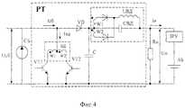
На фиг. 4 приведена схема силового модуля РТ с вольтодобавочным устройством, из которой видно, что организация вольтодобавочного устройства не требует дополнительного введения силовых транзисторов, поскольку в прототипе для повышения надежности изделия они всегда выполняются резервированными, а энергию для работы вольтодобавочное устройство получает непосредственно от самой СБ и преобразовывает часть мощности СБ в напряжение вольтодобавки Uвд, за счет организации двухтактного режима работы силовых транзисторов VT1 и VT2, подключенных к силовому трансформатору. При этом величину вольтодобавки Uвд можно изменять за счет изменения скважности q при управлении силовыми транзисторами, т.е. реализовать режим ШИМ ВД.In FIG. Figure 4 shows a diagram of the RT power module with a booster device, which shows that the organization of a booster device does not require the introduction of additional power transistors, since in the prototype to increase the reliability of the product they are always made redundant, and the booster device receives energy for operation directly from the SB itself and converts part of the power of the SB in the voltage boost Uvd , due to the organization of a push-pull operation mode of power transistors VT1 and VT2 connected to the forces ohm transformer. In this case, the magnitude of the voltage boost Uvd can be changed due to a change in the duty cycle q when controlling power transistors, i.e. implement PWM VD mode.
Таким образом, в РТ реализуется четвертый режим работы (режим ВД) и происходит следующее:
1) От деградированной СБ при наличии напряжения вольтодобавки Uвд в режиме ШИМ (при q=1), отбирается ток IГ, соответствующий оптимальной точке Г на фиг. 1, кривая 3, и напряжение СБ всегда равно Ucб=Uн-Uвд, а РГ=РБ-Рвд, где Рвд - потери в преобразователе вольтодобавки.Thus, the fourth mode of operation (VD mode) is implemented in RT and the following occurs:
1) From Sa degraded in the presence of the boost voltage Uvd in PWM mode (when q = 1) is shown the current ID corresponding to the optimum point F in FIGS. 1, curve 3, and the SB voltage is always equal to Ucb = Un -Uvd , and PG = PB -Pvd , where Pvd is the loss in the boost converter.
2) При закрытых транзисторах VT1 и VT2 (см. фиг.4), в паузе, в режиме ШИМ ВД ток нагрузки Iн=Iсб=IБ (см. точку Б фиг.1, кривая 2), а напряжение вольтодобавки Uвд поддерживается фильтром Lвд Свд (см. фиг.5) за счет накопленной энергии.2) With the closed transistors VT1 and VT2 (see figure 4), in a pause, in the PWM VD mode, the load current is In = Isat = IB (see point B of figure 1, curve 2), and the voltage boost Uvd is supported by the filter Lvd Cvd (see Fig. 5) due to the accumulated energy.
3) При открытом одном из транзисторов (при 0<q<1, в) от СБ отбирается тот же ток Iсб, соответствующий точке Б на фиг.1, кривая 2, а ток нагрузки Iн уменьшается на величину тока преобразователя вольтодобавки Iвд=Iн•Ктр, (Ктр= W2/W1), так как этот ток используется для заряда Свд, и равен IГ на фиг. 1, кривая 2. Следовательно, через диод VD протекает пульсирующий ток, равный ΔI = Iн-Iвд. Эта пульсирующая составляющая тока нагрузки сглаживается конденсатором С (см. фиг.4).3) When one of the transistors is open (for 0 <q <1, c), the same current Isb , corresponding to point B in Fig. 1,
4) При q=0, напряжение вольтодобавки Uвд=0 и при подаче синфазных сигналов в базы силовых транзисторов, регулирование мощности СБ (при ее избытке) будет осуществляться за счет изменения длительности открытого состояния обоих транзисторов и схема РТ становится эквивалентной фиг.2, при этом первичные обмотки трансформатора вольтодобавки будут закорочены транзисторами VT1, VT2 и вольтодобавочное устройство не оказывает влияния на работу РТ.4) When q = 0, the voltage boostUd = 0 and when common-mode signals are supplied to the base of power transistors, the SB power control (if there is an excess of it) will be carried out by changing the duration of the open state of both transistors and the RT circuit becomes equivalent to Fig. 2, the primary windings of the boost transformer will be shorted by transistors VT1, VT2 and the boost device does not affect the operation of the RT.
5) При дискретной установке величины вольтодобавки Uвд и несанкционированном частичном отключении нагрузки возможно увеличение выходного напряжения Uрт>Uн.5) With a discrete installation of the voltage boost value Uvd and unauthorized partial disconnection of the load, an increase in the output voltage Urt > Un is possible.
Для предотвращения указанного режима в устройстве реализован пятый режим работы ШИМ РТ + ШИМ ВД, т.е. первый и четвертый режим одновременно, при котором в любых нештатных ситуациях Uн будет всегда стабильным на шинах для подключения нагрузки и АБ.To prevent this mode, the device implements the fifth mode of operation of the PWM RT + PWM VD, i.e. the first and fourth mode at the same time, in which in any emergency situations Un will always be stable on the buses for connecting the load and battery.
6) С учетом того, что потери на введение ВД не превышают 2% от Popt=РБ в деградированной СБ, то предлагаемый способ отбора мощности от СБ позволяет существенно повысить эффективность использования СБ в СЭС.6) Taking into account the fact that the losses on the introduction of airborne weapons do not exceed 2% of Popt =RB in a degraded SB, the proposed method of power take-off from a SB allows to significantly increase the efficiency of using a SB in a SES.
На фиг.5 представлена схема устройства регулирования избыточной мощности с вольтодобавочным устройством, на фиг.6 представлены временные диаграммы, поясняющие работу вольтодобавочного устройства в режиме трансляции при деградированной СБ. Figure 5 presents a diagram of a device for regulating excess power with a booster device, Fig.6 presents time charts explaining the operation of a booster device in broadcast mode with degraded SB.
На фиг.7 представлены временные диаграммы работы устройства с вольтодобавкой в режиме ШИМ РТ + ШИМ ВД. Figure 7 presents the timing diagrams of the operation of the device with voltage boost in the PWM RT + PWM VD mode.
Устройство содержит клеммы для подключения солнечной батареи (СБ) 1, отрицательный вывод которой подключен к общей минусовой шине устройства, силовые транзисторы 2 и 6, коллекторы которых соединены с первичными обмотками силового трансформатора 3 и 5 соответственно, а их эммитеры подключены к общей минусовой шине, предохранитель 4, включенный между плюсовой шиной СБ и общей точкой соединения обмоток 3 и 5 силового трансформатора, разделительный диод 7, анод которого подключен к плюсовой шине СБ, а катод - к общей точке соединения вторичных обмоток 11 и 12 силового трансформатора, другие выводы которых соединены с анодами выпрямительных диодов 13 и 14 соответственно, соединенные вместе катоды диодов 13 и 14 подключены к первому выводу дросселя 16, а его второй вывод соединен с плюсовой выходной шиной для подключения нагрузки, вольтодобавочный конденсатор 15, включенный между общей точкой соединения обмоток 11, 12 и плюсовой выходной шиной, конденсатор 8 и первый резистивный делитель из резисторов 9, 10, подключенный между катодом разделительного диода 7 и общей минусовой шиной, второй резистивный делитель из резисторов 17, 18, подключенный между выходными шинами устройства, к которым подключена нагрузка 19. The device contains terminals for connecting a solar battery (SB) 1, the negative terminal of which is connected to the common negative bus of the device,
Схема управления содержит первый усилитель рассогласования 20, подключенный к положительной шине устройства и предназначенный для сравнения выходного, напряжения нагрузки с опорным напряжением упомянутого усилителя рассогласования, широтно-импульсный регулятор 21, в который входят генератор импульсов 22 (ГИ), генератор пилообразного напряжения 23 (ГПН) и первый компаратор 24, на инвертирующий вход которого поступает пилообразное напряжение с ГПН 23, а на неинвертирующий вход поступает напряжение с усилителя рассогласования 20, при этом выход первого компаратора 24 соединен со вторыми входами элементов И-НЕ 31 и 32, входы датчика напряжения (ДН) 25 подключены к средним точкам первого (9, 10) и второго (17, 18) резистивных делителей, а его выход - к инвертирующему входу второго усилителя рассогласования 27, неинвертирующий вход которого подключен к выходу формирователя опорных напряжений 26, на вход которого подается команда "Установка U-ВД". Выход второго усилителя рассогласования 27 соединен с неинвертирующим входом второго компаратора 28, инвертирующий вход которого соединен с выходом ГПН 23. Фазорасщепитель 29 состоит из триггера 30 и элементов И-НЕ 31, 32, при этом на синхровход триггера 30 поступают импульсы с ГИ 22, а выходы триггера 30 соединены с третьими входами элементов И-НЕ 31, 32, первые входы которых соединены с выходом второго компаратора 28, а вторые входы элементов И-НЕ 31, 32 подключены к клемме, через которую в устройство подается команда "Вкл. ВД". The control circuit includes a
Первые входы элементов И-НЕ 33, 34 соединены с выходами элементов И-НЕ 31, 32 соответственно, а вторые входы соединены с выходом первого компаратора 24. Выходы элементов И-НЕ 33, 34 через предварительные усилители 35 и 36 соединены с базами силовых транзисторов 6 и 2 соответственно. The first inputs of the AND-
Устройство работает следующим образом. При недостатке мощности у деградированной СБ РТ работает в режиме 3 (трансляция) и рабочая точка СБ находится в точке В на фиг.1, кривая 2. При этом силовые транзисторы закрыты, т. к. Uн на входе первого усилителя рассогласования 20 будет несколько ниже опорного напряжения указанного усилителя, и на его выходе установится сигнал с положительным уровнем напряжения, превышающим амплитуду пилообразного напряжения, которое вырабатывается генератором пилообразного напряжения (ГПН) 23 (см.фиг.6 в) из импульсной последовательности, которую формирует генератор импульсов (ГИ) 22 (см.фиг.6 б), и на выходе первого компаратора 24 установится сигнал с положительным логическим уровнем "1", который поступит на вторые выходы элементов И-НЕ 33, 34, тем самым разрешая прохождение сигналов управления на силовые транзисторы с ШИМ ВД, которое осуществляется командой вольтодобавочного устройства. Включение устройства в режим ШИМ ВД осуществляется командой Вкл. ВД с логическим уровнем "1" (см.фиг.6 а), которая поступает на вторые входы элементов И-НЕ 31, 32 фазорасщепителя 29, при этом на третьих входах указанных элементов 31, 32 всегда присутствуют импульсы, сдвинутые по фазе и поступающие с выхода триггера 30 фазорасщепителя 29 (см. фиг.6 г, д), которые формируются из импульсов ГИ 22 (см.фиг.6 б).The device operates as follows. With a lack of power in a degraded SB, the RT operates in mode 3 (broadcast) and the SB operating point is at point B in Fig. 1,
В исходном состоянии, когда команда Вкл. ВД установлена, а на входе формирователя опорных напряжений (ФОН) 26 отсутствует команда "Установка U-ВД", на выходе второго компаратора 28 присутствует напряжение с уровнем логического нуля "0", который через первые входы элементов И-НЕ 31, 32 установит на первых входах элементов И-НЕ 33, 34 сигнал с уровнем логической "1", и, в связи с тем, что на вторых входах И-НЕ 33, 34 установлено напряжение, равное "1", с первого компаратора 24, сигнал с уровнем логического нуля "0" с выходов И-НЕ 33, 34 через предварительные усилители 35, 36 поступит на базы силовых транзисторов 6 и 2, удерживая их в закрытом состоянии. In the initial state, when the command is On. The VD is installed, and the “U-VD Installation” command is absent at the input of the reference voltage driver (BACKGROUND) 26; at the output of the
При появлении импульса управления "Установка U-ВД" на входе ФОН 26, на его выходе сформируется опорное напряжение, соответствующее установке 1-го уровня напряжения U-ВД, которое, совместно с напряжением ГПН (см.фиг.6 в) сформирует на выходе второго компаратора 28 импульсы ШИМ ВД (фиг.6 ж), эти импульсы с помощью фазорасщепителя 29 через элементы И-НЕ 33, 34 и предварительные усилители 35, 36 поступят на базы силовых транзисторов 6 и 2, которые начнут работать в двухтактном режиме (см. фиг.6 и к, л, м), вследствие чего на вторичных обмотках 11, 12 силового трансформатора появится напряжение, которое через выпрямительные диоды 13, 14 и дроссель 16 зарядит вольтодобавочный конденсатор 15. When the "U-VD Installation" control pulse appears at the
Напряжение со средних точек первого 9, 10 и второго 17, 18 резистивных делителей, представляющих собой напряжение обратной связи, через датчик напряжения 25 поступает на инвертирующий вход второго усилителя рассогласования 27 и, тем самым, поддерживает напряжение Uвд стабильным. The voltage from the midpoints of the first 9, 10 and second 17, 18 resistive dividers, which is a feedback voltage, is supplied through the voltage sensor 25 to the inverting input of the second mismatch amplifier 27 and, thus, keeps the voltage Uvd stable.
Т. о. , с приходом очередного импульса команды "Установка U-ВД" можно, увеличивая напряжение вольтодобавки, смещать рабочую точку СБ из точки В (см. фиг.1, кривая 2) в точку Б, в которой мощность СБ будет иметь экстремальное значение. T. about. , with the arrival of the next impulse of the U-VD Installation command, it is possible, by increasing the voltage boost voltage, to shift the SB operating point from point B (see Fig. 1, curve 2) to point B, in which the SB power will have an extreme value.
При превышении выходного напряжения РТ выше значения Uн одновременно с режимом ШИМ РТ реализуется режим ШИМ ВД, так как начинает работать широтно-импульсный регулятор 21, напряжение на инвертирующем входе первого усилителя рассогласования 20 Uн станет несколько выше опорного напряжения указанного усилителя, за счет чего на выходе первого компаратора 24 появляются импульсы (см. фиг.7 в, е), длительность которых, изменяясь в функции выходного напряжения РТ, стабилизирует его с использованием широтно-импульсной модуляции.If the output voltage of the RT exceeds the value of Un simultaneously with the PWM mode of the RT, the PWM VD mode is implemented, since the pulse-
Т. о., реализуется 1-й режим работы РТ (ШИМ РТ), при котором на базы силовых транзисторов поступают синфазные сигналы управления Uбэ1 и Uбэ2 (см. фиг. 7 и, к), в результате чего происходит регулирование избыточной мощности СБ путем ее закорачивания на силовые транзисторные ключи 2, 6.Thus, the 1st mode of operation of the RT (PWM RT) is implemented, in which in-phase
Указанные режимы ШИМ РТ и ШИМ ВД реализуются совместно, но не оказывают влияние друг на друга за счет того, что импульсы управления, поступающие на транзисторы 2 и 6, сдвинуты по фазе на полупериод. Например, когда осуществляется двухтактный режим работы преобразователя вольтодобавки в момент t1 на фиг. 7 и, к, л, м, открыт транзистор 2, а транзистор 6 закрыт, поэтому силовой трансформатор намагничивается, допустим, в прямом направлении. The indicated PWM RT and PWM VD modes are implemented jointly, but do not affect each other due to the fact that the control pulses arriving at
В следующий полупериод (в момент t2-t4 на фиг.7 и-м) широтно-импульсный регулятор 21 вырабатывает синфазные импульсы управления транзисторами 2 и 6, поэтому они закорачивают СБ. В момент t5-t6 откроется транзистор 6, перемагничивая силовой трансформатор вольтодобавки в обратном направлении. А в течение следующего полупериода в момент t7-t8 широтно-импульсный регулятор 21 вырабатывает синфазные сигналы, открывающие транзисторы 2 и 6, закорачивая СБ. Поскольку ШИМ РТ (синфазное управление транзисторами 2, 6) всегда превалирует над режимом ШИМ ВД, транзисторы работают в двухтактном режиме, и в этом случае выходное напряжение РТ Uн будет всегда оставаться стабильным.In the next half-cycle (at time t2-t4 in Fig. 7 i-m), the pulse-
Предлагаемое изобретение позволяет организовать отбор максимальной мощности от деградированной солнечной батареи (СБ) без применения специальных экстрематоров путем введения в устройство для регулирования избыточной мощности СБ вольтодобавочного устройства, которое получает энергию от самой СБ, и за счет дискретного изменения напряжения вольтодобавки, а также позволяет перемещать рабочую точку СБ в область максимально отдаваемой мощности, что существенно повышает эффективность использования солнечной батареи. The present invention allows to organize the selection of maximum power from a degraded solar battery (SB) without the use of special extremators by introducing into the device for controlling the excess power of the SB a booster device that receives energy from the SB itself and due to a discrete change in the voltage of the booster, and also allows you to move the working point SB in the area of maximum power output, which significantly increases the efficiency of use of the solar battery.
Источники информации
1. РТ-50 по ЕИГА.435264.001-03.Sources of information
1. RT-50 according to EIGA.435264.001-03.
Claims (1)
Translated fromRussianPriority Applications (1)
| Application Number | Priority Date | Filing Date | Title |
|---|---|---|---|
| RU2001111490/09ARU2211480C2 (en) | 2001-04-25 | 2001-04-25 | Device for controlling solar-battery excess power |
Applications Claiming Priority (1)
| Application Number | Priority Date | Filing Date | Title |
|---|---|---|---|
| RU2001111490/09ARU2211480C2 (en) | 2001-04-25 | 2001-04-25 | Device for controlling solar-battery excess power |
Publications (2)
| Publication Number | Publication Date |
|---|---|
| RU2001111490A RU2001111490A (en) | 2003-04-20 |
| RU2211480C2true RU2211480C2 (en) | 2003-08-27 |
Family
ID=29245428
Family Applications (1)
| Application Number | Title | Priority Date | Filing Date |
|---|---|---|---|
| RU2001111490/09ARU2211480C2 (en) | 2001-04-25 | 2001-04-25 | Device for controlling solar-battery excess power |
Country Status (1)
| Country | Link |
|---|---|
| RU (1) | RU2211480C2 (en) |
Cited By (3)
| Publication number | Priority date | Publication date | Assignee | Title |
|---|---|---|---|---|
| US9780564B2 (en) | 2012-09-28 | 2017-10-03 | Eaton Corporation | Dual-input inverter and method of controlling same |
| RU2693020C1 (en)* | 2018-10-11 | 2019-07-01 | Федеральное государственное унитарное предприятие "Центральный ордена Трудового Красного Знамени научно-исследовательский автомобильный и автомоторный институт "НАМИ" (ФГУП "НАМИ") | Photoelectrical solar energy conversion device |
| RU2838511C1 (en)* | 2024-09-02 | 2025-04-17 | Федеральное государственное унитарное предприятие "Центральный ордена Трудового Красного Знамени научно-исследовательский автомобильный и автомоторный институт "НАМИ" (ФГУП "НАМИ") | Device for providing maximum energy output of photoelectric converter (pec) module |
Citations (4)
| Publication number | Priority date | Publication date | Assignee | Title |
|---|---|---|---|---|
| SU1495770A1 (en)* | 1985-12-23 | 1989-07-23 | Куйбышевский институт инженеров железнодорожного транспорта | Method for pulsed stabilizer control |
| US4899269A (en)* | 1988-01-29 | 1990-02-06 | Centre National D'etudes Spatiales | System for regulating the operating point of a direct current power supply |
| DE4328511A1 (en)* | 1993-08-25 | 1995-03-09 | Zsw | Turn-on control method and turn-on control circuit for an invertor coupling a solar generator to the electricity mains |
| FR2766589A1 (en)* | 1997-07-28 | 1999-01-29 | Centre Nat Etd Spatiales | DEVICE FOR CONTROLLING THE OPERATION POINT OF AN ELECTRIC POWER GENERATOR, PARTICULARLY A SOLAR GENERATOR |
- 2001
- 2001-04-25RURU2001111490/09Apatent/RU2211480C2/enactiveIP Right Revival
Patent Citations (4)
| Publication number | Priority date | Publication date | Assignee | Title |
|---|---|---|---|---|
| SU1495770A1 (en)* | 1985-12-23 | 1989-07-23 | Куйбышевский институт инженеров железнодорожного транспорта | Method for pulsed stabilizer control |
| US4899269A (en)* | 1988-01-29 | 1990-02-06 | Centre National D'etudes Spatiales | System for regulating the operating point of a direct current power supply |
| DE4328511A1 (en)* | 1993-08-25 | 1995-03-09 | Zsw | Turn-on control method and turn-on control circuit for an invertor coupling a solar generator to the electricity mains |
| FR2766589A1 (en)* | 1997-07-28 | 1999-01-29 | Centre Nat Etd Spatiales | DEVICE FOR CONTROLLING THE OPERATION POINT OF AN ELECTRIC POWER GENERATOR, PARTICULARLY A SOLAR GENERATOR |
Cited By (3)
| Publication number | Priority date | Publication date | Assignee | Title |
|---|---|---|---|---|
| US9780564B2 (en) | 2012-09-28 | 2017-10-03 | Eaton Corporation | Dual-input inverter and method of controlling same |
| RU2693020C1 (en)* | 2018-10-11 | 2019-07-01 | Федеральное государственное унитарное предприятие "Центральный ордена Трудового Красного Знамени научно-исследовательский автомобильный и автомоторный институт "НАМИ" (ФГУП "НАМИ") | Photoelectrical solar energy conversion device |
| RU2838511C1 (en)* | 2024-09-02 | 2025-04-17 | Федеральное государственное унитарное предприятие "Центральный ордена Трудового Красного Знамени научно-исследовательский автомобильный и автомоторный институт "НАМИ" (ФГУП "НАМИ") | Device for providing maximum energy output of photoelectric converter (pec) module |
Similar Documents
| Publication | Publication Date | Title |
|---|---|---|
| US7227277B2 (en) | Multiple input DC-DC power converter | |
| US5583753A (en) | Parallel control type DC--DC converter | |
| JP3175121B2 (en) | Uninterruptible power system | |
| US7982434B2 (en) | Apparatus and method for controlling a power supply | |
| US8981738B2 (en) | Solar array regulator based on step-up and down conversion and solar power system comprising the same | |
| US7009859B2 (en) | Dual input DC-DC power converter integrating high/low voltage sources | |
| US4851756A (en) | Primary-secondary hybrid battery | |
| CN112928800B (en) | Charging circuit and charging system | |
| CN101841242B (en) | Switch power supply and method for adjusting output current thereof | |
| WO2013061461A1 (en) | Battery system | |
| US10186861B2 (en) | Energy storage device comprising a DC voltage supply circuit and method for providing a DC voltage from an energy storage device | |
| US20050112420A1 (en) | Power supply device | |
| CN103219910A (en) | Power converter circuit | |
| US20190379271A1 (en) | Multi-input single-output dc-dc converter, control circuit and control method thereof | |
| US20200144956A1 (en) | Photovoltaic system | |
| US5397976A (en) | Control system for voltage controlled bilateral current source | |
| EP4125201A1 (en) | Three-level direct current converter, power supply system, and chip | |
| US6617831B2 (en) | Electrical power supply converter | |
| Middlebrook et al. | A new battery charger/discharger converter | |
| CN119765850A (en) | DC/DC converter, energy storage system and optical storage system | |
| RU2211480C2 (en) | Device for controlling solar-battery excess power | |
| CN112242697A (en) | High-power SAR satellite power supply equalizing system | |
| Schulz et al. | Four Switch Buck/Boost Converter to Handle Bidirectional Power Flow in DC Subgrids | |
| CN213846540U (en) | Auxiliary power supply circuit, driver and wind power generation system | |
| JP2789778B2 (en) | Power supply |
Legal Events
| Date | Code | Title | Description |
|---|---|---|---|
| PC4A | Invention patent assignment | Effective date:20060704 | |
| MM4A | The patent is invalid due to non-payment of fees | Effective date:20100426 | |
| NF4A | Reinstatement of patent | Effective date:20120827 |