RU2209471C2 - Ac color gas panel - Google Patents
Ac color gas panelDownload PDFInfo
- Publication number
- RU2209471C2 RU2209471C2RU2001122678ARU2001122678ARU2209471C2RU 2209471 C2RU2209471 C2RU 2209471C2RU 2001122678 ARU2001122678 ARU 2001122678ARU 2001122678 ARU2001122678 ARU 2001122678ARU 2209471 C2RU2209471 C2RU 2209471C2
- Authority
- RU
- Russia
- Prior art keywords
- electrodes
- display
- discharge
- dielectric
- control
- Prior art date
Links
- 230000004888barrier functionEffects0.000claimsabstractdescription23
- OAICVXFJPJFONN-UHFFFAOYSA-NPhosphorusChemical compound[P]OAICVXFJPJFONN-UHFFFAOYSA-N0.000claimsabstractdescription8
- 239000004020conductorSubstances0.000claimsdescription22
- 239000011159matrix materialSubstances0.000claimsdescription10
- 239000000463materialSubstances0.000claimsdescription7
- 238000004020luminiscence typeMethods0.000claimsdescription2
- 239000012780transparent materialSubstances0.000claimsdescription2
- 241000272517AnseriformesSpecies0.000claims1
- 239000003086colorantSubstances0.000claims1
- 238000000034methodMethods0.000abstractdescription7
- 238000002360preparation methodMethods0.000abstractdescription3
- 238000000926separation methodMethods0.000abstractdescription3
- 230000001678irradiating effectEffects0.000abstractdescription2
- 230000005855radiationEffects0.000abstractdescription2
- 230000000694effectsEffects0.000abstract1
- 239000000126substanceSubstances0.000abstract1
- 239000011521glassSubstances0.000description4
- 238000009825accumulationMethods0.000description2
- 230000015572biosynthetic processEffects0.000description2
- 239000000203mixtureSubstances0.000description2
- 238000004458analytical methodMethods0.000description1
- 238000004364calculation methodMethods0.000description1
- 230000015556catabolic processEffects0.000description1
- 238000006731degradation reactionMethods0.000description1
- 238000005516engineering processMethods0.000description1
- -1phosphor ionsChemical class0.000description1
- 230000006641stabilisationEffects0.000description1
- 238000011105stabilizationMethods0.000description1
- 230000000087stabilizing effectEffects0.000description1
- 230000007704transitionEffects0.000description1
Images


Landscapes
- Control Of Indicators Other Than Cathode Ray Tubes (AREA)
- Gas-Filled Discharge Tubes (AREA)
Abstract
Description
Translated fromRussianИзобретение относится к области техники индикации и может быть использовано при разработке средств отображения, созданных на цветных плазменных панелях (ПП) переменного тока. The invention relates to the field of indication technology and can be used to develop display means created on color plasma panels (PP) of alternating current.
Известна панель переменного тока; содержащая две стеклянных пластины, и на поверхности тыльной стороны пластины находятся электроды строк, покрытые прозрачным диэлектриком, а на лицевой стороне пластины расположены электроды столбцов, пространственное пересечение этих электродов образует ячейки индикации; и каждый увеличенный в размерах элемент отображения состоит из группы ячеек индикации (патент Франции 2641413, кл. H 01 J 17/49 от 08.06.1990). Основной недостаток данной ПП в том, что конструкция ячеек индикации не позволяет использовать люминофоры для получения цвета из-за бомбардировки ионами люминофора, что приводит к деградации люминофора, а в панели отсутствуют условия повышения контраста отображаемой информации. Known AC panel; containing two glass plates, and on the surface of the back side of the plate are row electrodes coated with a transparent dielectric, and column electrodes are located on the front side of the plate, the spatial intersection of these electrodes forms display cells; and each enlarged display element consists of a group of display cells (French patent 2641413, CL H 01
Известна ПП переменного тока с поверхностным разрядом, каждый элемент отображения которой содержит два индикаторных разрядных промежутка, образованных петлеобразными электродами индикации, управляющий электрод с диэлектрическими барьерами и люминофор (патент US 5852347, кл. G 09 F 9/00 от 22.12.1998). Known AC AC with a surface discharge, each display element of which contains two indicator discharge gaps formed by loop-shaped indication electrodes, a control electrode with dielectric barriers and a phosphor (patent US 5852347, CL G 09 F 9/00 from 12/22/1998).
К причинам, препятствующим достижению требуемого технического результата при использовании известной конструкции панели относится то, что в известной панели отсутствуют условия повышения контраста, поскольку разряд в режиме подготовки происходит между электродами индикации, а фоновая подсветка охватывает всю площадь элемента отображения и соответственно всю площадь пикселя. Наиболее близкой к предлагаемой конструкции ПП является ПП переменного тока с поверхностным разрядом, содержащая в каждом пикселе три элемента отображения с разным цветом свечения люминофора, которые располагаются вдоль управляющих электродов. Элементы отображения отделяются друг от друга барьерами матрицы диэлектрической решетки, и в каждом элементе отображения индикаторный разрядный промежуток образован двумя параллельными электродами индикации, один из которых сканирующий электрод, который вместе с перпендикулярным им управляющим электродом, образуют управляющий разрядный промежуток (патент US 6088010, кл. G 09 G 3/28 от 11.07.2000). К причинам, препятствующим достижению требуемого технического результата при использовании известной плазменной панели, относится то, что увеличение размера ячейки индикации за счет простого увеличения длины электродов индикации приводит к неполному охвату свечения разряда вдоль электродов индикации из-за ограниченной скорости распространения разряда по катоду во время ввода информации и индикации. Внешне это проявляется как мерцание отдельных пикселей, которые ухудшают качество отображаемой информации, и отсутствуют условия повышения контраста отображаемой информации. The reasons that impede the achievement of the required technical result when using the known panel design include the fact that the known panel has no conditions for increasing contrast, since the discharge in the preparation mode occurs between the display electrodes, and the backlight covers the entire area of the display element and, accordingly, the entire area of the pixel. Closest to the proposed PP design is an alternating current PP with a surface discharge, containing in each pixel three display elements with a different color of the phosphor glow, which are located along the control electrodes. The display elements are separated from each other by the barriers of the dielectric array matrix, and in each display element the indicator discharge gap is formed by two parallel indication electrodes, one of which is a scanning electrode, which together with a control electrode perpendicular to it, form a control discharge gap (patent US 6088010, cl. G 09
Задача изобретения состоит в создании цветной плазменной панели переменного тока с элементами отображения увеличенных размеров с повышенной надежностью работы и управления и высоким контрастом отображаемой информации. Технический результат - повышение надежности работы и управления - достигается за счет деления электродов индикации на отдельные индикаторные разрядные промежутки в каждом элементе отображения. Выполнение сканирующего электрода индикации в виде двух проводников, что в совокупности позволяет стабилизировать процесс возникновения разряда во время ввода информации и индикации ее. Увеличенный контраст отображаемой информации получается за счет дополнительного разрядного промежутка между проводниками сканирующего электрода индикации, в котором осуществляется режим подготовки разряда. Свечение фона этого режима охватывает небольшую часть площади элемента отображения и соответственно площадь пикселя. Дополнительное увеличение контраста происходит, когда в каждом элементе отображения дополнительные разрядные промежутки закрыты светонепроницаемым материалом. Указанный технический результат при осуществлении изобретения достигается тем, что в известной цветной плазменной панели переменного тока с поверхностным разрядом, содержащей в каждом пикселе три элемента отображения с разным цветом свечения люминофора, располагаются вдоль управляющих электродов, и элементы отображения отделяются друг от друга барьерами матрицы диэлектрической решетки, и в каждом элементе отображения индикаторный разрядный промежуток образован двумя параллельными электродами индикации. Один из них - сканирующий электрод, который вместе с перпендикулярным им управляющим электродом образуют управляющий разрядный промежуток, в каждом элементе отображения электроды индикации разделены на отдельные индикаторные промежутки перпендикулярными к электродам индикации диэлектрическими барьерами, высота которых выбрана из соотношения h = (0,1-0,9)d, где h - высота диэлектрического барьера, d - толщина барьеров матрицы диэлектрической решетки. В каждом отдельном индикаторном разрядном промежутке сканирующий электрод выполнен из двух проводников, между проводниками образован дополнительный разрядный промежуток, в котором разрядный промежуток управления сформирован параллельными проводниками управляющего электрода и крайним проводником сканирующего электрода элемента отображения. При этом проводник управляющего электрода соединен с шиной и расположен пространственно-перпендикулярно относительно электродов индикации и проходит через один из отдельных индикаторных разрядных промежутков. Разделительные диэлектрические барьеры выполнены из прозрачного материала, шины проводников управляющего электрода проходят между пикселями под барьерами диэлектрической матрицы, промежуток между проводниками сканирующего электрода закрыт светонепроницаемым материалом. Разделение элемента отображения на отдельные индикаторные разрядные промежутки позволяет обеспечить оптимальную длину электродов индикации в соответствии со временем распространения разряда вдоль катода и процесса накопления зарядов на поверхности электродов индикации. Это стабилизирует возникновение поверхностных разрядов между электродами индикации во время ввода информации и индикации, что повышает надежность управления и работы ПП. Выбранная высота диэлектрических барьеров создает оптимальные условия облучения люминофора ультрафиолетовым излучением (УФИ) по всей поверхности элемента отображения от всех отдельных индикаторных разрядных промежутков. Применение сканирующего электрода индикации в виде двух проводников дает возможность создать дополнительный разрядный промежуток в каждом отдельном индикаторном разрядном промежутке элемента отображения с образованием разрядного промежутка управления газа между сканирующим и управляющим проводниками этих электродов, с увеличенным объемом ионизации газа. Увеличенный объем ионизации газа уменьшает время статистического запаздывания возникновения разряда во время адресации выбранного элемента отображения, что повышает надежность управления элементов отображения ПП при вводе информации. Использование прозрачных разделительных диэлектрических барьеров повышает яркость свечения элементов отображения и вместе с закрытием промежутка между проводниками сканирующего электрода светонепроницаемым материалом увеличивает контраст отображаемой информации. Расположение шин управляющих электродов между пикселями под барьерами диэлектрической матрицы устраняет электрическую связь этих электродов с электродами индикации, которая приводит к дестабилизации процесса накопления зарядов на поверхности этих электродов во время перехода от режима адресации к режиму индикации. Это повышает надежность работы ПП. Проведенный заявителем анализ уровня техники, включающий поиск по патентным и научно-техническим источникам информации, выявление источников, содержащих сведения об аналогах заявленного изобретения, позволяет установить, что заявителем не обнаружен аналог, характеризующийся признаками, идентичными признакам заявленного изобретения, и определение из перечня выявленных аналогов прототипа как наиболее близкого по совокупности признаков аналога позволило выявить совокупность существенных по отношению к усматриваемому заявителем техническому результату отличительных признаков в заявленном объекте, изложенных в формуле изобретения. Для проверки соответствия заявленного изобретения требованию изобретательского уровня был проведен дополнительный поиск известных решений с целью выявления признаков, совпадающих с отличительными от прототипа заявленного изобретения, результаты которого показывают, что заявленное изобретение не следует для специалиста явным образом из известного уровня техники, так как не известны технические решения, в которых надежность работы и управления ПП достигается за счет образования отдельных индикаторных разрядных промежутков. Вместе с дополнительным разрядным промежутком и разрядным промежутком управления, который сформирован параллельными проводниками электрода, обеспечивая стабильный процесс возникновения разрядов во время ввода информации и индикации, расположение шин управляющих электродов под барьерами диэлектрической матрицы устраняло электрическую связь между управляющим электродом и электродом индикации. Кроме того, не выявлены технические решения, в которых повышение контраста осуществлялось за счет дополнительного разрядного промежутка в каждом отдельном индикаторном разрядном элементе отображения, с использованием прозрачных разделительных диэлектрических барьеров. The objective of the invention is to create a color plasma AC panel with display elements of oversized dimensions with increased reliability of operation and control and high contrast of the displayed information. The technical result - improving the reliability of operation and control - is achieved by dividing the display electrodes into separate indicator discharge gaps in each display element. The implementation of the scanning electrode indications in the form of two conductors, which together allows you to stabilize the process of occurrence of the discharge during the input of information and its indication. The increased contrast of the displayed information is obtained due to the additional discharge gap between the conductors of the scanning indication electrode, in which the discharge preparation mode is carried out. The background glow of this mode covers a small part of the area of the display element and, accordingly, the area of the pixel. An additional increase in contrast occurs when in each display element the additional discharge gaps are covered by opaque material. The specified technical result in the implementation of the invention is achieved by the fact that in the known color plasma AC panel with a surface discharge, containing in each pixel three display elements with a different color of the phosphor glow, are located along the control electrodes, and the display elements are separated from each other by the barriers of the dielectric array matrix , and in each display element, the indicator discharge gap is formed by two parallel indication electrodes. One of them is a scanning electrode, which together with a control electrode perpendicular to it forms a control discharge gap, in each display element, the indication electrodes are divided into separate indicator gaps by dielectric barriers perpendicular to the indication electrodes, the height of which is selected from the relation h = (0.1-0 , 9) d, where h is the height of the dielectric barrier, d is the thickness of the barriers of the dielectric array matrix. In each individual indicator discharge gap, the scanning electrode is made of two conductors, an additional discharge gap is formed between the conductors, in which the control discharge gap is formed by parallel conductors of the control electrode and the extreme conductor of the scanning electrode of the display element. In this case, the conductor of the control electrode is connected to the bus and is spatially perpendicular to the indication electrodes and passes through one of the individual indicator discharge gaps. Separating dielectric barriers are made of transparent material, the wires of the conductors of the control electrode pass between the pixels under the barriers of the dielectric matrix, the gap between the conductors of the scanning electrode is closed by an opaque material. Separation of the display element into separate indicator discharge gaps allows the optimal length of the indication electrodes to be provided in accordance with the time of discharge propagation along the cathode and the process of charge accumulation on the surface of the indication electrodes. This stabilizes the occurrence of surface discharges between the indication electrodes during the input of information and indication, which increases the reliability of control and operation of the PCB. The selected height of the dielectric barriers creates optimal conditions for irradiating the phosphor with ultraviolet radiation (UVI) over the entire surface of the display element from all individual indicator discharge gaps. The use of a scanning electrode of indication in the form of two conductors makes it possible to create an additional discharge gap in each individual indicator discharge gap of the display element with the formation of a discharge gap of gas control between the scanning and control conductors of these electrodes, with an increased volume of gas ionization. The increased volume of gas ionization reduces the statistical delay time of the occurrence of a discharge during the addressing of the selected display element, which increases the reliability of the control of the display elements of the PP when entering information. The use of transparent dividing dielectric barriers increases the brightness of the luminescence of the display elements and, together with closing the gap between the conductors of the scanning electrode with an opaque material, increases the contrast of the displayed information. The location of the busbars of the control electrodes between the pixels under the barriers of the dielectric matrix eliminates the electrical connection of these electrodes with the indication electrodes, which destabilizes the process of accumulation of charges on the surface of these electrodes during the transition from the addressing mode to the indication mode. This increases the reliability of the software. The analysis of the prior art by the applicant, including a search by patent and scientific and technical sources of information, identification of sources containing information about analogues of the claimed invention, allows us to establish that the applicant has not found an analogue characterized by features identical to those of the claimed invention, and determining from the list of identified analogues the prototype as the closest in the totality of the features of the analogue revealed a set of essential in relation to the applicant sees those the result of the distinguishing features in the claimed subject matter set forth in the claims. To verify the conformity of the claimed invention to the requirements of the inventive step, an additional search was carried out for known solutions in order to identify features that match the distinctive features of the prototype of the claimed invention, the results of which show that the claimed invention does not explicitly follow from the prior art, since the technical is not known solutions in which the reliability of the operation and control of the PP is achieved through the formation of separate indicator discharge gaps. Together with an additional discharge gap and a discharge control gap, which is formed by parallel conductors of the electrode, providing a stable process of the occurrence of discharges during the input of information and indication, the location of the busbars of the control electrodes under the barriers of the dielectric matrix eliminated the electrical connection between the control electrode and the indication electrode. In addition, no technical solutions were identified in which the contrast was increased due to an additional discharge gap in each individual indicator bit display element using transparent dividing dielectric barriers.
Предлагаемая конструкция ПП поясняется чертежами. The proposed design of the PP is illustrated by drawings.
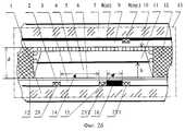
На фиг.1 схематически представлен разрез конструкции элемента отображения ПП с поверхностным разрядом, в котором электроды индикации разделены диэлектрическими барьерами на отдельные индикаторные разрядные промежутки. Figure 1 schematically shows a section of the design of the display element PP with a surface discharge, in which the display electrodes are separated by dielectric barriers into separate indicator discharge gaps.
На фиг.2а схематически представлен разрез конструкции элемента отображения, в котором сканирующий электрод состоит из двух проводников, образующих дополнительный разрядный промежуток, на фиг.2б представлен разрез, в котором дополнительный разрядный промежуток закрыт непрозрачным материалом. On figa schematically shows a section of the design of the display element, in which the scanning electrode consists of two conductors forming an additional discharge gap, figure 2B presents a section in which the additional discharge gap is closed by an opaque material.
На фиг. 3а схематически представлен цветной пиксель ПП, у которого шина управляющего электрода проходит в середине элемента отображения через отдельный индикаторный разрядный промежуток, а на фиг.3б - шина управляющего электрода проходит через крайний отдельный индикаторный разрядный промежуток элемента отображения. In FIG. 3a, a color pixel PP is schematically shown, in which the bus of the control electrode passes in the middle of the display element through a separate indicator bit gap, and in Fig. 3b, the bus of the control electrode passes through the extreme separate indicator bit gap of the display element.
На фиг.4 схематически представлена конструкция ПП с цветными пикселами, между которыми проходит шина управляющих электродов. Figure 4 schematically shows the design of the PP with color pixels, between which passes the bus of the control electrodes.
ПП (фиг.1-4) содержит лицевую стеклянную пластину 1 с электродами индикации 2, покрытые прозрачным диэлектриком 3, электроды индикации разделены диэлектрическими барьерами 4 на отдельные индикаторные разрядные промежутки 5, и в каждом отдельном индикаторном разрядном промежутке на поверхность прозрачного диэлектрика 3 нанесен стабилизирующий материал 6, тыльную стеклянную пластину 7 с управляющими электродами 8, состоящую из шины 8(ш.) и проводников 8(пр.), на которые нанесен диэлектрик 9 и люминофор 10. Зазор 11 между стеклянными пластинами 1 и 7 определяется толщиной матрицы диэлектрической решетки 12, элементы отображения 13 имеют в отдельных индикаторных разрядных промежутках 5 промежуток индикации 14 и дополнительный разрядный промежуток 15, закрытый непрозрачным материалом 16. Три элемента отображения красного цвета - 13R, зеленного цвета - 13G, синего цвета - 13В образуют цветной пиксель 17 ПП, в которой каждый элемент отображения 13 ограничен со всех сторон барьерами 18 матрицы диэлектрической решетки 12. ПП может иметь три варианта расположения шины 8(ш.) управляющего электрода 8, как это видно на фиг.1, 3, 4. PP (Figs. 1-4) contains a
Плазменная панель переменного тока с поверхностным разрядом работает следующим образом. На электроды индикации постоянно подаются импульсы напряжения поддержания разряда. Амплитуда напряжения этих импульсов не изменяет состояние элементов отображения. При адресации амплитуду импульсов напряжения поддержания разряда уменьшают; и для выборочного зажигания элементов отображения подают часть напряжения записи на выбранные управляющие электроды, а другую часть напряжения - на сканирующий электрод. В местах пересечения электродов (в зазоре) в дополнительном разрядном промежутке возникает разряд, подхватываемый затем в разрядном промежутке индикации между параллельными электродами при подаче импульсов напряжения поддержания разряда. При изменении информации в элементах отображения, в которых был разряд, после индикации осуществляют гашение разряда, а затем повторно проводят адресацию выбранных элементов отображения. A plasma discharge panel with a surface discharge operates as follows. The indication electrodes are constantly supplied with voltage pulses for maintaining the discharge. The voltage amplitude of these pulses does not change the state of the display elements. When addressing the amplitude of the pulses of the voltage to maintain the discharge is reduced; and for selective ignition of the display elements, a part of the recording voltage is supplied to the selected control electrodes, and another part of the voltage to the scanning electrode. At the points of intersection of the electrodes (in the gap) in the additional discharge gap, a discharge occurs, which is then picked up in the discharge gap of the indication between the parallel electrodes when applying voltage pulses to maintain the discharge. When information is changed in the display elements in which the discharge was, after the indication, the discharge is quenched, and then the selected display elements are addressed again.
Пример конкретного расчета элемента отображения для ПП с размером цветного пикселя 9 мм х 9 мм. Для этого пикселя размер элемента отображения будет 9 мм х 3 мм. При наполнении ПП газовой смесью Ne-Xe (4%) с давлением 500 тор для этой газовой смеси экспериментально определена скорость распространения разряда по катоду. Диапазон этой скорости находится в пределах (0,5-1,5) мм/мкс. Если не использовать разделение, то для длины электрода 9 мм при среднем значении скорости распространения разряда 1 мм/мкс величина длительности импульсов напряжения записи и импульса напряжения поддержания разряда будет около Т = 9 мкс. При такой длительности импульсов напряжения поддержания разряда нельзя получить в режиме индикации необходимую яркость изображения с градациями. Если элемент отображения разделить, например, на 3 отдельных индикаторных разрядных промежутка, то получим длину электродов около 3 мм, тогда длительность импульса напряжения будет 3 мкс. При индикации это позволяет получить необходимую яркость изображения, а при данном количестве индикаторных разрядных промежутков, при полученной длине электродов индикации с вышеуказанной скоростью распространения разряда будет обеспечена стабилизация процесса возникновения разрядов во время ввода информации и индикации. Это повысит надежность управления элементами отображения и работу панели в целом. На панели во время индикации элементы отображения будут гореть без мерцаний, что резко повышает качество отображаемой информации с градациями. An example of a specific calculation of a display element for PP with a color pixel size of 9 mm x 9 mm. For this pixel, the size of the display element will be 9 mm x 3 mm. When the PP was filled with a Ne-Xe gas mixture (4%) with a pressure of 500 torr, the velocity of discharge propagation through the cathode was experimentally determined for this gas mixture. The range of this speed is in the range (0.5-1.5) mm / μs. If separation is not used, then for an electrode length of 9 mm with an average value of the discharge propagation velocity of 1 mm / μs, the duration of the write voltage pulses and the discharge maintain voltage pulse will be about T = 9 μs. With such a pulse duration, the voltage for maintaining the discharge cannot be obtained in the display mode, the necessary image brightness with gradations. If the display element is divided, for example, into 3 separate indicator discharge gaps, then we obtain the length of the electrodes of about 3 mm, then the voltage pulse duration will be 3 μs. When indicating this, it is possible to obtain the necessary image brightness, and for a given number of indicator discharge gaps, with the obtained length of the indication electrodes with the above discharge propagation velocity, stabilization of the process of occurrence of discharges during information and indication input will be ensured. This will increase the reliability of control of display elements and the operation of the panel as a whole. On the panel during the display, the display elements will burn without flickering, which dramatically improves the quality of the displayed information with gradations.
Таким образом, вышеизложенные сведения свидетельствуют о выполнении при использовании заявленного изобретения следующей совокупности условий:
- средство, воплощающее заявленное изобретение при его осуществлении, предназначено для использования в промышленности, именно на базе цветной плазменной панели с элементами отображения увеличенных размеров возможно создание видеомодуля, из набора которых собирается экран коллективного пользования для отображения видеоинформации;
- для заявленного изобретения в том виде, как оно охарактеризовано в независимом пункте формулы изобретения, подтверждена возможность его осуществления с помощью вышеизложенных в заявке или известных до даты приоритета средств и методов;
- средство, воплощающее заявленное изобретение при его осуществлении, способно обеспечить достижение усматриваемого заявителем технического результата.Thus, the above information indicates the fulfillment of the following set of conditions when using the claimed invention:
- a tool embodying the claimed invention in its implementation is intended for use in industry, it is on the basis of a color plasma panel with enlarged display elements that it is possible to create a video module from which a collective screen for displaying video information is assembled;
- for the claimed invention in the form described in the independent claim, the possibility of its implementation using the means and methods described above or known prior to the priority date is confirmed;
- a tool embodying the claimed invention in its implementation, is able to ensure the achievement of the perceived by the applicant technical result.
Claims (3)
Translated fromRussian3. Цветная плазменная панель по п.1, отличающаяся тем, что шины проводников управляющего электрода выполнены между пикселями под барьерами диэлектрической матрицы.2. The color plasma panel according to claim 1, characterized in that the dividing dielectric barriers are made of a transparent material
3. The color plasma panel according to claim 1, characterized in that the busbars of the conductors of the control electrode are made between pixels under the barriers of the dielectric matrix.
Priority Applications (1)
| Application Number | Priority Date | Filing Date | Title |
|---|---|---|---|
| RU2001122678ARU2209471C2 (en) | 2001-08-14 | 2001-08-14 | Ac color gas panel |
Applications Claiming Priority (1)
| Application Number | Priority Date | Filing Date | Title |
|---|---|---|---|
| RU2001122678ARU2209471C2 (en) | 2001-08-14 | 2001-08-14 | Ac color gas panel |
Publications (2)
| Publication Number | Publication Date |
|---|---|
| RU2001122678A RU2001122678A (en) | 2003-06-27 |
| RU2209471C2true RU2209471C2 (en) | 2003-07-27 |
Family
ID=29210217
Family Applications (1)
| Application Number | Title | Priority Date | Filing Date |
|---|---|---|---|
| RU2001122678ARU2209471C2 (en) | 2001-08-14 | 2001-08-14 | Ac color gas panel |
Country Status (1)
| Country | Link |
|---|---|
| RU (1) | RU2209471C2 (en) |
Cited By (1)
| Publication number | Priority date | Publication date | Assignee | Title |
|---|---|---|---|---|
| RU2426177C2 (en)* | 2008-03-17 | 2011-08-10 | Общество с ограниченной ответственностью "ДиС ПЛЮС" | Method for exciting luminophor and element of altenating current colour plasma panel |
Citations (4)
| Publication number | Priority date | Publication date | Assignee | Title |
|---|---|---|---|---|
| SU1708092A1 (en)* | 1989-09-11 | 1996-05-10 | Научно-исследовательский институт знакосинтезирующей электроники "Волга" | Matrix self-emitting cathode |
| EP0837442A1 (en)* | 1996-10-21 | 1998-04-22 | Nec Corporation | Color plasma display panel and method of driving the same |
| RU2119206C1 (en)* | 1997-03-28 | 1998-09-20 | Совместное закрытое акционерное общество "Научно-производственная компания "ОРИОН-ПЛАЗМА" | Gaseous-discharge a c indicating panel |
| US5852347A (en)* | 1997-09-29 | 1998-12-22 | Matsushita Electric Industries | Large-area color AC plasma display employing dual discharge sites at each pixel site |
- 2001
- 2001-08-14RURU2001122678Apatent/RU2209471C2/ennot_activeIP Right Cessation
Patent Citations (4)
| Publication number | Priority date | Publication date | Assignee | Title |
|---|---|---|---|---|
| SU1708092A1 (en)* | 1989-09-11 | 1996-05-10 | Научно-исследовательский институт знакосинтезирующей электроники "Волга" | Matrix self-emitting cathode |
| EP0837442A1 (en)* | 1996-10-21 | 1998-04-22 | Nec Corporation | Color plasma display panel and method of driving the same |
| RU2119206C1 (en)* | 1997-03-28 | 1998-09-20 | Совместное закрытое акционерное общество "Научно-производственная компания "ОРИОН-ПЛАЗМА" | Gaseous-discharge a c indicating panel |
| US5852347A (en)* | 1997-09-29 | 1998-12-22 | Matsushita Electric Industries | Large-area color AC plasma display employing dual discharge sites at each pixel site |
Cited By (1)
| Publication number | Priority date | Publication date | Assignee | Title |
|---|---|---|---|---|
| RU2426177C2 (en)* | 2008-03-17 | 2011-08-10 | Общество с ограниченной ответственностью "ДиС ПЛЮС" | Method for exciting luminophor and element of altenating current colour plasma panel |
Similar Documents
| Publication | Publication Date | Title |
|---|---|---|
| KR100709935B1 (en) | Plasma display panel | |
| US8044888B2 (en) | Surface discharge type plasma display panel divided into a plurality of sub-screens | |
| US6034657A (en) | Plasma display panel | |
| EP0554172A1 (en) | Full color surface discharge type plasma display device | |
| US5789862A (en) | Surface discharge AC plasma display panel | |
| US6285128B1 (en) | Surface discharge type plasma display panel | |
| US7164394B2 (en) | Plasma display apparatus | |
| US6362799B1 (en) | Plasma display | |
| KR100679912B1 (en) | Plasma display device and driving method thereof | |
| JPH09259768A (en) | AC type PDP and driving method thereof | |
| RU2209471C2 (en) | Ac color gas panel | |
| RU2168790C2 (en) | Ac gas panel and its control process | |
| US7176852B2 (en) | Plasma display panel | |
| RU2158039C1 (en) | Gas-discharge alternating current indication board and method for its control | |
| RU2206924C2 (en) | Ac color gas panel with enlarged pixels | |
| RU2209472C2 (en) | Surface-discharge ac color gas panel | |
| KR100660249B1 (en) | Plasma display panel | |
| RU2216051C2 (en) | Surface-discharge ac plasma color panel | |
| KR19990065917A (en) | Plasma display | |
| RU2209473C2 (en) | Ac color gas panel for displaying video information | |
| RU2241276C2 (en) | Color plasma panel, method for controlling plasma panel, and display unit | |
| RU2216786C2 (en) | Ac color plasma panel | |
| RU2172039C2 (en) | Ac gas panel | |
| RU2214003C2 (en) | Surface-discharge plasma color panel for displaying video information | |
| RU2153729C1 (en) | Ac gas panel and its control process |
Legal Events
| Date | Code | Title | Description |
|---|---|---|---|
| MM4A | The patent is invalid due to non-payment of fees | Effective date:20130815 |