RU2172539C2 - Separable junction bridge (destructible jumper) and connectable open circuit (re-connectable jumper); method for manufacturing and activating destructible and re-connectable jumpers - Google Patents
Separable junction bridge (destructible jumper) and connectable open circuit (re-connectable jumper); method for manufacturing and activating destructible and re-connectable jumpersDownload PDFInfo
- Publication number
- RU2172539C2 RU2172539C2RU98116790ARU98116790ARU2172539C2RU 2172539 C2RU2172539 C2RU 2172539C2RU 98116790 ARU98116790 ARU 98116790ARU 98116790 ARU98116790 ARU 98116790ARU 2172539 C2RU2172539 C2RU 2172539C2
- Authority
- RU
- Russia
- Prior art keywords
- conductivity
- type
- conductor
- substrate
- current lead
- Prior art date
Links
- 238000004519manufacturing processMethods0.000titleclaimsabstractdescription10
- 238000000034methodMethods0.000titleclaimsdescription13
- 230000003213activating effectEffects0.000titleclaimsdescription10
- 238000009792diffusion processMethods0.000claimsabstractdescription68
- 239000004020conductorSubstances0.000claimsabstractdescription60
- 239000000758substrateSubstances0.000claimsabstractdescription48
- 239000000463materialSubstances0.000claimsabstractdescription44
- 239000004065semiconductorSubstances0.000claimsabstractdescription37
- 230000004913activationEffects0.000claimsabstractdescription35
- 238000010438heat treatmentMethods0.000claimsdescription29
- 239000012535impuritySubstances0.000claimsdescription27
- 230000005855radiationEffects0.000claimsdescription9
- 230000002427irreversible effectEffects0.000claimsdescription8
- 238000005275alloyingMethods0.000claimsdescription5
- 239000011247coating layerSubstances0.000claimsdescription5
- 238000002360preparation methodMethods0.000claimsdescription2
- 238000000926separation methodMethods0.000claims1
- 230000007704transitionEffects0.000claims1
- 239000000126substanceSubstances0.000abstract1
- 229910052751metalInorganic materials0.000description11
- 239000002184metalSubstances0.000description11
- 238000002513implantationMethods0.000description10
- 239000010410layerSubstances0.000description7
- ZOXJGFHDIHLPTG-UHFFFAOYSA-NBoronChemical compound[B]ZOXJGFHDIHLPTG-UHFFFAOYSA-N0.000description5
- 229910052796boronInorganic materials0.000description5
- XUIMIQQOPSSXEZ-UHFFFAOYSA-NSiliconChemical compound[Si]XUIMIQQOPSSXEZ-UHFFFAOYSA-N0.000description4
- 229910021420polycrystalline siliconInorganic materials0.000description4
- 229920005591polysiliconPolymers0.000description4
- 229910052710siliconInorganic materials0.000description4
- 239000010703siliconSubstances0.000description4
- 238000012360testing methodMethods0.000description3
- 229910052779NeodymiumInorganic materials0.000description2
- 229910052785arsenicInorganic materials0.000description2
- RQNWIZPPADIBDY-UHFFFAOYSA-Narsenic atomChemical compound[As]RQNWIZPPADIBDY-UHFFFAOYSA-N0.000description2
- QVGXLLKOCUKJST-UHFFFAOYSA-Natomic oxygenChemical compound[O]QVGXLLKOCUKJST-UHFFFAOYSA-N0.000description2
- 230000006378damageEffects0.000description2
- QEFYFXOXNSNQGX-UHFFFAOYSA-Nneodymium atomChemical compound[Nd]QEFYFXOXNSNQGX-UHFFFAOYSA-N0.000description2
- 229910052760oxygenInorganic materials0.000description2
- 239000001301oxygenSubstances0.000description2
- 238000011084recoveryMethods0.000description2
- 230000008672reprogrammingEffects0.000description2
- 239000002966varnishSubstances0.000description2
- OAICVXFJPJFONN-UHFFFAOYSA-NPhosphorusChemical compound[P]OAICVXFJPJFONN-UHFFFAOYSA-N0.000description1
- 229910052782aluminiumInorganic materials0.000description1
- XAGFODPZIPBFFR-UHFFFAOYSA-NaluminiumChemical compound[Al]XAGFODPZIPBFFR-UHFFFAOYSA-N0.000description1
- 229910021417amorphous siliconInorganic materials0.000description1
- 238000004458analytical methodMethods0.000description1
- 238000003491arrayMethods0.000description1
- 230000015556catabolic processEffects0.000description1
- 150000001875compoundsChemical class0.000description1
- 238000001514detection methodMethods0.000description1
- 238000010586diagramMethods0.000description1
- 238000000407epitaxyMethods0.000description1
- 238000009413insulationMethods0.000description1
- 239000012212insulatorSubstances0.000description1
- 230000001678irradiating effectEffects0.000description1
- 238000001465metallisationMethods0.000description1
- 230000001617migratory effectEffects0.000description1
- 238000012986modificationMethods0.000description1
- 230000004048modificationEffects0.000description1
- 230000003287optical effectEffects0.000description1
- 229910052698phosphorusInorganic materials0.000description1
- 239000011574phosphorusSubstances0.000description1
- 238000012545processingMethods0.000description1
- 230000001681protective effectEffects0.000description1
- 239000002210silicon-based materialSubstances0.000description1
- 238000012546transferMethods0.000description1
Images


Landscapes
- Design And Manufacture Of Integrated Circuits (AREA)
Abstract
Description
Translated fromRussianИзобретение относится к разъединяемому соединительному мостику и соединяемому разрыву проводника, а также к способу изготовления и активирования соединительного мостика и соединяемого разрыва проводника. The invention relates to a disconnectable connecting bridge and a connectable gap of the conductor, as well as to a method of manufacturing and activating the connecting bridge and connectable gap of the conductor.
Разрушаемые перемычки используют в интегральных схемах для того, чтобы после собственно процесса изготовления разъединить электрически проводящие соединения ("разрушаемая перемычка") или создать вновь ("восстанавливаемая перемычка"). Применение таких разрушаемых перемычек весьма многообразно. Так, например, разрушаемые перемычки используют для настройки аналоговых схем. Кроме того, разрушаемые перемычки используют для активирования избыточных частей схемы и для отключения неисправных частей. В программируемых логических матрицах с помощью разрушаемых перемычек программируют логические связи. В критических для безопасности схемах с помощью разрушаемых перемычек препятствуют доступу посторонних лиц к режимам тестирования схемы. Destructible jumpers are used in integrated circuits in order to disconnect electrically conductive connections (the "breakable jumper") or create again (the "restore jumper") after the manufacturing process itself. The use of such destructible jumpers is very diverse. For example, destructible jumpers are used to configure analog circuits. In addition, destructible jumpers are used to activate redundant parts of the circuit and to disable faulty parts. In programmable logic matrices, destructible jumpers program the logical connections. In safety-critical circuits, destructible jumpers prevent unauthorized persons from accessing circuit testing modes.
Существенными критериями для разрушаемых перемычек и восстанавливаемых перемычек являются срок службы и надежность, т.е. насколько надежно и в течение какого времени разрушаемая перемычка, соответственно восстанавливаемая перемычка, сохраняет оба состояния выключено/включено, а именно независимо от плотности тока и температуры. Другим критерием является стоимость активирования схемы разрушаемой перемычки, соответственно восстанавливаемой перемычки, например при тестировании разрушаемой перемычки. Кроме того, для критичных для безопасности применений является важным защита от перепрограммирования и внешнего контактирования. Essential criteria for destructible jumpers and restored jumpers are service life and reliability, i.e. how reliably and for how long the destructible jumper, respectively the restored jumper, maintains both off / on states, namely, regardless of current density and temperature. Another criterion is the cost of activating the destructible jumper circuit, respectively the restored jumper, for example when testing the destructible jumper. In addition, protection against reprogramming and external contact is important for safety-critical applications.
До настоящего времени схемы разрушаемых перемычек изготовляли, в основном, из металла, поликремния или из диэлектрика. Up to now, schemes of destructible jumpers have been manufactured mainly from metal, polysilicon, or dielectric.
В названных первыми схемах разрушаемых перемычек широко распространены разрушаемые перемычки, изготовленные из материала поверхностей металлизации (например, AlSiCu) для использования в настройке и для защиты. В зависимости от вида активирования различают лазерные разрушаемые перемычки и электрические разрушаемые перемычки. В лазерных разрушаемых перемычках за счет энергии импульсного лазера (например, неодимного АИГ лазера) локально, т.е. на типичной ширине от 2 до, примерно, 5 мкм плавится металлическая полоска разрушаемой перемычки и тем самым прерывается. Недостатком схемы лазерных разрушаемых перемычек является относительно продолжительная общая обработка платы при высокой стоимости тестирования с помощью лазерного модуля. В противоположность этому электрические разрушаемые перемычки разъединяют достаточно сильным импульсом тока. При более высоких рабочих температурах для всех металлических разрушаемых перемычек существует опасность повторного срастания. Кроме того, металлические разрушаемые перемычки относительно легко можно обнаружить снаружи с помощью оптических средств и манипулировать ими посредством внешнего контактирования. Это является весомым недостатком, в частности, при относящихся к безопасности применениях. In the first schemes of destructible jumpers, destructible jumpers made of the material of metallization surfaces (for example, AlSiCu) are widely used for use in tuning and for protection. Depending on the type of activation, laser destructible jumpers and electrical destructible jumpers are distinguished. In laser destructible jumpers due to the energy of a pulsed laser (for example, a neodymium AIG laser) locally, i.e. at a typical width of 2 to about 5 microns, the metal strip of the collapsible bridge is melted and is thereby interrupted. The disadvantage of the laser destructible jumpers scheme is the relatively long overall processing of the board with the high cost of testing with the laser module. In contrast, electrical destructible jumpers are disconnected by a sufficiently strong current pulse. At higher operating temperatures, there is a danger of re-fusion for all metal collapsible bridges. In addition, metal destructible jumpers can be relatively easily detected externally by optical means and manipulated by external contacting. This is a significant disadvantage, in particular for safety related applications.
Относящиеся к другому классу разрушаемые поли-перемычки выполнены так же, как и металлические разрушаемые перемычки в виде лазерных разрушаемых перемычек и электрических разрушаемых перемычек. При использовании в качестве электрических разрушаемых перемычек проводящий материал из поликремния имеет по сравнению с металлическими разрушаемыми перемычками недостатки, так как за счет относительно хорошей связи с подложкой и лучшей миграционной прочности термическое разрушение и тем самым активирование становятся более трудными. Destructible poly-jumpers belonging to another class are made in the same way as metal destructible jumpers in the form of laser destructible jumpers and electric destructible jumpers. When used as electric destructible jumpers, the polysilicon conductive material has drawbacks in comparison with metal destructible jumpers, since due to the relatively good bond with the substrate and better migratory strength, thermal destruction and thereby activation become more difficult.
Относящиеся к третьему классу восстанавливаемые перемычки с диэлектриком (например, из материала SiN, смотри М. Т. Такаги, И. Йоши, Н. Икеда, X. Ясуда, К. Хама, Ргос. IEDM, 1993, страницы 31 - 34) или с высокоомным полупроводником (например, из аморфного кремния, смотри К. Е. Гордон, Р. Д. Вонг, Pгос. IEDM, 1993, страницы 27 - 30) в качестве разрушаемого изолятора используют обычно в программируемых логических матрицах. Их активируют с помощью достаточно высокого напряжения. Защита от манипулирования по сравнению с металлическими разрушаемыми перемычками и разрушаемыми поли-перемычками улучшается. Однако за счет локально высоких плотностей тока в программируемых (проводящих) восстанавливаемых перемычках существует опасность восстановления изоляции. Другой существенный недостаток таких восстанавливаемых перемычек заключается в более высоких затратах на процесс изготовления дополнительных изолирующих и электродных слоев. Third-class reconstructed jumpers with dielectric (for example, from SiN material, see MT T. Takagi, I. Yoshi, N. Ikeda, X. Yasuda, K. Hama, Proc. IEDM, 1993, pages 31 - 34) or with a high-resistance semiconductor (for example, from amorphous silicon, see K. E. Gordon, R. D. Wong, Proc. IEDM, 1993, pages 27-30) as a destructible insulator, they are usually used in programmable logic arrays. They are activated using a sufficiently high voltage. Protection against manipulation is improved compared to metal destructible jumpers and destructible poly-jumpers. However, due to locally high current densities in programmable (conductive) reconstructed jumpers, there is a risk of insulation recovery. Another significant drawback of such reconstructed jumpers is the higher cost of the manufacturing process of additional insulating and electrode layers.
Кроме того, из ЕР 655783 A1 известна схема восстанавливаемой перемычки с выполненной внутри N-ванны P+-дотированной диффузионной областью и приданным диффузионной области печатным проводником. Такая восстанавливаемая перемычка активируется посредством нагрузки печатного проводника достаточно высоким током, так что алюминий из печатного проводника переходит вниз в диффузионную область и за счет разрушения pn-перехода диффузионной области создается необратимый проводник. Такая восстанавливаемая перемычка представляет собой, во-первых, только одностороннюю, т.е. работающую только в одном направлении восстанавливаемую перемычку: т.е. она действует как включенный в направлении запирания диод. Кроме того, для активирования восстанавливаемой перемычки, как и для обычных металлических разрушаемых перемычек, необходим металлический проводник, который относительно просто найти и которым можно манипулировать посредством внешнего контактирования, так что такую восстанавливаемую перемычку нельзя применять в случаях, связанных с безопасностью. Наконец, с помощью известного из EP 655783 A1 устройства принципиально невозможно выполнять разрушаемые перемычки.In addition, from EP 655783 A1, a reconstructed bridge is known with a P+ -doted diffusion region inside the N-bath and a printed conductor attached to the diffusion region. Such a reconstructed jumper is activated by loading the printed conductor with a sufficiently high current, so that aluminum from the printed conductor goes down to the diffusion region and an irreversible conductor is created due to the destruction of the pn junction of the diffusion region. Such a reconstructed jumper is, firstly, only one-sided, i.e. a restored jumper operating in only one direction: i.e. it acts as a diode turned on in the locking direction. In addition, in order to activate the reconstructed jumper, as well as for conventional metal destructible jumpers, a metal conductor is required that is relatively easy to find and can be manipulated by external contact, so that such a reconstructed jumper cannot be used in safety-related cases. Finally, using a device known from EP 655783 A1, it is fundamentally impossible to make destructible jumpers.
В основе изобретения лежит задача создать изготавливаемые простым способом разрушаемые и восстанавливаемые перемычки, которые можно применять в относящихся к обеспечению безопасности интегральных схемах. The basis of the invention is the task of creating destructible and rebuilding jumpers made in a simple way, which can be used in integrated circuits related to safety.
Эта задача решается с помощью разъединяемого соединительного мостика (разрушаемой перемычки) согласно пункту 1 формулы изобретения, соединяемого разрыва проводника (восстанавливаемой перемычки) согласно пункту 8 формулы изобретения, а также способа изготовления и активирования разрушаемой перемычки, соответственно восстанавливаемой перемычки, согласно пунктам 16 и 17 формулы изобретения. This problem is solved by means of a disconnectable connecting bridge (destructible jumper) according to
Изобретение предусматривает создание нового класса, соответственно нового типа, разрушаемой и восстанавливаемой перемычки, в которых вместо наносимого на подложку и потому без труда распознаваемого металлического печатного проводника создают выполняемую внутри поверхности полупроводниковой подложки, снаружи не распознаваемую проводящую диффузионную полосу, которую для активирования разъединяют либо образуют. Полупроводниковый материал подложки представляет первый тип проводимости, в то время как материал диффузионного соединения имеет проводимость второго типа, который имеет противоположный знак по отношению к первому типу проводимости. В последующем описании разрушаемых и восстанавливаемых перемычек первый тип проводимости обозначается как p, а второй тип проводимости - как n, однако рамки изобретения включают возможность замены обоих типов проводимости. Согласно идее изобретения возможно выполнять разрушаемые и восстанавливаемые перемычки только с помощью диффузионных областей; никакие металлические проводники не требуются. Благодаря этому разрушаемые и восстанавливаемые перемычки согласно изобретению нельзя обнаружить снаружи, внешнее контактирование является крайне сложным, перепрограммирование невозможно, так что разрушаемые и восстанавливаемые перемычки являются чрезвычайно пригодными для защитных схем. Разрушаемые и восстанавливаемые перемычки имеют им внутренне присущую высокую надежность, так как необходимый для проведения активирования разрушаемой перемычки, соответственно восстанавливаемой перемычки, диффузионный процесс является термодинамически необратимым, так что однажды активированная разрушаемая перемычка, соответственно восстанавливаемая перемычка, принципиально не может вернуться в прежнее состояние. The invention provides for the creation of a new class, respectively, of a new type, a destructible and renewable jumper, in which, instead of being applied to a substrate and therefore easily recognizable metal printed conductor, a semiconductor substrate that is executed inside the surface and an unrecognizable conductive diffusion strip is formed outside, which is disconnected or formed for activation. The semiconductor substrate material represents the first type of conductivity, while the diffusion compound material has a conductivity of the second type, which has the opposite sign with respect to the first type of conductivity. In the following description of destructible and restored jumpers, the first type of conductivity is denoted by p, and the second type of conductivity is denoted by n, however, the scope of the invention includes the possibility of replacing both types of conductivity. According to the idea of the invention, it is possible to make destructible and renewable jumpers only using diffusion regions; no metal conductors are required. Due to this, the destructible and renewable jumpers according to the invention cannot be detected externally, external contacting is extremely difficult, reprogramming is impossible, so that the destructible and renewable jumpers are extremely suitable for protective circuits. Destructible and recoverable jumpers have an intrinsic high reliability for them, since the diffusion process is thermodynamically irreversible, which is necessary for activating a collapsible collar, respectively, a recovable jumper, so that once an activated collapsible jumper, respectively, a reconstructed jumper cannot fundamentally return to its previous state.
Для активирования разрушаемой перемычки, соответственно восстанавливаемой перемычки, согласно изобретению можно использовать, предпочтительно, лазерный луч для локального нагрева активируемого участка, за счет чего происходит необратимая, обоюдная диффузия друг в друга n и p примесей из диффузионных областей. Наряду с нагреванием активируемого участка с использованием лазера принципиально возможно проводить нагрев с помощью прохождения тока по диффузионной полосе. Также возможны другие варианты нагрева, например в виде резистивного нагревания с помощью изготавливаемого, предпочтительно, из поликремния сопротивления в форме меандра, который выполняют в непосредственной близости от активируемого участка на полупроводниковой подложке. To activate the collapsible bridge, respectively, the restored bridge, according to the invention, it is preferable to use a laser beam for local heating of the activated section, due to which there is an irreversible, mutual diffusion of n and p impurities from each other from the diffusion regions. Along with heating the activated region using a laser, it is in principle possible to conduct heating by passing current through a diffusion band. Other heating options are also possible, for example in the form of resistive heating using a meander-shaped resistance made, preferably from polysilicon, which is performed in the immediate vicinity of the activated portion on a semiconductor substrate.
Разъединяемый соединительный мостик (разрушаемая перемычка) согласно изобретению имеет выполненную в подложке, состоящей из полупроводникового материала первого типа проводимости, электрически проводящую, непрерывную в продольном направлении, имеющую поперек продольного направления заданную ширину диффузионную полосу, соответственно токопровод второго типа проводимости, противоположного первому типу проводимости, при этом полупроводниковый материал первого типа проводимости имеет такую концентрацию по сравнению с токопроводом, что при заданной температуре активирования, которая превышает рабочую температуру соединительного мостика, на всей ширине токопровода происходит размыкание за счет диффузии полупроводникового материала первого типа проводимости и/или материала токопровода второго типа проводимости. The disconnectable connecting bridge (destructible jumper) according to the invention has a diffusion strip made in a substrate consisting of a semiconductor material of the first conductivity type, electrically conductive, continuous in the longitudinal direction, having a predetermined width across the longitudinal direction, respectively, of a second conductivity type conductor opposite to the first conductivity type, in this case, the semiconductor material of the first type of conductivity has such a concentration in comparison with the current lead, that at a given activation temperature, which exceeds the operating temperature of the connecting bridge, an open occurs over the entire width of the current path due to diffusion of the semiconductor material of the first type of conductivity and / or the material of the current lead of the second type of conductivity.
При этом может быть предусмотрено, что токопровод снабжается выполненной из полупроводникового материала подложки диффузионной областью, которая образована посредством легирования примесью первого типа проводимости. In this case, it can be provided that the current lead is provided with a diffusion region made of a semiconductor substrate material, which is formed by doping with an impurity of the first type of conductivity.
В предпочтительном варианте выполнения соединительного мостика согласно изобретению (разрушаемой перемычки) может быть предусмотрено, что выполненная посредством легирования примесью диффузионная область первого типа проводимости выполнена по обеим сторонам токопровода, имеющего по сравнению с размерами диффузионной области меньшую ширину. При этом, предпочтительно, предусмотрено, что токопровод второго типа проводимости выполнен посредством легирования элементом примеси, концентрация которого по величине меньше, чем концентрация примеси диффузионной области первого типа проводимости. In a preferred embodiment of the connecting bridge according to the invention (collapsible bridge), it can be provided that the diffusion region of the first type of conductivity made by alloying is made on both sides of the conductor having a smaller width compared to the dimensions of the diffusion region. In this case, it is preferably provided that the conductivity of the second type of conductivity is made by doping with an impurity element, the concentration of which is smaller in magnitude than the concentration of the impurity of the diffusion region of the first type of conductivity.
Соединяемый разрыв проводника согласно изобретению (восстанавливаемая перемычка) имеет выполненную в подложке, состоящей из полупроводникового материала, электрически проводящую, образованную посредством легирования примесью диффузионную полосу, соответственно токопровод, с образующими в продольном направлении разрыв заданного размера отрезками токопровода первого типа проводимости и, по меньшей мере, заполняющую область разрыва отрезков токопровода диффузионную область второго типа проводимости, противоположной первому типу проводимости, при этом примесь отрезков токопровода при заданной постоянной диффузии имеет такую концентрацию по сравнению с полупроводниковым материалом подложки, что при заданной температуре активирования, которая превосходит рабочую температуру разрыва проводника, на всем протяжении разрыва токопровода происходит диффузия примеси отрезков токопровода. The connectable rupture of a conductor according to the invention (a reconstructed jumper) has a diffusion strip or a conductor formed in the substrate, consisting of a semiconductor material, electrically conductive, formed by doping with an impurity, with longitudinally formed gap of a predetermined size by segments of a conductor of the first type of conductivity and at least filling the region of rupture of the segments of the current lead diffusion region of the second type of conductivity opposite to the first type n ovodimosti, wherein the conductive impurity segments at a predetermined diffusion constant has such a concentration as compared with the semiconductor substrate material, that at a predetermined activation temperature which exceeds the working conductor rupture temperature throughout the conductive discontinuity occurs impurity diffusion current conductor segments.
При этом может быть предусмотрено, что диффузионная область второго типа проводимости образована посредством легирования элементом примеси, концентрация которого по величине меньше, чем концентрация примеси отрезков токопровода первого типа проводимости. In this case, it can be provided that the diffusion region of the second type of conductivity is formed by doping with an element of an impurity, the concentration of which is smaller in magnitude than the concentration of the impurity of the segments of the conductor of the first conductivity type.
Разрыв проводника согласно изобретению (восстанавливаемая перемычка) отличается тем, что с помощью отрезков токопровода и заполняющей разрыв отрезков токопровода диффузионной области образуется участок активирования с, по меньшей мере, двукратным переходом p-n. Тем самым восстанавливаемая перемычка согласно изобретению представляет двустороннюю, настоящую восстанавливаемую в обоих направлениях перемычку. The gap of the conductor according to the invention (reconstructed jumper) is characterized in that by means of the current lead segments and the diffusion region filling the gap of the current lead segments, an activation section with at least a double p-n junction is formed. Thus, the reconstructed jumper according to the invention represents a two-sided, present, reconstructed in both directions jumper.
В случаях применения для защиты преимуществом является практическая невозможность анализа и тем самым едва возможное внешнее контактирование соединительного мостика согласно изобретению, который остается защищенным пассивированными слоями. При этом может быть предусмотрено, что, по меньшей мере, состоящий из части токопровода и полупроводникового материала и/или диффузионной области участок активирования покрыт выполненным на главной поверхности подложки, электрически изолирующим покрывным слоем, который является прозрачным или, по меньшей мере, пропускает излучение заданной длины волны для локального нагрева участка активирования. Типичные лазеры для перемычек (например, неодимные АИГ лазеры) пронизывают в основном беспрепятственно этот прозрачный или, по меньшей мере, пропускающий покрывной слой, выполненный, например, из оксида или Si3N4, и переносят энергию излучения в основном в кремний, т.е. в материал диффузионной области или подложки.In applications for protection, the advantage is the practical impossibility of analysis and thus the hardly possible external contacting of the connecting bridge according to the invention, which remains protected by passivated layers. In this case, it can be provided that at least the activation section consisting of a part of the current lead and the semiconductor material and / or the diffusion region is covered with an electrically insulating coating layer made on the main surface of the substrate, which is transparent or at least transmits radiation of a predetermined wavelengths for local heating of the activation site. Typical lasers for jumpers (for example, neodymium AIG lasers) penetrate basically this transparent or at least transmissive coating layer made, for example, of oxide or Si3 N4 , and transfer radiation energy mainly to silicon, etc. e. into the material of the diffusion region or substrate.
В качестве дальнейшего преимущества для применений с целью защиты изобретение позволяет предусматривать даже скрытую систему разрушаемых перемычек, соответственно восстанавливаемых перемычек, внутри полупроводниковой подложки, так что их обнаружение извне и внешнее контактирование становятся еще более трудными. Для этого предусмотрено, что диффузионная полоса, соответственно токопровод, располагается, соответственно выполняется, полностью внутри подложки, состоящей из полупроводникового материала, на заданной глубине от главной поверхности подложки. As a further advantage for protection applications, the invention even allows for a hidden system of destructible jumpers, respectively, restored jumpers, inside the semiconductor substrate, so that their detection from the outside and external contacting becomes even more difficult. To this end, it is provided that the diffusion strip, respectively, the current lead, is located, respectively, performed completely inside the substrate, consisting of a semiconductor material, at a predetermined depth from the main surface of the substrate.
Наряду с латеральным расположением разрушаемой перемычки, соответственно восстанавливаемой перемычки, по отношению к главной поверхности подложки это выполнение изобретения позволяет, кроме того, производить вертикальное и тем самым экономящее место расположение разрушаемой перемычки и восстанавливаемой перемычки. Для этого предусмотрено, что выполненный внутри подложки токопровод в своем продольном направлении проходит поперек главной поверхности подложки. Along with the lateral arrangement of the collapsible bridge, respectively, of the restored bridge, with respect to the main surface of the substrate, this embodiment of the invention allows, in addition, to produce a vertical and thereby space-saving arrangement of the bridge and the bridge to be restored. To this end, it is provided that the conductive wire provided inside the substrate extends in its longitudinal direction across the main surface of the substrate.
Способ изготовления и активирования разъединяемого соединительного мостика (разрушаемой перемычки) согласно изобретению содержит следующие стадии:
- заготовка подложки, состоящей из полупроводникового материала первого типа проводимости,
- выполнение электрически проводящего, в продольном направлении непрерывного, поперек продольного направления имеющего заданную ширину токопровода второго типа проводимости, противоположного первому типу проводимости, в состоящей из полупроводникового материала подложке,
- нагревание участка активирования, охватывающего токопровод и, по меньшей мере, часть полупроводникового материала подложки, до заданной температуры активирования, которая превышает рабочую температуру соединительного мостика, для необратимого разъединения по всей ширине токопровода посредством диффузии полупроводникового материала первого типа проводимости и/или материала токопровода.A method of manufacturing and activating a disconnectable connecting bridge (destructible jumper) according to the invention comprises the following steps:
- the preparation of the substrate, consisting of a semiconductor material of the first type of conductivity,
- the implementation of an electrically conductive, in the longitudinal direction, continuous, transverse to the longitudinal direction, having a given width of the conductors of the second type of conductivity, the opposite of the first type of conductivity, in a substrate consisting of a semiconductor material,
- heating the activation section, covering the current path and at least a portion of the semiconductor substrate material, to a predetermined activation temperature, which exceeds the operating temperature of the connection bridge, to irreversibly disconnect across the entire width of the current path by diffusing the semiconductor material of the first type of conductivity and / or current material.
Способ изготовления и активирования соединяемого разрыва проводника (восстанавливаемой перемычки) согласно изобретению содержит следующие стадии:
- выполнение электрически проводящего токопровода посредством легирования примесью с образующими в продольном направлении разрыв заданного размера отрезками токопровода первого типа проводимости в подложке, состоящей из полупроводникового материала второго типа проводимости, противоположного первому типу проводимости, и
- нагрев участка активирования, охватывающего разрыв отрезков токопровода, до заданной температуры активирования, которая превышает рабочую температуру разрыва проводника, для необратимой диффузии примеси отрезков токопровода по всему разрыву токопровода.A method of manufacturing and activating a connectable wire break (reconditioned jumper) according to the invention comprises the following steps:
- the implementation of an electrically conductive current path by doping with an impurity with longitudinally forming a gap of a predetermined size by segments of a conductive wire of a first type of conductivity in a substrate consisting of a semiconductor material of a second type of conductivity opposite to the first type of conductivity, and
- heating the activation section, covering the gap of the segments of the conductor, to a predetermined activation temperature that exceeds the operating temperature of the conductor rupture, for irreversible diffusion of the impurity of the segments of the conductor throughout the entire gap of the conductor.
В особенно предпочтительном варианте выполнения способа согласно изобретению может быть предусмотрено, что для локального нагрева участка активирования используют излучение заданной длины волны. При этом для локального нагрева активируемого участка предпочтительно использовать излучение источника лазерного света. In a particularly preferred embodiment of the method according to the invention, it can be provided that radiation of a predetermined wavelength is used to locally heat the activation portion. Moreover, for local heating of the activated area, it is preferable to use the radiation of a laser light source.
Кроме того, возможно, что для нагрева активируемого участка нагружают нагревательным током выполненный с помощью подходящего легирования в качестве резистивного отрезка токопровод. В качестве альтернативного решения возможно, что для нагрева участка активирования используют нагревательный элемент, находящийся в термическом контакте с токопроводом. In addition, it is possible that in order to heat the activated section, the heating conductor made using suitable alloying as a resistive section is loaded with a heating current. As an alternative solution, it is possible that a heating element in thermal contact with the current lead is used to heat the activation site.
Дальнейшие признаки, преимущества и целесообразности изобретения следуют из описания примеров выполнения с помощью чертежей, на которых изображено:
фиг. 1 - схематичный вид разъединяемого соединительного мостика (разрушаемой перемычки) согласно примеру выполнения изобретения;
фиг. 2 - схематичный вид сверху разрушаемой перемычки согласно примеру выполнения по фиг. 1;
фиг. 3 - схематичный вид разъединяемого соединительного мостика (разрушаемой перемычки) согласно другому примеру выполнения изобретения;
фиг. 4 - схематичный вид сверху разрушаемой перемычки согласно другому примеру выполнения по фиг. 1;
фиг. 5 - схематичный вид вертикальной диффузионной разрушаемой перемычки согласно другому примеру выполнения изобретения;
фиг. 6 - схематичный вид диффузионной восстанавливаемой перемычки согласно примеру выполнения изобретения;
фиг. 7 - схематичный вид сверху восстанавливаемой перемычки согласно примеру выполнения по фиг. 6;
фиг. 8 - схематичный вид вертикальной диффузионной восстанавливаемой перемычки согласно другому примеру выполнения изобретения;
фиг. 9 - схематичный вид соединительного поля с вертикальными диффузионными восстанавливаемыми перемычками согласно другому примеру выполнения изобретения;
фиг. 10А и 10В - схемы программируемого вентиля НЕ-И и вентиля НЕ-ИЛИ с восстанавливаемыми перемычками согласно другому примеру выполнения изобретения; и
фиг. 11А и 11В - схематичный вид сверху примера размещения для примера выполнения по фиг. 10А и 10В.Further features, advantages and appropriateness of the invention follow from the description of examples of execution using the drawings, which depict:
FIG. 1 is a schematic view of a disconnectable connecting bridge (destructible bridge) according to an exemplary embodiment of the invention;
FIG. 2 is a schematic top view of a collapsible bridge according to the exemplary embodiment of FIG. 1;
FIG. 3 is a schematic view of a disconnectable connecting bridge (destructible bridge) according to another embodiment of the invention;
FIG. 4 is a schematic top view of a collapsible bridge according to another exemplary embodiment of FIG. 1;
FIG. 5 is a schematic view of a vertical diffusion collapsible bridge according to another embodiment of the invention;
FIG. 6 is a schematic view of a diffusion reconstructed jumper according to an embodiment of the invention;
FIG. 7 is a schematic top view of a reconstructed jumper according to the exemplary embodiment of FIG. 6;
FIG. 8 is a schematic view of a vertical diffusion reconstructed jumper according to another embodiment of the invention;
FIG. 9 is a schematic view of a connecting field with vertical diffusion reconstructed jumpers according to another embodiment of the invention;
FIG. 10A and 10B are diagrams of a programmable NAND gate and a NOR gate with recoverable jumpers according to another embodiment of the invention; and
FIG. 11A and 11B are a schematic plan view of an arrangement example for the embodiment of FIG. 10A and 10B.
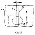
На фиг. 1 и 2 показана основная структура латеральной диффузионной разрушаемой перемычки согласно примеру выполнения изобретения с низко n легированной, узкой плоской диффузионной полосой с шириной m около 0,5 - 1 мкм, которая окружена большой p легированной областью 2. Область 2 может представлять подложку пластины с основным материалом кремнием, который уже легирован основной примесью, например бором в концентрации около 3 • 1015 см-3. Диффузионную полосу изготавливают посредством имплантации мышьяка с энергией 120 КэВ и дозой около 5,0 • 1014 см-2. Для этого самим по себе известным образом главную поверхность 31 подложки покрывают фотолаком толщиной около 1,5 мкм, экспонируют с помощью подходящей маски и проявляют. После имплантации лак удаляют, например, в содержащем кислород плазменном окружении. После имплантации диффузионной полосы следует стадия восстановления при температуре около 900oC длительностью 20 минут. Затем на главную поверхность 31 можно нанести прозрачный или, по меньшей мере, пропускающий излучение определенной длины волны покрывной слой 4. Для активирования разъемного соединительного мостика, соответственно разрушаемой перемычки 5, локально нагревают выделенный пунктирными линиями участок 6 активирования, например посредством кратковременного облучения лазерным светом подходящей длины волны, так что в области участка 6 активирования происходит обоюдная диффузия n примесей из диффузионной полосы и p примесей из p легированной области 2. При достаточно высокой концентрации p легирования области 2 область участка 6 активирования становится высокоомной, соответственно нелегированной, что приводит к размыканию n легированной диффузионной полосы.In FIG. 1 and 2 show the basic structure of the lateral diffusion destructible bridge according to an example embodiment of the invention with a low n doped narrow narrow diffusion strip with a width m of about 0.5 - 1 μm, which is surrounded by a large p doped
На фиг. 3 и 4 показана разрушаемая перемычка согласно другому примеру выполнения изобретения. При этом позициями 1 и 3-6 обозначены те же составные части, что и в примере выполнения по фиг. 1 и 2. Дополнительно диффузионной полосе придаются по обеим сторонам выполненные в подложке, состоящей из полупроводникового материала, например кремния, p+ легированные диффузионные области 7, 8, которые образованы, например, с помощью имплантации бора с энергией 20 КэВ и дозой около 5,0 • 1015 см-2 и которые имеют по сравнению с шириной m диффузионной полосы большие размеры s, t. Обе диффузионные области 7 и 8 расположены на расстоянии r друг от друга. Можно выбрать следующие размеры: m = 0,6 мкм, r = 1 мкм, s = 8 мкм, t = 10 мкм. Диффузионные области 7 и 8 выполнены в p ванне 9 в кремниевой подложке, которая может быть образована после структурирования с помощью обычных стадий фотолитографического процесса с помощью маски 10 и последующей имплантации бора с энергией около 230 КэВ и дозой 1,0 • 1013 см-2.In FIG. 3 and 4 show a breakable jumper according to another embodiment of the invention. In this case, the
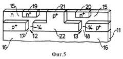
На фиг. 5 показан другой пример выполнения разрушаемой перемычки 5 согласно изобретению с двумя расположенными рядом внутри подложки, соответственно внутри ванны 11, и выполненными по отношению к главной поверхности 31 вертикально соединительными мостиками 12 и 13 с n легированными диффузионными полосами 14. Для этого две n легированные области 15 и 16 соединены друг с другом с помощью тонких, проходящих вертикально n легированных каналов 17 и 18. Для контактирования главной поверхности 31 предусмотрены две n+ легированные и таким образом низкоомные контактные области 19 и 20, которые изготавливают с помощью подходящей стадии фотолитографического процесса и подходящей стадии имплантации. Другая выполненная в главной поверхности 31 p+ легированная контактная область 21 позволяет контактирование расположенной полностью внутри подложки, соответственно n ванны 11, p+ легированной диффузионной области 22. Для активирования вертикально расположенных соединительных мостиков 12 и 13 пригодны способы нагревания, описанные уже применительно к латеральной диффузионной разрушаемой перемычке.In FIG. 5 shows another exemplary embodiment of the
На фиг. 6 и 7 показаны в схематичном виде латеральная диффузионная восстанавливаемая перемычка согласно другому примеру выполнения изобретения. Предпочтительно, высоко p+ легированная, широкая, глубокая диффузионная полоса 23 с двумя отрезками 24 и 25 токопровода с шириной около 10 мкм и длиной около 15 мкм каждый, которые выполнены на расстоянии друг от друга и образуют разрыв 26 шириной около 1 - 1,2 мкм, окружена большой низко n легированной областью 27, которая выполнена в виде n ванны 28 внутри состоящей из полупроводникового материала подложки. Подложка имеет в качестве основного материала кремний с основным легированием типа p бором, составляющим, например, 3 • 1015 см-3.In FIG. 6 and 7 are a schematic representation of a lateral diffusion reconstructed bridge according to another embodiment of the invention. Preferably, a high p+ doped, wide,
Выполненная в ней n ванна 28 может быть образована с помощью обычных стадий фотолитографического процесса и последующей имплантации фосфора с энергией около 460 КэВ и дозой 6,0 • 1012 см-2, при этом по выбору может быть затем проведена противопробойная имплантация мышьяка с энергией 320 КэВ и дозой около 8,0 • 1012 см-2. Выполненные внутри n ванны 28 отрезки 24 и 25 токопровода изготавливают после структурирования с помощью обычной стадии фотолитографического процесса, в которой наносят фотолак толщиной около 1,5 мкм, экспонируют с помощью подходящей маски и проявляют, посредством последующей имплантации бора с энергией около 20 КэВ и дозой около 5,0 • 1015 см-2. После удаления маски из фотолака посредством снятия в содержащем кислород плазменном окружении отрезки 24 и 25 токопровода восстанавливают при температуре около 900oC в течение 20 минут. Размеры и концентрации примесей отрезков 24, 25 токопровода, разрыва 26 и окружающей диффузионной области 27 выбирают так, что при достаточно высокой температуре активирования, которая превышает нормальную рабочую температуру разрыва проводника, соответственно остальных, выполненных на подложке интегральных схем, по всему расстоянию разрыва 26 отрезков 24 и 25 токопровода происходит термодинамически необратимая диффузия примесей отрезков 24, 25, 32, 33 токопровода. Посредством местного нагрева участка 30 активирования до заданной температуры активирования, например с помощью направленного на участок 30 активирования лазерного луча, происходит обоюдная взаимная диффузия n и p примесей. При достаточно высокой концентрации p+ легирования происходит p легирование участка 30 активирования и тем самым разрыва 26, что приводит к устойчивому электрическому соединению p+ легированных отрезков 24 и 25 токопровода. Также как и для разрушаемой перемычки этот процесс является необратимым; восстанавливаемая перемычка также трудно поддается контактированию. В противоположность к разрушаемой перемычке согласно фиг. 1 - 5 прямой нагрев с помощью электрического тока невозможен, однако можно использовать способы опосредованного нагревания, например резистивный нагрев с помощью размещенного поблизости проводникового меандра из поликремния (на фигурах не изображен).The
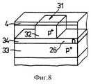
На фиг. 8 показан другой пример выполнения изобретения с вертикально расположенной диффузионной восстанавливаемой перемычкой 31 с двумя высоко p+ легированными слоями 32 и 33, которые изолированы друг от друга тонким n легированным слоем 34. Образующие оба отрезка токопровода восстанавливаемой перемычки 31 p+ легированные слои 32 и 33 с расположенным между ними, представляющим разрыв между отрезками токопровода n легированным слоем 34 могут быть изготовлены с помощью стадий имплантации или стадий эпитаксии.In FIG. Figure 8 shows another embodiment of the invention with a vertically arranged diffusion reconstructed
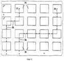
На фиг. 9 показано в качестве примера для многостороннего применения разрушаемых перемычек, соответственно восстанавливаемых перемычек, соединительное поле с множеством интегрально выполненных схемных групп 35, которые выполнены с возможность соединения посредством изображенных лишь схематично двойными стрелками диффузионных восстанавливаемых перемычек 36. В качестве примера показаны два возможных пути 37 и 38 соединения. In FIG. 9 shows, as an example, for the multilateral use of destructible jumpers, respectively, restored jumpers, a connecting field with a plurality of integrally executed
На фиг. 10А и 10В показан другой предпочтительный пример использования в виде программируемого вентиля 39 НЕ-И и программируемого вентиля 40 НЕ-ИЛИ со схематично изображенными пунктирными линиями диффузионными восстанавливаемыми перемычками а, b, с, d, e и f. Этот пример выполнения особенно пригоден для последующих модификаций испытываемых схем, в которых с помощью активирования восстанавливаемых перемычек а, b, с, соответственно d, e, f, и соответствующего переключения МОП транзисторов T, соответственно подключения к питающему напряжению Vdd и массе Vss, можно реализовать функцию НЕ-И или НЕ-ИЛИ с входами E1, E2 и выходом Aus.In FIG. 10A and 10B show another preferred example of use as a
На фиг. 11А показан схематично вид сверху размещения таких программируемых вентилей 39 и 40 НЕ-И и НЕ-ИЛИ, при этом на фиг. 11В приведено пояснение символов отдельных слоев. In FIG. 11A is a schematic plan view of the arrangement of such programmable NON-AND and NOR
Claims (21)
Translated fromRussian- заготовка подложки, состоящей из полупроводникового материала первого типа проводимости;
- выполнение электрически проводящего, в продольном направлении непрерывного, поперек продольного направления имеющего заданную ширину токопровода второго типа проводимости, противоположного первому типу проводимости, в состоящей их полупроводникового материала подложке;
- нагревание участка (30) активирования, охватывающего токопровод и, по меньшей мере, часть полупроводникового материала подложки, до заданной температуры активирования, которая превышает рабочую температуру соединительного мостика (1, 12, 13), для необратимого разъединения по всей ширине токопровода посредством диффузии полупроводникового материала первого типа проводимости и/или материала токопровода.16. A method of manufacturing and activating a separable connecting bridge (destructible jumper), comprising the following stages:
- the preparation of the substrate, consisting of a semiconductor material of the first type of conductivity;
- the implementation of an electrically conductive, in the longitudinal direction, continuous, transverse to the longitudinal direction, having a given width of the conductors of the second type of conductivity, opposite to the first type of conductivity, in the substrate consisting of a semiconductor material;
- heating the activation section (30), covering the current lead and at least a portion of the semiconductor substrate material, to a predetermined activation temperature, which exceeds the operating temperature of the connecting bridge (1, 12, 13), for irreversible separation across the entire width of the current lead through diffusion of the semiconductor material of the first type of conductivity and / or conductor material.
- выполнение электрически проводящего токопровода (23) посредством легирования примесью образующих в продольном направлении разрыв заданного размера отрезков (24, 25, 32, 33) токопровода первого типа проводимости в подложке, состоящей из полупроводникового материала второго типа проводимости, противоположного первому типу проводимости, и
- нагревание участка (30) активирования, охватывающего разрыв (26) отрезков (24, 25, 32, 33) токопровода, до заданной температуры активирования, которая превышает рабочую температуру разрыва проводника, для необратимой диффузии примеси отрезков (24, 25, 32, 33) токопровода по всему разрыву (26) токопровода (23).18. A method of manufacturing and activating a connected gap of the conductor (restored jumper), containing the following stages:
- the implementation of an electrically conductive current lead (23) by doping with an impurity forming in the longitudinal direction a gap of a predetermined size of the segments (24, 25, 32, 33) of the first type conductivity conductor in a substrate consisting of a semiconductor material of a second type of conductivity opposite to the first type of conductivity, and
- heating of the activation section (30), covering the gap (26) of the segments (24, 25, 32, 33) of the current lead, to a predetermined activation temperature, which exceeds the working temperature of the conductor rupture, for irreversible diffusion of the impurity of the segments (24, 25, 32, 33 ) conductors along the entire gap (26) of the conductors (23).
Priority Applications (1)
| Application Number | Priority Date | Filing Date | Title |
|---|---|---|---|
| RU98116790ARU2172539C2 (en) | 1996-02-09 | 1997-02-06 | Separable junction bridge (destructible jumper) and connectable open circuit (re-connectable jumper); method for manufacturing and activating destructible and re-connectable jumpers |
Applications Claiming Priority (2)
| Application Number | Priority Date | Filing Date | Title |
|---|---|---|---|
| DE19604776.5 | 1996-02-09 | ||
| RU98116790ARU2172539C2 (en) | 1996-02-09 | 1997-02-06 | Separable junction bridge (destructible jumper) and connectable open circuit (re-connectable jumper); method for manufacturing and activating destructible and re-connectable jumpers |
Publications (2)
| Publication Number | Publication Date |
|---|---|
| RU98116790A RU98116790A (en) | 2000-06-27 |
| RU2172539C2true RU2172539C2 (en) | 2001-08-20 |
Family
ID=48235512
Family Applications (1)
| Application Number | Title | Priority Date | Filing Date |
|---|---|---|---|
| RU98116790ARU2172539C2 (en) | 1996-02-09 | 1997-02-06 | Separable junction bridge (destructible jumper) and connectable open circuit (re-connectable jumper); method for manufacturing and activating destructible and re-connectable jumpers |
Country Status (1)
| Country | Link |
|---|---|
| RU (1) | RU2172539C2 (en) |
Citations (8)
| Publication number | Priority date | Publication date | Assignee | Title |
|---|---|---|---|---|
| US4050083A (en)* | 1976-09-22 | 1977-09-20 | Cutler-Hammer, Inc. | Integrated thermally sensitive power switching semiconductor device, including a thermally self-protected version |
| US4278985A (en)* | 1980-04-14 | 1981-07-14 | Gte Laboratories Incorporated | Monolithic integrated circuit structure incorporating Schottky contact diode bridge rectifier |
| US4281448A (en)* | 1980-04-14 | 1981-08-04 | Gte Laboratories Incorporated | Method of fabricating a diode bridge rectifier in monolithic integrated circuit structure utilizing isolation diffusions and metal semiconductor rectifying barrier diode formation |
| US4903111A (en)* | 1983-12-06 | 1990-02-20 | Fujitsu Limited | Integrated circuit device |
| US5202275A (en)* | 1989-03-20 | 1993-04-13 | Hitachi Ltd. | Semiconductor integrated circuit device, process for fabricating the same, and apparatus for fabricating the same |
| RU2024110C1 (en)* | 1991-04-10 | 1994-11-30 | Научно-исследовательский институт точной технологии | Integrated circuit |
| US5426613A (en)* | 1989-03-20 | 1995-06-20 | Hitachi, Ltd. | Semiconductor memory device with improved substrate arrangement to permit forming a plurality of different types of random access memory, and a testing method therefor |
| US5436496A (en)* | 1986-08-29 | 1995-07-25 | National Semiconductor Corporation | Vertical fuse device |
- 1997
- 1997-02-06RURU98116790Apatent/RU2172539C2/ennot_activeIP Right Cessation
Patent Citations (9)
| Publication number | Priority date | Publication date | Assignee | Title |
|---|---|---|---|---|
| US4050083A (en)* | 1976-09-22 | 1977-09-20 | Cutler-Hammer, Inc. | Integrated thermally sensitive power switching semiconductor device, including a thermally self-protected version |
| US4278985A (en)* | 1980-04-14 | 1981-07-14 | Gte Laboratories Incorporated | Monolithic integrated circuit structure incorporating Schottky contact diode bridge rectifier |
| US4281448A (en)* | 1980-04-14 | 1981-08-04 | Gte Laboratories Incorporated | Method of fabricating a diode bridge rectifier in monolithic integrated circuit structure utilizing isolation diffusions and metal semiconductor rectifying barrier diode formation |
| US4903111A (en)* | 1983-12-06 | 1990-02-20 | Fujitsu Limited | Integrated circuit device |
| US5436496A (en)* | 1986-08-29 | 1995-07-25 | National Semiconductor Corporation | Vertical fuse device |
| US5202275A (en)* | 1989-03-20 | 1993-04-13 | Hitachi Ltd. | Semiconductor integrated circuit device, process for fabricating the same, and apparatus for fabricating the same |
| US5331191A (en)* | 1989-03-20 | 1994-07-19 | Hitachi, Ltd. | Semiconductor integrated circuit device, process for fabricating the same, and apparatus for fabricating the same |
| US5426613A (en)* | 1989-03-20 | 1995-06-20 | Hitachi, Ltd. | Semiconductor memory device with improved substrate arrangement to permit forming a plurality of different types of random access memory, and a testing method therefor |
| RU2024110C1 (en)* | 1991-04-10 | 1994-11-30 | Научно-исследовательский институт точной технологии | Integrated circuit |
Similar Documents
| Publication | Publication Date | Title |
|---|---|---|
| KR0157348B1 (en) | Programmable fuse structure and fuse programming method | |
| US3792319A (en) | Poly-crystalline silicon fusible links for programmable read-only memories | |
| JP2721529B2 (en) | Electrically programmable low impedance non-fuse element | |
| US5827759A (en) | Method of manufacturing a fuse structure | |
| US5852323A (en) | Electrically programmable antifuse using metal penetration of a P-N junction | |
| KR930011702B1 (en) | High power semiconductor device | |
| CN100539115C (en) | Semiconductor device | |
| CN1547773A (en) | Optical and Electrically Programmable Siliconized Polysilicon Fuse Devices | |
| KR100414239B1 (en) | Separable connecting bridge (fuse) and connectable line interruption (anti-fuse) and process for producing and activating a fuse and an anti-fuse | |
| RU2172539C2 (en) | Separable junction bridge (destructible jumper) and connectable open circuit (re-connectable jumper); method for manufacturing and activating destructible and re-connectable jumpers | |
| JP4034992B2 (en) | Semiconductor device | |
| JPH0541481A (en) | Semiconductor integrated circuit | |
| US20050133882A1 (en) | Integrated circuit fuse and method of fabrication | |
| JPH0760853B2 (en) | Laser beam programmable semiconductor device and manufacturing method of semiconductor device | |
| US6388289B1 (en) | Semiconductor device having electrostatic discharge protection circuit | |
| JPS6059678B2 (en) | Programmable read-only memory device | |
| JPS62172739A (en) | Semiconductor integrated circuit | |
| KR20070015910A (en) | Integrated Circuit Fuses and Manufacturing Methods | |
| JPS63291433A (en) | Fuse element | |
| JPS6181654A (en) | Laser beam programmable semiconductor device and making thereof | |
| JPH03250734A (en) | Manufacturing method of semiconductor integrated circuit | |
| JPH0383360A (en) | Semiconductor device | |
| JPH0365903B2 (en) | ||
| JPH0548627B2 (en) | ||
| HK1003959A (en) | Fuse structure for an integrated circuit device |
Legal Events
| Date | Code | Title | Description |
|---|---|---|---|
| MM4A | The patent is invalid due to non-payment of fees | Effective date:20070207 |