RU2166834C2 - Switching power amplifier using analog correction of output voltage - Google Patents
Switching power amplifier using analog correction of output voltageDownload PDFInfo
- Publication number
- RU2166834C2 RU2166834C2RU99111489ARU99111489ARU2166834C2RU 2166834 C2RU2166834 C2RU 2166834C2RU 99111489 ARU99111489 ARU 99111489ARU 99111489 ARU99111489 ARU 99111489ARU 2166834 C2RU2166834 C2RU 2166834C2
- Authority
- RU
- Russia
- Prior art keywords
- output
- input
- voltage
- controlled rectifier
- key
- Prior art date
Links
- 238000004804windingMethods0.000claimsdescription70
- 238000009499grossingMethods0.000claimsdescription13
- 230000003321amplificationEffects0.000claimsdescription6
- 238000003199nucleic acid amplification methodMethods0.000claimsdescription6
- XUKUURHRXDUEBC-KAYWLYCHSA-NAtorvastatinChemical compoundC=1C=CC=CC=1C1=C(C=2C=CC(F)=CC=2)N(CC[C@@H](O)C[C@@H](O)CC(O)=O)C(C(C)C)=C1C(=O)NC1=CC=CC=C1XUKUURHRXDUEBC-KAYWLYCHSA-N0.000claims1
- 239000000126substanceSubstances0.000abstract1
- 239000003990capacitorSubstances0.000description6
- 238000010586diagramMethods0.000description6
- 230000002452interceptive effectEffects0.000description2
- MJYQFWSXKFLTAY-OVEQLNGDSA-N(2r,3r)-2,3-bis[(4-hydroxy-3-methoxyphenyl)methyl]butane-1,4-diol;(2r,3r,4s,5s,6r)-6-(hydroxymethyl)oxane-2,3,4,5-tetrolChemical compoundOC[C@H]1O[C@@H](O)[C@H](O)[C@@H](O)[C@@H]1O.C1=C(O)C(OC)=CC(C[C@@H](CO)[C@H](CO)CC=2C=C(OC)C(O)=CC=2)=C1MJYQFWSXKFLTAY-OVEQLNGDSA-N0.000description1
- 241001050985DiscoSpecies0.000description1
- 238000005265energy consumptionMethods0.000description1
- 235000004426flaxseedNutrition0.000description1
- 239000004065semiconductorSubstances0.000description1
Images


Landscapes
- Rectifiers (AREA)
Abstract
Description
Translated fromRussianНастоящее изобретение относится к коммутационным усилителям, а более точно касается коммутационного усилителя мощности с аналоговой коррекцией выходного напряжения. The present invention relates to switching amplifiers, and more particularly relates to a switching power amplifier with analog output voltage correction.
Данное изобретение может быть использовано в устройствах усиления мощности для проведения дискотек, для озвучивания концертных, спортивных, кинозалов, для радиотрансляционной сети общего назначения. This invention can be used in power amplification devices for holding discos, for sounding concert, sports, cinema halls, for a general purpose broadcasting network.
Известен коммутационный усилитель (Павлов В.Н., Ногин В.Н. Схемотехника аналоговых электронных устройств: Учебник для вузов. - М.: Радио и связь. 1997, стр. 162, рис. 9.5), содержащий источник питания, состоящий из двух отдельных источников, клемму для подключения входного сигнала, элементы усиления, резистор для ограничения насыщения элемента усиления. Элементы усиления выполнены в виде биполярных транзисторов. Эмиттер первого транзистора соединен с нагрузкой, его база соединена через резистор для ограничения насыщения с клеммой для подключения входного сигнала, а коллектор соединен с катодом отключающего диода. Эмиттер второго транзистора соединен с коллектором первого транзистора, база его соединена с клеммой для подключения входного сигнала, а коллектор соединен со вторым источником питания. Причем анод отключающего диода соединен с первым источником питания. Known switching amplifier (Pavlov VN, Nogin VN Circuitry of analog electronic devices: Textbook for high schools. - M .: Radio and communications. 1997, p. 162, Fig. 9.5), containing a power source consisting of two separate sources, a terminal for connecting the input signal, gain elements, a resistor to limit the saturation of the gain element. The gain elements are made in the form of bipolar transistors. The emitter of the first transistor is connected to the load, its base is connected through a resistor to limit saturation with a terminal for connecting the input signal, and the collector is connected to the cathode of the trip diode. The emitter of the second transistor is connected to the collector of the first transistor, its base is connected to the terminal for connecting the input signal, and the collector is connected to the second power source. Moreover, the anode of the disconnecting diode is connected to the first power source.
Работа усилителя происходит следующим образом. При входном напряжении меньшем, чем напряжение от первого источника питания, второй выключен, а первый транзистор работает как усилительный элемент, причем питание на него подается через отключающий диод с первого источника питания. При повышении входного напряжения выше, чем питающее напряжение от первого источника питания начинает открываться второй транзистор, отключающий диод закрывается, а первый транзистор полностью открывается. Таким образом, роль элемента усиления берет на себя второй транзистор, а напряжение питания теперь равно напряжению от второго источника питания. В данном усилителе мощности для создания нескольких ступеней питающего напряжения с целью дальнейшего повышения коэффициента полезного действия устройства необходимо добавить столько же отдельных источников питания и столько же элементов усиления, сколько ступеней питающего напряжения. Причем на каждом элементе усиления в открытом его состоянии рассеивается дополнительная мощность. Таким образом уменьшается общий коэффициент полезного действия устройства, а из-за увеличения количества питающих источников снижается надежность всего устройства. The operation of the amplifier is as follows. When the input voltage is lower than the voltage from the first power source, the second is turned off, and the first transistor acts as an amplifying element, and power is supplied to it through a disconnecting diode from the first power source. When the input voltage is higher than the supply voltage from the first power source, the second transistor starts to open, the disconnecting diode closes, and the first transistor opens completely. Thus, the role of the gain element is taken over by the second transistor, and the supply voltage is now equal to the voltage from the second power source. In this power amplifier, to create several stages of supply voltage in order to further increase the efficiency of the device, it is necessary to add as many separate power sources and as many gain elements as stages of supply voltage. Moreover, additional power is dissipated on each gain element in its open state. Thus, the overall efficiency of the device is reduced, and due to the increase in the number of supply sources, the reliability of the entire device is reduced.
В основу изобретения положена задача создания коммутационного усилителя мощности с аналоговой коррекцией выходного напряжения, позволяющего за счет нового схематического решения достичь уменьшения потерь мощности на элементах усиления при заданном количестве ступеней питающего напряжения, уменьшить количество источников питания, что в свою очередь позволяет повысить коэффициент полезного действия и надежность всего усилителя. The basis of the invention is the task of creating a switching power amplifier with analog correction of the output voltage, which allows, due to a new schematic solution, to reduce power losses on the amplification elements for a given number of supply voltage steps, to reduce the number of power sources, which in turn allows to increase the efficiency and reliability of the entire amplifier.
Поставленная задача решается тем, что в коммутационном усилителе мощности с аналоговой коррекцией выходного напряжения, содержащем источник напряжения питания, элемент усиления, клемму для подключения входного сигнала, согласно изобретению источник напряжения питания имеет два источника переменного опорного напряжения, подключенных к n разрядным ячейкам с n ключевыми элементами, управляемый выпрямитель, подключенный к последовательно соединенным выходам n разрядных ячеек и соединенный своими выходами с фильтром, первый выход которого подключен к нагрузке, аналого-цифровой преобразователь, предназначенный для управления n разрядными ячейками, первый выход которого подключен к управляющему входу управляемого выпрямителя, а остальные n выходов подключены к соответствующим n ключевым элементам, а вход его подключен к клемме для подключения входного сигнала, синхронизирующий вход управляемого выпрямителя соединен со вторым источником переменного напряжения, элемент усиления выполнен в виде аналогового усилителя мощности, выход которого соединен со вторым выходом фильтра, также коммутационный усилитель мощности содержит делитель напряжения, выполненный на двух последовательно соединенных резисторах, начало первого резистора подключено к нагрузке, выход делителя напряжения соединен с инвертирующим входом аналогового усилителя мощности, конец второго резистора соединен с шиной заземления, неинвертирующий вход аналогового усилителя мощности подключен к клемме для подключения входного сигнала, каждая из n разрядных ячеек содержит делитель опорного напряжения, выполненный в виде трансформатора напряжения с последовательно соединенными первой и второй первичными обмотками и вторичной обмоткой, при этом начало вторичной обмотки трансформатора первой разрядной ячейки соединено с первым входом управляемого выпрямителя, конец вторичной обмотки трансформатора n-ной разрядной ячейки соединен со вторым входом отправляемого выпрямителя, вторичные обмотки трансформаторов всех n разрядных ячеек соединены последовательно, каждая разрядная ячейка содержит первый диод, анод которого соединен с первым источником переменного опорного напряжения, катод которого соединен с началом первой первичной обмотки соответствующего трансформатора, второй диод, анод которого соединен со вторым источником переменного опорного напряжения, а катод его соединен с концом второй первичной обмотки соответствующего трансформатора, шунтирующий диод, анод которого соединен с общей точкой последовательно соединенных первой и второй первичных обмоток соответствующего трансформатора и через соответствующий ключевой элемент с шиной заземления, катод которого соединен с шиной питания. The problem is solved in that in a switching power amplifier with analog output voltage correction, comprising a power supply source, a gain element, a terminal for connecting an input signal, according to the invention, the power supply source has two AC voltage sources connected to n discharge cells with n key elements, a controlled rectifier connected to the series-connected outputs of n bit cells and connected to the outputs with a filter, the first output of which o connected to the load, an analog-to-digital converter designed to control n discharge cells, the first output of which is connected to the control input of a controlled rectifier, and the remaining n outputs are connected to the corresponding n key elements, and its input is connected to the terminal for connecting the input signal, synchronizing the input of the controlled rectifier is connected to the second source of alternating voltage, the amplification element is made in the form of an analog power amplifier, the output of which is connected to the second output ph liter, also the switching power amplifier contains a voltage divider made on two series-connected resistors, the beginning of the first resistor is connected to the load, the output of the voltage divider is connected to the inverting input of the analog power amplifier, the end of the second resistor is connected to the ground bus, the non-inverting input of the analog power amplifier is connected to terminal for connecting the input signal, each of the n bit cells contains a voltage divider made in the form of a transformer n voltages with the first and second primary windings and the secondary winding connected in series, with the beginning of the secondary winding of the transformer of the first bit cell connected to the first input of the controlled rectifier, the end of the secondary winding of the transformer of the n-th bit cell connected to the second input of the sent rectifier, the secondary windings of transformers of all n bit cells are connected in series, each bit cell contains a first diode, the anode of which is connected to the first source of variable reference voltage, the cathode of which is connected to the beginning of the first primary winding of the corresponding transformer, the second diode, the anode of which is connected to the second source of alternating voltage reference, and its cathode is connected to the end of the second primary winding of the corresponding transformer, a shunt diode, the anode of which is connected to the common point of the first connected in series and the second primary windings of the corresponding transformer and through the corresponding key element with a ground bus, the cathode of which is connected to the power bus.
Возможно, что управляемый выпрямитель содержит первый, второй, третий, четвертый ключи переменного тока и первый, второй, третий, четвертый блоки управления, при этом первый и второй входы первого ключа переменного тока соединены соответственно с первым и вторым выходами первого блока управления, а его первый и второй выходы являются соответственно первым входом и вторым выходами управляемого выпрямителя, первый и второй входы второго ключа переменного тока соединены соответственно с первым и вторым выходами второго блока управления, а его первый выход соединен со вторым выходом первого ключа переменного тока, второй его выход является вторым входом управляемого выпрямителя, первый и второй входы третьего ключа переменного тока соединены соответственно с первым и вторым выходами третьего блока управления, его первый выход является первым выходом управляемого выпрямителя, а его второй выход соединен со вторым выходом второго ключа переменного тока, первый и второй входы четвертого ключа переменного тока соединены соответственно с первым и вторым выходами четвертого блока управления, его первый выход соединен с первым выходом первого ключа переменного тока, а его второй выход соединен с первым выходом третьего ключа переменного тока, первые входы первого и третьего блоков управления подключены к выходу операционного усилителя, вторые их входы подключены к шине заземления, первые входы второго и четвертого блоков управления подключены к шине заземления, а их вторые входы соединены с выходом операционного усилителя, инвертирующий вход которого подключен к источнику напряжения смещения, а его неинвертирующий вход подключен к выходу логического элемента ИСКЛЮЧАЮЩЕЕ ИЛИ, первый и второй входы логического элемента ИСКЛЮЧАЮЩЕЕ ИЛИ являются соответственно синхронизирующим и управляющим входами управляемого выпрямителя. It is possible that the controlled rectifier contains the first, second, third, fourth alternating current keys and the first, second, third, fourth control units, while the first and second inputs of the first alternating current key are connected respectively to the first and second outputs of the first control unit, and its the first and second outputs are respectively the first input and second outputs of the controlled rectifier, the first and second inputs of the second AC key are connected respectively to the first and second outputs of the second control unit, and its first output is connected to the second output of the first AC key, its second output is the second input of the controlled rectifier, the first and second inputs of the third AC key are connected respectively to the first and second outputs of the third control unit, its first output is the first output of the controlled rectifier, and its second output is connected to the second output of the second alternating current key, the first and second inputs of the fourth alternating current key are connected respectively to the first and second outputs of the fourth of the control unit, its first output is connected to the first output of the first alternating current key, and its second output is connected to the first output of the third alternating current key, the first inputs of the first and third control units are connected to the output of the operational amplifier, their second inputs are connected to the ground bus, the first the inputs of the second and fourth control units are connected to the ground bus, and their second inputs are connected to the output of the operational amplifier, the inverting input of which is connected to a bias voltage source, and its non-inverter The timing input is connected to the output of the EXCLUSIVE OR logic element, the first and second inputs of the EXCLUSIVE OR logic element are respectively the synchronizing and control inputs of the controlled rectifier.
Целесообразно, чтобы трансформатор напряжения делителя опорного напряжения каждой из n разрядных ячеек содержал дополнительную вторичную обмотку, дополнительные вторичные обмотки всех трансформаторов соединены между собой последовательно, начало дополнительной вторичной обмотки трансформатора n-ной разрядной ячейки соединено с концом вторичной обмотки трансформатора n-ной разрядной ячейки, управляемый выпрямитель дополнительно имеет третий вход, соединенный с концом дополнительной вторичной обмотки трансформатора первой разрядной ячейки. It is advisable that the voltage transformer of the reference voltage divider of each of the n bit cells contains an additional secondary winding, the additional secondary windings of all the transformers are connected together in series, the beginning of the additional secondary winding of the transformer of the n-th bit cell is connected to the end of the secondary winding of the transformer of the n-bit bit cell, the controlled rectifier additionally has a third input connected to the end of the additional secondary winding of the transformer of the first discharge oh cell.
Также целесообразно, чтобы управляемый выпрямитель содержал первый и второй ключи переменного тока, первый и второй блоки управления, первый и второй входы первого ключа переменного тока соединены соответственно с первым и вторым выходами первого блока управления, а первый выход первого ключа переменного тока является первым входом управляемого выпрямителя, первый и второй входы второго ключа переменного тока соединены соответственно с первым и вторым выходами второго блока управления, второй вход управляемого выпрямителя соединен с первым его выходом, а первый выход второго ключа переменного тока является третьим входом управляемого выпрямителя, второй его выход соединен со вторым выходом первого ключа переменного тока, который является вторым выходом управляемого выпрямителя, первый вход первого блока управления соединен с выходом операционного усилителя, а его второй вход соединен с шиной заземления, первый вход второго блока управления соединен с шиной заземления, а его второй вход соединен с выходом операционного усилителя, инвертирующий вход которого подключен к источнику напряжения смещения, а его неинвертирующий вход подключен к выходу логического элемента ИСКЛЮЧАЮЩЕЕ ИЛИ, первый и второй входы логического элемента ИСКЛЮЧАЮЩЕЕ ИЛИ являются соответственно синхронизирующим и управляющим входами управляемого выпрямителя. It is also advisable that the controlled rectifier contains the first and second AC keys, the first and second control units, the first and second inputs of the first AC key are connected respectively to the first and second outputs of the first control unit, and the first output of the first AC key is the first input of the controlled rectifier, the first and second inputs of the second AC key are connected respectively to the first and second outputs of the second control unit, the second input of the controlled rectifier is connected to its first output, and the first output of the second AC key is the third input of the controlled rectifier, its second output is connected to the second output of the first AC key, which is the second output of the controlled rectifier, the first input of the first control unit is connected to the output of the operational amplifier, and its second the input is connected to the ground bus, the first input of the second control unit is connected to the ground bus, and its second input is connected to the output of the operational amplifier, the inverting input of which is connected is biased to the bias voltage source, and its non-inverting input is connected to the output of the EXCLUSIVE OR logic element, the first and second inputs of the EXCLUSIVE OR logic element are respectively the synchronizing and control inputs of the controlled rectifier.
Данный коммутационный усилитель мощности с аналоговой коррекцией выходного напряжения обладает повышенным коэффициентом полезного действия и повышенной надежностью. Данное изобретение позволяет уменьшить потери мощности на усилительном элементе и создать 2n питающих напряжения при использовании всего n источников питания. Также, данное изобретение позволяет получить большую выходную мощность устройства при меньшем потреблении энергии из питающей сети за счет высокого коэффициента полезного действия. Данное изобретение увеличивает динамический диапазон выходного напряжения всего устройства при меньшем количестве источников питания. Также данное изобретение отличается простотой реализации, использует стандартные, широко используемые в промышленности элементы, широко взаимозаменяемые по типажу в зависимости от требуемой выходной мощности и других его характеристик.This switching power amplifier with analog output voltage correction has a high efficiency and increased reliability. This invention allows to reduce the power loss on the amplifying element and to create 2n supply voltage using only n power sources. Also, this invention allows to obtain a large output power of the device with less energy consumption from the supply network due to the high efficiency. This invention increases the dynamic range of the output voltage of the entire device with fewer power sources. Also, this invention is simple to implement, uses standard elements widely used in industry that are widely interchangeable in type depending on the required output power and its other characteristics.
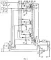
В дальнейшем изобретение поясняется конкретными примерами выполнения и чертежами, на которых
фиг. 1 изображает принципиальную схему коммутационного усилителя мощности с аналоговой коррекцией выходного напряжения согласно изобретению;
фиг. 2 изображает принципиальную схему управляемого выпрямителя согласно изобретению;
фиг. 3 изображает принципиальную схему второго варианта усилителя мощности с наличием у трансформаторов дополнительной вторичной обмотки согласно изобретению;
фиг. 4 изображает принципиальную схему управляемого выпрямителя, применяемого при втором варианте усилителя мощности согласно изобретению.The invention is further illustrated by specific examples and drawings, in which
FIG. 1 is a circuit diagram of a switching power amplifier with analog output voltage correction according to the invention;
FIG. 2 is a circuit diagram of a controlled rectifier according to the invention;
FIG. 3 shows a schematic diagram of a second embodiment of a power amplifier with transformers having an additional secondary winding according to the invention;
FIG. 4 is a circuit diagram of a controlled rectifier used in a second embodiment of a power amplifier according to the invention.
фиг. 5 изображает принципиальную схему сглаживающего фильтра согласно изобретению. FIG. 5 is a circuit diagram of a smoothing filter according to the invention.
Коммутационный усилитель мощности с аналоговой коррекцией выходного напряжения содержит источник 1 (фиг. 1) напряжения питания, элементы 2 усиления, клемму 3 для подключения входного сигнала. Источник 1 напряжения питания имеет два источника 4, 5 переменного напряжения, подключенные к n разрядным ячейкам 61,...6n с n ключевыми элементами 71,...7n, управляемый выпрямитель 8, подключенный к последовательно соединенным выходам n разрядных ячеек 61,...6n и соединенный своими выходами с сглаживающим фильтром 9, первый выход 10 которого подключен к нагрузке 11. Усилитель содержит аналого-цифровой преобразователь 12, предназначенный для управления n разрядными ячейками 61, ...6n, первый выход 13 которого подключен к управляющему входу 14 управляемого выпрямителя 8, а остальные n выходов 151,...15n подключены к соответствующим n ключевым элементам 71,...7n, а вход его подключен к клемме 3 для подключения входного сигнала. Элемент 2 усиления выполнен в виде общеизвестного аналогового усилителя мощности (Прянишников В.Д., "Электроника: курс лекций" Спб: Корона принт, 1998 г., стр. 146, рис. 8.9). Коммутационный усилитель содержит также делитель напряжения, выполненный на двух последовательно соединенных резисторах 16, 17. Начало первого резистора подключено к нагрузке 11. Выход делителя напряжения соединен с инвертирующим входом 18 аналогового усилителя мощности. Конец второго резистора соединен с шиной 19 заземления. Неинвертирующий вход 20 подключен к клемме 3 для подключения входного сигнала, а его выход соединен со вторым выходом 21 фильтра 9. Каждая из n разрядных ячеек 61,...6n содержит делитель опорного напряжения, выполненный в виде трансформатора 22 напряжения с последовательно соединенными первой и второй первичными обмотками 23, 24 и вторичной обмоткой 25, при этом вторичные обмотки 25 трансформаторов 22 всех n разрядных ячеек 61,...6n соединены последовательно, каждая из n разрядных ячеек 61,...6n содержит первый диод 26, анод которого соединен с первым источником 4 переменного опорного напряжения, катод которого соединен с началом первой первичной обмотки 23 соответствующего трансформатора 22, второй диод 27, анод которого соединен со вторым источником 5 переменного опорного напряжения, а катод его соединен с концом второй первичной обмотки 24 соответствующего трансформатора 22, шунтирующий диод 28, анод которого соединен с общей точкой 29 последовательно соединенных первой и второй первичных обмоток 23, 24 соответствующего трансформатора 22 и через соответствующий ключевой элемент 71,...7n с шиной 19 заземления, катод которого соединен с шиной 30 питания. Начало вторичной обмотки 25 первой разрядной ячейки 61 соединено с первым входом 31 управляемого выпрямителя 8. Конец вторичной обмотки 25 трансформатора ячейки 6n соединен со вторым входом 32 управляемого выпрямителя 8, синхронизирующий вход 33 которого соединен со вторым источником 5 переменного напряжения. Источники 4, 5 переменного опорного напряжения, фильтр 9, аналого-цифровой преобразователь 12 выполнены по общеизвестным схемам, см. Прянишников В.Д. "Электроника. Курс лекций" Спб: Корона, 1998 г., соответственно стр. 373, рис. 33.9; стр. 377, рис. 33.13; стр. 282, рис. 26.6.A switching power amplifier with analog output voltage correction comprises a power supply source 1 (Fig. 1),
Управляемый выпрямитель содержит первый, второй, третий, четвертый ключи 34, 35, 36, 37 (фиг. 2) переменного тока и первый, второй, третий, четвертый блоки 38, 39, 40, 41 управления. При этом первый и второй входы первого ключа 34 переменного тока соединены соответственно с первым и вторым выходами первого блока 38 управления, а его первый и второй выходы являются соответственно первым входом 31 и вторым выходом управляемого выпрямителя 8. Первый и второй входы второго ключа 35 переменного тока соединены соответственно с первым и вторым выходами второго блока 39 управления, а его первый выход 42 соединен со вторым выходом первого ключа 34 переменного тока. Второй его выход является вторым входом 32 управляемого выпрямителя 8. Первый и второй входы третьего ключа 36 соединены соответственно с первым и вторым выходами третьего блока 40 управления. Его первый выход является первым выходом управляемого выпрямителя 8, а его второй выход 43 соединен со вторым выходом второго ключа 35. Первый и второй входы четвертого ключа 37 соединены соответственно с первым и вторым выходами четвертого блока 41 управления. Его первый выход 44 соединен с первым выходом первого ключа 34, а его второй выход соединен с первым выходом третьего ключа 36. Первые входы первою блока 38 и третьего блока 40 управления подключены к выходу операционного усилителя 45. Вторые их входы подключены к шине 19 заземления. Первые входы второго блока 39 и четвертого блока 41 управления подключены к шине 19 заземления. Их вторые входы соединены с выходом операционного усилителя 45, инвертирующий вход 46 которого подключен к источнику 47 напряжения смещения, а его неинвертирующий вход 48 подключен к выходу логического элемента 49 ИСКЛЮЧАЮЩЕЕ ИЛИ. Первый и второй входы логического элемента 49 являются соответственно синхронизирующим входом 33 и управляющим входом 14 управляемого выпрямителя 8. На фигуре 3 показан второй вариант выполнения коммутационного усилителя мощности с аналоговой коррекцией выходного напряжения, аналогичный коммутационному усилителю мощности, изображенному на фиг. 1 Отличие заключается лишь в том, что трансформатор 22 каждой из n ячеек 61,.. . 6n содержит дополнительную вторичную обмотку 50. Все дополнительные вторичные обмотки 50 соединены последовательно между собой. Конец дополнительной вторичной обмотки 50 первой разрядной ячейки 61 соединен с дополнительным входом 51 управляемого выпрямителя 8, а начало дополнительной вторичной обмотки 50 n-ной разрядной ячейки 6n соединено с концом вторичной обмотки 25 трансформатора 22 n-ной разрядной ячейки 6n.The controlled rectifier contains the first, second, third,
На фигуре 4 изображен управляемый выпрямитель, используемый в усилителе мощности, изображенном на фигуре 3. Управляемый выпрямитель содержит первый, второй ключи 52, 53 переменного тока и первый, второй блоки 54, 55 управления. Первый и второй входы первого ключа 52 переменного тока соединены соответственно с первым и вторым выходами первого блока 54 управления, а его первый выход является первым входом 31 управляемого выпрямителя 8. Figure 4 shows a controlled rectifier used in the power amplifier shown in figure 3. The controlled rectifier contains the first, second alternating
Первый выход управляемого выпрямителя 8 является вторым входом 32 управляемого выпрямителя 8. Первый и второй входы второго ключа 53 переменного тока соединены соответственно с первым и вторым выходами второго блока 55 управления. Его первый выход является третьим входом 51 управляемого выпрямителя 8, а его второй выход соединен со вторым выходом первого ключа 52 переменного тока и является вторым выходом управляемого выпрямителя 8. Первый вход первого блока 54 управления соединен с выходом операционного усилителя 56, а его второй вход соединен с шиной 19 заземления. Первый вход второго блока 55 управления соединен с шиной 19 заземления, а его второй вход соединен с выходом операционного усилителя 56, инвертирующий вход 57, неинвертирующий вход 58 которого подключены соответственно к источнику 59 напряжения смещения и к выходу логического элемента 60 ИСКЛЮЧАЮЩЕЕ ИЛИ. Первый и второй входы логического элемента 60 ИСКЛЮЧАЮЩЕЕ ИЛИ являются соответственно синхронизирующим входом 33 и управляющим входом 14 управляемого выпрямителя 8. При этом второй вход 32 выпрямителя соединен с первым его выходом. В качестве операционного усилителя 45 (фиг. 2), 56 (фиг. 4) используются общеизвестные операционные усилители (Прянишников В.Д., "Электроника: курс лекций" Спб: Корона принт, 1998 г., стр. 86, рис. 8.4б). The first output of the controlled
На фигуре 5 изображена принципиальная схема сглаживающего фильтра 9, содержащего конденсатор 61 и индуктивность 62. Первый вывод конденсатора 61 является первым входом сглаживающего фильтра 9. Второй вывод конденсатора 61 подсоединен к первому выводу индуктивности 62. Второй вывод индуктивности 62 является вторым входом сглаживающего фильтра 9. Первый вывод конденсатора 61 является первым выходом 10 сглаживающего фильтра 9. Второй вывод конденсатора 61 является вторым выходом 21 сглаживающего фильтра 9. Figure 5 shows a schematic diagram of a smoothing
Точками на фигурах 1, 3 обозначено начало обмоток 24 (фиг. 1), 25, 50 (фиг. 3) трансформатора 22. По направлению стрелок А показано протекание токов в данной схеме. Ключи 34 (фиг. 2), 35, 36, 37, 52 (фиг. 4), 53 выполнены по стандартной схеме, а блоки 38 (фиг. 2), 39, 40, 41, 55 (фиг. 4), 54 также выполнены по стандартной общеизвестной схеме, см. "Силовые, полупроводниковые приборы" под ред. В.В.Токарева, Воронеж, 1995 г., изд-во ТОО МП "Элист", соответственно стр. 65. рис. 3, и стр. 64, рис. 2. The dots in figures 1, 3 indicate the beginning of the windings 24 (Fig. 1), 25, 50 (Fig. 3) of the
Работает данный коммутационный усилитель мощности с аналоговой коррекцией выходного напряжения следующим образом. Входное напряжение поступает на вход аналого-цифрового преобразователя 12, где оно преобразуется в цифровой код, который управляет n разрядными ячейками 61,...6n. Каждая разрядная ячейка 61, . ..6n преобразует переменное опорное напряжение, подаваемое от источников питания 1 и 5, в переменное напряжение с амплитудой, равной весовому коэффициенту каждой разрядной ячейки 61,...6n. Суммарное переменное напряжение поступает на вход управляемого выпрямителя 8, где выпрямляется в положительное или отрицательное напряжение, причем знак выпрямленного напряжения на выходе управляемого выпрямителя 8 совпадает со знаком входного напряжения на входе усилителя. Затем напряжение с выхода управляемого выпрямителя 8 фильтруется сглаживающим фильтром 9. В сглаживающем фильтре 9 индуктивность 62 сглаживает ток, который протекает через управляемый выпрямитель 8, а конденсатор 61 сглаживает напряжение, наводимое на нем током, протекающим через индуктивность 62. Таким образом, на выходе сглаживающего фильтра 9 создается сглаженное напряжение, которое вычисляется по формуле
U1 = U0∑ki2i-U2,
U1 - напряжение на выходе управляемого выпрямителя 8;
U0 - опорное переменное напряжение источника 4;
U2 - суммарное падение напряжения на элементах управляемого выпрямителя 8 и суммарная ошибка сглаживания фильтра 9;
ki - коэффициент включения i-й разрядной ячейки 6i,
если ki = 1, то разрядная ячейка 6i включена,
если ki = 0, то разрядная ячейка 6i выключена.This switching power amplifier works with analog output voltage correction as follows. The input voltage is supplied to the input of an analog-to-
U1 = U0 ∑ki 2i -U2,
U1 is the voltage at the output of the controlled
U0 - reference alternating voltage of the
U2 - the total voltage drop on the elements of the controlled
ki - inclusion coefficient of the i-th bit cell 6i ,
if ki = 1, then the bit cell 6i is on,
if ki = 0, then the bit cell 6i is turned off.
i = 1...n - номер разрядной ячейки 6,...6n.i = 1 ... n is the number of the bit cell 6, ... 6n .
Коэффициент усиления блока питания (на фигуре показана шина 30 питания) при этом вычисляется по формуле
где U3 - напряжение на входе усилителя. Далее коэффициент усиления всего усилителя принимаем равным коэффициенту усиления блока питания:
k2 = k1,
k2 - коэффициент усиления усилителя мощности.The gain of the power supply (the power bus 30 is shown in the figure) is calculated by the formula
where U3 is the voltage at the input of the amplifier. Next, the gain of the entire amplifier is taken equal to the gain of the power supply:
k2 = k1 ,
k2 - gain of the power amplifier.
Полученное напряжение U1 делится делителем напряжения на резисторах 16, 17 и подается на инвертирующий вход 18 элемента 2. На неинвертирующий вход 20 поступает напряжение со входа усилителя. Причем коэффициент деления делителя напряжения должен быть равен коэффициенту усиления источника питания:
k3 = k1,
где k3 - коэффициент деления делителя напряжения
k1 - коэффициент усиления блока питания.The resulting voltage U1 is divided by a voltage divider across
k3 = k1 ,
where k3 is the division ratio of the voltage divider
k1 - gain of the power supply.
Тогда напряжение U4 на выходе элемента 2 будет вычисляться по формуле
где U4 - напряжение на выходе элемента 2,
U5 - напряжение на неинвертирующем входе 20,
U6 - напряжение на инвертирующем входе 18,
k4 - коэффициент усиления элемента 2 усиления.Then the voltage U4 at the output of
where U4 is the voltage at the output of
U5 - voltage at the non-inverting input 20,
U6 - voltage at the inverting
k4 is the gain of the
Коэффициент усиления k4 должен быть равен коэффициенту k1, тогда
Таким образом, элемент 2 корректирует выходное напряжение всего усилителя.The gain k4 should be equal to the coefficient k1 , then
Thus,
Напряжение U5 на выходе всего усилителя вычисляется по следующей формуле:
U5 = U1 + U4 = U1 +U3•k1 - U1 = U3•k1 = U3•k2.The voltage U5 at the output of the entire amplifier is calculated by the following formula:
U5 = U1 + U4 = U1 + U3 • k1 - U1 = U3 • k1 = U3 • k2 .
Таким образом, напряжение U5 на выходе всего усилителя повторяет напряжение U3 на входе, усиленное на коэффициент k2 усиления усилителя.Thus, the voltage U5 at the output of the entire amplifier repeats the voltage U3 at the input amplified by the gain factor k2 of the amplifier.
Далее рассмотрим работу разрядных ячеек 61,...6n на примере ячейки 61. Если ключевой элемент 71 соответствующей разрядной ячейки 61 замкнут, шунтирующий диод 28 данной разрядной ячейки 61 заперт. Первый такт. Напряжение на выходе первого источника 4 переменного опорного напряжения равно напряжению на шине 30 питания. Напряжение на выходе второго источника 5 переменного опорного напряжения меньше нуля. К аноду первого диода 26 подводится положительное напряжение, он открывается, и через него, первый источник 4 переменного опорного напряжения, первую первичную обмотку 23, ключевой элемент 71 протекает ток, который наводит во вторичной обмотке 25 электродвижущую силу. К аноду второго диода 27 подводится отрицательное напряжение, он закрывается, и через него, второй источник 5 переменного опорного напряжения, вторую первичную обмотку 24 и ключевой элемент 71 не протекает ток.Next, we consider the operation of bit cells 61 , ... 6n using the example of cell 61 . If the key element 71 of the corresponding discharge cell 61 is closed, the
Второй такт. Напряжение на выходе первого источника 4 переменного опорного напряжения меньше нуля, напряжение на выходе второго источника 5 опорного переменного напряжения равно напряжению на шине 30 питания. К аноду второго диода 27 подводится положительное напряжение, он открывается, и через него, второй источник 5 переменного опорного напряжения, вторую первичную обмотку 24 и ключевой элемент 71 протекает ток, который наводит во вторичной обмотке 25 электродвижущую силу. К аноду первого диода 26 подводится отрицательное напряжение, он закрывается, и через него, первый источник 4 опорного переменного напряжения, первую первичную обмотку 23 и ключевой элемент 71 не протекает ток. Таким образом, разрядная ячейка 61 находится во включенном состоянии. Когда ключевой элемент 71 разомкнут, то шунтирующий диод 28 открыт.The second beat. The voltage at the output of the
Первый такт. Напряжение на выходе первого источника 4 переменного опорного напряжения равно напряжению на шине 30 питания. Напряжение на выходе второго источника 5 переменного опорного напряжения меньше нуля. К аноду второго диода 27 приложено отрицательное напряжение, он закрывается, и через него, второй источник 5 и вторую первичную обмотку 24 не течет ток. К цепи - первый диод 26, первая первичная обмотка 23, шунтирующий диод 28 - приложена нулевая разница потенциалов и ток по ней не течет. Таким образом, во вторичной обмотке 25 не создается электродвижущая сила. The first beat. The voltage at the output of the
Второй такт. Напряжение на выходе первого источника 4 опорного переменного напряжения меньше нуля. Напряжение на выходе второго источника 5 опорного переменного напряжения равно напряжению на шине 30 питания. К аноду первого диода 26 приложено отрицательное напряжение, он закрывается, и через него, первый источник 4 и первую первичную обмотку 23 не течет ток. К цепи - второй диод 27, вторая первичная обмотка 24, шунтирующий диод 28 - приложена нулевая разница потенциалов и ток по ней не течет. Таким образом, во вторичной обмотке 25 не создается электродвижущая сила. Таким образом, разрядная ячейка 61 находится в отключенном состоянии.The second beat. The voltage at the output of the
Теперь рассмотрим режим, когда какие-либо разрядные ячейки 61,...6n включены, то есть в их вторичных обмотках наводятся электродвижущие силы. Тогда, по отношению к данной разрядной ячейке 61,...6n, к ее вторичной обмотке 25 будет приложено синфазное напряжение. Первый такт. Внешнее положительное напряжение создает положительный ток во вторичной обмотке 25, который наводит электродвижущую силу в первичных обмотках 23 и 24. Напряжение на выходе первого источника 4 опорного переменного напряжения равно напряжению на шине 30 питания. Напряжение на выходе второго источника 5 меньше нуля. К аноду второго диода 27 приложено отрицательное напряжение, он закрывается, и через него, второй источник 5 опорного переменного напряжения, вторую первичную обмотку 24 не течет ток. В первой первичной обмотке 23 наводится положительная электродвижущая сила, которая открывает диод 26 и шунтирующий диод 28. Сопротивление цепи - первый диод 26, шунтирующий диод 28, первый источник 4 опорного переменного напряжения, первая первичная обмотка 23 - стремится к нулю. Соответственно, сопротивление вторичной обмотки 25 тоже стремится к нулю, не препятствуя протеканию тока по ней.Now we consider the mode when any discharge cells 61 , ... 6n are turned on, that is, electromotive forces are induced in their secondary windings. Then, with respect to this discharge cell 61 , ... 6n , in-phase voltage will be applied to its secondary winding 25. The first beat. An external positive voltage creates a positive current in the secondary winding 25, which induces an electromotive force in the
Второй такт. Внешнее отрицательное напряжение создает отрицательный ток во вторичной обмотке 25, который наводит электродвижущую силу в первичных обмотках 23 и 24. Напряжение на выходе первого источника 4 переменного опорного напряжения меньше нуля. Напряжение на выходе второго источника 5 переменного напряжения равно напряжению на шине 30 питания. К аноду первого диода 26 приложено отрицательное напряжение, он закрывается, и через него, первый источник 4 переменного напряжения, первую первичную обмотку 23 не течет ток. Во второй первичной обмотке 24 наводится положительная электродвижущая сила, которая открывает второй диод 27 и шунтирующий диод 28. Сопротивление цепи - второй диод 27, шунтирующий диод 28, второй источник 5 переменного напряжения, первичная обмотка 23 - стремится к нулю. Соответственно, сопротивление вторичной обмотки 25 тоже стремится к нулю, не препятствуя протеканию тока по ней. Таким образом, разрядная ячейка 61 имеет малое выходное сопротивление в отключенном состоянии.The second beat. External negative voltage creates a negative current in the secondary winding 25, which induces an electromotive force in the
Следовательно, любая другая ячейка 61,...6n в выключенном состоянии не препятствует протеканию токов по ней и, следовательно, не влияет на работу всего усилителя мощности.Therefore, any other cell 61 , ... 6n in the off state does not interfere with the flow of currents through it and, therefore, does not affect the operation of the entire power amplifier.
Работа управляемого выпрямителя 8 (фиг. 1), изображенного на фиг. 2, осуществляется следующим образом. Допустим, на управляющем входе 14 управляемого выпрямителя 8 логический "0". Такт первый. Напряжение на входе управляемого выпрямителя 8 положительное, на его синхронизирующем входе 33 логическая "1". Тогда на выходе логического элемента 49 ИСКЛЮЧАЮЩЕЕ ИЛИ будет логическая "1". Следовательно, напряжение на неинвертирующем входе 48 операционного усилителя 45 больше, чем напряжение на его инвертирующем входе 46, что приводит к выдаче положительного напряжения на выходе операционного усилителя 45. Тогда первый, третий блоки 38, 40 управления включают соответственно первый, третий ключи 34, 36 переменного тока. The operation of the controlled rectifier 8 (FIG. 1) shown in FIG. 2 is carried out as follows. Suppose, at the
Таким образом, первый выход управляемого выпрямителя 8 (фиг. 1) подключается ко второму входу 32 (фиг. 2) управляемого выпрямителя 8 (фиг. 1), а его второй выход подключается к первому его входу 31. Напряжение на выходе управляемого выпрямителя 8 (фиг. 1) создается отрицательное. Такт второй. Напряжение на выходе управляемого выпрямителя 8 отрицательное, а на его синхронизирующем входе 33 логический "0". Тогда на выходе логического элемента 49 ИСКЛЮЧАЮЩЕЕ ИЛИ будет логический "0". Следовательно, напряжение на неинвертирующем входе 48 операционного усилителя 45 меньше, чем напряжение на его инвертирующем входе 46, что приводит к выдаче отрицательного напряжения на выходе операционного усилителя 45. Тогда второй, четвертый блоки 39, 41 управления включают соответственно второй, четвертый ключи 35, 37 переменного тока. Таким образом, первый выход управляемого выпрямителя 8 (фиг. 1) подключается к первому его входу 31, а его второй выход подключается ко второму входу 32 (фиг. 2) управляемого выпрямителя 8 (фиг. 1). Напряжение на выходе управляемого выпрямителя 8 создается отрицательное. Видно, что при подаче на управляющий вход 14 управляемого выпрямителя 8 логического "0" он выпрямляет входное переменное напряжение в отрицательное выходное напряжение. Thus, the first output of the controlled rectifier 8 (Fig. 1) is connected to the second input 32 (Fig. 2) of the controlled rectifier 8 (Fig. 1), and its second output is connected to its
Теперь подадим на управляющий вход 14 управляемого выпрямителя 8 логическую "1". Такт первый. Напряжение на входе управляемого выпрямителя 8 положительное, а на его синхронизирующем входе 33 логическая "1". Тогда на выходе логического элемента 49 (фиг. 2) ИСКЛЮЧАЮЩЕЕ ИЛИ будет логический "0". Следовательно, напряжение на неинвертирующем входе 48 операционного усилителя 45 меньше, чем напряжение на входе 46, что приводит к выдаче отрицательного напряжения на выходе усилителя 45. Тогда второй, четвертый блоки 39, 41 управления включают соответственно второй, четвертый ключи 35, 37 переменного тока, таким образом, первый выход управляемого выпрямителя 8 (фиг. 1) подключается к первому его входу 31, а его второй выход подключается ко второму входу 32 управляемого выпрямителя 8. Напряжение на выходе управляемого выпрямителя 8 создается положительное. Now we feed to the
Такт второй. Напряжение на входе управляемого выпрямителя 8 отрицательное, а на его синхронизирующем входе 33 логический "0". Тогда на выходе логического элемента 49 (фиг. 2) ИСКЛЮЧАЮЩЕЕ ИЛИ будет логическая "1". Следовательно, напряжение на входе 48 усилителя 45 больше, чем напряжение на входе 46, что приводит к появлению положительного напряжения на выходе усилителя 45. Тогда первый, третий блоки 38, 40 управления включают соответственно первый, третий ключи 34, 36 переменного тока. Таким образом, первый выход управляемого выпрямителя 8 (фиг. 1) подключается ко второму его входу 32, а второй выход управляемого выпрямителя 8 подключается к первому его входу 31. Напряжение на выходе управляемого выпрямителя 8 создается положительное. Видно, что при подаче на управляющий вход 14 управляемого выпрямителя 8 логической "1" он выпрямляет входное переменное напряжение в положительное выходное напряжение. The second beat. The voltage at the input of the controlled
Работа коммутационного усилителя мощности, изображенного на фиг. 3, аналогична работе коммутационного усилителя мощности, изображенного на фиг. 1. Отличие заключается лишь в том, что в каждой разрядной ячейке 61,...6n введена в трансформаторе 22 дополнительная вторичная обмотка 50, таким образом, в ней наводится электродвижущая сила, аналогичная электродвижущей силе во вторичной обмотке 25 соответствующего трансформатора 22. Суммарное переменное напряжение этих дополнительных обмоток 50 подается на третий вход 51 управляемого выпрямителя 8, изображенного на фиг. 4.The operation of the switching power amplifier shown in FIG. 3 is similar to the operation of the switching power amplifier shown in FIG. 1. The only difference is that in each discharge cell 61 , ... 6n , an additional secondary winding 50 is introduced in the
Работа управляемого выпрямителя 8, изображенного на фиг. 4, осуществляется следующим образом. Допустим, на управляющем входе 14 управляемого выпрямителя 8 логический "0". Такт первый. Напряжение на первом входе 31 управляемого выпрямителя 8 положительное, на его третьем входе 51 отрицательное. На синхронизирующем входе 33 управляемого выпрямителя 8 логическая "1". Тогда на выходе логического элемента 60 ИСКЛЮЧАЮЩЕЕ ИЛИ будет логическая "1". Следовательно, напряжение на неинвертирующем входе 58 операционного усилителя 56 больше, чем напряжение на его инвертирующем входе 57, что приводит к выдаче положительного напряжения на выходе операционного усилителя 56. Тогда первый блок 54 управления включает первый ключ 52 переменного тока. Таким образом, первый вход 31 управляемого выпрямителя 8 подключается ко второму его выходу. Напряжение на выходе управляемого выпрямителя 8 создается отрицательное. The operation of the controlled
Такт второй. Напряжение на первом входе 31 управляемого выпрямителя 8 отрицательное, а на его третьем входе положительное. На синхронизирующем входе 51 управляемого выпрямителя 8 логический "0". Тогда на выходе логического элемента 60 ИСКЛЮЧАЮЩЕЕ ИЛИ будет логический "0". Следовательно, напряжение на неинвертирующем входе 58 операционного усилителя 56 меньше, чем напряжение на его инвертирующем входе 57, что приводит к выдаче отрицательного напряжения на выходе операционного усилителя 56. Тогда второй блок 55 управления включает второй ключ 53 переменного тока. Таким образом, третий вход 51 управляемого выпрямителя 8 подключается к его второму выходу. Напряжение на выходе управляемого выпрямителя 8 создается отрицательное. Видно, что при подаче на управляющий вход 14 управляемого выпрямителя 8 логического "0" он выпрямляет входное переменное напряжение в отрицательное выходное напряжение. The second beat. The voltage at the
Теперь подадим на управляющий вход 14 управляемого выпрямителя 8 логическую "1". Такт первый. Напряжение на первом входе 31 выпрямителя 8 положительное, а на его третьем входе 51 - отрицательное. На синхронизирующем входе 33 управляемого выпрямителя 8 логическая "1". Тогда на выходе логического элемента 60 ИСКЛЮЧАЮЩЕЕ ИЛИ будет логический "0". Следовательно, напряжение на неинвертирующем входе 58 операционного усилителя меньше, чем напряжение на его инвертирующем входе 57, что приводит к выдаче отрицательного напряжения на выходе операционного усилителя 56. Тогда второй блок 55 управления включает второй ключ 53 переменного тока. Таким образом, третий вход 51 управляемого выпрямителя 8 подключается к его второму выходу. Напряжение на выходе управляемого выпрямителя 8 создается положительным. Now we feed to the
Такт второй. Напряжение на первом входе 31 управляемого выпрямителя 8 отрицательное, а на его третьем входе 51 положительное. На синхронизирующем входе 33 управляемого выпрямителя 8 логический "0". Тогда на выходе логического элемента 60 ИСКЛЮЧАЮЩЕЕ ИЛИ будет логическая "1". Следовательно, напряжение на неинвертирующем входе 58 операционного усилителя 56 больше, чем напряжение на его инвертирующем входе 57, что приводит к выдаче положительного напряжения на выходе операционного усилителя 56. Тогда первый блок 54 управления включает первый ключ 52 переменного тока. Таким образом, первый вход 31 управляемого выпрямителя 8 подключается ко второму его выходу. Напряжение на выходе управляемого выпрямителя 8 создается положительное. Видно, что при подаче на управляющий вход 14 управляемого выпрямителя 8 логической "1" он выпрямляет входное переменное напряжение в положительное выходное напряжение. The second beat. The voltage at the
Таким образом, данный коммутационный усилитель мощности с аналоговой коррекцией выходного напряжения позволяет достичь уменьшения потерь мощности на элементах усиления, при заданном количестве ступеней питающего напряжения уменьшить количество источников питания, повысить коэффициент полезного действия и надежность всего усилителя. Thus, this switching power amplifier with analog output voltage correction allows you to reduce power losses on the gain elements, for a given number of supply voltage steps, reduce the number of power sources, increase the efficiency and reliability of the entire amplifier.
Claims (4)
Translated fromRussianPriority Applications (1)
| Application Number | Priority Date | Filing Date | Title |
|---|---|---|---|
| RU99111489ARU2166834C2 (en) | 1999-06-08 | 1999-06-08 | Switching power amplifier using analog correction of output voltage |
Applications Claiming Priority (1)
| Application Number | Priority Date | Filing Date | Title |
|---|---|---|---|
| RU99111489ARU2166834C2 (en) | 1999-06-08 | 1999-06-08 | Switching power amplifier using analog correction of output voltage |
Publications (2)
| Publication Number | Publication Date |
|---|---|
| RU99111489A RU99111489A (en) | 2001-04-27 |
| RU2166834C2true RU2166834C2 (en) | 2001-05-10 |
Family
ID=20220625
Family Applications (1)
| Application Number | Title | Priority Date | Filing Date |
|---|---|---|---|
| RU99111489ARU2166834C2 (en) | 1999-06-08 | 1999-06-08 | Switching power amplifier using analog correction of output voltage |
Country Status (1)
| Country | Link |
|---|---|
| RU (1) | RU2166834C2 (en) |
Citations (3)
| Publication number | Priority date | Publication date | Assignee | Title |
|---|---|---|---|---|
| WO1980001023A1 (en)* | 1978-11-06 | 1980-05-15 | R Carver | High efficiency,light weight audio amplifier and power supply |
| US4673888A (en)* | 1986-09-02 | 1987-06-16 | Electro-Voice, Inc. | Power control system |
| US4717889A (en)* | 1986-09-02 | 1988-01-05 | Electro-Voice, Incorporated | Power control system for periodically and selectively energizing or shorting primary windings of transformers for controlling the output voltage across a common secondary winding |
- 1999
- 1999-06-08RURU99111489Apatent/RU2166834C2/enactive
Patent Citations (3)
| Publication number | Priority date | Publication date | Assignee | Title |
|---|---|---|---|---|
| WO1980001023A1 (en)* | 1978-11-06 | 1980-05-15 | R Carver | High efficiency,light weight audio amplifier and power supply |
| US4673888A (en)* | 1986-09-02 | 1987-06-16 | Electro-Voice, Inc. | Power control system |
| US4717889A (en)* | 1986-09-02 | 1988-01-05 | Electro-Voice, Incorporated | Power control system for periodically and selectively energizing or shorting primary windings of transformers for controlling the output voltage across a common secondary winding |
Non-Patent Citations (2)
| Title |
|---|
| КИБАКИН В.М. Основы теории и расчета транзисторных низкочастотных усилителей мощности. - М.: Радио и связь, 1988, с. 109-120. ПРЯНИШНИКОВ В.Д. Электроника. Курс лекций.- Санкт-Петербург, Корона, 1998, с. 377, рис. 33.13.* |
| ПАВЛОВ В.Н. и др. Схемотехника аналоговых электронных устройств. Учебник для вузов. - М.: Радио и связь, 1997, с. 162, рис. 9.5.* |
Similar Documents
| Publication | Publication Date | Title |
|---|---|---|
| USRE40907E1 (en) | Ripple cancellation circuit for ultra-low-noise power supplies | |
| US6897636B2 (en) | Method and circuit for scaling and balancing input and output currents in a multi-phase DC-DC converter using different input voltages | |
| US6466461B2 (en) | Method and circuit for reducing voltage level variation in a bias voltage in a power converter | |
| US7564229B2 (en) | Method and apparatus for power conversion and regulation in a power converter having a plurality of outputs | |
| RU2638021C2 (en) | Step-down voltage converter | |
| US9641083B2 (en) | Control device and control method of power converter and switching power supply using the same | |
| US6239585B1 (en) | Self-oscillating switch-mode DC to DC conversion with current switching threshold hysteresis | |
| CN109194145B (en) | Drive circuit of push-pull switching power supply and push-pull switching power supply | |
| SE0001300D0 (en) | Mehtod and arrangement for regulating low output voltages in multile output flyback dc / dc converters | |
| US11622430B2 (en) | Control circuit, control method and power converter | |
| RU2166834C2 (en) | Switching power amplifier using analog correction of output voltage | |
| KR20150022161A (en) | Power supply device | |
| Kularatna | Modern component families and circuit block design | |
| CN111656683B (en) | Signal amplifier with calibrated reference | |
| US7362082B2 (en) | Switch mode power supply with output voltage equalizer | |
| RU2675626C1 (en) | Control device of direct voltage to dc inverter | |
| RU2155444C1 (en) | Digital-to-analog converter with reference voltage division | |
| JP2001037223A (en) | Switching power circuit | |
| JP2004194405A (en) | Switching power source circuit for outputs of a plurality of systems | |
| JPS59103571A (en) | Switching regulator circuit | |
| RU2150784C1 (en) | Digital-to-analog converter with reference voltage scaling | |
| JP4284772B2 (en) | Switching power supply circuit | |
| US20040022080A1 (en) | Switching transformer | |
| US6590353B2 (en) | Device for the control of a circuit for the vertical deflection of a spot scanning a screen | |
| RU2234790C2 (en) | Switch-mode current regulator |