RU2140722C1 - Thin-film actuated mirror matrix and process of its manufacture - Google Patents
Thin-film actuated mirror matrix and process of its manufactureDownload PDFInfo
- Publication number
- RU2140722C1 RU2140722C1RU96110182/09ARU96110182ARU2140722C1RU 2140722 C1RU2140722 C1RU 2140722C1RU 96110182/09 ARU96110182/09 ARU 96110182/09ARU 96110182 ARU96110182 ARU 96110182ARU 2140722 C1RU2140722 C1RU 2140722C1
- Authority
- RU
- Russia
- Prior art keywords
- thin
- matrix
- layer
- film
- electrode
- Prior art date
Links
Images


Classifications
- G—PHYSICS
- G02—OPTICS
- G02B—OPTICAL ELEMENTS, SYSTEMS OR APPARATUS
- G02B26/00—Optical devices or arrangements for the control of light using movable or deformable optical elements
- G02B26/08—Optical devices or arrangements for the control of light using movable or deformable optical elements for controlling the direction of light
- G02B26/0816—Optical devices or arrangements for the control of light using movable or deformable optical elements for controlling the direction of light by means of one or more reflecting elements
- G02B26/0833—Optical devices or arrangements for the control of light using movable or deformable optical elements for controlling the direction of light by means of one or more reflecting elements the reflecting element being a micromechanical device, e.g. a MEMS mirror, DMD
- G02B26/0858—Optical devices or arrangements for the control of light using movable or deformable optical elements for controlling the direction of light by means of one or more reflecting elements the reflecting element being a micromechanical device, e.g. a MEMS mirror, DMD the reflecting means being moved or deformed by piezoelectric means
- Y—GENERAL TAGGING OF NEW TECHNOLOGICAL DEVELOPMENTS; GENERAL TAGGING OF CROSS-SECTIONAL TECHNOLOGIES SPANNING OVER SEVERAL SECTIONS OF THE IPC; TECHNICAL SUBJECTS COVERED BY FORMER USPC CROSS-REFERENCE ART COLLECTIONS [XRACs] AND DIGESTS
- Y10—TECHNICAL SUBJECTS COVERED BY FORMER USPC
- Y10S—TECHNICAL SUBJECTS COVERED BY FORMER USPC CROSS-REFERENCE ART COLLECTIONS [XRACs] AND DIGESTS
- Y10S359/00—Optical: systems and elements
- Y10S359/904—Micromirror
Landscapes
- Physics & Mathematics (AREA)
- General Physics & Mathematics (AREA)
- Optics & Photonics (AREA)
- Mechanical Light Control Or Optical Switches (AREA)
- Transforming Electric Information Into Light Information (AREA)
- Laminated Bodies (AREA)
- Mirrors, Picture Frames, Photograph Stands, And Related Fastening Devices (AREA)
- Micromachines (AREA)
- Optical Elements Other Than Lenses (AREA)
Abstract
Description
Translated fromRussianИзобретение относится к оптической проекционной системе и, более конкретно, к матрице из М•N, тонкопленочных приводимых в действие зеркал для использования в этой системе. The invention relates to an optical projection system and, more specifically, to a matrix of M • N, thin-film actuated mirrors for use in this system.
Среди различных систем видеоизображения, имеющихся в данной области, известна оптическая проекционная система, способная обеспечить высококачественное изображение в большом масштабе. В такой оптической проекционной системе свет от лампы равномерно освещает матрицу из, например, М•N приводимых в действие зеркал, так, что каждое из зеркал соединено с каждым из приводов. Приводы могут быть изготовлены из электрически деформируемого материала, как, например, пьезоэлектрика или электрострикцированного материала, который деформируется в ответ на приложенное к нему электрическое поле. Among the various video image systems available in the art, an optical projection system is known that is capable of providing high-quality image on a large scale. In such an optical projection system, the light from the lamp uniformly illuminates a matrix of, for example, M • N driven mirrors, so that each of the mirrors is connected to each of the drives. Actuators can be made of an electrically deformable material, such as, for example, a piezoelectric or an electrostrictive material that deforms in response to an electric field applied to it.
Отраженный луч света от каждого из зеркал падает на отверстие диафрагмы. При подаче электрического сигнала на каждый из приводов относительное положение каждого из зеркал к падающему лучу света изменяется, таким образом вызывая отклонение оптической траектории отраженного луча от каждого из зеркал. Так как оптическая траектория каждого из отраженных лучей изменяется, количество света, отраженного от каждого из зеркал, которое проходит через отверстие, изменяется, таким образом моделируя яркость луча. Модулированные лучи через отверстие передаются на проекционный экран через соответствующее оптическое устройство, например, проекционную линзу для последующего отображения изображения. A reflected beam of light from each of the mirrors falls on the aperture. When applying an electric signal to each of the drives, the relative position of each of the mirrors to the incident light beam changes, thereby causing the optical path of the reflected beam to deviate from each of the mirrors. Since the optical path of each of the reflected rays varies, the amount of light reflected from each of the mirrors that passes through the hole changes, thereby simulating the brightness of the beam. Modulated beams are transmitted through the hole to the projection screen through an appropriate optical device, for example, a projection lens, for subsequent display of the image.
На фиг. 1 показан вид в разрезе М•N к приводимой в действие электрической деформацией матрицы зеркал 10 для использования в оптической системе, раскрытой в принятой заявке на патент США, сер. N 08/278, 472 под названием "Зеркальная матрица, приводимая в действие электрической деформацией", содержащей активную матрицу 11, включающую подложку 12 и матрицу из M•N транзисторов на ней; матрицу 13 из M•N электрически деформируемых приводов 30, включающую пару элементов привода 14, 15, пару электродов напряжения смещения 16, 17 и общий сигнальный электрод 18, матрицу 19 из M•N стержней 31, каждый из стержней 31 встроен в каждый из электрически деформируемых приводов 30; матрицу 20 из M•N соединительных выводов 22, где каждый из соединительных выводов 22 используется для электрического соединения каждого из сигнальных электродов 18 с активной матрицей 11; и матрицу 21 из M•N зеркал 23, где каждое из зеркал 23 установлено на верхней поверхности каждого из М•N стержней 31. In FIG. 1 is a cross-sectional view of M • N of an electrically deformed electrically deformed matrix of mirrors 10 for use in the optical system disclosed in U.S. Patent Application Ser. N 08/278, 472 under the name "Mirror matrix driven by electric deformation", containing an active matrix 11, including a substrate 12 and a matrix of M • N transistors on it; a matrix 13 of M • N electrically deformable drives 30, including a pair of drive elements 14, 15, a pair of bias voltage electrodes 16, 17 and a common signal electrode 18, a matrix 19 of M • N rods 31, each of the rods 31 is built into each of the electrically deformable drives 30; a matrix 20 of M • N connecting leads 22, where each of the connecting leads 22 is used to electrically connect each of the signal electrodes 18 with the active matrix 11; and a matrix 21 of M • N mirrors 23, where each of the mirrors 23 is mounted on the upper surface of each of the M • N rods 31.
В вышеупомянутой принятой заявке на патент также раскрыт способ изготовления такой матрицы из М•N приводимых в действие электрической деформацией зеркал, использующей керамическую подложку, имеющую толщину от 30 до 50 mm. The aforementioned patent application also discloses a method for manufacturing such a matrix of M • N electrically actuated mirrors using a ceramic substrate having a thickness of 30 to 50 mm.
Однако имеется возможность дальнейшего усовершенствования вышеописанного способа изготовления матрицы из M•N электрически деформируемых приводов. Прежде всего, достаточно трудно получить керамическую подложку, имеющую толщину от 30 до 50 mm; и более того, если толщина керамической подложки уменьшается до диапазона от 30 до 5 mm, ее механические свойства, вероятно, ухудшаются, что в свою очередь затрудняет процесс изготовления, кроме того, это предполагает ряд длительных, трудноуправляемых и утомительных процессов, таким образом затрудняя требуемую воспроизводимость, надежность и выход готовых изделий; и более того, может быть ограничение нижнего размера. However, there is the possibility of further improvement of the above method of manufacturing a matrix of M • N electrically deformable drives. First of all, it is rather difficult to obtain a ceramic substrate having a thickness of 30 to 50 mm; and furthermore, if the thickness of the ceramic substrate decreases to a range of 30 to 5 mm, its mechanical properties are likely to deteriorate, which in turn complicates the manufacturing process, in addition, it involves a number of lengthy, difficult to manage and tedious processes, thereby complicating the required reproducibility, reliability and yield of finished products; and furthermore, there may be a lower size limit.
Поэтому первой задачей настоящего изобретения является представление способа изготовления матрицы из М•N приводимых в действие зеркал, который обходится без использования тонкой электрически деформируемой керамической подложки. Therefore, the first objective of the present invention is to provide a method of manufacturing a matrix of M • N driven mirrors, which dispenses with the use of a thin electrically deformable ceramic substrate.
Другой задачей настоящего изобретения является предоставление усовершенствованного и нового способа изготовления матрицы из М•N приводимых в действие зеркал, который обеспечит более высокую повторяемость, надежность и выход готовых изделий, используя известную тонкопленочную технологию, применяемую в производстве полупроводников. Another objective of the present invention is the provision of an improved and new method of manufacturing a matrix of M • N driven mirrors, which will provide higher repeatability, reliability and yield of finished products using the well-known thin-film technology used in the manufacture of semiconductors.
Дальнейшей задачей настоящего изобретения является предоставление матрицы из М•N приводимых в действие зеркал, имеющей новую структуру, включающую множество тонкопленочных слоев, индуцирующих перемещение, электропроводящих и светоотражающих материалов. A further object of the present invention is to provide a matrix of M • N driven mirrors having a new structure including a plurality of thin film layers that induce movement, electrically conductive and reflective materials.
В соответствии с первым аспектом настоящего изобретения, предоставляется матрица из М•N тонкопленочных приводимых в действие зеркал для использования в оптической проекционной системе, матрица содержит: активную матрицу, включающую подложку, матрицу из M•N транзисторов и матрицу из М•N соединительных выводов; матрицу из М•N тонкопленочных приводных структур, где каждая из приводных структур снабжена верхней и нижней поверхностями, ближним и дальним краями, причем каждая из приводных структур включает по меньшей мере один тонкопленочный слой индуцирующего перемещение материала, имеющий верхнюю и нижнюю поверхности и первый и второй электроды определенной толщины, где первый электрод расположен на верхней поверхности слоя, индуцирующего перемещение, а второй электрод - на нижней его поверхности, где электрический сигнал, приложенный к слою, индуцирующему перемещение между первым и вторым электродами, вызывает деформацию слоя, индуцирующего перемещение, и, вследствие этого - приводной структуры; матрицу из М•N поддерживающих элементов, где каждый из поддерживающих элементов снабжен верхней и нижней поверхностями, где каждый из поддерживающих элементов используется для фиксации каждой из приводных структур, а также электрически соединяет каждую из приводных структур и активную матрицу; и матрицу из M•N зеркал для отражения световых лучей, где каждое из зеркал помещено на верхней поверхности каждой из приводных структур, так что каждое из зеркал деформируется в ответ на деформацию каждой из приводных структур. In accordance with a first aspect of the present invention, there is provided an array of M • N thin-film actuated mirrors for use in an optical projection system, the matrix comprising: an active matrix including a substrate, an array of M • N transistors, and an array of M • N connectors; a matrix of M • N thin-film drive structures, where each of the drive structures is provided with upper and lower surfaces, proximal and distal edges, each of the drive structures comprising at least one thin-film layer of a motion-inducing material having upper and lower surfaces and the first and second electrodes of a certain thickness, where the first electrode is located on the upper surface of the layer that induces movement, and the second electrode is on its lower surface, where the electric signal is applied to the layer, and inducing displacement between the first and second electrodes, causes deformation of the layer that induces displacement, and, as a result, the drive structure; a matrix of M • N supporting elements, where each of the supporting elements is provided with upper and lower surfaces, where each of the supporting elements is used to fix each of the drive structures, and also electrically connects each of the drive structures and the active matrix; and a matrix of M • N mirrors for reflecting light rays, where each of the mirrors is placed on the upper surface of each of the drive structures, so that each of the mirrors is deformed in response to the deformation of each of the drive structures.
В соответствии с другим аспектом настоящего изобретения, заявляется новый способ изготовления матрицы из М•N приводимых в действие зеркал для использования в оптической проекционной системе, применяющей известную тонкопленочную технологию, причем способ содержит следующие шаги: (а) обеспечение активной матрицы, имеющей верхнюю и нижнюю поверхности, где активная матрица включает подложку, матрицу из M•N тринзисторов и матрицу из M•N соединительных выводов; (b) формирование поддерживающего слоя на верхней поверхности активной матрицы, причем поддерживающий слой имеет матрицу из M•N опорных стоек, соответствующих матрице из М•N поддерживающих элементов в матрице из М•N тонкопленочных приводимых в действие зеркал в избыточную область; (с) обработка избыточной области поддерживающего слоя для его удаления; (d) напыление первого тонкопленочного электродного слоя на поддерживающий слой; (е) обеспечение тонкопленочного индуцирующего перемещение слоя на первом тонкопленочном электродном слое; (f) формирование второго тонкопленочного электродного слоя на тонкопленочном индуцирующем перемещение слое; (q) напыление зеркального слоя, выполненного из светоотражающего материала на втором тонкопленочном электродном слое; и (h-) удаление избыточной области поддерживающего слоя для формирования таким образом матрицы из M•N тонкопленочных приводимых в действие зеркал. In accordance with another aspect of the present invention, a new method of manufacturing a matrix of M • N driven mirrors for use in an optical projection system using known thin film technology is claimed, the method comprising the following steps: (a) providing an active matrix having upper and lower surfaces where the active matrix includes a substrate, an array of M • N trinocistors, and an array of M • N connectors; (b) forming a support layer on the upper surface of the active matrix, wherein the support layer has an array of M • N support legs corresponding to an array of M • N support elements in an array of M • N thin-film actuated mirrors in an excess region; (c) processing the excess area of the support layer to remove it; (d) spraying a first thin film electrode layer onto a support layer; (e) providing a thin film motion inducing layer on the first thin film electrode layer; (f) forming a second thin film electrode layer on a thin film motion inducing layer; (q) spraying a mirror layer made of reflective material on a second thin-film electrode layer; and (h-) removing an excess region of the support layer to thereby form an array of M • N thin film actuated mirrors.
Матрица М•N тонкопленочных приводимых в действие зеркал, включающих активную матрицу, имеющую подложку и матрицу М•N соединительных выводов, в которой М и N являются целыми числами, для использования в оптической проекционной системе содержит
матрицу М•N тонкопленочных приводных структур биморфной структуры, причем каждая приводная структура имеет верхнюю и нижнюю поверхности, ближний и дальний концы, и содержит первый электрод, второй электрод и промежуточный металлический слой, верхний индуцирующий перемещение тонкопленочный слой и нижний индуцирующий перемещение тонкопленочный слой, при этом верхний и нижний индуцирующие перемещение тонкопленочные слои отделены друг от друга промежуточным металлическим слоем, причем первый электрод размещен сверху верхнего индуцирующего перемещение тонкопленочного слоя, а второй электрод размещен снизу нижнего индуцирующего перемещение тонкопленочного слоя, причем индуцирующий перемещение тонкопленочный слой выполнен с возможностью деформации в ответ на деформацию соответствующей приводной структуры под действием электрического поля, приложенного к указанному тонкопленочному слою,
матрицу M•N поддерживающих элементов, каждый из которых имеет верхнюю и нижнюю поверхность и предназначен для фиксации каждой из упомянутых приводных структур и также для электрического соединения каждой приводной структуры с активной матрицей, и
матрицу M•N зеркал для отражения лучей света, каждое из которых размещено на верхней поверхности соответствующей из приводных структур, причем каждое из зеркал выполнено с возможностью деформации в ответ на деформацию соответствующей из упомянутых приводных структур.An M • N matrix of thin-film driven mirrors including an active matrix having a substrate and an M • N matrix of connection terminals, in which M and N are integers, for use in an optical projection system, contains
a matrix of M • N thin-film drive structures of a bimorph structure, each drive structure having upper and lower surfaces, near and far ends, and contains a first electrode, a second electrode and an intermediate metal layer, an upper displacement-inducing thin-film layer and a lower displacement-inducing thin-film layer, when this upper and lower inducing the movement of the thin film layers are separated from each other by an intermediate metal layer, and the first electrode is placed on top of the upper induction which moves the thin-film layer, and the second electrode is placed below the lower induction of the thin-film layer, and the displacement-inducing thin-film layer is capable of deformation in response to deformation of the corresponding drive structure under the action of an electric field applied to the specified thin-film layer,
a matrix of M • N supporting elements, each of which has an upper and lower surface and is designed to fix each of the aforementioned drive structures and also to electrically connect each drive structure to an active matrix, and
a matrix of M • N mirrors for reflecting light beams, each of which is placed on the upper surface of the corresponding drive structure, each of the mirrors being able to deform in response to deformation of the corresponding of the said drive structures.
Тонкопленочный индуцирующий перемещение слой формируют с использованием способа химического осаждения паров. A thin film displacement inducing layer is formed using a chemical vapor deposition method.
Вышеупомянутые и другие задачи и особенности настоящего изобретения станут очевидными из последующего описания предпочтительных воплощений, представленных вместе с сопровождающими чертежами, где:
на фиг. 1 - вид в разрезе матрицы из M•N приводимых в действие электрической деформацией зеркал, ранее раскрытых;
на фиг. 2 - вид в разрезе матрицы из М•N тонкопленочных приводимых в действие зеркал в соответствии с предпочтительным воплощением настоящего изобретения;
на фиг. 3 - подробный вид в разрезе тонкопленочного приводимого в действие зеркала первого воплощения, изображенного на фиг. 2;
на фиг. 4 - вид в разрезе приводимого в действие зеркала первого воплощения с упругим слоем, добавленным между зеркалом и первым электродом;
на фиг. 5 - вид в разрезе приводимого в действие зеркала первого воплощения с упругим слоем, расположенным на нижней поверхности второго электрода;
на фиг. 6 - вид в разрезе приводимого в действие зеркала первого воплощения, имеющего первый электрод, выполненный из светоотражающего материала и обеспеченного первым и вторым электродом, имеющими разную толщину;
на фиг. 7 - вид в разрезе приводимого в действие зеркала первого воплощения, имеющего первый электрод, выполненный из светоотражающего материала и обеспеченного упругим слоем, расположенным на нижней поверхности приводной структуры;
на фиг. 8 - вид в разрезе приводимого в действие зеркала первого воплощения с упругим слоем, расположенным на верхней поверхности первого электрода и выполненного из светоотражающего материала;
на фиг. 9A и 9B - вид в разрезе приводимого в действие зеркала первого воплощения, имеющего одну из верхних и нижних поверхностей индуцирующего перемещение слоя в каждой приводимой структуре, покрытой частично первым и вторым электродами;
на фиг. 10 - вид в разрезе приводимого в действие зеркала первого воплощения в приведенном в действие состоянии;
на фиг. 11 - вид в разрезе приводимого в действие зеркала второго воплощения, имеющего биморфную структуру;
на фиг. 12 - вид в разрезе приводимого в действие зеркала второго воплощения, имеющего первый электрод, выполненный из светоотражающего материала; и
на фиг. 13A-13F - схематические виды в разрезе, объясняющие шаги изготовления для первого воплощения в соответствии с настоящим изобретением.The above and other objects and features of the present invention will become apparent from the following description of preferred embodiments presented together with the accompanying drawings, wherein:
in FIG. 1 is a sectional view of a matrix of M • N mirrors driven by electric deformation previously disclosed;
in FIG. 2 is a cross-sectional view of an array of M • N thin film actuated mirrors in accordance with a preferred embodiment of the present invention;
in FIG. 3 is a detailed sectional view of a thin film actuated mirror of the first embodiment shown in FIG. 2;
in FIG. 4 is a cross-sectional view of an actuated mirror of the first embodiment with an elastic layer added between the mirror and the first electrode;
in FIG. 5 is a cross-sectional view of an actuated mirror of the first embodiment with an elastic layer located on the lower surface of the second electrode;
in FIG. 6 is a cross-sectional view of an actuated mirror of the first embodiment having a first electrode made of reflective material and provided with a first and second electrode having different thicknesses;
in FIG. 7 is a cross-sectional view of an actuated mirror of the first embodiment having a first electrode made of reflective material and provided with an elastic layer located on the lower surface of the drive structure;
in FIG. 8 is a cross-sectional view of an actuated mirror of the first embodiment with an elastic layer located on the upper surface of the first electrode and made of reflective material;
in FIG. 9A and 9B are a cross-sectional view of an actuated mirror of the first embodiment having one of the upper and lower surfaces of a motion inducing layer in each drive structure partially coated with the first and second electrodes;
in FIG. 10 is a sectional view of an actuated mirror of the first embodiment in an actuated state;
in FIG. 11 is a sectional view of an actuated mirror of a second embodiment having a bimorph structure;
in FIG. 12 is a cross-sectional view of an actuated mirror of a second embodiment having a first electrode made of reflective material; and
in FIG. 13A-13F are schematic sectional views explaining manufacturing steps for a first embodiment in accordance with the present invention.
Способы выполнения изобретения
Обратимся теперь к фиг. 2-13, там представлены схематические виды в разрезе изобретенной матрицы из M•N тонкопленочных приводимых в действие зеркал для использования в оптической проекционной системе, где М и N - целые числа, в соответствии с предпочтительными воплощениями настоящего изобретения. Следует отметить, что одинаковые части, показанные на фиг. 2-13, представлены одинаковыми ссылочными номерами.Methods of carrying out the invention
Turning now to FIG. 2-13, there are schematic cross-sectional views of an inventive matrix of M • N thin film actuated mirrors for use in an optical projection system, where M and N are integers, in accordance with preferred embodiments of the present invention. It should be noted that the same parts shown in FIG. 2-13 are represented by the same reference numbers.
На фиг. 2 иллюстрируется вид в разрезе первого воплощения матрицы 50 из М•N тонкопленочных приводимых в действие зеркал 51, содержащих активную матрицу 52, матрицу 53 из М•N тонкопленочных приводных структур 54, матрицу 55 из М•N поддерживающих элементов 56 и матрицу 57 из M•N зеркал 58. In FIG. 2 illustrates a cross-sectional view of a first embodiment of a
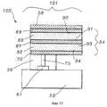
Фиг. 3 представляет детальный вид в разрезе тонкопленочного приводимого в действие зеркала 51, показанного на фиг. 2. Активная матрица 52 включает подложку 59, матрицу из М•N транзисторов (не показана) и матрицу 60 из М•N соединительных выводов 61; каждая из тонкопленочных приводных структур 54 снабжается верхней и нижней поверхностями 61, 63, ближними и дальними краями и, кроме того, включает по меньшей мере один тонкопленочный слой 66 индуцирующего перемещение материала, имеющего верхнюю и нижнюю поверхности 67, 68 и первый и второй электроды 69, 70 определенной толщины, выполненные, например, из такого металла, как золото (Au) или серебра (Ag), причем первый электрод 69 имеет верхнюю поверхность 39. Первый электрод 69 расположен на верхней поверхности 67 индуцирующего перемещение тонкопленочного слоя 66 и второй электрод 70 на его нижней поверхности 68. Индуцирующий перемещение тонкопленочный слой 66 выполнен полнен из электрострикционного материала, магнитострикционного материала или пьезоэлектрического материала. FIG. 3 is a detailed sectional view of a thin film actuated
В случае, когда индуцирующий перемещение слой выполнен из пьезоэлектрической керамики или пьезоэлектрического полимера, он должен быть поляризован. In the case where the displacement-inducing layer is made of piezoelectric ceramics or a piezoelectric polymer, it must be polarized.
Каждый из М•N поддерживающих элементов 56, снабженных верхней и нижней поверхностями 71, 72, используются для фиксации каждой из приводных структур 54, а также для электрического соединения второго электрода 70 в каждой из приводных структур 54 с соответствующими соединительными выводами 61 активной матрице 52 с помощью снабжения перемычкой 73, выполненной из электропроводящего материала, например, металла. В этой изобретенной матрице 50 из М•N тонкопленочных приводимых в действие зеркал 51 каждая из приводных структур 54 выступает в виде консоли от каждого из поддерживающих элементов 56, путем ее помещения на верхнюю поверхность 71 каждого из поддерживающих элементов 56 нижней поверхностью 63 каждой из приводных структур 54 и ее ближнего края 64, а нижняя поверхность 72 каждого из поддерживающих элементов 56 помещена на верхнюю поверхность активной матрицы 52. Каждое из М•N зеркал 58 для отражения световых лучей расположено на верхней поверхности каждой из приводных структур 54. Электрический сигнал приложен к индуцирующему перемещение тонкопленочному слою 66 между первым и вторым электродами 69, 70 в каждой из приводных структур 54. Приложение такого электрического сигнала вызывает деформацию индуцирующего перемещение слоя 66, следовательно, приводной структуры 54 и, следовательно, зеркала 58, расположенного на его верхней поверхности. Each of the M •
Для того, чтобы матрица 50 из MxN тонкопленочных приводимых в действие зеркал 51 правильно функционировала, общая толщина зеркала 58 и первого электрода 69 в каждом из тонкопленочных приводимых в действие зеркал 51 должна быть отлична от толщины второго электрода для того, чтобы имела место деформация. В противном случае упругий слой 88, имеющий верхнюю поверхность 40, должен быть дополнительно обеспечен к каждому из приводимых в действие зеркал 51. Упругий слой 88 может быть расположен либо между зеркалом 58 и первым электродом 69, либо на нижней поверхности второго электрода 70 в каждом из приводимых в действие зеркал 51, как изображено на фиг. 4 и 5. In order for the
Электрически проводящий материал, покрывающий первый электрод 69, должен быть также светоотражающим, например, алюминий (A1), который позволит верхней поверхности 39 первого электрода действовать так же, как зеркало 58 в каждом из тонкопленочных приводимых в действие зеркал 51. В таком случае, для того, чтобы каждое из тонкопленочных приводимых в действие зеркал 51 правильно функционировало, первый и второй электроды 69, 70 должны быть различной толщины или каждое из тонкопленочных приводимых в действие зеркал 51 должно быть обеспечено упругим слоем 88, расположенным на нижней поверхности каждой из приводных структур, как показано на фиг. 6 и 7. Более того, если упругий слой 88 выполнен из светоотражающего материала, он может также действовать, как зеркало 58, как изображено на фиг. 8. The electrically conductive material covering the
Возможно для изобретенной матрицы 50 тонкопленочных приводимых в действие зеркал 51 одинаково хорошо функционировать при наличии верхней и нижней поверхностей 67, 68 индуцирующего перемещение тонкопленочного слоя в каждой из приводных структур 54, покрытых полностью первым и вторым электродами 69, 70, либо верхняя поверхность индуцирующего перемещение тонкопленочного слоя 66, частично покрытая первым электродом 69, или нижняя поверхность 70 индуцирующего перемещение тонкопленочного слоя, частично покрытая вторым электродом 70. Два примера приводимого в действие зеркала, имеющего такую структуру, иллюстрируются на фиг. 9A и 9B. It is possible for the invented
В качестве примера первого воплощения, на фиг. 8 и 10 иллюстрируется матрица 50 из M•N тонкопленочных приводимых в действие зеркал 51, содержащая матрицу из М•N приводимых структур 54, выполненных из пьезокристаллической керамики, например, из цирконат-титанат свинца (ЦТС). Электрическое поле прикладывается к индуцирующему перемещение тонкопленочному пьезоэлектрическому слою 66, расположенному между первым и вторым электродами 69, 70 в каждой из приводных структур 54. Приложение электрического поля будет вызывать либо сжатие, либо расширение пьезоэлектрической керамики в зависимости от полярности электрического поля относительно полярности пьезоэлектрического материала. Если полярность электрического поля соответствует полярности пьезоэлектрической керамики, пьезоэлектрическая керамика будет сжиматься. Если полярность электрического поля противоположна полярности пьезоэлектрической керамики, пьезоэлектрическая керамика будет расширяться. As an example of the first embodiment, in FIG. 8 and 10 illustrate a
Ссылаясь на фиг. 8 и 10, полярность пьезоэлектрической керамики соответствует полярности приложенного электрического поля, вызывая сжатие пьезоэлектрической керамики. Referring to FIG. 8 and 10, the polarity of the piezoelectric ceramic corresponds to the polarity of the applied electric field, causing compression of the piezoelectric ceramic.
Так как упругий слой 88 не сжимается, приводная структура изгибается вниз, как показано на фиг. 10. Обратимся теперь к фиг. 8 и 10, можно показать, что свет, столкнувшись с верхней поверхностью 40 упругого слоя 88, действующего как зеркало 58 приводимого в действие зеркала 51, показанного на фиг. 10, отражается под большим углом, чем свет, отраженный от неприведенного в действие приводимого в действие зеркала 51, показанного на фиг. 8. Since the
Наоборот, электрическое поле обратной полярности может быть приложено к индуцирующему перемещение тонкопленочному пьезоэлектрическому слою 66, вызывая расширение пьезоэлектрической керамики. В этом примере упругий слой 88 не расширяется, и в результате приводная структура 54 изгибается вверх (не показано). Conversely, an electric field of reverse polarity can be applied to the displacement-inducing thin-
Свет, столкнувшись с зеркалом 58 перемещенного вверх приведенного в действие зеркала 51, отражается под меньшим углом, чем свет, отраженный от верхней поверхности 40 упругого слоя 88 неприведенного в действие приводимого в действие зеркала 51, показанного на фиг. 8. Light colliding with the
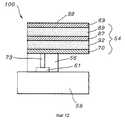
На фиг. 11 показан вид в разрезе второго воплощения матрицы 100 из М•N тонкопленочных приводимых в действие зеркал 101, где второе воплощение аналогично первому воплощению за исключением того, что каждая из приводных структур 54 является биморфной структурой, включающей первый электрод 69, второй электрод 70, промежуточные металлические слои 87, верхний индуцирующий перемещение тонкопленочный слой 89, имеющий верхнюю и нижние поверхности 90, 91, и нижний индуцирующий перемещение тонкопленочный слой 92, снабженный верхней и нижней поверхностями 93, 94. В каждой из приведенных структур 54, верхний и нижний индуцирующие перемещение тонкопленочные слои 89, 92 разделены промежуточным металлическим слоем 87, первый электрод 69 расположен на верхней поверхности 90 верхнего индуцирующего перемещение тонкопленочного слоя 89, а второй электрод 70 - на нижней поверхности 94 нижнего индуцирующего перемещение тонкопленочного слоя 92. In FIG. 11 is a cross-sectional view of a second embodiment of a
Так же как в случае первого воплощения, верхний и нижний индуцирующие перемещение тонкопленочные слои 85, 92 в каждой из приводных структур 54 выполнены из пьезоэлектрической керамики, электрострикционной керамики, магнитострикционной керамики или пьезоэлектрического полимера. As in the case of the first embodiment, the upper and lower displacement-inducing thin film layers 85, 92 in each of the
В случае, когда верхний и нижний индуцирующие перемещение тонкопленочные слои 89, 92 выполнены из пьезоэлектрической керамики или пьезоэлектрического полимера, верхний и нижний индуцирующие перемещение тонкопленочные слои 89, 92 должны быть поляризованы таким образом, чтобы направление поляризации пьезоэлектрического материала в верхнем индуцирующем перемещение тонкопленочном слое 89 было противоположно направлению поляризации нижнего индуцирующего перемещение тонкопленочного слоя 92. In the case where the upper and lower displacement-inducing thin-film layers 89, 92 are made of piezoelectric ceramics or a piezoelectric polymer, the upper and lower displacement-inducing thin-film layers 89, 92 should be polarized so that the direction of polarization of the piezoelectric material in the upper displacement-inducing thin-
Фиг. 12 иллюстрирует вид в разрезе приводимого в действие зеркала 101 второго воплощения, где первый электрод 69 выполнен из светоотражающего материала, таким образом позволяя его верхней поверхности так же действовать, как зеркало 58. FIG. 12 illustrates a cross-sectional view of an actuated
В качестве примера, как функционирует второе воплощение, предположим, что верхний и нижний индуцирующие перемещение тонкопленочные слои 89, 92 в матрице 100 из M•N тонкопленочных приводимых в действие зеркал 101, показанной на фиг. 11, выполнены из пьезоэлектрической керамики, например ЦТС. Когда электрическое поле прикладывается к каждой из приводных структур 54, верхнего и нижнего индуцирующих перемещение тонкопленочных пьезоэлектрических слоев 89, 92 приводная структура 54 будет изгибаться либо вверх, либо вниз, в зависимости от поляризации пьезоэлектрической керамики и полярности электрического поля. Например, если полярность вызывает сжатие верхнего индуцирующего перемещение тонкопленочного пьезоэлектрического слоя 89, а нижнего индуцирующего перемещение тонкопленочного пьезоэлектрического слоя 92 - расширение, приводная структура 54 будет изгибаться вверх. В этой ситуации ударяющийся свет отражается на меньший угол от приводной структуры 54, чем отраженный свет от не приведенной в действие приводной структуры 54. Однако, если полярность пьезоэлектрической керамики и электрическое поле вызывают расширение верхнего индуцирующего перемещение тонкопленочного пьезоэлектрического слоя 89, а нижнего индуцирующего перемещение тонкопленочного пьезоэлектрического слоя 92 - сжатие, приводная структура 54 будет изгибаться вниз. В этой ситуации ударяющийся свет отражается под большим углом от приводной структуры 54, чем отраженный свет от неприведенной в действие приводной структуры 54. As an example of how the second embodiment functions, suppose that the upper and lower displacement-inducing thin film layers 89, 92 in the
На фиг. 13A-13F проиллюстрированы шаги изготовления, входящие в изготовление первого воплощения настоящего изобретения. Процесс изготовления первого воплощения, то есть матрица 50 из M•N тонкопленочных приводимых в действие зеркал 51, где М и N - целые числа, начинается с подготовки активной матрицы 52, имеющей верхнюю и нижнюю поверхности 75, 76, содержащей подложку 59, матрицу из M•N транзисторов (не показана) и матрицу 60 из M•N соединительных выводов 61, как проиллюстрировано на фиг. 13A. In FIG. 13A-13F illustrate manufacturing steps involved in manufacturing the first embodiment of the present invention. The manufacturing process of the first embodiment, that is, the
На последующем шаге на верхней поверхности 75 активной матрицы 52 формируется поддерживающий слой 80, включающий избыточную область 83 и матрицу 81 из M•N опорных стоек 82, соответствующих матрице 55 из M•N поддерживающих элементов 56, где поддерживающий слой 80 формируется путем: напыления избыточного слоя (не показан) на всю верхнюю поверхность 75 активной матрицы 52; формирования матрицы из M•N пустых гнезд (не показана) в таким образом полученную избыточную область 83, причем каждое из пустых гнезд расположено вокруг каждого из M•N соединительных выводов 61: и обеспечения опорных стоек 82 в каждом из пустых гнезд, как показано на фиг. 13B. Избыточный слой формируется с использованием способа металлизации, матрица пустых гнезд - с использованием способа травления, а опорных стоек - с использованием металлизации или способа химического осаждения паров, с последующим способом травления. Избыточная область 83 поддерживающего слоя 80 затем обрабатывается так, чтобы ее можно было впоследствии удалить, используя способ травления или применения химикатов. In a subsequent step, a
Перемычка 73 для электрического соединения каждого из соединительных выводов 61 с каждым из вторых электродов 70, выполняемая из электрически проводящего материала, например вольфрама (W), формируется в каждой из опорных стоек 82 путем первоначального создания отверстия, распространяющегося от ее верхней поверхности до верхней поверхности соответствующих соединительных выводов 61 с использованием способа травления, с последующим наполнением отверстия электрически проводящим материалом, как изображено на фиг. 13C. A
На последующем шаге, как изображено на фиг. 13D, первый тонкопленочный электродный слой 84, выполненный из электрически проводящего материала, например, серебра (Ag), напыляется на поддерживающий слой 80. Затем тонкопленочный индуцирующий перемещение слой 85, выполненный из индуцирующего перемещение материала, например, из цирконат-титанат свинца (ЦТС), и второй тонкопленочный электродный слой 95 соответственно формируется на первом тонкопленочном электродном слое 84. In the next step, as shown in FIG. 13D, a first thin
Впоследствии, тонкопленочный слой 99 из соответствующего материала, например, алюминия (Al), обеспечивается на верхней поверхности второго тонкопленочного электродного слоя 95. Subsequently, a
Тонкопленочные слон электрически проводящих, индуцирующих перемещение и светоотражающих материалов могут быть напылены и сформированы с помощью известных тонкопленочных технологий, таких, как металлизация, конденсация, испарение, химическое осаждение паров, травление и микрообработка на станке, как показано на фиг. 13Е. Thin film elephants of electrically conductive, motion inducing and reflective materials can be sprayed and formed using known thin film technologies such as metallization, condensation, evaporation, chemical vapor deposition, etching and microprocessing on a machine, as shown in FIG. 13E.
Избыточная область 83 поддерживающего слоя 80 затем удаляется или растворяется с помощью применения химических реактивов для того, чтобы сформировать матрицу 50 из M•N тонкопленочных приводимых в действие зеркал 51, как проиллюстрировано на фиг. 13F. The
Второе воплощение изготовляется аналогичным способом, как первое воплощение. Поддерживающий слой прикладывается к активной матрице. Поддерживающий слой также включает избыточную область и матрицу из М•N опорных стоек, соответствующих матрице из M•N поддерживающих элементов. Первый тонкопленочный электродный слой затем осаждают на несущий слой. Затем нижний индуцирующий перемещение слой, промежуточный металлический слой и верхний индуцирующий перемещение слой формируют последовательно сверху первого тонкопленочного электродного слоя. Затем второй тонкопленочный электродный слой осаждают сверху верхнего индуцирующего перемещение слоя. Тонкопленочные слои электрически проводящих, индуцирующих перемещение и светоотражающих материалов могут быть напылены и сформированы с помощью известных тонкопленочных технологий, как указано ранее. Избыточная область поддерживающего слоя растворяется или удаляется с помощью применения химических реактивов, оставляя матрицу 100 тонкопленочных приводимых в действие зеркал 101, имеющей матрицу 53 из М•N приводных структур 54 с биморфной структурой, причем каждая из приводных структур 54 выступает в виде консоли от каждого из поддерживающих элементов 56. The second embodiment is manufactured in a similar manner as the first embodiment. A support layer is applied to the active matrix. The support layer also includes an excess region and an array of M • N support legs corresponding to an array of M • N support elements. The first thin film electrode layer is then deposited on the carrier layer. Then, the lower displacement-inducing layer, the intermediate metal layer and the upper displacement-inducing layer are formed sequentially on top of the first thin-film electrode layer. Then, the second thin film electrode layer is deposited on top of the upper displacement inducing layer. Thin film layers of electrically conductive, motion inducing, and retroreflective materials can be sprayed and formed using known thin film technologies, as previously indicated. The excess region of the support layer is dissolved or removed by the use of chemicals, leaving a
В вышеописанных способах изготовления первого и второго воплощения настоящего изобретения может быть добавлен дополнительный процесс для формирования упругого слоя 88, включающий в себя аналогичный процесс, как при формировании других тонкопленочных слоев. In the above-described manufacturing methods of the first and second embodiments of the present invention, an additional process for forming the
Несмотря на то, что настоящее изобретение было описано относительно только определенных предпочтительных воплощений, другие модификации и изменения могут быть сделаны не выходя за рамки настоящего изобретения, как излагается в формуле изобретения. Although the present invention has been described with respect to only certain preferred embodiments, other modifications and changes can be made without departing from the scope of the present invention as set forth in the claims.
Claims (33)
Translated fromRussian29.10.93 по пп.1-6, 8, 9, 11, 14, 16-19;
30.11.93 по пп.7, 15, 20 и 21;
30.12.93 по пп.10, 12 и 13;
16.11.93 по пп.22-33.Priority on points:
10.29.93 according to claims 1-6, 8, 9, 11, 14, 16-19;
11/30/93 according to claims 7, 15, 20 and 21;
12/30/93 according to claims 10, 12 and 13;
11.16.93 according to claims 22-33.
Applications Claiming Priority (9)
| Application Number | Priority Date | Filing Date | Title |
|---|---|---|---|
| KR1019930022798AKR970006685B1 (en) | 1993-10-29 | 1993-10-29 | Light Path Control |
| KR93-22798 | 1993-10-29 | ||
| KR93-24398 | 1993-11-16 | ||
| KR93024398AKR970006694B1 (en) | 1993-11-16 | 1993-11-16 | A manufacturing method of an optical path regulating apparatus |
| KR1019930025879AKR970006698B1 (en) | 1993-11-30 | 1993-11-30 | An optical path regulating apparatus |
| KR93-25879 | 1993-11-30 | ||
| KR1019930031720AKR970008404B1 (en) | 1993-12-30 | 1993-12-30 | Optical path adjuster of projection image display device |
| KR93-31720 | 1993-12-30 | ||
| PCT/KR1994/000148WO1995012287A1 (en) | 1993-10-29 | 1994-10-25 | Thin film actuated mirror array and methods for its manufacture |
Publications (2)
| Publication Number | Publication Date |
|---|---|
| RU96110182A RU96110182A (en) | 1998-08-10 |
| RU2140722C1true RU2140722C1 (en) | 1999-10-27 |
Family
ID=27483016
Family Applications (1)
| Application Number | Title | Priority Date | Filing Date |
|---|---|---|---|
| RU96110182/09ARU2140722C1 (en) | 1993-10-29 | 1994-10-25 | Thin-film actuated mirror matrix and process of its manufacture |
Country Status (16)
| Country | Link |
|---|---|
| US (2) | US5661611A (en) |
| EP (1) | EP0651274B1 (en) |
| JP (1) | JP3283881B2 (en) |
| CN (1) | CN1047056C (en) |
| AU (1) | AU693119B2 (en) |
| BR (1) | BR9407923A (en) |
| CA (1) | CA2175198A1 (en) |
| CZ (1) | CZ288846B6 (en) |
| DE (1) | DE69420666T2 (en) |
| ES (1) | ES2140490T3 (en) |
| HU (1) | HU220516B1 (en) |
| MY (1) | MY113977A (en) |
| PL (1) | PL176406B1 (en) |
| RU (1) | RU2140722C1 (en) |
| TW (1) | TW279930B (en) |
| WO (1) | WO1995012287A1 (en) |
Families Citing this family (23)
| Publication number | Priority date | Publication date | Assignee | Title |
|---|---|---|---|---|
| US5936757A (en)* | 1993-10-29 | 1999-08-10 | Daewoo Electronics Co., Ltd. | Thin film actuated mirror array |
| RU2140722C1 (en)* | 1993-10-29 | 1999-10-27 | Дэу Электроникс Ко., Лтд. | Thin-film actuated mirror matrix and process of its manufacture |
| US6969635B2 (en)* | 2000-12-07 | 2005-11-29 | Reflectivity, Inc. | Methods for depositing, releasing and packaging micro-electromechanical devices on wafer substrates |
| TW348324B (en)* | 1996-01-31 | 1998-12-21 | Daewoo Electronics Co Ltd | Thin film actuated mirror array having dielectric layers |
| IL127391A0 (en)* | 1996-06-05 | 1999-10-28 | Remote Source Lighting Int Inc | Large-area fiber optic display using piezoelectric shutters |
| BE1010327A7 (en)* | 1996-06-05 | 1998-06-02 | Remote Source Lighting Int Inc | MODULATION DEVICE, ELECTRO-OPTICAL LIGHT INCLUDING bimorphs. |
| WO1998008127A1 (en)* | 1996-08-21 | 1998-02-26 | Daewoo Electronics Co., Ltd. | Thin film actuated mirror array for use in an optical projection system |
| WO1998033327A1 (en)* | 1997-01-23 | 1998-07-30 | Daewoo Electronics Co., Ltd. | Thin film actuated mirror array in an optical projection system and method for manufacturing the same |
| CA2278624A1 (en)* | 1997-01-23 | 1998-07-30 | Daewoo Electronics Co., Ltd. | Thin film actuated mirror array in an optical projection system and method for manufacturing the same |
| RU2180158C2 (en)* | 1997-01-23 | 2002-02-27 | Дэу Электроникс Ко., Лтд. | Thin-film matrix of controlled mirrors for optical projection system and its manufacturing process |
| WO1998038801A1 (en)* | 1997-02-26 | 1998-09-03 | Daewoo Electronics Co., Ltd. | Thin film actuated mirror array in an optical projection system and method for manufacturing the same |
| US5815305A (en)* | 1997-03-10 | 1998-09-29 | Daewoo Electronics Co., Ltd. | Thin film actuated mirror array in an optical projection system and method for manufacturing the same |
| KR19990004774A (en)* | 1997-06-30 | 1999-01-25 | 배순훈 | Manufacturing method of thin film type optical path control device |
| DE10031877C1 (en)* | 2000-06-30 | 2001-12-20 | Fraunhofer Ges Forschung | Device for deflecting optical rays |
| JP2002122809A (en)* | 2000-10-18 | 2002-04-26 | Canon Inc | Projection display device |
| US6647164B1 (en) | 2000-10-31 | 2003-11-11 | 3M Innovative Properties Company | Gimbaled micro-mirror positionable by thermal actuators |
| US6711318B2 (en) | 2001-01-29 | 2004-03-23 | 3M Innovative Properties Company | Optical switch based on rotating vertical micro-mirror |
| US6624549B2 (en)* | 2001-03-02 | 2003-09-23 | Ngk Insulators, Ltd. | Piezoelectric/electrostrictive device and method of fabricating the same |
| US6721510B2 (en)* | 2001-06-26 | 2004-04-13 | Aoptix Technologies, Inc. | Atmospheric optical data transmission system |
| DE10150424B4 (en)* | 2001-10-11 | 2004-07-29 | Siemens Ag | Reflection system and use of the reflection system |
| US7281808B2 (en)* | 2003-06-21 | 2007-10-16 | Qortek, Inc. | Thin, nearly wireless adaptive optical device |
| WO2017171882A1 (en)* | 2016-04-01 | 2017-10-05 | Intel Corporation | Piezoelectrically actuated mirrors for optical communications |
| CN114779464A (en)* | 2022-05-24 | 2022-07-22 | 北京有竹居网络技术有限公司 | Optical signal modulator, control method and projection device |
Citations (2)
| Publication number | Priority date | Publication date | Assignee | Title |
|---|---|---|---|---|
| US5085497A (en)* | 1990-03-16 | 1992-02-04 | Aura Systems, Inc. | Method for fabricating mirror array for optical projection system |
| EP0550022A2 (en)* | 1991-12-31 | 1993-07-07 | Texas Instruments Incorporated | Light beam steering with deformable membrane device |
Family Cites Families (32)
| Publication number | Priority date | Publication date | Assignee | Title |
|---|---|---|---|---|
| US2016962A (en)* | 1932-09-27 | 1935-10-08 | Du Pont | Process for producing glucamines and related products |
| US1985424A (en)* | 1933-03-23 | 1934-12-25 | Ici Ltd | Alkylene-oxide derivatives of polyhydroxyalkyl-alkylamides |
| US2290529A (en)* | 1941-08-23 | 1942-07-21 | Sr Frank J Black | Device for measuring rotating workpieces |
| US2703798A (en)* | 1950-05-25 | 1955-03-08 | Commercial Solvents Corp | Detergents from nu-monoalkyl-glucamines |
| US3614677A (en)* | 1966-04-29 | 1971-10-19 | Ibm | Electromechanical monolithic resonator |
| US3544201A (en)* | 1968-01-02 | 1970-12-01 | Gen Telephone & Elect | Optical beam deflector |
| US3758199A (en)* | 1971-11-22 | 1973-09-11 | Sperry Rand Corp | Piezoelectrically actuated light deflector |
| US4441791A (en)* | 1980-09-02 | 1984-04-10 | Texas Instruments Incorporated | Deformable mirror light modulator |
| US4518976A (en)* | 1982-11-17 | 1985-05-21 | Konishiroku Photo Industry Co., Ltd. | Recording apparatus |
| US4529620A (en)* | 1984-01-30 | 1985-07-16 | New York Institute Of Technology | Method of making deformable light modulator structure |
| DE3720469A1 (en)* | 1987-06-20 | 1988-12-29 | Bernd Dipl Ing Haastert | Liquid-crystal light valve |
| US4932119A (en)* | 1989-03-28 | 1990-06-12 | Litton Systems, Inc. | Method of making standard electrodisplacive transducers for deformable mirrors |
| US4947487A (en)* | 1989-05-04 | 1990-08-14 | The Jackson Laboratory | Laser beam protective gloves |
| US4979789A (en)* | 1989-06-02 | 1990-12-25 | Aura Systems, Inc. | Continuous source scene projector |
| US5032906A (en)* | 1989-07-12 | 1991-07-16 | Aura Systems, Inc. | Intensity calibration method for scene projector |
| US4954789A (en)* | 1989-09-28 | 1990-09-04 | Texas Instruments Incorporated | Spatial light modulator |
| US5126836A (en)* | 1989-11-01 | 1992-06-30 | Aura Systems, Inc. | Actuated mirror optical intensity modulation |
| US5245369A (en)* | 1989-11-01 | 1993-09-14 | Aura Systems, Inc. | Scene projector |
| US5260798A (en)* | 1989-11-01 | 1993-11-09 | Aura Systems, Inc. | Pixel intensity modulator |
| US5150205A (en)* | 1989-11-01 | 1992-09-22 | Aura Systems, Inc. | Actuated mirror optical intensity modulation |
| US5185660A (en)* | 1989-11-01 | 1993-02-09 | Aura Systems, Inc. | Actuated mirror optical intensity modulation |
| US5035475A (en)* | 1990-03-15 | 1991-07-30 | Aura Systems, Inc. | Unique modulation television |
| US5138309A (en)* | 1990-04-03 | 1992-08-11 | Aura Systems, Inc. | Electronic switch matrix for a video display system |
| US5175465A (en)* | 1991-10-18 | 1992-12-29 | Aura Systems, Inc. | Piezoelectric and electrostrictive actuators |
| US5159225A (en)* | 1991-10-18 | 1992-10-27 | Aura Systems, Inc. | Piezoelectric actuator |
| US5247222A (en)* | 1991-11-04 | 1993-09-21 | Engle Craig D | Constrained shear mode modulator |
| US5233456A (en)* | 1991-12-20 | 1993-08-03 | Texas Instruments Incorporated | Resonant mirror and method of manufacture |
| US5212582A (en)* | 1992-03-04 | 1993-05-18 | Texas Instruments Incorporated | Electrostatically controlled beam steering device and method |
| US5488505A (en)* | 1992-10-01 | 1996-01-30 | Engle; Craig D. | Enhanced electrostatic shutter mosaic modulator |
| US5510824A (en)* | 1993-07-26 | 1996-04-23 | Texas Instruments, Inc. | Spatial light modulator array |
| RU2140722C1 (en)* | 1993-10-29 | 1999-10-27 | Дэу Электроникс Ко., Лтд. | Thin-film actuated mirror matrix and process of its manufacture |
| US5481396A (en)* | 1994-02-23 | 1996-01-02 | Aura Systems, Inc. | Thin film actuated mirror array |
- 1994
- 1994-10-25RURU96110182/09Apatent/RU2140722C1/ennot_activeIP Right Cessation
- 1994-10-25CZCZ19961180Apatent/CZ288846B6/ennot_activeIP Right Cessation
- 1994-10-25AUAU80052/94Apatent/AU693119B2/ennot_activeCeased
- 1994-10-25PLPL94314124Apatent/PL176406B1/enunknown
- 1994-10-25JPJP51252995Apatent/JP3283881B2/ennot_activeExpired - Fee Related
- 1994-10-25HUHU9601094Apatent/HU220516B1/ennot_activeIP Right Cessation
- 1994-10-25CNCN94193967Apatent/CN1047056C/ennot_activeExpired - Lifetime
- 1994-10-25WOPCT/KR1994/000148patent/WO1995012287A1/enactiveIP Right Grant
- 1994-10-25BRBR9407923Apatent/BR9407923A/ennot_activeIP Right Cessation
- 1994-10-25CACA002175198Apatent/CA2175198A1/ennot_activeAbandoned
- 1994-10-28USUS08/331,399patent/US5661611A/ennot_activeExpired - Lifetime
- 1994-10-28MYMYPI94002871Apatent/MY113977A/enunknown
- 1994-10-28DEDE69420666Tpatent/DE69420666T2/ennot_activeExpired - Lifetime
- 1994-10-28EPEP94117124Apatent/EP0651274B1/ennot_activeExpired - Lifetime
- 1994-10-28ESES94117124Tpatent/ES2140490T3/ennot_activeExpired - Lifetime
- 1994-11-03TWTW083110157Apatent/TW279930B/zhactive
- 1997
- 1997-06-17USUS08/877,084patent/US5900998A/ennot_activeExpired - Lifetime
Patent Citations (2)
| Publication number | Priority date | Publication date | Assignee | Title |
|---|---|---|---|---|
| US5085497A (en)* | 1990-03-16 | 1992-02-04 | Aura Systems, Inc. | Method for fabricating mirror array for optical projection system |
| EP0550022A2 (en)* | 1991-12-31 | 1993-07-07 | Texas Instruments Incorporated | Light beam steering with deformable membrane device |
Non-Patent Citations (1)
| Title |
|---|
| Лабунов В.А. и др. Ионно-лучевые источники для обработки поверхности твердых тел и получения тонких пленок. Зарубежная электронная техника. - М.: Министерство электронной промышленности, 1982, с.9-14.* |
Also Published As
| Publication number | Publication date |
|---|---|
| AU8005294A (en) | 1995-05-22 |
| WO1995012287A1 (en) | 1995-05-04 |
| CN1134208A (en) | 1996-10-23 |
| PL314124A1 (en) | 1996-08-19 |
| JP3283881B2 (en) | 2002-05-20 |
| EP0651274B1 (en) | 1999-09-15 |
| HU220516B1 (en) | 2002-03-28 |
| US5900998A (en) | 1999-05-04 |
| ES2140490T3 (en) | 2000-03-01 |
| EP0651274A1 (en) | 1995-05-03 |
| US5661611A (en) | 1997-08-26 |
| PL176406B1 (en) | 1999-05-31 |
| CA2175198A1 (en) | 1995-05-04 |
| CZ118096A3 (en) | 1996-09-11 |
| DE69420666D1 (en) | 1999-10-21 |
| MY113977A (en) | 2002-07-31 |
| HU9601094D0 (en) | 1996-07-29 |
| JPH09504387A (en) | 1997-04-28 |
| BR9407923A (en) | 1996-11-26 |
| HUT75803A (en) | 1997-05-28 |
| TW279930B (en) | 1996-07-01 |
| AU693119B2 (en) | 1998-06-25 |
| DE69420666T2 (en) | 1999-12-30 |
| CN1047056C (en) | 1999-12-01 |
| CZ288846B6 (en) | 2001-09-12 |
Similar Documents
| Publication | Publication Date | Title |
|---|---|---|
| RU2140722C1 (en) | Thin-film actuated mirror matrix and process of its manufacture | |
| RU2141175C1 (en) | Thin-film actuating mirror matrix for its use in optical projection system and method for its manufacturing | |
| RU2125347C1 (en) | Array of thin-film controlled reflectors for optical projection system and its manufacturing process | |
| KR100218826B1 (en) | Thin film actuated mirror array | |
| RU96112195A (en) | THIN FILM OPERATED MIRROR MATRIX FOR USE IN OPTICAL PROJECTION SYSTEM AND METHOD FOR ITS MANUFACTURE | |
| RU2129759C1 (en) | Periodic structure of drive-coupled thin-film mirrors for optical projection systems and its manufacturing process | |
| US5735026A (en) | Method for the manufacture of an electrodisplacive actuator array | |
| US5585956A (en) | Electrostrictive actuated mirror array | |
| US5936757A (en) | Thin film actuated mirror array | |
| AU703795B2 (en) | Low temperature formed thin film actuated mirror array | |
| US5768008A (en) | Actuator array and method for the manufacture thereof | |
| KR19990018830A (en) | Thin film type optical path control device capable of improving driving angle |
Legal Events
| Date | Code | Title | Description |
|---|---|---|---|
| MM4A | The patent is invalid due to non-payment of fees | Effective date:20031026 |