RU2134468C1 - Process and device to test semiconductor structure - Google Patents
Process and device to test semiconductor structureDownload PDFInfo
- Publication number
- RU2134468C1 RU2134468C1RU97116300ARU97116300ARU2134468C1RU 2134468 C1RU2134468 C1RU 2134468C1RU 97116300 ARU97116300 ARU 97116300ARU 97116300 ARU97116300 ARU 97116300ARU 2134468 C1RU2134468 C1RU 2134468C1
- Authority
- RU
- Russia
- Prior art keywords
- analyzer
- detector
- control electrode
- energy
- probe
- Prior art date
Links
- 238000000034methodMethods0.000titleclaimsabstractdescription14
- 239000004065semiconductorSubstances0.000titleclaimsabstractdescription11
- 238000012360testing methodMethods0.000titleabstractdescription5
- 239000000523sampleSubstances0.000claimsabstractdescription39
- 230000003287optical effectEffects0.000claimsabstractdescription26
- 230000005855radiationEffects0.000claimsabstractdescription25
- 238000005259measurementMethods0.000claimsabstractdescription11
- 238000007654immersionMethods0.000claimsabstractdescription6
- 238000005286illuminationMethods0.000claimsabstractdescription4
- 230000001360synchronised effectEffects0.000claimsdescription19
- 239000000463materialSubstances0.000claimsdescription6
- 230000001678irradiating effectEffects0.000claimsdescription3
- 230000001747exhibiting effectEffects0.000claims1
- 230000000694effectsEffects0.000abstractdescription2
- 230000004907fluxEffects0.000abstractdescription2
- 230000015572biosynthetic processEffects0.000abstract1
- 239000000126substanceSubstances0.000abstract1
- 238000010586diagramMethods0.000description9
- 238000012806monitoring deviceMethods0.000description6
- 239000002800charge carrierSubstances0.000description4
- ZOXJGFHDIHLPTG-UHFFFAOYSA-NBoronChemical compound[B]ZOXJGFHDIHLPTG-UHFFFAOYSA-N0.000description1
- OAICVXFJPJFONN-UHFFFAOYSA-NPhosphorusChemical compound[P]OAICVXFJPJFONN-UHFFFAOYSA-N0.000description1
- XUIMIQQOPSSXEZ-UHFFFAOYSA-NSiliconChemical compound[Si]XUIMIQQOPSSXEZ-UHFFFAOYSA-N0.000description1
- 238000000137annealingMethods0.000description1
- 229910052796boronInorganic materials0.000description1
- 239000013078crystalSubstances0.000description1
- 230000007423decreaseEffects0.000description1
- 238000013461designMethods0.000description1
- 238000009826distributionMethods0.000description1
- 238000010894electron beam technologyMethods0.000description1
- 238000002513implantationMethods0.000description1
- 238000004519manufacturing processMethods0.000description1
- 239000011159matrix materialSubstances0.000description1
- 229910052698phosphorusInorganic materials0.000description1
- 239000011574phosphorusSubstances0.000description1
- 238000012545processingMethods0.000description1
- 230000035945sensitivityEffects0.000description1
- 229910052710siliconInorganic materials0.000description1
- 239000010703siliconSubstances0.000description1
Images
Landscapes
- Testing Or Measuring Of Semiconductors Or The Like (AREA)
Abstract
Description
Translated fromRussianИзобретение относится к области материаловедения, в частности к области бесконтактных измерений характеристик полупроводниковых структур, и может быть использовано для определения электрофизических параметров полупроводниковых структур, а также контроля топологии полупроводниковых структур на ранних этапах их изготовления. The invention relates to the field of materials science, in particular to the field of non-contact measurements of the characteristics of semiconductor structures, and can be used to determine the electrophysical parameters of semiconductor structures, as well as to control the topology of semiconductor structures in the early stages of their manufacture.
Известен способ определения электрических свойств полупроводников (US, патент 4902967), включающий облучение объекта электронным зондом и модулированным световым потоком с последующей регистрацией наведенной фотоЭДС на объекте. Недостатком данного способа следует признать низкую точность, вызванную неизвестным вкладом катодо-ЭДС в регистрируемый сигнал. Кроме того, измерение временных зависимостей фотоЭДС проводят при регистрации сигнала с выхода детектора вторичных электронов, имеющего ограниченный частотный диапазон. A known method for determining the electrical properties of semiconductors (US patent 4902967), including irradiating the object with an electronic probe and a modulated light stream, followed by registration of the induced photo-emf at the object. The disadvantage of this method is the low accuracy caused by the unknown contribution of the cathode-emf to the recorded signal. In addition, the measurement of the time dependences of the photoEMF is carried out when registering the signal from the output of the secondary electron detector, which has a limited frequency range.
Известен также способ определения электрофизических параметров полупроводников (SU, авторское свидетельство 1578770), включающий облучение объекта электронным зондом, измерение вторично-эмиссионного сигнала в режиме потенциального контраста, дополнительное освещение объекта равномерным по сечению потоком импульсного оптического излучения с энергией кванта, превышающей ширину запрещенной зоны материала объекта, измерение наведенной фотоЭДС и относительного значения обратных токов p-n-переходов, причем частоту и интенсивность следования импульсов устанавливают по выходу измеряемого сигнала в рабочую область. Для реализации способа предложено использовать устройство, содержащее зондовое устройство с отклоняющей системой, анализатор энергии вторичных электронов, расположенный наклонно относительно оси зондового устройства и включающий двухэлектродный иммерсионный объектив с коническими электродами и управляющий электрод, детектор вторичных электронов, источник оптического излучения, направленный на объект исследования и подключенный к генератору импульсов, видеоконтрольное устройство, соединенное к отклоняющей системой и выполненное с возможностью подключения к детектору вторичных электронов, усилитель, выполненный с возможностью подключения его выхода к управляющему электроду, синхронный детектор, выход которого подключен к видеоконтрольному устройству, измерительный вход - к управляющему электроду, а опорный вход - к генератору импульсов. Недостатком известного технического решения следует признать недостаточную точность измерения, вызванную неопределенностью вклада электронного зонда в фотоЭДС, относительно узкую область применения, а также недостаточную чувствительность. There is also a method for determining the electrophysical parameters of semiconductors (SU, copyright certificate 1578770), including irradiating an object with an electronic probe, measuring the secondary-emission signal in potential contrast mode, additional illumination of the object with a uniform cross-section of pulsed optical radiation with a quantum energy exceeding the band gap of the material object, measurement of induced photo-emf and the relative value of reverse currents of pn junctions, and the frequency and intensity of repetition I pulses set by the output of the measured signal in the work area. To implement the method, it is proposed to use a device containing a probe device with a deflecting system, a secondary electron energy analyzer, inclined relative to the axis of the probe device and including a two-electrode immersion lens with conical electrodes and a control electrode, a secondary electron detector, an optical radiation source aimed at the object of study and connected to a pulse generator, a video monitoring device connected to a deflecting system and executed can be connected to the secondary electron detector, amplifier, configured to connect its output to the control electrode, a synchronous detector, the output of which is connected to a monitoring device, a measuring input - to the control electrode, and a reference input - to the pulse generator. A disadvantage of the known technical solution should be recognized as insufficient measurement accuracy caused by the uncertainty of the contribution of the electron probe to the photo-emf, a relatively narrow scope, as well as insufficient sensitivity.
Техническая задача, решаемая настоящим изобретением, состоит в повышении информативности и точности способа определения электрофизических параметров. The technical problem solved by the present invention is to increase the information content and accuracy of the method for determining electrophysical parameters.
Технический результат, получаемый при реализации способа, состоит в повышении точности и быстродействии способа при одновременном увеличении числа определяемых параметров. The technical result obtained during the implementation of the method consists in increasing the accuracy and speed of the method while increasing the number of defined parameters.
Для получения указанного технического результата облучают поверхность полупроводникового объекта электронным зондом, регистрируют изображение его поверхности в режиме потенциального контраста с использованием анализатора энергии вторичных электронов, изменяют потенциал управляющего электрода анализатора и регистрируют изменение потенциального контраста отдельных областей объекта, выявляют области, подлежащие контролю, на основании величин изменения потенциального контраста, перемещают выявленные области в зону обработки электронно-зондового устройства при требуемом увеличении, дополнительно облучают поверхность объекта равномерным по сечению потоком оптического излучения с энергией кванта, превышающей ширину запрещенной зоны материала полупроводникового объекта при импульсной модуляции оптического излучения, измеряют наведенную фотоЭДС в режиме потенциального контраста, причем изменяют энергию и/или ток электронов зонда, и/или интенсивность оптического излучения в импульсе, и/или интенсивность оптического излучения в паузе между импульсами, и/или длительность, и/или частоту следования импульсов таким образом, чтобы зависимость измеряемой фотоЭДС при перечисленных параметрах электронного зонда и оптического излучения от параметров электронного зонда была слабой, а воздействие зонда на наведенную фотоЭДС минимальным, регистрируют распределения значений фотоЭДС по поверхности объекта, с использованием которых и определяют искомые электрофизические параметры объекта. To obtain the indicated technical result, the surface of the semiconductor object is irradiated with an electronic probe, the image of its surface is recorded in the potential contrast mode using a secondary electron energy analyzer, the potential of the control electrode of the analyzer is changed, and the potential contrast of individual areas of the object is recorded, the areas to be controlled are detected based on the values changes in potential contrast, move the identified areas to the processing zone at the required magnification, additionally irradiate the surface of the object with a uniform cross section of the optical radiation flux with a quantum energy exceeding the band gap of the semiconductor object material under pulsed modulation of optical radiation, measure the induced emf in the potential contrast mode, and change the energy and / or current probe electrons, and / or the intensity of optical radiation in a pulse, and / or the intensity of optical radiation in a pause between pulses, and / or for the intensity and / or pulse repetition rate so that the dependence of the measured photo emf with the listed parameters of the electron probe and optical radiation on the parameters of the electron probe is weak, and the effect of the probe on the induced photo emf is minimal, the distribution of photo emf values over the surface of the object is recorded, using which determine the desired electrophysical parameters of the object.
Область максимальных значений зависимости фотоЭДС от энергии и тока электронов зонда используют для контроля топологи планарных микрообластей. The region of maximum values of the dependence of photoEMF on the energy and current of the probe electrons is used to control topologies of planar microregions.
Монотонный участок зависимости фотоЭДС от энергии и тока электронов зонда используют для контроля топологии слоистых структур, в частности, легированных областей в изолированных карманах и/или структур, закрытых изолирующим или пассивирующим слоем. The monotonic plot of the dependence of the photoEMF on the energy and current of the probe electrons is used to control the topology of layered structures, in particular, doped regions in insulated pockets and / or structures covered by an insulating or passivating layer.
Квазилинейную область зависимости фотоЭДС от интенсивности оптического излучения и область максимальных значений зависимости фотоЭДС от энергии и тока электронов зонда используют для контроля неоднородностей электрофизических параметров структур, в частности, неоднородностей обратных токов или точек утечки p-n-переходов. The quasilinear region of the dependence of the photoEMF on the intensity of optical radiation and the region of the maximum dependence of the photoEMF on the energy and current of the probe electrons are used to control inhomogeneities of the electrophysical parameters of structures, in particular, inhomogeneities of reverse currents or leakage points of p-n junctions.
Окрестность граничной частоты зависимости фотоЭДС от частоты следования импульсов используют для измерения времени жизни неосновных носителей зарядов, при этом ограничивают область воздействия электронного зонда легированной областью объекта, а при регистрации зависимости фотоЭДС от частоты следования импульсов обеспечивают интенсивность оптического излучения в паузе между импульсами, энергию и ток электронов зонда такими, чтобы достичь насыщения граничной частоты, причем время жизни неосновных носителей заряда определяют с учетом кинетики фотоЭДС p-n-перехода, регистрируемой методом стробоскопии при подаче строб-импульсов на управляющий электрод анализатора. The neighborhood of the cutoff frequency of the dependence of the photoEMF on the pulse repetition rate is used to measure the lifetime of minority charge carriers, while limiting the area of influence of the electron probe by the doped region of the object, and when recording the dependence of the photoEMF on the pulse repetition rate, they provide the optical radiation intensity in the pause between pulses, energy and current the probe electrons in such a way as to achieve saturation of the cutoff frequency, and the lifetime of minority charge carriers is determined taking into account Ohm kinetics of the photo-emf of the p-n junction, recorded by the method of stroboscopy when applying strobe pulses to the control electrode of the analyzer.
Для реализации способа используют устройство, содержащее электронно-зондовое устройство с отклоняющей системой, анализатор энергии вторичных электронов порогового типа, расположенный наклонно относительно оси электронно-зондового устройства и включающий двухэлектродный иммерсионный объектив с коническими электродами и управляющий электрод, детектор вторичных электронов, источник оптического излучения, управляемый током, направленный на объект и соединенный с генератором импульсов, видеоконтрольное устройство, соединенное с отклоняющей системой и выполненное с возможностью подключения к детектору вторичных электронов, усилитель, выход которого подключен к управляемому электроду, синхронный детектор, выход которого подключен к видеоконтрольному устройству, измерительный вход - к управляющему электроду, а опорный вход - к генератору импульсов, причем дополнительно введенный управляемый источник напряжения постоянного тока подключен к суммирующему входу усилителя для управления анализатором энергии вторичных электронов, видеоконтрольное устройство подключено к генератору импульсов и выполнено с возможностью подключения к управляющему электроду анализатора энергии вторичных электронов и к опорному входу синхронного детектора, анализатор энергии вторичных электронов установлен наклонно относительно детектора электронов, иммерсионный объектив выполнен бездиафрагменным, а в качестве управляющего электрода использована диафрагма, установленная за ускоряющим электродом анализатора энергии вторичных электронов относительно входа анализатора. To implement the method, a device is used that contains an electron probe device with a deflecting system, a threshold-type secondary electron energy analyzer located obliquely relative to the axis of the electron probe device and including a two-electrode immersion lens with conical electrodes and a control electrode, a secondary electron detector, an optical radiation source, current-controlled, aimed at the object and connected to the pulse generator, a video monitoring device connected to the open a measuring system and configured to connect secondary electrons to the detector, an amplifier, the output of which is connected to a controlled electrode, a synchronous detector, the output of which is connected to a video monitoring device, a measuring input to a control electrode, and a reference input to a pulse generator, and additionally controlled input a DC voltage source is connected to the summing input of the amplifier to control the secondary electron energy analyzer, a video monitoring device is connected but to the pulse generator and is configured to connect the secondary electron energy analyzer to the control electrode and to the reference input of the synchronous detector, the secondary electron energy analyzer is mounted obliquely relative to the electron detector, the immersion lens is made diaphragmless, and the diaphragm mounted behind the accelerating electrode is used as the control electrode analyzer energy of secondary electrons relative to the input of the analyzer.
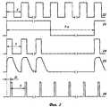
Изобретение иллюстрировано графическим материалом, где на фиг. 1 приведена блок-схема устройства, реализующего способ, а на фиг. 2 приведены диаграммы импульсов, используемые при измерении времени жизни неосновных носителей заряда. The invention is illustrated in graphic material, where in FIG. 1 is a block diagram of a device implementing the method, and FIG. Figure 2 shows the pulse diagrams used in measuring the lifetime of minority charge carriers.
Устройство, реализующее способ, содержит (фиг. 1) электронно-зондовое устройство 1 с вакуумной камерой для объектов, управляемый источник 2 высокого напряжения, управляемый источник 3 тока, отклоняющую систему 4, столик 5 для объекта, источник 6 оптического излучения, анализатор энергии вторичных электронов 7 порогового типа, ускоряющий электрод 8, диафрагменный управляющий электрод 9, детектор 10 вторичных электронов, усилитель 11 напряжения, управляемый источник 12 напряжения постоянного тока, генератор 13 импульсов, синхронный детектор 14, компьютер 15 с монитором и интерфейсом, используемый в качестве видеоконтрольного устройства, цилиндр Фарадея 16, измеритель 17 тока, задающий генератор 18, генератор 19 строб-импульсов, делитель 20 частоты, логический элемент 21. На фиг.2 приведены следующие диаграммы импульсов: с выхода задающего генератора 18 - диаграмма 22, с выхода делителя частоты 20 - диаграмма 23, с выхода генератора 13 - диаграмма 24, фотоЭДС объекта исследования - диаграмма 25, форма строб-импульсов с выхода генератора 19 - диаграмма 26. A device that implements the method comprises (Fig. 1) an electron probe device 1 with a vacuum chamber for objects, a controlled high voltage source 2, a controlled current source 3, a deflecting system 4, an object table 5, an optical radiation source 6, a secondary energy analyzer threshold-type electrons 7, accelerating electrode 8, diaphragm control electrode 9, secondary electron detector 10, voltage amplifier 11, controllable DC voltage source 12, pulse generator 13, synchronous detector 14, comp a yuter 15 with a monitor and an interface used as a video monitoring device, a Faraday cylinder 16, a current meter 17, a master oscillator 18, a strobe pulse generator 19, a frequency divider 20, a logic element 21. Figure 2 shows the following pulse diagrams: from the output the master oscillator 18 is a diagram 22, from the output of the frequency divider 20 is a diagram 23, from the output of the generator 13 is diagram 24, the photo-emf of the test object is diagram 25, the shape of the strobe pulses from the output of the oscillator 19 is diagram 26.
Ниже приведена конструкция устройства со ссылками на графический материал. Анализатор энергии вторичных электронов 7 установлен в камере объектов электронно-зондового устройства 1 наклонно относительно осей устройства 1 и детектора 10 вторичных электронов. Компьютер 15 соединен с отклоняющей системой 4, детектором 10 вторичных электронов и, кроме того, он может быть подключен к выходу синхронного детектора 14. Измерительный вход синхронного детектора 14 соединен с выходом усилителя 11 и может быть подключен к выходу детектора 10 вторичных электронов. Опорный вход синхронного детектора 14 соединен с генератором импульсов 13 и может быть подключен к делителю частоты 20. Вход усилителя 11 может быть подключен к детектору 10 вторичных электронов. Управляемый источник 12 напряжения постоянного тока соединен с суммирующим входом усилителя 11. Управляющий диафрагменный электрод 9 соединен с выходом усилителя 11 и может быть соединен с генератором 19 строб-импульсов. Генератор импульсов 13 соединен с источником 6 оптического излучения и может быть соединен со столиком 5. Задающий генератор 18 соединен с входом внешнего запуска генератора 19 строб-импульсов и входом делителя частоты 20. Входы логического элемента 21 соединены с задающим генератором 18 и выходом делителя частоты 20. Выход логического элемента 21 соединен с входом внешнего запуска генератора импульсов 13. Цилиндр Фарадея 16 установлен на столике 5 для измерения тока электронного зонда. Измеритель тока 17 соединен со столиком 5 с возможностью отключения. Below is the design of the device with links to graphic material. The energy analyzer of the secondary electrons 7 is installed in the chamber of the objects of the electron probe device 1 obliquely relative to the axes of the device 1 and the detector 10 of the secondary electrons. The computer 15 is connected to the deflecting system 4, the secondary electron detector 10 and, in addition, it can be connected to the output of the synchronous detector 14. The measuring input of the synchronous detector 14 is connected to the output of the amplifier 11 and can be connected to the output of the secondary electron detector 10. The reference input of the synchronous detector 14 is connected to a pulse generator 13 and can be connected to a frequency divider 20. The input of the amplifier 11 can be connected to a secondary electron detector 10. The controlled DC voltage source 12 is connected to the summing input of the amplifier 11. The control diaphragm electrode 9 is connected to the output of the amplifier 11 and can be connected to the strobe generator 19. The pulse generator 13 is connected to the optical radiation source 6 and can be connected to the stage 5. The master oscillator 18 is connected to the input of the external start of the strobe pulse generator 19 and the input of the frequency divider 20. The inputs of the logic element 21 are connected to the master generator 18 and the output of the frequency divider 20 The output of the logic element 21 is connected to the input of the external start of the pulse generator 13. The Faraday cylinder 16 is mounted on the stage 5 for measuring the current of the electronic probe. The current meter 17 is connected to the stage 5 with the possibility of shutdown.
Устройство работает следующим образом. Объект исследования устанавливают на столике 5, включают электронно-зондовое устройство 1, детектор 10 вторичных электронов, управляемый источник 2 высокого напряжения, управляемый источник 12 напряжения постоянного тока, управляемый источник 3 тока, компьютер 15, усилитель 11. Управляя источником 12, выявляют по вторично-эмиссионному изображению области объекта, подлежащие контролю. Включают генератор импульсов 13 и синхронный детектор 14, соединяют усилитель 11 с детектором 10 вторичных электронов. Подключают источник 6 оптического излучения и облучают поверхность объекта в импульсном режиме. Подключают синхронный детектор 14 к компьютеру 15 и регистрируют зависимости наведенной фотоЭДС от параметров электронного зонда и оптического излучения. При этом ток электронного зонда изменяют посредством источника тока 3 и измеряют посредством цилиндра Фарадея 16 и измерителя тока 17. Изменяют энергию электронов зонда посредством источника высокого напряжения 2. Параметры оптического излучения изменяют посредством генератора 13. После подбора оптимальных параметров в требуемой области зависимости фотоЭДС от соответствующего параметра электронного зонда или оптического излучения регистрируют зависимость посредством компьютера. The device operates as follows. The object of study is installed on stage 5, includes an electron probe device 1, a secondary electron detector 10, a controlled high voltage source 2, a controlled DC voltage source 12, a controlled current source 3, a computer 15, an amplifier 11. By controlling the source 12, it is detected again -emission image of the area of the object to be controlled. Turn on the pulse generator 13 and the synchronous detector 14, connect the amplifier 11 to the detector 10 of the secondary electrons. Connect the source 6 of optical radiation and irradiate the surface of the object in a pulsed mode. The synchronous detector 14 is connected to the computer 15 and the dependences of the induced photo-emf on the parameters of the electron probe and optical radiation are recorded. In this case, the current of the electron probe is changed by means of a current source 3 and measured by a Faraday cup 16 and a current meter 17. The energy of the electrons of the probe is changed by a high voltage source 2. The optical radiation parameters are changed by a generator 13. After selecting the optimal parameters in the desired region of the photo-emf dependence on the corresponding parameter of the electronic probe or optical radiation register the dependence by a computer.
Для стробоскопического измерения импульсов фотоЭДС управляющий электрод 9 подключают к генератору 19 строб-импульсов, измерительный вход синхронного детектора 14 - к выходу детектора 10 вторичных электронов, вход опорного сигнала синхронного детектора 14 - к выходу делителя частоты 20. Выход детектора 10 вторичных электронов при этом отключен от усилителя 11, а компьютер 15 - от синхронного детектора. Включают генераторы 18 и 19, делитель частоты 20 и логический элемент 21, а генератор 13 переводят в режим внешнего запуска. Диаграммы соответствующих импульсов приведены на фиг. 2. Изменяя задержку строб-импульсов D относительно импульсов задающего генератора, изменяют кинетику фотоЭДС синхронным детектором 14. Делитель частоты 20 и логический элемент 21 модулируют импульсы фотоЭДС посредством формирования пакетов импульсов. Модуляция обеспечивает измерение малого сигнала фотоЭДС на фоне постоянной составляющей сигнала детектора 10 вторичных электронов. Калибровку устройства производят при подключении генератора 17 к столику 5 при отключении оптического излучателя 6 и измерителя тока 17. For stroboscopic measurement of photovoltage pulses, the control electrode 9 is connected to a strobe pulse generator 19, the measuring input of the synchronous detector 14 is connected to the output of the secondary electron detector 10, the input of the reference signal of the synchronous detector 14 is connected to the output of the frequency divider 20. The output of the secondary electron detector 10 is disabled from amplifier 11, and computer 15 from a synchronous detector. They include generators 18 and 19, a frequency divider 20 and a logic element 21, and the generator 13 is transferred to the external start mode. Diagrams of the respective pulses are shown in FIG. 2. By changing the delay of the strobe pulses D relative to the pulses of the master oscillator, the photo-emf kinetics is changed by the synchronous detector 14. The frequency divider 20 and the logic element 21 modulate the photo-emf pulses by generating pulse packets. Modulation provides the measurement of a small photo-emf signal against the background of the constant component of the signal of the detector 10 of secondary electrons. Calibration of the device is carried out when the generator 17 is connected to the stage 5 when the optical emitter 6 and the current meter 17 are turned off.
Изобретение иллюстрировано следующим примером реализации. The invention is illustrated by the following implementation example.
В качестве объекта исследования использовали тестовые структуры кремниевого матричного кристалла, сформированные имплантацией бора и фосфора с последующим отжигом. Объект устанавливают на столик 5 и облучают электронным пучком. Регистрируют изображение поверхности объекта в режиме потенциального контраста. Выявляют активные области по их контактным потенциалам, наблюдая изменение их контраста при изменении потенциала управляющего электрода 9 источником напряжения 12. На объект дополнительно воздействуют оптическим излучением посредством источника 6, подключенного к генератору 13. Подключают детектор 10 вторичных электронов к усилителю 11, обеспечивая режим линеаризации. Подбирают коэффициент усиления для усилителя 11 и рабочий потенциал электрода 9 для выхода измеряемого синхронным детектором 14 переменного потенциала управляющего электрода 9 в насыщение. Проверяют режим линеаризации по постоянству выходного сигнала детектора 10 вторичных электронов, периодически подключая его к синхронному детектору 14. Подключают выход синхронного детектора 14 к компьютеру 15, сигнальный вход синхронного детектора 14 к выходу усилителя 11 и проводят измерение зависимости фотоЭДС по видеосигналам при сканировании электронного зонда по линии, пересекающей контролируемые предварительно выявленные области объекта. Изменяют энергию и ток электронов зонда посредством источников 2 и 3 и параметры оптического облучения посредством генератора 13 до выхода зависимостей измеряемой наведенной фотоЭДС от перечисленных параметров в область рабочих измерений. As the object of study, we used test structures of a silicon matrix crystal formed by implantation of boron and phosphorus with subsequent annealing. The object is mounted on stage 5 and irradiated with an electron beam. The image of the surface of the object is recorded in the potential contrast mode. Active regions are detected by their contact potentials, observing a change in their contrast when the potential of the control electrode 9 changes as a voltage source 12. The object is additionally exposed to optical radiation through a source 6 connected to a generator 13. A secondary electron detector 10 is connected to an amplifier 11, providing a linearization mode. The gain for the amplifier 11 and the working potential of the electrode 9 are selected for the saturation of the variable potential of the control electrode 9 measured by the synchronous detector 14. Check the linearization mode by the constancy of the output signal of the secondary electron detector 10, periodically connecting it to the synchronous detector 14. Connect the output of the synchronous detector 14 to the computer 15, the signal input of the synchronous detector 14 to the output of the amplifier 11 and measure the dependence of the photoEMF on the video signals when scanning the electronic probe by line crossing controlled pre-identified areas of the object. The energy and current of the probe electrons are changed by means of sources 2 and 3 and the parameters of optical irradiation by means of a generator 13 until the dependences of the measured induced photo-emf on the above parameters go to the operating measurement area.
Измерение зависимостей фотоЭДС проводили в диапазонах токов электронного зонда 0,02 - 10 нА при энергии электронов 1-30 кэВ. Область значений зависимостей фотоЭДС находилась в диапазоне 5 - 200 мВ. Интенсивность оптического излучения с энергией кванта 1,3 эВ достигала 2,5 мВт/см2. Оптическое излучение модулировали на частоте 1,9 кГц. Типичная зависимость фотоЭДС легированной микрообласти объекта исследования от энергии и тока электронного зонда как функция двух переменных имеет область максимальных значений при малых значениях тока и энергии и монотонно спадает всюду за пределами этой области. Поэтому область максимальных значений использовали для контроля топологии объектов.The dependences of the photoEMF were measured in the current probe ranges of 0.02–10 nA at an electron energy of 1–30 keV. The range of photovoltage dependences was in the range of 5–200 mV. The intensity of optical radiation with a quantum energy of 1.3 eV reached 2.5 mW / cm2 . Optical radiation was modulated at a frequency of 1.9 kHz. A typical dependence of the photoEMF of the doped microregion of the studied object on the energy and current of the electron probe as a function of two variables has a region of maximum values at small values of current and energy and monotonically decreases everywhere outside this region. Therefore, the region of maximum values was used to control the topology of objects.
Для контроля топологии легированных микрообластей, сформированных в изолирующих легированных карманах, использовали область монотонного спада указанной зависимости фотоЭДС. To control the topology of the doped microregions formed in insulating doped pockets, we used the region of monotonic decay of the indicated photo-emf dependence.
Для контроля электрофизических свойств структуры в качестве рабочей области использовали квазилинейную область зависимости фотоЭДС от интенсивности оптического излучения и область максимальных значений зависимости фотоЭДС от энергии и тока электронного зонда. To control the electrophysical properties of the structure, the quasilinear region of the dependence of the photoEMF on the intensity of optical radiation and the region of the maximum value of the dependence of the photoEMF on the energy and current of the electron probe were used as the working region.
Для измерения времени жизни неосновных носителей заряда использовали частотную характеристику фотоЭДС в области граничной частоты, при этом обеспечивали интенсивность постоянной подсветки, энергию и ток электронного зонда достаточными для достижения насыщения граничной частоты. To measure the lifetime of minority charge carriers, we used the frequency characteristic of the photoEMF in the region of the cutoff frequency, while ensuring the intensity of constant illumination, the energy and current of the electron probe sufficient to achieve saturation of the cutoff frequency.
Claims (2)
Translated fromRussianPriority Applications (1)
| Application Number | Priority Date | Filing Date | Title |
|---|---|---|---|
| RU97116300ARU2134468C1 (en) | 1997-09-30 | 1997-09-30 | Process and device to test semiconductor structure |
Applications Claiming Priority (1)
| Application Number | Priority Date | Filing Date | Title |
|---|---|---|---|
| RU97116300ARU2134468C1 (en) | 1997-09-30 | 1997-09-30 | Process and device to test semiconductor structure |
Publications (2)
| Publication Number | Publication Date |
|---|---|
| RU97116300A RU97116300A (en) | 1999-07-10 |
| RU2134468C1true RU2134468C1 (en) | 1999-08-10 |
Family
ID=20197622
Family Applications (1)
| Application Number | Title | Priority Date | Filing Date |
|---|---|---|---|
| RU97116300ARU2134468C1 (en) | 1997-09-30 | 1997-09-30 | Process and device to test semiconductor structure |
Country Status (1)
| Country | Link |
|---|---|
| RU (1) | RU2134468C1 (en) |
Cited By (1)
| Publication number | Priority date | Publication date | Assignee | Title |
|---|---|---|---|---|
| RU2313776C1 (en)* | 2006-04-27 | 2007-12-27 | Федеральное государственное учреждение "Технологический институт сверхтвердых и новых углеродных материалов" (ФГУ ТИСНУМ) | Sound arrangement |
Citations (4)
| Publication number | Priority date | Publication date | Assignee | Title |
|---|---|---|---|---|
| GB2185327A (en)* | 1986-01-13 | 1987-07-15 | Robert Howard Jones | A method of testing an electrical chip |
| US4855253A (en)* | 1988-01-29 | 1989-08-08 | Hewlett-Packard | Test method for random defects in electronic microstructures |
| US4902967A (en)* | 1989-05-18 | 1990-02-20 | The United States Of America As Represented By The Secretary Of The Navy | Scanning electron microscopy by photovoltage contrast imaging |
| SU1578770A1 (en)* | 1987-12-14 | 1990-07-15 | Всесоюзный Научно-Исследовательский Центр По Изучению Свойств Поверхности И Вакуума | Method of determining electrical and physical characteristics of semiconductors |
- 1997
- 1997-09-30RURU97116300Apatent/RU2134468C1/enactive
Patent Citations (4)
| Publication number | Priority date | Publication date | Assignee | Title |
|---|---|---|---|---|
| GB2185327A (en)* | 1986-01-13 | 1987-07-15 | Robert Howard Jones | A method of testing an electrical chip |
| SU1578770A1 (en)* | 1987-12-14 | 1990-07-15 | Всесоюзный Научно-Исследовательский Центр По Изучению Свойств Поверхности И Вакуума | Method of determining electrical and physical characteristics of semiconductors |
| US4855253A (en)* | 1988-01-29 | 1989-08-08 | Hewlett-Packard | Test method for random defects in electronic microstructures |
| US4902967A (en)* | 1989-05-18 | 1990-02-20 | The United States Of America As Represented By The Secretary Of The Navy | Scanning electron microscopy by photovoltage contrast imaging |
Cited By (1)
| Publication number | Priority date | Publication date | Assignee | Title |
|---|---|---|---|---|
| RU2313776C1 (en)* | 2006-04-27 | 2007-12-27 | Федеральное государственное учреждение "Технологический институт сверхтвердых и новых углеродных материалов" (ФГУ ТИСНУМ) | Sound arrangement |
Similar Documents
| Publication | Publication Date | Title |
|---|---|---|
| EP0196804B1 (en) | Method and apparatus for testing integrated electronic device | |
| US4706018A (en) | Noncontact dynamic tester for integrated circuits | |
| JPH065691B2 (en) | Semiconductor element test method and test apparatus | |
| CN116195025A (en) | Systems and methods for pulsed voltage contrast detection and charge dynamic acquisition | |
| US5150043A (en) | Apparatus and method for non-contact surface voltage probing by scanning photoelectron emission | |
| US4034220A (en) | Process and apparatus for the elementary and chemical analysis of a sample by spectrum analysis of the energy of the secondary electrons | |
| US4554455A (en) | Potential analyzer | |
| RU2134468C1 (en) | Process and device to test semiconductor structure | |
| WO2004055528A2 (en) | Apparatus and method for electrical characterization of semiconductors | |
| SU1578770A1 (en) | Method of determining electrical and physical characteristics of semiconductors | |
| JPS628022B2 (en) | ||
| KR20250140597A (en) | Electron beam application device and time constant measurement method | |
| JP3153262B2 (en) | Scanning electron microscope | |
| JPS6243551A (en) | Apparatus for measuring life of minority carrier of semiconductor | |
| RU97116300A (en) | METHOD AND DEVICE FOR CONTROL OF SEMICONDUCTOR STRUCTURE | |
| JPS61207028A (en) | Test methods for electronic devices | |
| JP4954470B2 (en) | Current measuring device | |
| JPH05283496A (en) | Method and device for measuring ion implantation quantity | |
| JPS63293847A (en) | Semiconductor inspection apparatus | |
| JPH0682717B2 (en) | Electronic device testing equipment | |
| JPH0964131A (en) | Measuring method of impurity concentration distribution of semiconductor | |
| JPS6144438A (en) | Device for measuring semiconductor characteristic | |
| JPH02214132A (en) | Defect detection method for p-type semiconductors | |
| JPS61288437A (en) | Testing process and apparatus of electronic device | |
| JPH0573579U (en) | Dynamic test equipment for intermediates during integrated circuit manufacturing |