RU2125347C1 - Array of thin-film controlled reflectors for optical projection system and its manufacturing process - Google Patents
Array of thin-film controlled reflectors for optical projection system and its manufacturing processDownload PDFInfo
- Publication number
- RU2125347C1 RU2125347C1RU96113083ARU96113083ARU2125347C1RU 2125347 C1RU2125347 C1RU 2125347C1RU 96113083 ARU96113083 ARU 96113083ARU 96113083 ARU96113083 ARU 96113083ARU 2125347 C1RU2125347 C1RU 2125347C1
- Authority
- RU
- Russia
- Prior art keywords
- layer
- matrix
- thin
- film
- thin film
- Prior art date
Links
Images


Classifications
- G—PHYSICS
- G02—OPTICS
- G02B—OPTICAL ELEMENTS, SYSTEMS OR APPARATUS
- G02B26/00—Optical devices or arrangements for the control of light using movable or deformable optical elements
- G02B26/08—Optical devices or arrangements for the control of light using movable or deformable optical elements for controlling the direction of light
- G02B26/0816—Optical devices or arrangements for the control of light using movable or deformable optical elements for controlling the direction of light by means of one or more reflecting elements
- G02B26/0833—Optical devices or arrangements for the control of light using movable or deformable optical elements for controlling the direction of light by means of one or more reflecting elements the reflecting element being a micromechanical device, e.g. a MEMS mirror, DMD
- G02B26/0858—Optical devices or arrangements for the control of light using movable or deformable optical elements for controlling the direction of light by means of one or more reflecting elements the reflecting element being a micromechanical device, e.g. a MEMS mirror, DMD the reflecting means being moved or deformed by piezoelectric means
- H—ELECTRICITY
- H04—ELECTRIC COMMUNICATION TECHNIQUE
- H04N—PICTORIAL COMMUNICATION, e.g. TELEVISION
- H04N9/00—Details of colour television systems
- H04N9/12—Picture reproducers
- H04N9/30—Picture reproducers using solid-state colour display devices
- H—ELECTRICITY
- H04—ELECTRIC COMMUNICATION TECHNIQUE
- H04N—PICTORIAL COMMUNICATION, e.g. TELEVISION
- H04N5/00—Details of television systems
- H04N5/74—Projection arrangements for image reproduction, e.g. using eidophor
- H04N5/7416—Projection arrangements for image reproduction, e.g. using eidophor involving the use of a spatial light modulator, e.g. a light valve, controlled by a video signal
- H04N5/7458—Projection arrangements for image reproduction, e.g. using eidophor involving the use of a spatial light modulator, e.g. a light valve, controlled by a video signal the modulator being an array of deformable mirrors, e.g. digital micromirror device [DMD]
- Y—GENERAL TAGGING OF NEW TECHNOLOGICAL DEVELOPMENTS; GENERAL TAGGING OF CROSS-SECTIONAL TECHNOLOGIES SPANNING OVER SEVERAL SECTIONS OF THE IPC; TECHNICAL SUBJECTS COVERED BY FORMER USPC CROSS-REFERENCE ART COLLECTIONS [XRACs] AND DIGESTS
- Y10—TECHNICAL SUBJECTS COVERED BY FORMER USPC
- Y10S—TECHNICAL SUBJECTS COVERED BY FORMER USPC CROSS-REFERENCE ART COLLECTIONS [XRACs] AND DIGESTS
- Y10S359/00—Optical: systems and elements
- Y10S359/904—Micromirror
Landscapes
- Physics & Mathematics (AREA)
- General Physics & Mathematics (AREA)
- Optics & Photonics (AREA)
- Engineering & Computer Science (AREA)
- Multimedia (AREA)
- Signal Processing (AREA)
- Mechanical Light Control Or Optical Switches (AREA)
- Optical Elements Other Than Lenses (AREA)
- Mounting And Adjusting Of Optical Elements (AREA)
- Transforming Electric Information Into Light Information (AREA)
- Cathode-Ray Tubes And Fluorescent Screens For Display (AREA)
Abstract
Description
Translated fromRussianНастоящее изобретение относится к оптической проекционной системе, более конкретно к матрице из Мx тонкопленочных управляемых отражателей, предназначенной для использования в такой системе, и к способу ее изготовления.The present invention relates to an optical projection system, and more particularly, to an array of Mx thin-film guided reflectors for use in such a system, and to a method for manufacturing the same.
Среди различных имеющихся в технике систем отображения видеосигналов известна оптическая проекционная система, обеспечивающая высококачественное отображение в крупном масштабе. В такой оптической проекционной системе свет от лампы равномерно облучает матрицу, например, состоящую из MxN управляемых отражателей, каждый из которых соединен с соответствующим приводом. Приводы могут быть изготовлены из материала, перемещение которого формируется электрическим путем, например, из пьезоэлектрического или электрострикционного материала, который деформируется под действием приложенного к нему электрического поля. Among the various video signal display systems available in the art, an optical projection system is known for providing high-quality, large-scale display. In such an optical projection system, the light from the lamp uniformly irradiates a matrix, for example, consisting of MxN controlled reflectors, each of which is connected to a respective drive. Actuators can be made of material whose movement is electrically generated, for example, of a piezoelectric or electrostrictive material that is deformed by the action of an electric field applied to it.
Отраженный луч света от каждого из отражателей падает на отверстие дефлектора. Посредством приложения электрического сигнала к каждому из приводов изменяется взаимное положение каждого из отражателей относительно падающего луча света, вызывая тем самым отклонение оптического пути луча, отраженного от каждого из отражателей. Поскольку оптический путь каждого из отраженных лучей изменяется, изменяется количество света, отраженного от каждого из отражателей и проходящего через отверстие, модулируя тем самым интенсивность луча. Модулированные лучи через отверстие передаются на проекционный экран через соответствующее оптическое устройство типа проекционного объектива для отображения изображения на экране. A reflected beam of light from each of the reflectors falls on the hole of the deflector. By applying an electrical signal to each of the drives, the relative position of each of the reflectors relative to the incident light beam changes, thereby causing a deviation of the optical path of the beam reflected from each of the reflectors. Since the optical path of each of the reflected rays varies, the amount of light reflected from each of the reflectors and passing through the hole changes, thereby modulating the intensity of the beam. Modulated beams are transmitted through the hole to the projection screen through an appropriate optical device such as a projection lens to display the image on the screen.
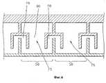
На фиг. 1 показан вид в поперечном разрезе матрицы 10 из MxN электросмещаемых управляемых отражателей, предназначенной для использования в оптической проекционной системе, раскрытой в совместно поданной заявке на патент США N 08/278 472 "Матрица электросмещаемых управляемых отражателей". Известное устройство содержит активную матрицу 11, включающую в себя подложку 12 и матрицу из MxN транзисторов на ней; матрицу 13 из MxN электросмещаемых приводов 30, где каждый из электросмещаемых приводов 30 включает в себя пару управляемых элементов 14, 15, пару электродов смещения 16, 17 и общий сигнальный электрод 18; матрицу 19 из MxN навесок 31, где каждая из навесок 31 установлена в каждом из электросмещаемых приводов 30; матрицу 20 из MxN соединенных выводов 22, каждый из которых используется для электрического соединения каждого из сигнальных электродов 18 с активной матрицей 11, и матрицу 21 из MxN отражателей 23, каждый из которых размещен на каждой из MxN подвесок 31. In FIG. 1 is a cross-sectional view of a matrix 10 of MxN electrically movable guided reflectors intended for use in an optical projection system disclosed in co-filed US Patent Application No. 08/278 472 "Matrix of Electrically Shifted Guided Reflectors". The known device contains an active matrix 11, including a substrate 12 and a matrix of MxN transistors on it; a matrix 13 of MxN electrically movable drives 30, where each of the electrically movable drives 30 includes a pair of controllable elements 14, 15, a pair of bias electrodes 16, 17, and a common signal electrode 18; a matrix 19 of MxN linkages 31, where each of the linkages 31 is installed in each of the electrically movable drives 30; a matrix 20 of MxN connected terminals 22, each of which is used to electrically connect each of the signal electrodes 18 with an active matrix 11, and a matrix 21 of MxN reflectors 23, each of which is placed on each of the MxN suspensions 31.
Имеется ряд проблем, связанных с вышеописанной матрицей электросмещаемых управляемых отражателей. Прежде всего, поскольку электросмещаемый материал, состоящий из управляющих элементов, используется в объемной форме, он, по всей вероятности, ухудшается после продолжительного использования, что, в свою очередь, влияет на характеристики управляемых отражателей в матрице. Кроме того, поскольку каждый из управляемых отражателей не отделен электрически или физически друг от друга, на действие каждого управляемого отражателя оказывают влияние соседние управляемые отражатели. There are a number of problems associated with the above matrix of electrically movable guided reflectors. First of all, since the electrically displaced material, consisting of control elements, is used in bulk, it is likely to deteriorate after prolonged use, which, in turn, affects the characteristics of controlled reflectors in the matrix. In addition, since each of the controlled reflectors is not electrically or physically separated from each other, the adjacent controlled reflectors influence the action of each controlled reflector.
В вышеупомянутой совместно поданной заявке раскрыт также способ изготовления такой матрицы из MxN электросмещаемых управляемых отражателей, в которой используется керамическая пластинка, имеющая толщину 30-50 мкм. The aforementioned co-filed application also discloses a method for manufacturing such a matrix of MxN electrically-driven guided reflectors, in which a ceramic plate having a thickness of 30-50 μm is used.
Однако имеется необходимость дальнейших усовершенствований вышеописанного способа изготовления матрицы из MxN электросмещаемых приводов. Прежде всего, довольно трудно получить керамическую пластинку, имеющую толщину 30-50 мкм; и, кроме того, при уменьшении толщины керамической пластинки до диапазона 30-50 мкм, вероятно, ухудшатся механические свойства, что, в свою очередь, затруднит процесс изготовления. However, there is a need for further improvements to the above-described method of manufacturing a matrix of MxN electrically movable drives. First of all, it is rather difficult to obtain a ceramic plate having a thickness of 30-50 microns; and, in addition, when the thickness of the ceramic plate is reduced to a range of 30-50 microns, the mechanical properties are likely to deteriorate, which, in turn, will complicate the manufacturing process.
Кроме того, это связано с затратами определенного количества времени, трудностями управления и трудоемкими процессами, в результате чего трудно обеспечить необходимую воспроизводимость, надежность и производительность, а также оказываются ограниченными возможности дальнейшего уменьшения размеров изготавливаемых изделий. In addition, this is associated with the cost of a certain amount of time, management difficulties and labor-intensive processes, as a result of which it is difficult to provide the necessary reproducibility, reliability and performance, and the possibilities for further reduction in the size of manufactured products are limited.
Поэтому задачей настоящего изобретения является создание способа изготовления матрицы из MxN управляемых отражателей, не требующего использования тонкой электросмещаемой керамической пластинки. Therefore, an object of the present invention is to provide a method for manufacturing a matrix of MxN controllable reflectors that does not require the use of a thin electrically displaceable ceramic plate.
Кроме того, задачей настоящего изобретения является создание усовершенствованного нового способа изготовления матрицы из MxN управляемых отражателей, обеспечивающего более высокую воспроизводимость, надежность и производительность. In addition, the present invention is the creation of an improved new method of manufacturing a matrix of MxN controlled reflectors, providing higher reproducibility, reliability and performance.
Еще одной задачей настоящего изобретения является создание матрицы из MxN управляемых отражателей, имеющей новую структуру, способную сохранять свои рабочие характеристики после длительного использования и имеющую улучшенный оптический коэффициент полезного действия (КПД). Another objective of the present invention is the creation of a matrix of MxN controlled reflectors having a new structure, able to maintain its performance after prolonged use and having improved optical efficiency (EFFICIENCY).
В соответствии с одним аспектом настоящего изобретения матрица из MxN тонкопленочных управляемых отражателей, предназначенная для использования в оптической проекционной системе, содержит активную матрицу, включающую в себя подложку, матрицу из MxN транзисторов и матрицу из MxN соединительных выводов, матрицу из MxN тонкопленочных управляемых структур, при этом каждая из управляющих структур включает в себя первую и вторую управляющие части идентичной структуры, каждая из первой и второй управляющих частей имеет верхнюю и нижнюю поверхности, ближний и дальний концы, каждая из первой и второй управляющих частей имеет по меньшей мере тонкопленочный слой вызывающего перемещение материала, имеющий верхнюю и нижнюю поверхности и первый, и второй электроды, причем первый электрод расположен на верхней поверхности вызывающего перемещение тонкопленочного слоя, а второй электрод - на нижней поверхности вызывающего перемещение тонкопленочного слоя, при этом электрический сигнал, прикладываемый к вызывающему перемещение тонкопленочному слою между первым и вторым электродами каждой управляющей части, вызывает деформирование вызывающего перемещение тонкопленочного слоя и, следовательно, управляющей части; матрицу из MxN поддерживающих элементов, каждый из которых имеет верхнюю и нижнюю поверхности и используется для поддержания каждой из управляющих структур на месте, а также для электрического соединения каждой из управляющих структур с активной матрицей, и матрицу из MxN отражательных слоев, каждый из которых включает в себя зеркало для отражения световых лучей, и поддерживающий слой, каждый из отражательных слоев, кроме того, имеет первую сторону, вторую противолежащую сторону и центральный расположенный между ними участок, причем первая сторона и вторая противолежащая стороны каждого из отражательных слоев прикреплены на верху первой и второй управляющих частей каждой из управляющих структур соответственно так, что, когда первая и вторая управляющие части каждой из управляющих структур деформируются под действием электрического сигнала, центральный участок соответствующего отражательного слоя наклоняется, оставаясь плоским, позволяя тем самым всему центральному участку отражать световые лучи и обеспечивая повышение оптического КПД. In accordance with one aspect of the present invention, an array of MxN thin film guided reflectors for use in an optical projection system comprises an active matrix including a substrate, an array of MxN transistors and an array of MxN terminals, an array of MxN thin film guides, for this, each of the control structures includes the first and second control parts of an identical structure, each of the first and second control parts has an upper and lower surface and, the proximal and distal ends, each of the first and second control parts has at least a thin film layer of a material causing movement, having upper and lower surfaces and a first and second electrodes, the first electrode being located on the upper surface of the movement causing thin film layer, and the second electrode - on the lower surface of the movement-causing thin-film layer, while an electrical signal applied to the movement-causing thin-film layer between the first and second electrodes Doya of the control part, causes the deformation causing the movement of the thin film layer and, therefore, the control part; a matrix of MxN supporting elements, each of which has an upper and lower surface and is used to maintain each of the control structures in place, as well as for electrically connecting each of the control structures with an active matrix, and a matrix of MxN reflective layers, each of which includes a mirror for reflecting light rays, and a supporting layer, each of the reflective layers, in addition, has a first side, a second opposite side and a central portion located between them, the first the side and the second opposite side of each of the reflection layers are attached to the top of the first and second control parts of each of the control structures, respectively, so that when the first and second control parts of each of the control structures are deformed by an electric signal, the central portion of the corresponding reflective layer is tilted, remaining flat, thereby allowing the entire central area to reflect light rays and providing increased optical efficiency.
В соответствии с другим аспектом настоящего изобретения предложен новый способ изготовления матрицы из MxN управляемых отражателей, предназначенной для использования в оптической проекционной системе, в которой используются известные тонкопленочные технологии, причем способ включает в себя этапы: обеспечения активной матрицы, имеющей верхнюю и нижнюю поверхности и включающей в себя подложку, матрицу из MxN транзисторов и матрицу из MxN соединительных выводов; формирования первого поддерживающего слоя на верхней поверхности активной матрицы, включающего в себя матрицу из MxN оснований, соответственно матрице из MxN поддерживающих элементов в матрице из MxN тонкопленочных управляемых отражателей и первую жертвенную область; обработки первой жертвенной области первого поддерживающего слоя для обеспечения возможности ее удаления; нанесения первого тонкопленочного электродного слоя на первый поддерживающий слой; формирования тонкопленочного вызывающего перемещение слоя на первом тонкопленочном электродном слое; формирования второго тонкопленочного электродного слоя на тонкопленочном вызывающем перемещение слое; формирования рисунка (структурирования) первого тонкопленочного электродного слоя, тонкопленочного вызывающего перемещение слоя и второго тонкопленочного электродного слоя в виде матрицы MxN управляемых структур и окружающих их пустых областей, причем каждая из управляющих структур включает в себя первую и вторую управляющие части; формирования второго жертвенного слоя на пустой области, окружающей каждую из управляющих структур; обработки второго жертвенного слоя, который должен быть удален; формирования рисунка (структурирование) второго жертвенного слоя в виде матрицы из MxN жертвенных элементов; нанесения второго поддерживающего слоя на матрицу из MxN управляющих структур и второй жертвенный слой, структурированный на предыдущем этапе; нанесения отражающего свет слоя на второй поддерживающий слой; формирования рисунка отражающего свет слоя и второго поддерживающего слоя в виде матрицы из MxN отражательных слоев; и удаления первого жертвенного слоя и матрицы из MxN жертвенных элементов для формирования таким образом упомянутой матрицы из MxN тонкопленочных управляемых отражателей. In accordance with another aspect of the present invention, there is provided a new method for manufacturing an MxN array of guided reflectors for use in an optical projection system using known thin film technologies, the method comprising the steps of: providing an active matrix having upper and lower surfaces and including a substrate, an array of MxN transistors, and an array of MxN connectors; the formation of the first supporting layer on the upper surface of the active matrix, which includes a matrix of MxN bases, respectively, a matrix of MxN supporting elements in a matrix of MxN thin-film controlled reflectors and the first sacrificial region; processing the first sacrificial region of the first support layer to enable its removal; applying the first thin film electrode layer to the first supporting layer; forming a thin film layer causing the displacement on the first thin film electrode layer; forming a second thin film electrode layer on the thin film displacement causing layer; forming a pattern (structuring) of the first thin-film electrode layer, a thin-film moving layer and a second thin-film electrode layer in the form of a matrix MxN of controlled structures and surrounding empty areas, each of the control structures including the first and second control parts; forming a second sacrificial layer on an empty area surrounding each of the control structures; processing a second sacrificial layer to be removed; forming a pattern (structuring) of the second sacrificial layer in the form of a matrix of MxN sacrificial elements; applying a second support layer to the matrix of MxN control structures and a second sacrificial layer structured in the previous step; applying a light reflecting layer to the second support layer; forming a pattern of a light reflecting layer and a second supporting layer in the form of a matrix of MxN reflective layers; and removing the first sacrificial layer and matrix from MxN sacrificial elements to form the matrix of MxN thin film guided reflectors thus formed.
Вышеприведенные и другие цели и особенности настоящего изобретения станут очевидными из последующего описания предпочтительных вариантов его осуществления, иллюстрируемого чертежами, на которых представлено следующее:
фиг. 1 - вид в поперечном разрезе известной конструкции матрицы из MxN электросмещаемых управляемых отражателей;
фиг. 2 - вид в поперечном разрезе MxN тонкопленочных управляемых отражателей в соответствии с первым предпочтительным вариантом осуществления настоящего изобретения;
фиг. 3 - детальный вид в поперечном разрезе первого варианта осуществления матрицы тонкопленочных управляемых отражателей по фиг. 2;
фиг. 4 - вид сверху первого варианта осуществления матрицы тонкопленочных управляемых отражателей по фиг. 2;
фиг. 5 - детальное пространственное представление первого варианта осуществления тонкопленочных управляемых отражателей по фиг. 2;
фиг. 6 - другая возможная конфигурация отражательного слоя для первого варианта осуществления изобретения;
фиг. 7 - вид в поперечном разрезе тонкопленочного управляемого отражателя согласно первому варианту осуществления изобретения в возбужденном состоянии;
фиг. 8 - вид в поперечном разрезе тонкопленочного управляемого отражателя биморфной структуры согласно второму варианту осуществления изобретения;
фиг. 9 - вид в поперечном разрезе матрицы из MxN тонкопленочных управляемых отражателей, соответствующей третьему предпочтительному варианту осуществления настоящего изобретения;
фиг. 10 - детальный вид в поперечном разрезе соответствующей третьему варианту осуществления матрицы тонкопленочных управляемых отражателей по фиг. 9;
фиг. 11 - пространственное представление соответствующей третьему варианту осуществления матрицы тонкопленочных управляемых отражателей по фиг. 9;
фиг. 12A - 12J - схематичное представление в поперечном разрезе, иллюстрирующее этап изготовления конструкции согласно первому варианту осуществления изобретения.The above and other objectives and features of the present invention will become apparent from the following description of the preferred options for its implementation, illustrated by the drawings, which represent the following:
FIG. 1 is a cross-sectional view of a known matrix design of MxN electrically displaceable guided reflectors;
FIG. 2 is a cross-sectional view MxN of thin film guided reflectors in accordance with a first preferred embodiment of the present invention;
FIG. 3 is a detailed cross-sectional view of a first embodiment of a matrix of thin-film guided reflectors of FIG. 2;
FIG. 4 is a plan view of a first embodiment of a matrix of thin film guided reflectors of FIG. 2;
FIG. 5 is a detailed spatial representation of a first embodiment of the thin film guided reflectors of FIG. 2;
FIG. 6 is another possible reflection layer configuration for a first embodiment of the invention;
FIG. 7 is a cross-sectional view of a thin film controllable reflector according to a first embodiment of the invention in an excited state;
FIG. 8 is a cross-sectional view of a thin film controlled reflector of a bimorph structure according to a second embodiment of the invention;
FIG. 9 is a cross-sectional view of an MxN array of thin film guided reflectors according to a third preferred embodiment of the present invention;
FIG. 10 is a detailed cross-sectional view of a third embodiment of a matrix of thin film guided reflectors of FIG. nine;
FIG. 11 is a spatial representation of a matrix of thin film guided reflectors of FIG. nine;
FIG. 12A to 12J are a schematic cross-sectional view illustrating a manufacturing step of a structure according to a first embodiment of the invention.
На фиг. 2 - 12 схематично представлены виды в поперечном разрезе заявленной матрицы из MxN тонкопленочных управляемых отражателей, где M и N - целые числа, предназначенной для использования в оптической проекционной системе, и иллюстрации способа ее изготовления, соответствующие предпочтительным вариантам осуществления настоящего изобретения. Следует отметить, что одинаковые элементы на фиг. 2 - 12 обозначены одинаковыми позициями. In FIG. 2 to 12 are schematic cross-sectional views of the claimed matrix of MxN thin-film controlled reflectors, where M and N are integers intended for use in an optical projection system, and an illustration of a method for manufacturing it according to preferred embodiments of the present invention. It should be noted that the same elements in FIG. 2 to 12 are denoted by the same reference numerals.
На фиг. 2 представлен вид в поперечном разрезе первого варианта матрицы 50 из MxN тонкопленочных управляемых отражателей 51, содержащей активную матрицу 52, матрицу 53 из MxN тонкопленочных управляющих структур 54, матрицу 55 из MxN поддерживающих элементов 56 и матрицу 57 из MxN отражательных слоев 58. In FIG. 2 is a cross-sectional view of a first embodiment of a
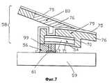
На фиг. 3 представлен детальный вид в поперечном разрезе показанной на фиг. 2 матрицы 50 тонкопленочных управляемых отражателей. Активная матрица 52 включает в себя подложку 59, матрицу из MxN транзисторов (не показаны) и матрицу из MxN соединительных выводов 61. Каждая из управляющих структур 54 включает в себя идентичные первую и вторую управляющие части 62(a), 62(b), причем каждая управляющая часть, например 62(a), имеет верхнюю и нижнюю поверхности 63, 64, ближний и дальний концы 65, 66. Каждая управляющая часть, например 62(b), дополнительно имеет по меньшей мере тонкопленочный слой 67 вызывающего перемещение материала, например пьезоэлектрического материала, электрострикционного материала или магнитострикционного материала, имеющего верхнюю и нижнюю поверхности 68, 69 и первый и второй электроды 70, 71, причем первый электрод 70 расположен на верхней поверхности 68 вызывающего перемещение слоя 67, а второй электрод 71 расположен на нижней поверхности 69 вызывающего перемещение слоя 67. Если вызывающий перемещение слой 67 выполнен из пьезоэлектрического материала, например, титаната циркония-свинца, он должен быть поляризован. Первый и второй электроды выполняют из материала типа золота (Au) или серебра (Ag). In FIG. 3 is a detailed cross-sectional view of FIG. 2 arrays of 50 thin-film controlled reflectors. The
Каждый из MxN поддерживающих элементов 56, имеющий верхнюю и нижнюю поверхности 72, 73, используется для поддержания первой и второй управляющих частей 62(a), 62(b) каждой из управляющих структур 54 на месте; а также для электрического соединения второго электрода 71 в первой и второй управляющих частях 62(a), 62(b) в каждой из управляющих структур 54 с соответствующим соединительным выводом 61 на активной матрице 52 посредством обеспечения перемычки 99 из электрически проводящего материала, например металла. В этой соответствующей изобретению матрице 50 из MxN тонкопленочных управляемых отражателей 51, каждая из первой и второй управляющих частей 62(a), 62(b) в каждой из управляющих структур 54 заделана одним концом в соответствующем элементе 56 посредством закрепления на верхней поверхности 72 каждого из поддерживающих элементов 56 на нижней поверхности 64 каждой из первой и второй управляющих частей 62(a), 62(b) в каждой из управляющих структур 54 на ближнем ее конце 65, а нижняя поверхность 73 каждого из поддерживающих элементов 56 расположена на верху активной матрицы 52. Each of the
Каждый отражательный слой 58, включающий отражатель 75, предназначенный для отражения световых лучей, и поддерживающий слой 76, имеющий верхнюю поверхность 77, имеет первую сторону 78, вторую противолежащую сторону 79 и расположенный между ними центральный участок 80, как показано на фиг. 4. Первая сторона 78 и вторая противолежащая сторона 79 каждого из отражательных слоев 58 расположены на верху первой и второй управляющих частей 62(a), 62(b) каждой из управляющих структур 54 соответственно. Each
Когда электрическое поле прикладывается к вызывающему перемещение слою 67 между первым и вторым электродами 70, 71 каждой из управляющих частей 62(a), 62(b) в каждой из управляющих структур 54, вызывающий перемещение слой 67 деформируется, что, в свою очередь, вызывает деформирование первой стороны 78 и второй противолежащей стороны соответствующего отражательного слоя 58. При такой ситуации центральный участок 80 соответствующего отражательного слоя 58 в отличие от первой стороны 78 и второй противолежащей стороны 79 не деформируется, то есть остается плоским, обеспечивая увеличение оптического КПД. When an electric field is applied to the displacement-causing
На фиг. 5 и 6 показано пространственное представление тонкопленочного управляемого отражателя 51 согласно первому варианту осуществления и второй возможной конфигурации отражательного слоя для матрицы 50 из MxN тонкослойных управляемых отражателей 51 соответственно. In FIG. 5 and 6 show a spatial representation of a thin-film controlled
Материал, из которого изготавливают поддерживающий слой 76 в каждом из отражательных слоев 58, может быть также светоотражающим, например алюминием (Al), что позволяет использовать его верхнюю поверхность 77 в качестве отражателя 75 в каждом из тонкопленочных управляемых отражателей 51. The material from which the
В случае предложенной матрицы 50 тонкопленочных управляемых отражателей 51 она может функционировать в равной степени хорошо благодаря наличию верхней и нижней поверхностей 68, 69 вызывающего перемещение тонкопленочного слоя 67 в каждой из управляющих структур 54, полностью покрытых первым и вторым электродами 70, 71, или благодаря наличию одной из поверхностей 68, 69 вызывающего перемещение тонкопленочного слоя 67 в каждой из управляющих структур 54, покрытой частично первым и вторым электродами 70, 71. In the case of the proposed
В качестве примера первого варианта осуществления изобретения на фиг. 3 и 7 показана матрица 50 из MxN тонкопленочных управляемых отражателей 51, содержащая матрицу 53 из MxN управляющих структур 54, выполненных из пьезоэлектрического материала, например, свинцового титаната циркония-свинца. Электрическое поле прикладывают к пьезоэлектрическому тонкопленочному слою 67, расположенному между первым и вторым электродами 70, 71 в каждой из управляющих частей 62(a), 62(b) в каждой из управляющих структур 54. Положение электрического поля заставляет пьезоэлектрический материал либо сжиматься, либо растягиваться в зависимости от полярности электрического поля относительно поляризации пьезоэлекрического материала. Если полярность электрического поля соответствует полярности пьезоэлектрического материала, пьезоэлектрический материал сжимается. Если полярность электрического поля противоположна полярности пьезоэлектрического материала, пьезоэлектрический материал растягивается. As an example of a first embodiment of the invention in FIG. 3 and 7, an
На фиг. 7 полярность пьезоэлектрического материала соответствует полярности приложенного электрического поля, вызывая сжатие пьезоэлектрического материала. В таком случае первая и вторая управляющие части 62(a), 62(b) каждой из управляющих структур 54 изогнуты вниз, как показано на фиг. 7, наклоняя тем самым первую сторону 78 и вторую противолежащую сторону 79 отражательного слоя 58 вниз на определенный угол. Однако центральный участок 80 отражательного слоя 58 остается плоским, и в результате этого эффективная длина отражательного слоя 58 представляет собой полную длину центрального участка 80 отражательного слоя 58. В противоположность этому, если отражательный слой 58 непосредственно прикрепить к управляющей структуре 54, участок отражательного слоя 58, прикрепленный к поддерживающему элементу 56, не деформируется под действием электрического поля, а сохраняет свое положение. В результате этого эффективная длина отражательного слоя 58 оказывается меньше длины участка управляющей структуры 54, прикрепленной к поддерживающему элементу 56. Поэтому выполнение первой стороны 78, второй противолежащей стороны 79 и прикрепленных к ним первой и второй управляющих частей 62(a), 62(b) соответственно в первом, показанном на фиг. 3, варианте увеличивает коэффициент заполнения и эффективность матрицы 57 отражательных слоев 58. Как следует из фиг. 3 и 7, свет, падающий на отражательный слой 58 показанного на фиг. 7 управляемого отражателя 52, отклоняется на больший угол, чем свет, отраженный от незадействованного управляемого отражателя 51, показанного на фиг. 3. Как вариант, к вызывающему перемещение тонкопленочному пьезоэлектрическому слою 67 можно приложить электрическое поле обратной полярности, вызывающее растяжение пьезоэлектрического материала. В этом случае управляющая структура 54 изгибается вверх (не показано). Свет, падающий на отражательный слой 58 изогнутого вверх управляемого отражателя 51, отклоняется под меньшим углом, чем свет, отклоненный от незадействованного управляемого отражателя 51, показанного на фиг. 3. In FIG. 7, the polarity of the piezoelectric material corresponds to the polarity of the applied electric field, causing compression of the piezoelectric material. In this case, the first and second control parts 62 (a), 62 (b) of each of the
На фиг. 8 представлен вид в поперечном разрезе второго варианта осуществления матрицы 100 из MxN тонкопленочных управляемых отражателей 101, причем второй вариант осуществления аналогичен первому варианту, за исключением того, что каждая из первой и второй управляющих частей 62(a), 62(b) в каждой из управляющих структур 54 представляет собой биморфную структуру, включающую первый электрод 70, второй электрод 71, промежуточный металлический слой 87, верхний вызывающий перемещение тонкопленочный слой 89, имеющий верхнюю и нижнюю поверхности 90, 91, и нижний вызывающий перемещение тонкопленочный слой 92, имеющий верхнюю и нижнюю поверхности 93, 94. В каждой из управляющих частей 62(a), 62(b) верхний и нижний вызывающие перемещение тонкопленочные слои 89, 92 разделены промежуточным металлическим слоем 87, причем первый электрод 70 расположен на верхней поверхности 90 верхнего вызывающего перемещения тонкопленочного слоя 89, а второй электрод 71 расположен на нижней поверхности 94 нижнего вызывающего перемещение тонкопленочного слоя 92. In FIG. 8 is a cross-sectional view of a second embodiment of a
Как и в случае первого варианта, верхний и нижний вызывающие перемещение тонкопленочные слои 89, 92 в каждой из управляющих структур 54 выполнены из пьезоэлектрического материала, электрострикционной керамики или магнитострикционной керамики. В случае, когда верхний и нижний вызывающие перемещение тонкопленочные слои 89, 92 изготавливают из пьезоэлектрического материала, например, из пьезоэлектрической керамики или пьезоэлектрического полимера, верхний и нижний вызывающие перемещение тонкопленочные слои 89, 92 должны быть поляризованы таким образом, чтобы направление поляризации пьезоэлектрического материала в верхнем вызывающем перемещение тонкопленочном слое 89 было противоположным направлению поляризации в нижнем вызывающем перемещение тонкопленочном слое 92. As in the case of the first embodiment, the upper and lower displacement-causing thin film layers 89, 92 in each of the
В качестве примера функционирования второго варианта осуществления изобретения предположим, что верхний и нижний вызывающие перемещение слои 89, 92 в матрице 100 из MxN тонкопленочных управляемых отражателей 101, показанных на фиг. 8, изготовлены из пьезоэлектрического материала, например, из титаната циркония свинца (ТЦС). При приложении к каждой из управляющих структур 54 электрического поля верхний и нижний вызывающие перемещение тонкопленочные пьезоэлектрические слои 89, 92 управляющих структур 54 изгибаются вверх или вниз в зависимости от поляризации пьезоэлектрического материала и полярности электрического поля. Например, если полярность верхнего вызывающего перемещение тонкопленочного пьезоэлектрического слоя 89 заставляет его сжиматься, а нижний вызывающий перемещение тонкопленочный пьезоэлектрический слой 92 растягивается, то управляющие части 62(a), 62(b) в каждой из управляющих структур 54 изгибаются вверх. В этой ситуации падающий свет отклоняется от управляемого отражателя 51 под меньшим углом, чем отклоняемый свет от незадействованного управляемого отражателя 51. Однако, если полярность пьезоэлектрического материала и электрического поля заставляет верхний вызывающий перемещение тонкопленочный пьезоэлектрический слой 89 растягиваться, а нижний вызывающий перемещение тонкопленочный пьезоэлектрический слой 92 сжиматься, то управляющая структура 54 изгибается вниз. В этой ситуации падающий свет отклоняется под большим углом от управляемого отражателя 51, чем в случае отклонения света от незадействованного управляемого отражателя. As an example of the functioning of the second embodiment, suppose that the upper and lower displacement-causing
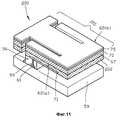
На фиг. 9 схематично показан вид в поперечном разрезе третьего варианта матрицы 200 из MxN тонкопленочных управляемых отражателей 201. Третий вариант аналогичен первому варианту, за исключением того, что в первой и второй управляющих частях 62(a), 62(b) каждой управляющей структуры 54 отсутствует поддерживающий слой 76 в отражательном слое 58. Вместо этого они снабжены эластичным слоем 202, расположенным на нижней поверхности 69 вызывающего перемещения слоя 67, как показано на фиг. 10. Обычно, когда эластичный слой предусматривается в управляемом отражателе, то вызывающий перемещение и эластичный слои, как правило, разделяют слоем дорогостоящего электрически проводящего металла, например платины (Pt), для улучшения адгезии между ними. In FIG. 9 is a schematic cross-sectional view of a third embodiment of an
Однако, если коэффициент теплового расширения материалов, образующих эластичный слой и вызывающий перемещение слой, сильно отличаются друг от друга, а контакт между эластичным слоем и электрически проводящим металлическим слоем или контакт между вызывающим перемещение слоем и электрически проводящим слоем слабый, то это может привести к отслаиванию электрически проводящего металлического слоя, снижая тем самым рабочие характеристики управляемого отражателя. Эту проблему можно решить за счет выполнения эластичного и вызывающего перемещение слоев из материалов, имеющих одинаковую структуру, например, перовскита. Поскольку материалы, составляющие эластичный и вызывающий перемещение слои, имеют аналогичную структуру, улучшается адгезия между ними, устраняя тем самым необходимость использования электрически проводящего металлического слоя, а также обеспечивая возможность легче управлять потенциальной энергией деформации между ними. Одним из возможных сочетаний таких материалов является ТЦС для вызывающего перемещение слоя и титанат свинца (PbTiO3) для эластичного слоя. В этом случае материал эластичного слоя отличается высокой диэлектрической проницаемостью (ε) и низкой пьезоэлектрической постоянной (d).However, if the coefficient of thermal expansion of the materials forming the elastic layer and the displacement-causing layer is very different from each other, and the contact between the elastic layer and the electrically conductive metal layer or the contact between the displacement-causing layer and the electrically conductive layer is weak, this can lead to peeling an electrically conductive metal layer, thereby reducing the performance of a controlled reflector. This problem can be solved by performing elastic and moving layers of materials having the same structure, for example, perovskite. Since the materials that make up the elastic and displacement layers have a similar structure, the adhesion between them improves, eliminating the need to use an electrically conductive metal layer, and also making it easier to control the potential strain energy between them. One possible combination of such materials is SCC for the displacement layer and lead titanate (PbTiO3 ) for the elastic layer. In this case, the material of the elastic layer is characterized by a high dielectric constant (ε) and a low piezoelectric constant (d).
Кроме того, если первый электрод выполнен из светоотражающего материала, например из алюминия, то отражательный слой 58 можно исключить. В таком случае первый электрод также функционирует как отрицательный слой 58. In addition, if the first electrode is made of reflective material, such as aluminum, then the
На фиг. 12A-12J показаны этапы изготовления, используемые при изготовлении конструкции по первому варианту осуществления настоящего изобретения. Процесс изготовления первого варианта, то есть матрицы 50 из MxN тонкопленочных управляемых отражателей 51, где M и N - целые числа, начинается с приготовления активной матрицы 52, имеющей верхнюю и нижнюю поверхности 102, 103, включающей подложку 59, матрицу из MxN транзисторов (не показаны) и матрицу из MxN соединительных выводов 61, как показано на фиг. 12A. In FIG. 12A-12J illustrate manufacturing steps used in manufacturing the structure of the first embodiment of the present invention. The manufacturing process of the first embodiment, that is, the
На следующем этапе на верхней поверхности 102 активной матрицы 52 образуют первый поддерживающий слой 106, включающий в себя матрицу из MxN оснований 108, соответствующих матрице 55 из MxN поддерживающих элементов 56, и первую жертвенную область 109, при этом первый поддерживающий слой 106 образуют посредством нанесения первого жертвенного слоя (не показано) на всю верхнюю поверхность 102 активной матрицы 52; образования матрицы из MxN пустых прорезей (не показаны) для образования тем самым первой жертвенной области 109, где каждая из пустых прорезей расположена вокруг каждого из MxN соединительных выводов 61; и формирования основания 108 в каждой из пустых прорезей, как показано на фиг. 12B. Первый жертвенный слой образуют способом напыления, матрицу пустых прорезей - способом травления, а оснований - способом напыления или химического осаждения из паровой фазы, с последующим травлением. Затем жертвенную область 109 первого поддерживающего слоя 106 обрабатывают таким образом, чтобы ее можно было позже удалить с использованием травления или применением химических реактивов. In the next step, on the
В каждом из оснований 108 образуют перемычку 99, предназначенную для электрического соединения каждого из соединительных выводов 61 с каждым из верхних электродов 71, выполненную из электрически проводящего материала, например, вольфрама (W), посредством создания вначале отверстия, проходящего от верха основания к верхней части соответствующего соединительного вывода 61, с использованием метода травления, а затем заполнения его электрически проводящим материалом, как показано на фиг. 12C. In each of the
На следующем этапе, как показано на фиг. 12D, на первый поддерживающий слой 106 наносят первый тонкопленочный электродный слой 111 из электрически проводящего материала, например из золота (Au). После этого на первом тонкопленочном электродном слое 111 формируют вызывающий перемещение слой 112 из вызывающего перемещение материала, например ТЦС, и второй тонкопленочный электродный слой 113. In the next step, as shown in FIG. 12D, a first thin
После этого в первом тонкопленочном электродном слое 111, тонкопленочном вызывающем перемещение слое 112 и втором тонкопленочном электродном слое 113 создают рисунок (структурируют указанные слои) в виде матрицы 53 из MxN управляющих структур 54 и пустой области (не показана), окружающей каждую из управляющих структур 54, причем каждая из управляющих структур 54 включает в себя первую и вторую управляющие части 62(a), 62(b), как показано на фиг. 12E. Thereafter, in the first thin
После этого на пустой области, окружающей каждую из управляющих структур 54, формируют второй жертвенный слой 114, как показано на фиг. 12F. Затем второй жертвенный слой 114 обрабатывают таким образом, чтобы его можно было впоследствии удалить. Thereafter, a second
Затем в жертвенном слое, как показано на фиг. 12G, создают рисунок в виде матрицы из MxN жертвенных элементов 116. После этого на верх матрицы 53 из MxN управляющих структур 54 и на второй жертвенный слой 116 с предварительно созданным рисунком последовательно наносят второй поддерживающий слой 117 и светоотражающий слой 119, содержащий в себе отражательный слой 58, как показано на фиг. 12H. Then, in the sacrificial layer, as shown in FIG. 12G, create a pattern in the form of a matrix of MxN
Затем в светоотражательном слое 119 и втором поддерживающем слое 117 создают рисунок в виде матрицы 57 из MxN отражательных слоев 58, как показано на фиг. 121. Then, a pattern in the form of a
Тонкопленочные слои электрически проводящего, вызывающего перемещение и отражающего свет материалов можно наносить и создавать в них рисунок известными тонкопленочными методами, например, напылением, золь-гелевым способом, выпариванием, травлением и микромеханической обработкой. Thin film layers of electrically conductive, moving and light reflecting materials can be applied and patterned using known thin film methods, for example, by spraying, sol-gel, evaporation, etching and micromechanical processing.
После этого первую жертвенную область 109 и матрицу 115 из MxN жертвенных элементов 116 удаляют или растворяют посредством применения химических реактивов, образуя, таким образом, упомянутую матрицу 50 из MxN тонкопленочных управляемых отражателей 51, как показано на фиг. 12J. Thereafter, the first
Изготовление второго варианта осуществляется аналогично изготовлению первого варианта за исключением того, что требуются два дополнительных этапа: формирование дополнительного вызывающего перемещение слоя и промежуточного металлического слоя. The manufacture of the second embodiment is carried out similarly to the manufacture of the first embodiment, except that two additional steps are required: the formation of an additional layer causing a displacement and an intermediate metal layer.
В случае третьего варианта осуществления изобретения, поскольку каждую из первой и второй управляющих частей 62(a), 62(b) в каждой из управляющих структур 54 снабжают эластичным слоем 202 на нижней поверхности вызывающего перемещение слоя 67, исключая поддерживающий слой 76, этапы изготовления третьего варианта осуществления изобретения по существу такие же, как и этапы изготовления первого варианта, с несколько измененной последовательностью. Кроме того, если второй эластичный слой изготавливают из отражающего свет материала, например алюминия, то этап, включающий формирование отражающего свет слоя 119, можно также исключить из общей процедуры изготовления. In the case of the third embodiment, since each of the first and second control parts 62 (a), 62 (b) in each of the
Хотя настоящее изобретение описано только относительно определенных предпочтительных вариантов его осуществления, могут быть осуществлены другие модификации и видоизменения изобретения без изменения объема настоящего изобретения, определяемого формулой изобретения. Although the present invention has been described only with respect to certain preferred embodiments, other modifications and variations of the invention may be made without altering the scope of the present invention as defined by the claims.
Claims (38)
Translated fromRussianПриоритет 16.11.93. по пп.1 - 27, 33 - 38;
Приоритет 30.12.93. по пп.28 - 32.priority on points:
Priority 11.16.93. according to claims 1 - 27, 33 - 38;
Priority 12/30/93. PP.28 - 32.
Applications Claiming Priority (6)
| Application Number | Priority Date | Filing Date | Title |
|---|---|---|---|
| KR93-24397 | 1993-11-16 | ||
| KR1019930024397AKR970006693B1 (en) | 1993-11-16 | 1993-11-16 | An optical path regulating apparatus of projection type of image display |
| KR93024395AKR970006691B1 (en) | 1993-11-16 | 1993-11-16 | A manufacturing method of an optical path regulating apparatus |
| KR93-24395 | 1993-11-16 | ||
| KR93-31716 | 1993-12-30 | ||
| KR1019930031716AKR970008400B1 (en) | 1993-12-30 | 1993-12-30 | Structure of Light Path Adjusting Device of Projection-type Image Display Device and Manufacturing Method Thereof |
Publications (2)
| Publication Number | Publication Date |
|---|---|
| RU96113083A RU96113083A (en) | 1998-09-27 |
| RU2125347C1true RU2125347C1 (en) | 1999-01-20 |
Family
ID=27349019
Family Applications (1)
| Application Number | Title | Priority Date | Filing Date |
|---|---|---|---|
| RU96113083ARU2125347C1 (en) | 1993-11-16 | 1994-11-15 | Array of thin-film controlled reflectors for optical projection system and its manufacturing process |
Country Status (16)
| Country | Link |
|---|---|
| US (3) | US5835293A (en) |
| EP (1) | EP0653657B1 (en) |
| JP (1) | JP3253304B2 (en) |
| CN (1) | CN1047904C (en) |
| AU (1) | AU693139B2 (en) |
| BR (1) | BR9408054A (en) |
| CA (1) | CA2176347A1 (en) |
| CZ (1) | CZ287202B6 (en) |
| DE (1) | DE69423070T2 (en) |
| ES (1) | ES2145086T3 (en) |
| HU (1) | HU220515B1 (en) |
| IT (1) | IT1271062B (en) |
| PL (1) | PL175809B1 (en) |
| RU (1) | RU2125347C1 (en) |
| TW (1) | TW266328B (en) |
| WO (1) | WO1995014351A1 (en) |
Cited By (1)
| Publication number | Priority date | Publication date | Assignee | Title |
|---|---|---|---|---|
| RU2401448C1 (en)* | 2008-08-26 | 2010-10-10 | Эйсер Инкорпорейтед | Complex pixel element, complex touch-sensitive liquid-crystal panel and method of controlling said panel |
Families Citing this family (24)
| Publication number | Priority date | Publication date | Assignee | Title |
|---|---|---|---|---|
| JP3471156B2 (en)* | 1995-05-30 | 2003-11-25 | シャープ株式会社 | Image shift mechanism and imaging device |
| US6969635B2 (en)* | 2000-12-07 | 2005-11-29 | Reflectivity, Inc. | Methods for depositing, releasing and packaging micro-electromechanical devices on wafer substrates |
| US6849471B2 (en)* | 2003-03-28 | 2005-02-01 | Reflectivity, Inc. | Barrier layers for microelectromechanical systems |
| KR980003662A (en)* | 1996-06-28 | 1998-03-30 | 배순훈 | Thin film type optical path adjusting device having a large driving angle |
| JPH11514105A (en)* | 1996-08-13 | 1999-11-30 | テーウー エレクトロニクス カンパニー リミテッド | Thin-film optical path adjusting device and method of manufacturing the same |
| US5949568A (en)* | 1996-12-30 | 1999-09-07 | Daewoo Electronics Co., Ltd. | Array of thin film actuated mirrors having a levelling member |
| WO1998033327A1 (en)* | 1997-01-23 | 1998-07-30 | Daewoo Electronics Co., Ltd. | Thin film actuated mirror array in an optical projection system and method for manufacturing the same |
| CA2278624A1 (en)* | 1997-01-23 | 1998-07-30 | Daewoo Electronics Co., Ltd. | Thin film actuated mirror array in an optical projection system and method for manufacturing the same |
| RU2180158C2 (en)* | 1997-01-23 | 2002-02-27 | Дэу Электроникс Ко., Лтд. | Thin-film matrix of controlled mirrors for optical projection system and its manufacturing process |
| KR19980069199A (en)* | 1997-02-27 | 1998-10-26 | 배순훈 | Thin film type optical path adjusting device and its manufacturing method which can improve the light efficiency |
| WO1999023832A1 (en)* | 1997-10-31 | 1999-05-14 | Daewoo Electronics Co., Ltd. | Method for manufacturing thin film actuated mirror array in an optical projection system |
| US20010040675A1 (en)* | 2000-01-28 | 2001-11-15 | True Randall J. | Method for forming a micromechanical device |
| KR20030060622A (en)* | 2002-01-10 | 2003-07-16 | 주식회사 대우일렉트로닉스 | Method for manufacturing thin-film micromirror array-actuated |
| US6965468B2 (en) | 2003-07-03 | 2005-11-15 | Reflectivity, Inc | Micromirror array having reduced gap between adjacent micromirrors of the micromirror array |
| US7391723B2 (en)* | 2002-04-22 | 2008-06-24 | Computer Network Technology Corporation | Frame-level fibre channel CRC on switching platform |
| US7281808B2 (en)* | 2003-06-21 | 2007-10-16 | Qortek, Inc. | Thin, nearly wireless adaptive optical device |
| US6947201B2 (en) | 2003-12-08 | 2005-09-20 | Xinetics, Inc. | Transverse electrodisplacive actuator array |
| JP4552606B2 (en)* | 2004-11-10 | 2010-09-29 | パナソニック株式会社 | Piezoelectric actuator and light sweep device using the same |
| US20090122428A1 (en)* | 2007-11-09 | 2009-05-14 | Nikon Corporation | Reflective optical elements exhibiting multimetallic-like self-correction of distortions caused by heating |
| US8654434B2 (en)* | 2010-07-20 | 2014-02-18 | Oclaro (New Jersey), Inc. | WSS with pixel gap compensation |
| DE102012221831A1 (en)* | 2012-11-29 | 2014-06-05 | Carl Zeiss Smt Gmbh | Arrangement for actuating at least one optical element in an optical system |
| KR102001460B1 (en)* | 2013-03-18 | 2019-07-19 | 삼성디스플레이 주식회사 | Optical module for laser beam shaking |
| WO2016124253A1 (en) | 2015-02-06 | 2016-08-11 | Optotune Ag | Optical device for enhancing resolution of an image |
| CN114779464A (en)* | 2022-05-24 | 2022-07-22 | 北京有竹居网络技术有限公司 | Optical signal modulator, control method and projection device |
Citations (5)
| Publication number | Priority date | Publication date | Assignee | Title |
|---|---|---|---|---|
| US4639788A (en)* | 1984-12-07 | 1987-01-27 | New York Institute Of Technology | Video display method and apparatus |
| US5085497A (en)* | 1990-03-16 | 1992-02-04 | Aura Systems, Inc. | Method for fabricating mirror array for optical projection system |
| US5090795A (en)* | 1987-10-22 | 1992-02-25 | Hughes Aircraft Company | Integrated adaptive optics apparatus |
| US5126836A (en)* | 1989-11-01 | 1992-06-30 | Aura Systems, Inc. | Actuated mirror optical intensity modulation |
| RU2002286C1 (en)* | 1990-04-12 | 1993-10-30 | Хехст АГ (DE) | Process of manufacture of liquid crystal change over and indicating device stable of loads |
Family Cites Families (25)
| Publication number | Priority date | Publication date | Assignee | Title |
|---|---|---|---|---|
| US2016962A (en)* | 1932-09-27 | 1935-10-08 | Du Pont | Process for producing glucamines and related products |
| US1985424A (en)* | 1933-03-23 | 1934-12-25 | Ici Ltd | Alkylene-oxide derivatives of polyhydroxyalkyl-alkylamides |
| US2703798A (en)* | 1950-05-25 | 1955-03-08 | Commercial Solvents Corp | Detergents from nu-monoalkyl-glucamines |
| US2920529A (en)* | 1952-05-23 | 1960-01-12 | Blythe Richard | Electronic control of optical and near-optical radiation |
| US3614677A (en)* | 1966-04-29 | 1971-10-19 | Ibm | Electromechanical monolithic resonator |
| US3544201A (en)* | 1968-01-02 | 1970-12-01 | Gen Telephone & Elect | Optical beam deflector |
| US3758199A (en)* | 1971-11-22 | 1973-09-11 | Sperry Rand Corp | Piezoelectrically actuated light deflector |
| US4441791A (en)* | 1980-09-02 | 1984-04-10 | Texas Instruments Incorporated | Deformable mirror light modulator |
| US4518976A (en)* | 1982-11-17 | 1985-05-21 | Konishiroku Photo Industry Co., Ltd. | Recording apparatus |
| US4979789A (en)* | 1989-06-02 | 1990-12-25 | Aura Systems, Inc. | Continuous source scene projector |
| US5032906A (en)* | 1989-07-12 | 1991-07-16 | Aura Systems, Inc. | Intensity calibration method for scene projector |
| US5022745A (en)* | 1989-09-07 | 1991-06-11 | Massachusetts Institute Of Technology | Electrostatically deformable single crystal dielectrically coated mirror |
| US4954789A (en)* | 1989-09-28 | 1990-09-04 | Texas Instruments Incorporated | Spatial light modulator |
| US5260798A (en)* | 1989-11-01 | 1993-11-09 | Aura Systems, Inc. | Pixel intensity modulator |
| US5150205A (en)* | 1989-11-01 | 1992-09-22 | Aura Systems, Inc. | Actuated mirror optical intensity modulation |
| US5245369A (en)* | 1989-11-01 | 1993-09-14 | Aura Systems, Inc. | Scene projector |
| US5185660A (en)* | 1989-11-01 | 1993-02-09 | Aura Systems, Inc. | Actuated mirror optical intensity modulation |
| US5035475A (en)* | 1990-03-15 | 1991-07-30 | Aura Systems, Inc. | Unique modulation television |
| US5138309A (en)* | 1990-04-03 | 1992-08-11 | Aura Systems, Inc. | Electronic switch matrix for a video display system |
| US5209119A (en)* | 1990-12-12 | 1993-05-11 | Regents Of The University Of Minnesota | Microdevice for sensing a force |
| US5218512A (en)* | 1991-08-16 | 1993-06-08 | Rohm Co., Ltd. | Ferroelectric device |
| US5159225A (en)* | 1991-10-18 | 1992-10-27 | Aura Systems, Inc. | Piezoelectric actuator |
| US5247222A (en)* | 1991-11-04 | 1993-09-21 | Engle Craig D | Constrained shear mode modulator |
| JP2665106B2 (en)* | 1992-03-17 | 1997-10-22 | 日本碍子株式会社 | Piezoelectric / electrostrictive film element |
| US5481396A (en)* | 1994-02-23 | 1996-01-02 | Aura Systems, Inc. | Thin film actuated mirror array |
- 1994
- 1994-11-15CACA002176347Apatent/CA2176347A1/ennot_activeAbandoned
- 1994-11-15DEDE69423070Tpatent/DE69423070T2/ennot_activeExpired - Lifetime
- 1994-11-15CZCZ19961413Apatent/CZ287202B6/ennot_activeIP Right Cessation
- 1994-11-15WOPCT/KR1994/000164patent/WO1995014351A1/enactiveIP Right Grant
- 1994-11-15JPJP51435395Apatent/JP3253304B2/ennot_activeExpired - Lifetime
- 1994-11-15ESES94118035Tpatent/ES2145086T3/ennot_activeExpired - Lifetime
- 1994-11-15EPEP94118035Apatent/EP0653657B1/ennot_activeExpired - Lifetime
- 1994-11-15HUHU9601201Apatent/HU220515B1/ennot_activeIP Right Cessation
- 1994-11-15BRBR9408054Apatent/BR9408054A/ennot_activeApplication Discontinuation
- 1994-11-15CNCN94194178Apatent/CN1047904C/ennot_activeExpired - Lifetime
- 1994-11-15PLPL94314420Apatent/PL175809B1/enunknown
- 1994-11-15RURU96113083Apatent/RU2125347C1/ennot_activeIP Right Cessation
- 1994-11-15AUAU11215/95Apatent/AU693139B2/ennot_activeCeased
- 1994-11-15ITITMI942309Apatent/IT1271062B/enactiveIP Right Grant
- 1994-11-16USUS08/340,762patent/US5835293A/ennot_activeExpired - Fee Related
- 1994-11-18TWTW083110725Apatent/TW266328B/zhactive
- 1998
- 1998-09-10USUS09/150,773patent/US6030083A/ennot_activeExpired - Lifetime
- 1998-09-10USUS09/150,747patent/US5984481A/ennot_activeExpired - Lifetime
Patent Citations (5)
| Publication number | Priority date | Publication date | Assignee | Title |
|---|---|---|---|---|
| US4639788A (en)* | 1984-12-07 | 1987-01-27 | New York Institute Of Technology | Video display method and apparatus |
| US5090795A (en)* | 1987-10-22 | 1992-02-25 | Hughes Aircraft Company | Integrated adaptive optics apparatus |
| US5126836A (en)* | 1989-11-01 | 1992-06-30 | Aura Systems, Inc. | Actuated mirror optical intensity modulation |
| US5085497A (en)* | 1990-03-16 | 1992-02-04 | Aura Systems, Inc. | Method for fabricating mirror array for optical projection system |
| RU2002286C1 (en)* | 1990-04-12 | 1993-10-30 | Хехст АГ (DE) | Process of manufacture of liquid crystal change over and indicating device stable of loads |
Cited By (1)
| Publication number | Priority date | Publication date | Assignee | Title |
|---|---|---|---|---|
| RU2401448C1 (en)* | 2008-08-26 | 2010-10-10 | Эйсер Инкорпорейтед | Complex pixel element, complex touch-sensitive liquid-crystal panel and method of controlling said panel |
Also Published As
| Publication number | Publication date |
|---|---|
| ITMI942309A0 (en) | 1994-11-15 |
| PL314420A1 (en) | 1996-09-02 |
| HUT75801A (en) | 1997-05-28 |
| JP3253304B2 (en) | 2002-02-04 |
| CN1047904C (en) | 1999-12-29 |
| AU1121595A (en) | 1995-06-06 |
| CZ141396A3 (en) | 1997-05-14 |
| ES2145086T3 (en) | 2000-07-01 |
| US5984481A (en) | 1999-11-16 |
| DE69423070D1 (en) | 2000-03-30 |
| EP0653657A1 (en) | 1995-05-17 |
| ITMI942309A1 (en) | 1996-05-15 |
| PL175809B1 (en) | 1999-02-26 |
| CZ287202B6 (en) | 2000-10-11 |
| DE69423070T2 (en) | 2000-07-13 |
| US6030083A (en) | 2000-02-29 |
| TW266328B (en) | 1995-12-21 |
| HU9601201D0 (en) | 1996-07-29 |
| EP0653657B1 (en) | 2000-02-23 |
| US5835293A (en) | 1998-11-10 |
| BR9408054A (en) | 1996-12-24 |
| AU693139B2 (en) | 1998-06-25 |
| WO1995014351A1 (en) | 1995-05-26 |
| IT1271062B (en) | 1997-05-26 |
| JPH09505157A (en) | 1997-05-20 |
| CN1135276A (en) | 1996-11-06 |
| CA2176347A1 (en) | 1995-05-26 |
| HU220515B1 (en) | 2002-03-28 |
Similar Documents
| Publication | Publication Date | Title |
|---|---|---|
| RU2125347C1 (en) | Array of thin-film controlled reflectors for optical projection system and its manufacturing process | |
| AU689558B2 (en) | Thin film actuated mirror array | |
| US5760947A (en) | Thin film actuated mirror array for use in an optical projection system and method for the manufacture thereof | |
| EP0712020B1 (en) | Thin film actuated mirror array for use in an optical projection system | |
| RU2140722C1 (en) | Thin-film actuated mirror matrix and process of its manufacture | |
| RU96113083A (en) | MATRIX OF CONTROLLED THIN-FILM REFLECTORS INTENDED FOR USE IN THE OPTICAL PROJECTION SYSTEM, AND METHOD FOR ITS MANUFACTURE | |
| RU2129759C1 (en) | Periodic structure of drive-coupled thin-film mirrors for optical projection systems and its manufacturing process | |
| KR100283452B1 (en) | Monomorph thin film actuated mirror array | |
| US5936757A (en) | Thin film actuated mirror array | |
| MXPA97003079A (en) | Formed mirror of filmed delgadapara to be used in an opt projection system |
Legal Events
| Date | Code | Title | Description |
|---|---|---|---|
| MM4A | The patent is invalid due to non-payment of fees | Effective date:20031116 |