RU2123220C1 - Integrated transducer manufacturing process - Google Patents
Integrated transducer manufacturing processDownload PDFInfo
- Publication number
- RU2123220C1 RU2123220C1RU96120054ARU96120054ARU2123220C1RU 2123220 C1RU2123220 C1RU 2123220C1RU 96120054 ARU96120054 ARU 96120054ARU 96120054 ARU96120054 ARU 96120054ARU 2123220 C1RU2123220 C1RU 2123220C1
- Authority
- RU
- Russia
- Prior art keywords
- polysilicon
- circuit
- formation
- layer
- integrated
- Prior art date
Links
- 238000004519manufacturing processMethods0.000titleclaimsabstractdescription13
- 229910021420polycrystalline siliconInorganic materials0.000claimsabstractdescription30
- 230000015572biosynthetic processEffects0.000claimsabstractdescription9
- 238000001465metallisationMethods0.000claimsabstractdescription6
- 239000000758substrateSubstances0.000claimsabstractdescription5
- 238000002161passivationMethods0.000claimsabstractdescription4
- 238000005530etchingMethods0.000claimsabstractdescription3
- 238000000206photolithographyMethods0.000claimsabstractdescription3
- 229920005591polysiliconPolymers0.000claimsdescription26
- 150000001875compoundsChemical class0.000claimsdescription8
- 238000009413insulationMethods0.000claimsdescription7
- 229910021421monocrystalline siliconInorganic materials0.000claimsdescription5
- 238000000151depositionMethods0.000claimsdescription2
- 230000008021depositionEffects0.000claimsdescription2
- 238000010438heat treatmentMethods0.000claimsdescription2
- 230000000694effectsEffects0.000abstract2
- 229910021419crystalline siliconInorganic materials0.000abstract1
- 238000001704evaporationMethods0.000abstract1
- 239000000126substanceSubstances0.000abstract1
- 238000007669thermal treatmentMethods0.000abstract1
- 239000010410layerSubstances0.000description18
- 238000000034methodMethods0.000description5
- 229910052581Si3N4Inorganic materials0.000description4
- VYPSYNLAJGMNEJ-UHFFFAOYSA-NSilicium dioxideChemical compoundO=[Si]=OVYPSYNLAJGMNEJ-UHFFFAOYSA-N0.000description4
- 239000013078crystalSubstances0.000description4
- HQVNEWCFYHHQES-UHFFFAOYSA-Nsilicon nitrideChemical compoundN12[Si]34N5[Si]62N3[Si]51N64HQVNEWCFYHHQES-UHFFFAOYSA-N0.000description4
- 229910052814silicon oxideInorganic materials0.000description4
- IJGRMHOSHXDMSA-UHFFFAOYSA-NAtomic nitrogenChemical compoundN#NIJGRMHOSHXDMSA-UHFFFAOYSA-N0.000description2
- 230000001133accelerationEffects0.000description2
- 238000005516engineering processMethods0.000description2
- 230000001681protective effectEffects0.000description2
- 239000011241protective layerSubstances0.000description2
- 238000001953recrystallisationMethods0.000description2
- 238000000137annealingMethods0.000description1
- 238000005452bendingMethods0.000description1
- 238000006243chemical reactionMethods0.000description1
- 239000004020conductorSubstances0.000description1
- 238000009792diffusion processMethods0.000description1
- 239000007789gasSubstances0.000description1
- 239000011521glassSubstances0.000description1
- 229910052757nitrogenInorganic materials0.000description1
- 229920002120photoresistant polymerPolymers0.000description1
- 238000002360preparation methodMethods0.000description1
- 230000035945sensitivityEffects0.000description1
- 239000007787solidSubstances0.000description1
Images
Landscapes
- Pressure Sensors (AREA)
Abstract
Description
Translated fromRussianИзобретение относится к измерительной технике, а именно к интегральным датчикам, использующим в качестве чувствительного элемента поликремниевые поверхностные микромеханические структуры. The invention relates to measuring equipment, namely to integrated sensors using polysilicon surface micromechanical structures as a sensitive element.
Известен способ изготовления датчика [1], заключающийся в изготовлении двух кристаллов, один из которых представляет собой чувствительный элемент, выполненный методами объемной и микромеханической обработки монокристаллического и поверхностной обработки поликристаллического кремния, а другой - интегральную схему обработки и формирования сигнала. Кристаллы монтируют на единой выводной рамке и соединяют между собой проволочными проводниками. Недостатком данного способа является повышенная трудоемкость, связанная с необходимостью изготовления двух кристаллов. A known method of manufacturing a sensor [1], which consists in the manufacture of two crystals, one of which is a sensitive element made by methods of volumetric and micromechanical processing of single-crystal and surface processing of polycrystalline silicon, and the other is an integrated signal processing and generation circuit. The crystals are mounted on a single lead frame and interconnected by wire conductors. The disadvantage of this method is the increased complexity associated with the need to manufacture two crystals.
Наиболее близким по технической сущности к предлагаемому изобретению является способ изготовления интегрального датчика [2, 3], сочетающий в себе изготовление на одном кристалле и в едином процессе чувствительного элемента в виде поверхностной поликремниевой микромеханической структуры и интегральной схемы обработки и формирования сигнала. В этом способе после формирования глубоких диффузионных областей кармана в монокристаллической кремниевой подложке формируют изоляцию и активные элементы схемы. При формировании активных элементов схемы одновременно формируют соединения между поликремниевой структурой и схемой в виде высоколегированных областей в монокристаллическом кремнии. После этого формируют поликремниевую структуру на опорном слое окисла кремния, в котором вскрыты окна к соединениям. Затем формируют металлизацию и удаляют опорный слой окисла кремния. Данный способ изготовления имеет меньшую трудоемкость, однако его недостатком являются высокий уровень внутренних механических напряжений и их неравномерности по толщине в пленке поликремния, из которой сформирована структура. Closest to the technical nature of the present invention is a method of manufacturing an integrated sensor [2, 3], combining the manufacture on a single chip and in a single process of a sensitive element in the form of a surface polysilicon micromechanical structure and an integrated circuit for processing and generating a signal. In this method, after the formation of deep diffusion regions of the pocket, the insulation and active elements of the circuit are formed in a single-crystal silicon substrate. When active elements of the circuit are formed, compounds are simultaneously formed between the polysilicon structure and the circuit in the form of highly doped regions in single-crystal silicon. After that, a polysilicon structure is formed on the reference layer of silicon oxide, in which the windows to the compounds are opened. Then metallization is formed and the support layer of silicon oxide is removed. This manufacturing method has a lower complexity, however, its disadvantage is the high level of internal mechanical stresses and their unevenness in thickness in the polysilicon film from which the structure is formed.
Техническим результатом данного изобретения является достижение в пленке поликремния, из которой формируется структура, минимальной величины внутренних механических напряжений и их неравномерности по толщине. The technical result of this invention is the achievement in the film of polysilicon, from which the structure is formed, the minimum value of internal mechanical stresses and their unevenness in thickness.
Сущность изобретения заключается в следующем. Способ изготовления интегрального датчика включает в себя формирование в монокристаллической кремниевой подложке изоляции, активных элементов схемы, поликремниевой структуры на опорном слое, соединений между поликремниевой структурой и схемой, металлизации, пассивации и удаление опорного слоя. Соединения между поликремниевой структурой и схемой формируют перед формированием изоляции путем осаждения слоя высоколегированного поликремния, фотолитографии и травления. Затем формируют поликремниевую структуру на опорном слое и проводят ее термообработку при температуре 1100 - 1200oC. Затем формируют активные элементы схемы, металлизацию и пассивацию. После этого удаляют опорный слой.The invention consists in the following. A method of manufacturing an integrated sensor includes the formation in a monocrystalline silicon substrate of insulation, active circuit elements, a polysilicon structure on the support layer, connections between the polysilicon structure and the circuit, metallization, passivation, and removal of the support layer. Compounds between the polysilicon structure and the circuit are formed before insulation is formed by deposition of a high-doped polysilicon layer, photolithography, and etching. Then form a polysilicon structure on the support layer and conduct its heat treatment at a temperature of 1100 - 1200o C. Then form the active elements of the circuit, metallization and passivation. After that, the support layer is removed.
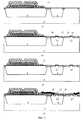
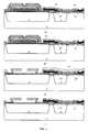
На фиг. 1а-г, фиг. 2а-г и фиг. 3а-г показы основные этапы способа изготовления интегрального датчика с чувствительным элементом в виде поликремниевой поверхностной микромеханической структуры при использовании КМОП-схемы обработки. In FIG. 1a-d, FIG. 2a-d and FIG. 3a-d show the basic steps of a method for manufacturing an integrated sensor with a sensitive element in the form of a polysilicon surface micromechanical structure using a CMOS processing circuit.
После формирования в монокристаллической кремниевой подложке n-типа 1 областей кармана p-типа 2, формирования окисла 3 термическим способом и осаждения слоя нитрида кремния 4 осаждают слой легированного поликристаллического кремния, из которого формируют соединения 5 между поликремниевой структурой и схемой. Затем осаждают опорный слой окисла кремния 6, в котором вскрывают окна 7 к соединениям 5. Далее осаждают слой поликремния и легируют его. Затем из него формируют поликремниевую структуру 8, которую отжигают при температуре 1100 - 1200oC в атмосфере азота или другого газа, который не вступает в химическую реакцию с поликремнием, в интервале времени не менее 5 минут. Затем осаждают защитный слой окисла 9 и вскрывают область схемы 10. После этого формируют охранные области 11 и диэлектрическую изоляцию 12 - фиг. 1.After the p-type 2 pocket regions are formed in the n-type 1 single crystal silicon substrate, the oxide 3 is thermally formed and the silicon nitride layer 4 is deposited, the doped polycrystalline silicon layer is deposited, from which
Затем удаляют нитрид кремния 4 с области схемы 10 таким образом, что между краем защитного слоя окисла 9 и ближайшей к нему областью диэлектрической изоляции остается область нитрида кремния 13. Затем формируют затворы 14 и области стоков и истоков 15. После этого вскрывают соединения 5 между поликремниевой структурой и схемой. Затем осаждают слой изолирующего окисла кремния 16, вскрывают в нем контактные окна 17 и формируют металлизацию 18 - фиг. 2. Then silicon nitride 4 is removed from the region of circuit 10 in such a way that between the edge of the oxide protective layer 9 and the region of dielectric insulation nearest to it there remains the region of
После этого осаждают слой пассивирующего фосфоросиликатного стекла 19 и в нем вскрывают контактные площадки 20. Затем производят разделительное вскрытие окисных слоев 21 до слоя нитрида кремния 4 и соединений 5. Затем маскируют область схемы фоторезистом 22, селективно удаляют слои пассивирующего 19, изолирующего 16 и защитного 9 окислов и селективно вытравливают опорный слой окисла 6. После этого удаляют маскирующий слой 22 - фиг. 3. After this, a layer of passivating
В предлагаемом способе изготовления за счет использования высокотемпературного отжига достигается частичная или полная рекристаллизация пленки поликремния, из которой формируют поликремниевую структуру. Рекристаллизация пленки поликремния приводит к уменьшению в ней величины внутренних механических напряжений и их неравномерности по толщине. Это уменьшает величину изгиба поликремниевых поверхностных миркомеханических структур и позволяет формировать такие структуры с большим отношением длины к ширине и, следовательно, с большей чувствительностью к механическому воздействию. In the proposed manufacturing method due to the use of high-temperature annealing, partial or complete recrystallization of the polysilicon film is achieved, from which the polysilicon structure is formed. Recrystallization of a polysilicon film leads to a decrease in the value of internal mechanical stresses and their non-uniformity in thickness. This reduces the bending of polysilicon surface world-mechanical structures and allows the formation of such structures with a large ratio of length to width and, therefore, with greater sensitivity to mechanical stress.
Источники, использованные при составлении заявки
1. Фрэнк Гудинаф. Емкостный датчик ускорения, выполненный на основе сочетания объемных и поверхностных микроструктур. - Электроника, 1993, N 11 - 12, с. 86 и 87.Sources used in the preparation of the application
1. Frank Goodinaf. Capacitive acceleration sensor, made on the basis of a combination of bulk and surface microstructures. - Electronics, 1993, N 11 - 12, p. 86 and 87.
2. Фрэнк Гудинаф. Интегральный датчик ускорения для автомобильных надувных подушек безопасности. - 1991, N 16, с. 7 - 14. 2. Frank Goodinaf. Integral acceleration sensor for car airbags. - 1991,
3. Core T. , Tsang W., Sherman S. Fabrication technology for an integrated surface-micromachined sensor. Solid State Technology. - October 1996, 39 - 47. 3. Core T., Tsang W., Sherman S. Fabrication technology for an integrated surface-micromachined sensor. Solid State Technology. - October 1996, 39 - 47.
Claims (1)
Translated fromRussianPriority Applications (1)
| Application Number | Priority Date | Filing Date | Title |
|---|---|---|---|
| RU96120054ARU2123220C1 (en) | 1996-10-07 | 1996-10-07 | Integrated transducer manufacturing process |
Applications Claiming Priority (1)
| Application Number | Priority Date | Filing Date | Title |
|---|---|---|---|
| RU96120054ARU2123220C1 (en) | 1996-10-07 | 1996-10-07 | Integrated transducer manufacturing process |
Publications (2)
| Publication Number | Publication Date |
|---|---|
| RU2123220C1true RU2123220C1 (en) | 1998-12-10 |
| RU96120054A RU96120054A (en) | 1999-01-20 |
Family
ID=20186338
Family Applications (1)
| Application Number | Title | Priority Date | Filing Date |
|---|---|---|---|
| RU96120054ARU2123220C1 (en) | 1996-10-07 | 1996-10-07 | Integrated transducer manufacturing process |
Country Status (1)
| Country | Link |
|---|---|
| RU (1) | RU2123220C1 (en) |
Citations (3)
| Publication number | Priority date | Publication date | Assignee | Title |
|---|---|---|---|---|
| EP0138023A2 (en)* | 1983-09-07 | 1985-04-24 | Nissan Motor Co., Ltd. | Semiconductor vibration detection device with lever structure |
| US4918032A (en)* | 1988-04-13 | 1990-04-17 | General Motors Corporation | Method for fabricating three-dimensional microstructures and a high-sensitivity integrated vibration sensor using such microstructures |
| RU2006993C1 (en)* | 1992-09-24 | 1994-01-30 | Акционерная компания "Технологический центр" | Integrated beam strain-measurement converter |
- 1996
- 1996-10-07RURU96120054Apatent/RU2123220C1/enactive
Patent Citations (3)
| Publication number | Priority date | Publication date | Assignee | Title |
|---|---|---|---|---|
| EP0138023A2 (en)* | 1983-09-07 | 1985-04-24 | Nissan Motor Co., Ltd. | Semiconductor vibration detection device with lever structure |
| US4918032A (en)* | 1988-04-13 | 1990-04-17 | General Motors Corporation | Method for fabricating three-dimensional microstructures and a high-sensitivity integrated vibration sensor using such microstructures |
| RU2006993C1 (en)* | 1992-09-24 | 1994-01-30 | Акционерная компания "Технологический центр" | Integrated beam strain-measurement converter |
Non-Patent Citations (1)
| Title |
|---|
| Фрэнк Гудинаф. Интегральный датчик ускорения для автомобильных надувных подушек безопасности. Электроника. - 1991, N 16, с.7-14.* |
Similar Documents
| Publication | Publication Date | Title |
|---|---|---|
| JP4138036B2 (en) | Method for manufacturing monolithic semiconductor device with integrated surface microfabrication structure | |
| JP3367113B2 (en) | Acceleration sensor | |
| JP3493068B2 (en) | Acceleration sensor made of crystalline material and method for manufacturing this acceleration sensor | |
| US5326726A (en) | Method for fabricating monolithic chip containing integrated circuitry and suspended microstructure | |
| EP1417151B1 (en) | Method for the fabrication of suspended porous silicon microstructures and application in gas sensors | |
| US5059543A (en) | Method of manufacturing thermopile infrared detector | |
| JP3033412B2 (en) | Method for manufacturing semiconductor device | |
| JPH10148624A (en) | Semiconductor integrated circuit device including chemical resistance gas microsensor and method of manufacturing the same | |
| JP3315730B2 (en) | Piezoresistive semiconductor sensor gauge and method of making same | |
| JPH10335676A (en) | Semiconductor structure with single crystal member lying above cavity provided to semiconductor board and process therefor | |
| JPH09321318A (en) | Semiconductor device with movable gate | |
| RU2123220C1 (en) | Integrated transducer manufacturing process | |
| JP2000233400A (en) | Integrated device including electromechanical microstructure without residual stress and method of manufacturing the same | |
| EP0646246B1 (en) | Method for fabricating monolithic chip containing integrated circuitry and self-supporting microstructure | |
| JPH11220137A (en) | Semiconductor pressure sensor and manufacture thereof | |
| JPH11186566A (en) | Manufacturing method of micro device | |
| JPH08264844A (en) | Floating membrane | |
| JP3343901B2 (en) | Vibration transducer and manufacturing method thereof | |
| JPH06196722A (en) | Semiconductor accelerometer and manufacture thereof | |
| JPS61212052A (en) | Semiconductor device with beam structure | |
| US6953716B2 (en) | Polysilicon material and semiconductor devices formed therefrom | |
| JPH06196721A (en) | Semiconductor accelerometer and manufacture thereof | |
| JP2005005678A (en) | Semiconductor device and its manufacturing method | |
| CN114684775B (en) | Semiconductor structure and method for forming the same | |
| JP2639153B2 (en) | Method for manufacturing semiconductor device |