RU2105379C1 - Process of production of continuous film with diamond-like structure and gear for its implementation - Google Patents
Process of production of continuous film with diamond-like structure and gear for its implementationDownload PDFInfo
- Publication number
- RU2105379C1 RU2105379C1RU94034306/25ARU94034306ARU2105379C1RU 2105379 C1RU2105379 C1RU 2105379C1RU 94034306/25 ARU94034306/25 ARU 94034306/25ARU 94034306 ARU94034306 ARU 94034306ARU 2105379 C1RU2105379 C1RU 2105379C1
- Authority
- RU
- Russia
- Prior art keywords
- solenoid
- diaphragm
- substrate
- diameter
- distance
- Prior art date
Links
- 238000000034methodMethods0.000titleclaimsabstractdescription51
- 238000004519manufacturing processMethods0.000titleabstractdescription7
- 239000000758substrateSubstances0.000claimsabstractdescription72
- 239000007789gasSubstances0.000claimsabstractdescription29
- 239000000203mixtureSubstances0.000claimsabstractdescription23
- 239000010409thin filmSubstances0.000claimsabstractdescription10
- 230000004907fluxEffects0.000claimsabstractdescription9
- 239000000126substanceSubstances0.000claimsabstractdescription7
- 239000003302ferromagnetic materialSubstances0.000claimsabstractdescription6
- 238000006073displacement reactionMethods0.000claimsabstractdescription3
- OKTJSMMVPCPJKN-UHFFFAOYSA-NCarbonChemical compound[C]OKTJSMMVPCPJKN-UHFFFAOYSA-N0.000claimsdescription14
- 229910052799carbonInorganic materials0.000claimsdescription14
- 150000004767nitridesChemical class0.000claimsdescription5
- 150000001247metal acetylidesChemical class0.000claimsdescription3
- 239000010408filmSubstances0.000abstractdescription84
- 230000008021depositionEffects0.000abstractdescription7
- 230000000694effectsEffects0.000abstractdescription5
- 210000002381plasmaAnatomy0.000description19
- 239000000463materialSubstances0.000description17
- 230000005291magnetic effectEffects0.000description14
- 229910003460diamondInorganic materials0.000description11
- 239000010432diamondSubstances0.000description11
- XUIMIQQOPSSXEZ-UHFFFAOYSA-NSiliconChemical compound[Si]XUIMIQQOPSSXEZ-UHFFFAOYSA-N0.000description8
- 229910052710siliconInorganic materials0.000description8
- 239000010703siliconSubstances0.000description8
- UHOVQNZJYSORNB-UHFFFAOYSA-NBenzeneChemical compoundC1=CC=CC=C1UHOVQNZJYSORNB-UHFFFAOYSA-N0.000description6
- 238000000151depositionMethods0.000description6
- 238000002360preparation methodMethods0.000description6
- XKRFYHLGVUSROY-UHFFFAOYSA-NArgonChemical compound[Ar]XKRFYHLGVUSROY-UHFFFAOYSA-N0.000description5
- 238000009826distributionMethods0.000description5
- 239000002245particleSubstances0.000description5
- 229910001220stainless steelInorganic materials0.000description5
- 239000010935stainless steelSubstances0.000description5
- IJGRMHOSHXDMSA-UHFFFAOYSA-NAtomic nitrogenChemical compoundN#NIJGRMHOSHXDMSA-UHFFFAOYSA-N0.000description4
- VNWKTOKETHGBQD-UHFFFAOYSA-NmethaneChemical compoundCVNWKTOKETHGBQD-UHFFFAOYSA-N0.000description4
- 230000003746surface roughnessEffects0.000description4
- 150000001875compoundsChemical class0.000description3
- 229910002804graphiteInorganic materials0.000description3
- 239000010439graphiteSubstances0.000description3
- 238000010438heat treatmentMethods0.000description3
- 229930195733hydrocarbonNatural products0.000description3
- 150000002430hydrocarbonsChemical class0.000description3
- 229910052582BNInorganic materials0.000description2
- ZOXJGFHDIHLPTG-UHFFFAOYSA-NBoronChemical compound[B]ZOXJGFHDIHLPTG-UHFFFAOYSA-N0.000description2
- 229910052581Si3N4Inorganic materials0.000description2
- 229910052786argonInorganic materials0.000description2
- 229910052796boronInorganic materials0.000description2
- 238000005229chemical vapour depositionMethods0.000description2
- 238000004140cleaningMethods0.000description2
- 238000002485combustion reactionMethods0.000description2
- 238000010894electron beam technologyMethods0.000description2
- 238000001493electron microscopyMethods0.000description2
- 239000001257hydrogenSubstances0.000description2
- 229910052739hydrogenInorganic materials0.000description2
- 239000011261inert gasSubstances0.000description2
- 239000012212insulatorSubstances0.000description2
- 150000002500ionsChemical class0.000description2
- 229910052751metalInorganic materials0.000description2
- 239000002184metalSubstances0.000description2
- 229910052757nitrogenInorganic materials0.000description2
- 230000005855radiationEffects0.000description2
- HQVNEWCFYHHQES-UHFFFAOYSA-Nsilicon nitrideChemical compoundN12[Si]34N5[Si]62N3[Si]51N64HQVNEWCFYHHQES-UHFFFAOYSA-N0.000description2
- 239000000243solutionSubstances0.000description2
- PZNSFCLAULLKQX-UHFFFAOYSA-NBoron nitrideChemical compoundN#BPZNSFCLAULLKQX-UHFFFAOYSA-N0.000description1
- 239000004215Carbon black (E152)Substances0.000description1
- UGFAIRIUMAVXCW-UHFFFAOYSA-NCarbon monoxideChemical compound[O+]#[C-]UGFAIRIUMAVXCW-UHFFFAOYSA-N0.000description1
- RYGMFSIKBFXOCR-UHFFFAOYSA-NCopperChemical compound[Cu]RYGMFSIKBFXOCR-UHFFFAOYSA-N0.000description1
- UFHFLCQGNIYNRP-UHFFFAOYSA-NHydrogenChemical compound[H][H]UFHFLCQGNIYNRP-UHFFFAOYSA-N0.000description1
- 229910000831SteelInorganic materials0.000description1
- 238000010521absorption reactionMethods0.000description1
- 239000000654additiveSubstances0.000description1
- 229910003481amorphous carbonInorganic materials0.000description1
- 230000015572biosynthetic processEffects0.000description1
- 238000004364calculation methodMethods0.000description1
- 229910002091carbon monoxideInorganic materials0.000description1
- 238000005234chemical depositionMethods0.000description1
- 239000010949copperSubstances0.000description1
- 229910052802copperInorganic materials0.000description1
- 230000007547defectEffects0.000description1
- 239000003989dielectric materialSubstances0.000description1
- 230000005684electric fieldEffects0.000description1
- 238000000572ellipsometryMethods0.000description1
- 238000005265energy consumptionMethods0.000description1
- 238000005516engineering processMethods0.000description1
- 239000011521glassSubstances0.000description1
- 125000004435hydrogen atomChemical class[H]*0.000description1
- 238000002347injectionMethods0.000description1
- 239000007924injectionSubstances0.000description1
- 238000002844meltingMethods0.000description1
- 238000004377microelectronicMethods0.000description1
- 238000001000micrographMethods0.000description1
- 230000003287optical effectEffects0.000description1
- 238000004157plasmatronMethods0.000description1
- 229920000642polymerPolymers0.000description1
- 239000003870refractory metalSubstances0.000description1
- 229910052702rheniumInorganic materials0.000description1
- WUAPFZMCVAUBPE-UHFFFAOYSA-Nrhenium atomChemical compound[Re]WUAPFZMCVAUBPE-UHFFFAOYSA-N0.000description1
- 239000004065semiconductorSubstances0.000description1
- 230000035945sensitivityEffects0.000description1
- HBMJWWWQQXIZIP-UHFFFAOYSA-Nsilicon carbideChemical compound[Si+]#[C-]HBMJWWWQQXIZIP-UHFFFAOYSA-N0.000description1
- 229910010271silicon carbideInorganic materials0.000description1
- 238000005507sprayingMethods0.000description1
- 239000010959steelSubstances0.000description1
- 238000004381surface treatmentMethods0.000description1
- 231100000331toxicToxicity0.000description1
- 230000002588toxic effectEffects0.000description1
- WFKWXMTUELFFGS-UHFFFAOYSA-NtungstenChemical compound[W]WFKWXMTUELFFGS-UHFFFAOYSA-N0.000description1
- 229910052721tungstenInorganic materials0.000description1
- 239000010937tungstenSubstances0.000description1
- 238000009827uniform distributionMethods0.000description1
- XLYOFNOQVPJJNP-UHFFFAOYSA-NwaterChemical compoundOXLYOFNOQVPJJNP-UHFFFAOYSA-N0.000description1
- 230000003313weakening effectEffects0.000description1
Images


Landscapes
- Crystals, And After-Treatments Of Crystals (AREA)
- Chemical Vapour Deposition (AREA)
Abstract
Description
Translated fromRussianИзобретение относится к тонким пленкам с алмазоподобной структурой, способам и устройствам для их получения из плазмы сверхвысокочастотного разряда (СВЧ-плазмы) в режиме электронно-циклотронного резонанса (ЭЦР) и может быть использовано в различных отраслях микроэлектроники, оптики и точной механики, а также в медицинской технике. The invention relates to thin films with a diamond-like structure, methods and devices for their production from microwave plasma discharge (microwave plasma) in electron-cyclotron resonance (ECR) mode and can be used in various branches of microelectronics, optics and precision mechanics, as well as in medical equipment.
Тонкие пленки с алмазоподобной и алмазной структурой широко применяются в настоящее время благодаря своим свойствам - сверхтвердости, высокой износостойкости и теплопроводности, малому поглощению в оптическом диапазоне и уникальным электрофизическим свойствам. Применение в современных приборах накладывает жесткие требования к этим пленкам: минимальная шероховатость и высокая однородность, а также возможность использования в качестве подложек для таких пленок, как материалов, обладающих высокой термической устойчивостью, так и материалов, не имеющих таковой. Особый интерес представляет получение сплошных пленок толщиной порядка нескольких нанометров, поскольку большинство материалов в этих условиях при традиционных способах напыления образуют лишь островковые пленки. Thin films with a diamond-like and diamond structure are widely used at present due to their properties - superhardness, high wear resistance and thermal conductivity, low absorption in the optical range and unique electrophysical properties. Application in modern devices imposes stringent requirements on these films: minimal roughness and high uniformity, as well as the possibility of using as substrates for such films as materials with high thermal stability, and materials that do not. Of particular interest is the preparation of continuous films with a thickness of the order of several nanometers, since most materials under these conditions under traditional spraying methods form only island films.
Свойства и качество получаемых пленок в большей или меньшей степени зависят от условий их получения, поэтому важно разработать простой и надежный способ получения таких пленок. The properties and quality of the resulting films to a greater or lesser extent depend on the conditions for their preparation, therefore it is important to develop a simple and reliable method for producing such films.
Известен способ получения алмазоподобной углеродной пленки из СВЧ-плазмы в режиме ЭЦР, обладающей высокой адгезией к подложке [1]. В качестве рабочего газа использован бензол, рабочее давление в технологической камере > 10-3 Toрp (0,1 Па), на подложку подают отрицательное электрическое смещение не более 300 В. Недостатком этого способа является его сложность, связанная с необходимостью очистки отходящих газов от токсичного и легковоспламеняющегося бензола. Обеспечивая высокую скорость осаждения пленки, данный способ, однако, не гарантирует ее высокую однородность, минимальную шероховатость, а также не позволяет получать другие пленки с алмазоподобной структурой, такие как, например, нитриды бора, кремния, карбид кремния и др.A known method of producing a diamond-like carbon film from a microwave plasma in ECR mode, with high adhesion to the substrate [1]. Benzene was used as the working gas, the working pressure in the process chamber> 10-3 Torr (0.1 Pa), a negative electric displacement of not more than 300 V was applied to the substrate. The disadvantage of this method is its complexity, which is associated with the need to clean the exhaust gases from toxic and flammable benzene. Providing a high film deposition rate, this method, however, does not guarantee its high uniformity, minimal roughness, and also does not allow obtaining other films with a diamond-like structure, such as, for example, boron nitride, silicon nitride, silicon carbide, etc.
Известен способ получения алмазоподобной пленки из СВЧ-плазмы в режиме ЭЦР [2]. Недостатком данного способа является неоднородность получаемой пленки из-за значительных включений пироуглерода и графита, большая шероховатость пленки, невозможность получения пленок других алмазоподобных материалов. A known method of producing a diamond-like film from a microwave plasma in ECR mode [2]. The disadvantage of this method is the heterogeneity of the resulting film due to significant inclusions of pyrocarbon and graphite, a large roughness of the film, the inability to obtain films of other diamond-like materials.
Наиболее близким к предложенному способу является способ получения алмазоподобной углеродной пленки, включающий ее нанесение в вакууме из плазмы СВЧ-разряда в режиме ЭЦР при подаче электрического смещения на подложку [3]. Недостатком способа является неоднородность полученной пленки из-за значительных включений пироуглерода и аморфного углерода, значительная шероховатость пленки, связанная с образованием микрокристаллитов. Это происходит вследствие высокой плотности СВЧ-мощности, высоких давления и температуры подложки. Указанный способ неприемлем для получения пленок других материалов с алмазоподобной структурой. Closest to the proposed method is a method for producing a diamond-like carbon film, including applying it in vacuum from a microwave plasma discharge in ECR mode by applying an electric bias to the substrate [3]. The disadvantage of this method is the heterogeneity of the obtained film due to significant inclusions of pyrocarbon and amorphous carbon, a significant roughness of the film associated with the formation of microcrystallites. This is due to the high density of microwave power, high pressure and substrate temperature. The specified method is not acceptable for obtaining films of other materials with a diamond-like structure.
Известные способы реализуются с помощью различных устройств, описанных, например, в [2,3,4], конструктивные особенности которых приводят к вышеуказанным недостаткам пленок и способов их получения. Known methods are implemented using various devices described, for example, in [2,3,4], the design features of which lead to the above-mentioned disadvantages of films and methods for their preparation.
Наиболее близким к заявленному устройству является устройство для нанесения алмазных, алмазоподобных и металлических пленок из СВЧ-плазмы в режиме ЭЦР [5]. Оно содержит источник СВЧ-энергии, цилиндрический волновод с поперечным герметичным диэлектрическим окном, герметичную технологическую камеру с системой вакуумирования и напуска рабочих газов, держателем подложки, электрически изолированным от технологической камеры и два соленоида, соосные с волноводом, один из которых расположен в плоскости диэлектрического окна, а второй - между первым соленоидом и держателем подложки. Это устройство позволяет получать тонкие пленки с алмазоподобной структурой различного состава: углеродные, нитридов кремния, бора и т.д., однако эти пленки неоднородны по фазовому составу, их значительная шероховатость является следствием недостаточно равномерного распределения магнитного поля, создаваемого в устройстве. Closest to the claimed device is a device for applying diamond, diamond-like and metal films from microwave plasma in ECR mode [5]. It contains a microwave energy source, a cylindrical waveguide with a transverse sealed dielectric window, a sealed process chamber with a vacuum and gas injection system, a substrate holder electrically isolated from the process chamber, and two solenoids coaxial with the waveguide, one of which is located in the plane of the dielectric window and the second between the first solenoid and the substrate holder. This device allows to obtain thin films with a diamond-like structure of various compositions: carbon, silicon nitride, boron, etc., however, these films are inhomogeneous in phase composition, their significant roughness is a consequence of the insufficiently uniform distribution of the magnetic field generated in the device.
Известные способы нанесения позволяют получать тонкие пленки алмазоподобных материалов из плазмы газового разряда. Известна гладкая алмазная пленка, полученная методом химического газофазного осаждения из СВЧ-плазмы [6] . При толщине пленки 10 мкм ее шероховатость не превышает 30 нм. Недостатком этой пленки является то, что ее кристаллическая структура, а следовательно, и шероховатость поверхности, в значительной степени зависят от условий осаждения. Температура осаждения, как правило, превышает 730oC, что ограничивает материалы, которые могут быть использованы в качестве подложек. К недостаткам указанной пленки также следует отнести то, что для пленки с толщиной, отличающейся от 10 мкм, шероховатость поверхности превышает 30 нм. Известны пленки с алмазомодобной структурой из нитридов бора, кремния и т.д. [4] . Эти пленки могут быть получены при более низких температурах, однако они неоднородны, имеют большое количество загрязняющих включений неалмазоподобной фазы и их шероховатость превышает 30 нм независимо от толщины пленок. Особый интерес представляет получение сплошных сверхтонких алмазоподобных пленок на различных материалах. Так, например, известна нанокристаллическая алмазная пленка [7]. Шероховатость поверхности указанной пленки не превышает 30 нм, а в которых случаях лежит в пределах 20 нм и в меньшей степени зависит от условий ее осаждения. Недостатком данной пленки является, как и в первом случае, высокая температура осаждения и ограниченный круг материалов для подложек, присутствие графитовой фазы, а также большая толщина: 1-10 мкм, что ограничивает область ее применения.Known methods of application allow to obtain thin films of diamond-like materials from a gas discharge plasma. Known smooth diamond film obtained by chemical vapor deposition from a microwave plasma [6]. With a film thickness of 10 μm, its roughness does not exceed 30 nm. The disadvantage of this film is that its crystalline structure, and hence the surface roughness, largely depends on the deposition conditions. The deposition temperature, as a rule, exceeds 730o C, which limits the materials that can be used as substrates. The disadvantages of this film should also include the fact that for a film with a thickness other than 10 μm, the surface roughness exceeds 30 nm. Known films with a diamond-like structure of boron nitrides, silicon, etc. [4] . These films can be obtained at lower temperatures, however, they are heterogeneous, have a large number of contaminating inclusions of a non-diamond-like phase, and their roughness exceeds 30 nm, regardless of the thickness of the films. Of particular interest is the preparation of continuous ultrathin diamond-like films on various materials. For example, a nanocrystalline diamond film is known [7]. The surface roughness of the specified film does not exceed 30 nm, and in which cases lies within 20 nm and to a lesser extent depends on the conditions of its deposition. The disadvantage of this film is, as in the first case, a high deposition temperature and a limited range of substrate materials, the presence of a graphite phase, and also a large thickness: 1-10 μm, which limits its scope.
Изложенное дает основание сделать вывод о том, что известные пленки не в полной мере удовлетворяют современным требованиям, а известные способы и устройства не позволяют получать гладкие, однородные, т.е. без посторонних включений, пленки с алмазоподобной структурой и шероховатостью менее 20 нм на уровне, соответствующем пределу чувствительности современных методов ее контроля. Интенсивные термические воздействия на подложку не позволяют использовать в качестве таковых материалы с низкой термической устойчивостью, что ограничивает выбор материалов подложек и в области применения таких пленок. The foregoing gives reason to conclude that the known films do not fully meet modern requirements, and the known methods and devices do not allow to obtain smooth, uniform, i.e. without foreign inclusions, films with a diamond-like structure and roughness of less than 20 nm at a level corresponding to the sensitivity limit of modern methods of its control. Intensive thermal effects on the substrate do not allow the use of materials with low thermal stability as such, which limits the choice of substrate materials in the field of application of such films.
В основу настоящего изобретения положена задача получения тонких нанометровых пленок с алмазоподобной структурой, лишенных указанных недостатков, и разработки способа получения таких пленок, позволяющего ослабить термическое воздействие на подложку при обеспечении устойчивого горения СВЧ-разряда в режиме ЭЦР при низком давлении и малой мощности, подводимой к устройству, начиная от 40 Вт и выше. Дополнительным техническим результатом заявленного изобретения является уменьшение габаритов и потребляемой мощности устройства при высоком качестве получаемых пленок. Предложенное устройство также позволяет обрабатывать подложки большой площади и произвольной конфигурации. The present invention is based on the task of producing thin nanometer films with a diamond-like structure, devoid of these drawbacks, and to develop a method for producing such films that can reduce the thermal effect on the substrate while ensuring stable combustion of the microwave discharge in the ECR mode at low pressure and low power supplied to device starting from 40 W and above. An additional technical result of the claimed invention is to reduce the size and power consumption of the device with high quality films. The proposed device also allows you to process substrates of a large area and arbitrary configuration.
Это достигается способом получения сплошной тонкой пленки с алмазоподобной структурой, исключающим нанесение на подложку из плазмы СВЧ-разряда в режиме ЭЦР в атмосфере рабочего газа или смеси газов при подаче отрицательного электрического смещения на подложку, расположенную вне зоны ЭЦР, при давлении в пределах 0,01 - 10 Па плотности потока мощности, подводимой в зону ЭЦР - 0,2-5 Вт/см2. С целью получения равномерной по толщине сплошной тонкой пленки подложку необходимо помещать на расстоянии от зоны ЭЦР не менее одного ее характерного линейного размера, т.е. максимального размера подложки в плоскости, перпендикулярной оси волновода-плазматрона. Низкие рабочее давление и плотность вводимой СВЧ-мощности позволяют избежать нагрева подложек до температур выше 50oC, вследствие чего пленки оказывается возможным наносить на материалы, термически неустойчивые при более высоких температурах: полимеры, легкоплавкие стекла, бумагу и т.д. При этом вследствие больших длин пробега активных частиц плазмы при низких давлениях площадь обрабатываемой поверхности ограничивается только конструктивными особенностями технологической камеры, а подложки могут иметь весьма сложную форму, в отличие от традиционно использующихся в известных способах плоских пластин. В использованной при практических испытаниях конструкции технологической камеры характерный линейный размер подложки не превышал 250 мм (диаметра вакуумной камеры). При получении алмазных или углеродных алмазоподобных пленок в качестве рабочего газа или, по крайней мере, одного из компонентов смеси газов используют углеродсодержащий газ (например, метан, смеси его с водородом и т. п.). При получении пленок нитридов в качестве компонентов смеси газов используют вещества, содержащие элементы, образующие нитриды (например, смеси азота с парами соединений соответствующего нитридообразующего элемента). При получении пленок карбидов в качестве компонентов смеси газов используют вещества, содержащие элементы, образующие карбиды (например, смеси углеводородов с парами летучих соединений карбидообразующих элементов: бора, кремния и т.п.). В качестве варианта технологического режима в рабочую газовую смесь можно добавлять инертный газ, например аргон.This is achieved by the method of producing a continuous thin film with a diamond-like structure, which excludes the deposition of a microwave discharge on a substrate from a microwave plasma in an ECR mode in an atmosphere of a working gas or gas mixture when a negative electric bias is applied to a substrate located outside the ECR zone at a pressure in the range of 0.01 - 10 Pa power flux density supplied to the ECR zone - 0.2-5 W / cm2 . In order to obtain a uniform thin film continuous in thickness, the substrate must be placed at a distance from the ECR zone of at least one of its characteristic linear dimensions, i.e. the maximum size of the substrate in a plane perpendicular to the axis of the waveguide-plasmatron. Low working pressure and the density of the input microwave power to avoid heating the substrates to temperatures above 50o C, as a result of which it is possible to apply films to materials that are thermally unstable at higher temperatures: polymers, low-melting glass, paper, etc. Moreover, due to the long mean free paths of active plasma particles at low pressures, the surface area to be treated is limited only by the design features of the process chamber, and the substrates can have a very complex shape, in contrast to the flat plates traditionally used in the known methods. In the design of the technological chamber used in practical tests, the characteristic linear size of the substrate did not exceed 250 mm (diameter of the vacuum chamber). Upon receipt of diamond or carbon diamond-like films, carbon-containing gas is used as a working gas or at least one of the components of the gas mixture (for example, methane, mixtures thereof with hydrogen, etc.). Upon receipt of nitride films, substances containing elements forming nitrides (for example, nitrogen mixtures with pairs of compounds of the corresponding nitride-forming element) are used as components of a gas mixture. In the preparation of carbide films, substances containing elements forming carbides are used as components of a gas mixture (for example, mixtures of hydrocarbons with vapors of volatile compounds of carbide-forming elements: boron, silicon, etc.). Alternatively, an inert gas, such as argon, can be added to the working gas mixture.
При давлении, меньшем 0,01 Па, не удается поддерживать устойчивый разряд по всей площади сечения технологической камеры, что ухудшает качество получаемых пленок. При давлении, большем 10 Па, газовая температура СВЧ-плазмы значительно увеличивается, что вызывает разогрев подложки и ограничивает выбор применимых в качестве таковой материалов. At a pressure of less than 0.01 Pa, it is not possible to maintain a stable discharge over the entire cross-sectional area of the process chamber, which affects the quality of the resulting films. At a pressure greater than 10 Pa, the gas temperature of the microwave plasma increases significantly, which causes the substrate to heat up and limits the choice of materials suitable as such.
Расчет плотности СВЧ-мощности, подводимой в зону ЭЦР, производят исходя из следующих предпосылок. Удельная мощность P, поглощаемая единицей объема материала, находящегося в СВЧ-поле с напряженностью E, равна
P = kfE2ε•tgδ,(Вт/см3) (1) ,
где k - поправочный коэффициент, зависящий от системы единиц (СИ, СГС и т.д.);
f - частота излучения, Гц;
E - напряженность электрического поля. В/см;
ε - относительная диэлектрическая проницаемость материала;
tgδ - тангенс угла диэлектрических потерь.The calculation of the density of the microwave power supplied to the ECR zone is carried out on the basis of the following premises. The specific power P absorbed by a unit volume of a material located in a microwave field with intensity E is equal to
P = kfE2 ε • tanδ, (W / cm3 ) (1),
where k is the correction factor depending on the system of units (SI, GHS, etc.);
f is the radiation frequency, Hz;
E is the electric field strength. W / cm;
ε is the relative dielectric constant of the material;
tanδ is the dielectric loss tangent.
Из формулы (1) следует, что для полупроводниковых и диэлектрических материалов мощность, поглощаемая единицей объема, пропорциональна E2, т.е. плотности потока СВЧ-мощности, что сказывается, прежде всего, на разогреве материала подложки. При плотности потока СВЧ-мощности более 5 Вт/см2 температура подложки может превысить порог ее термической устойчивости. При плотности потока СВЧ-мощности менее 0,2 Вт/см2 не удается поддерживать устойчивый СВЧ-разряд.From formula (1) it follows that for semiconductor and dielectric materials, the power absorbed by a unit volume is proportional to E2 , i.e. microwave power flux density, which affects, first of all, the heating of the substrate material. When the flux density of the microwave power is more than 5 W / cm2, the temperature of the substrate can exceed the threshold of its thermal stability. When the flux density of the microwave power is less than 0.2 W / cm2 it is not possible to maintain a stable microwave discharge.
Важным фактором является место расположения подложки. Если расположить подложку на расстоянии от зоны ЭЦР менее одного ее характерного линейного размера, то плотность потока частиц, падающих из плазмы, будет недостаточно равномерной для получения однородной пленки. An important factor is the location of the substrate. If the substrate is located at a distance from the ECR zone of less than one of its characteristic linear dimensions, then the flux density of particles incident from the plasma will not be uniform enough to produce a uniform film.
Предложенный способ реализуется в устройстве для получения тонкой сплошной пленки с алмазоподобной структурой из плазмы СВЧ-разряда в режиме ЭЦР, включающем источник СВЧ-энергии, связанный с герметичной технологической камерой через цилиндрический волновод, и два соленоида, соосных с волноводом. Волновод снабжен герметичным диэлектрическим окном, а в технологической камере размещается держатель подложки, электрически изолированный от камеры. Первый соленоид размещен в плоскости диэлектрического окна для его защиты от потока плазмы, а второй - для формирования зоны ЭЦР - между первым соленоидом и держателем подложки. Устройство дополнительно снабжено диафрагмой из ферромагнитного материала, расположенной соосно с волноводом между вторым соленоидом и держателем подложки, причем расстояние между диафрагмой и вторым соленоидом не превышает внутреннего диаметра второго соленоида, а диаметр отверстия этой диафрагмы выполнен в соответствии с условием, обеспечивающим оптимальную конфигурацию магнитного поля в зоне горения ЭЦР-разряда:
где Dнволн - наружный диаметр волновода, см;
d1д - диаметр отверстия диафрагмы, см;
D2вн, D2нар - соответственно внутренний и наружный диаметры второго соленоида, см.The proposed method is implemented in a device for producing a thin continuous film with a diamond-like structure from a microwave discharge plasma in ECR mode, which includes a microwave energy source connected to a sealed process chamber through a cylindrical waveguide, and two solenoids coaxial with the waveguide. The waveguide is equipped with a sealed dielectric window, and a substrate holder, electrically isolated from the camera, is placed in the process chamber. The first solenoid is placed in the plane of the dielectric window to protect it from the plasma flow, and the second - to form an ECR zone - between the first solenoid and the substrate holder. The device is additionally equipped with a diaphragm made of ferromagnetic material located coaxially with the waveguide between the second solenoid and the substrate holder, the distance between the diaphragm and the second solenoid not exceeding the inner diameter of the second solenoid, and the hole diameter of this diaphragm is made in accordance with the condition that ensures the optimal configuration of the magnetic field in combustion zone of an ECR discharge:
where Dnwaves - the outer diameter of the waveguide, cm;
d1d - the diameter of the aperture, cm;
D2ext , D2nar - respectively the inner and outer diameters of the second solenoid, see
Держатель подложки установлен на расстоянии от второго соленоида не менее чем один характерный линейный размер подложки. Устройство может быть дополнительно снабжено третьим соленоидом и второй диафрагмой из ферромагнитного материала для корректировки магнитного поля в зоне ЭЦР. Третий соленоид расположен на расстоянии от основной диафрагмы в направлении держателя подложки, удовлетворяющем условию:
L ≤ D3вн + d1д,
где L - расстояние от первой диафрагмы до третьего соленоида, см;
D3вн - внутренний диаметр третьего соленоида, см;
d1д - диаметр отверстия основной диафрагмы, см;
Вторая диафрагма расположена между основной диафрагмой и третьим соленоидом на расстоянии от третьего соленоида, не превышающем его внутренний диаметр.The substrate holder is installed at a distance from the second solenoid of at least one characteristic linear size of the substrate. The device can be additionally equipped with a third solenoid and a second diaphragm made of ferromagnetic material to adjust the magnetic field in the ECR zone. The third solenoid is located at a distance from the main diaphragm in the direction of the substrate holder, satisfying the condition:
L ≤ D3int + d1d ,
where L is the distance from the first diaphragm to the third solenoid, cm;
D3VN - inner diameter of the third solenoid, cm;
d1d - hole diameter of the main diaphragm, cm;
The second diaphragm is located between the main diaphragm and the third solenoid at a distance from the third solenoid, not exceeding its internal diameter.
Предлагаемое устройство иллюстрируется следующими чертежами. The proposed device is illustrated by the following drawings.
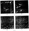
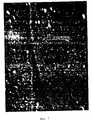
На фиг. 1 показано схематическое изображение предложенного устройства с одной диафрагмой; на фиг. 2 - распределение магнитных полей в устройстве, аналогичном предложенному, но без диафрагмы; на фиг. 3 - распределение магнитных полей в устройстве с диафрагмой, изображенном на фиг. 1; на фиг. 4 - схематическое изображение устройства с дополнительным третьим соленоидом и второй диафрагмой; на фиг. 5 - распределение магнитных полей в устройстве, изображенном на фиг. 4; на фиг. 6 - электронномикроскопические изображения: а) - углеродная пленка на нержавеющей стали; б) - свободная подложка из нержавеющей стали; в) - углеродная пленка на кремниевой подложке; г) - свободная кремниевая подложка; на фиг. 7 - граница пленки на подложке из нержавеющей стали при косом падении электронного луча. In FIG. 1 shows a schematic representation of the proposed device with a single diaphragm; in FIG. 2 - distribution of magnetic fields in a device similar to the one proposed, but without a diaphragm; in FIG. 3 shows the distribution of magnetic fields in the diaphragm device shown in FIG. one; in FIG. 4 is a schematic illustration of a device with an additional third solenoid and a second diaphragm; in FIG. 5 shows the distribution of magnetic fields in the device shown in FIG. 4; in FIG. 6 - electron microscopic images: a) - carbon film on stainless steel; b) - a free substrate of stainless steel; c) - carbon film on a silicon substrate; g) - free silicon substrate; in FIG. 7 - film boundary on a stainless steel substrate with an oblique incidence of an electron beam.
Изображенное на фиг. 1 устройство включает следующие конструктивные элементы: 1 - источник СВЧ-энергии, 2 - технологическая камера, 3 -диэлектрическое окно, 4 - цилиндрический волновод, который может быть выполнен с расширением в сторону технологической камеры, 5 - система вакуумирования, 6 - система напуска рабочих газов, 7 - держатель подложки, 8 - изолятор держателя подложки, 9 - первый соленоид, 10 - второй соленоид, 11 - диафрагма из ферромагнитного материала. Depicted in FIG. 1 device includes the following structural elements: 1 - a source of microwave energy, 2 - a technological chamber, 3 - a dielectric window, 4 - a cylindrical waveguide, which can be expanded to the side of the technological chamber, 5 - a vacuum system, 6 - a system of working inlet gases, 7 - substrate holder, 8 - insulator of the substrate holder, 9 - first solenoid, 10 - second solenoid, 11 - diaphragm made of ferromagnetic material.
Необходимость введения диафрагмы 11 поясняется с помощью фиг. 3 и 4. Распределение осевого и радиального магнитных полей на фиг. 3 таково, что образуется протяженная зона ЭЦР со значительными потоками частиц на стенки технологической камеры 2, что требует для поддержания стационарного разряда высокого уровня подводимой СВЧ-мощности и приводит к нагреву подложки до температур, превышающих порог ее термической устойчивости (см. формулу 1),
Введение диафрагмы на расстоянии от второго соленоида, превышающем его внутренний диаметр, нецелесообразно ввиду незначительности магнитных полей в этой области. Если диаметр отверстия диафрагмы будет меньше диаметра самого волновода в месте ее расположения, то это приведет к частичному отражению СВЧ-мощности, подводимой в зону ЭЦР, что не имеет смысла. При диаметре отверстия диафрагмы, превышающем среднее арифметическое из внутреннего и наружного диаметров второго соленоида (D2вн+D2нар)/2 поля вблизи диафрагмы 11 настолько малы, что ее работа становится неэффективной.The need for introducing a
The introduction of the diaphragm at a distance from the second solenoid in excess of its internal diameter is impractical due to the insignificance of the magnetic fields in this region. If the diameter of the diaphragm opening is less than the diameter of the waveguide itself at its location, this will lead to a partial reflection of the microwave power supplied to the ECR zone, which makes no sense. When the diameter of the diaphragm hole exceeds the arithmetic average of the inner and outer diameters of the second solenoid (D2ext + D2nar ) / 2 fields near the
На фиг. 4 позиции совпадают с указанными на фиг. 1, с той лишь разницей, что в устройство введен дополнительный третий соленоид 12 и вторая диафрагма 13. Эффект от введения третьего соленоида и второй диафрагмы поясняется с помощью фиг. 5. Изменяя напряженность магнитного поля, создаваемого третьим соленоидом, и местоположение второй диафрагмы, можно изменять положение зоны ЭЦР (см. фиг. 5 отрезок "а"). Это улучшает однородность пленки, а также создает возможность нанесения нанометровых пленок на подложки произвольно сложной конфигурации. Этого же эффекта можно добиться, увеличивая силу тока в соленоидах, но это приведет к значительному повышению затрат энергии в устройстве. In FIG. 4 positions coincide with those indicated in FIG. 1, with the only difference that an additional
Расположение третьего соленоида на расстоянии от первой диафрагмы, превышающем сумму его внутреннего диаметра и диаметра отверстия первой диафрагмы, приводит к ослаблению эффективности указанного соленоида. Диаметр отверстия второй диафрагмы не может быть меньше диаметра той части технологической камеры, в которой она расположена, и не может превышать среднее арифметическое из внутреннего и наружного диаметров третьего соленоида, исходя из аналогичных вышеизложенным соображений. The location of the third solenoid at a distance from the first diaphragm in excess of the sum of its inner diameter and the diameter of the opening of the first diaphragm, leads to a weakening of the effectiveness of the specified solenoid. The diameter of the hole of the second diaphragm cannot be less than the diameter of the part of the process chamber in which it is located, and cannot exceed the arithmetic average of the inner and outer diameters of the third solenoid, based on similar considerations to the foregoing.
Приемы и устройства, позволяющие регулировать магнитное поле в зоне ЭЦР, достаточно хорошо известны. В частности, в [5] магнитное поле регулируется при помощи дополнительной магнитной системы, установленной вокруг цилиндрического волновода, однако это не позволяет максимально сузить зону ЭЦР и создать условия для ее перемещения в случае необходимости. Кроме того, это значительно усложняет конструкцию устройства и приводит к дополнительным энергозатратам. Известны решения с применением стержней, решеток и корзин из графита или тугоплавкого металла (вольфрама или рения) [8] для регулирования поля в устройствах химического осаждения алмазоподобных пленок, что позволяет наносить тонкие равномерные по толщине пленки, но при этом не только усложняет конструкцию, но и создает дополнительный источник загрязнений и потерь СВЧ-энергии. Techniques and devices that allow you to adjust the magnetic field in the ECR zone are well known. In particular, in [5] the magnetic field is controlled by an additional magnetic system installed around a cylindrical waveguide, however, this does not allow to narrow the ECR zone as much as possible and create conditions for its movement if necessary. In addition, this greatly complicates the design of the device and leads to additional energy costs. Known solutions using rods, gratings and baskets made of graphite or refractory metal (tungsten or rhenium) [8] to control the field in devices for the chemical deposition of diamond-like films, which allows you to apply thin films uniform in thickness, but not only complicates the design, but and creates an additional source of pollution and loss of microwave energy.
Изложенное показывает, что в научно-технической и патентной литературе отсутствуют решения, позволяющие достичь указанных технических результатов с помощью вышеуказанных приемов и средств, что позволяет сделать вывод о соответствии заявляемого изобретения условиям патентоспособности "новизна" и "изобретательский уровень". Заявленные способ и устройство могут быть реализованы в промышленности с получением широкого спектра нанометровых пленок с алмазоподобной структурой, что позволяет сделать вывод о соответствии заявляемого изобретения условию патентоспособности "промышленная применимость". The foregoing shows that in the scientific and technical and patent literature there are no solutions that can achieve the indicated technical results using the above methods and means, which allows us to conclude that the claimed invention meets the patentability conditions of "novelty" and "inventive step". The claimed method and device can be implemented in industry to produce a wide range of nanometer films with a diamond-like structure, which allows us to conclude that the claimed invention meets the patentability condition "industrial applicability".
Заявленное устройство работает следующим образом. The claimed device operates as follows.
Подложку закрепляют на держателе 7 произвольной формы. Конструкция держателя определяется только формой и размерами подложки, на которую наносят пленку. Держатель 7 закрепляют на изоляторе 8, помещают в технологическую камеру 2 и откачивают до давления 10-4Па.The substrate is fixed on the
Подложку, прошедшую известную процедуру очистки, можно дополнительно очистить непосредственно в технологической камере 2, для чего в последнюю из системы напуска газов 6 подают аргон до давления 1 Па и с помощью источника СВЧ-энергии 1 зажигают газовый разряд. Подложка очищается за счет бомбардировки ее поверхности ионами и атомами аргона из плазмы СВЧ- разряда. После окончания очистки технологическую камеру вновь откачивают до давления 10-4Па.The substrate that has passed the known cleaning procedure can be further cleaned directly in the
Затем в технологическую камеру 2 из системы напуска 6 подают рабочую газовую смесь. Для получения углеродной алмазоподобной пленки в технологическую камеру подают метан или другой летучий углеводород в смеси с водородом или парами воды, различные смеси на основе монооксида углерода, в том числе с добавками инертных газов. В данном случае использовали смесь 7% об. CH4 и 93% об. H2. В технологической камере создают давление рабочей смеси 0,01 Па, включают источник СВЧ-энергии 1 и устанавливают плотность потока подводимой в зону ЭЦР мощности 0,2 Вт/см2. С помощью соленоидов 9 и 10 создают магнитное поле, обеспечивающее режим ЭЦР СВЧ-разряда (875 Гс для СВЧ-излучения частотой 2,45 ГГц). На подложку подают постоянный электрический потенциал, за счет которого она равномерно бомбардируется ионами из СВЧ-плазмы и наблюдается рост равномерной по толщине и структуре пленки.Then, the working gas mixture is fed into the
По окончании процесса отключают источник СВЧ-энергии 1, соленоиды 9 и 10, в технологическую камеру 2 из системы 6 напускают воздух и подложку с нанесенной на ней пленкой снимают с держателя 7. At the end of the process, the microwave energy source 1 is turned off, the
Аналогичным образом работает устройство, изображенное на фиг. 4, однако его более целесообразно применять при нанесении нанометровых пленок с алмазоподобной структурой на подложки произвольно сложной конфигурации. The device depicted in FIG. 4, however, it is more expedient to apply it when applying nanometer films with a diamond-like structure on substrates of an arbitrarily complex configuration.
С использованием заявляемых способа и устройства получены углеродные пленки различной толщины (в зависимости от времени и условий нанесения) на металлических и кремниевых подложках. Алмазоподобная пленка толщиной всего 300 нм на нержавеющей стали увеличивает эффективное значение микротвердости с Hv=250 до Hv=350, т.е., на 40%.Using the inventive method and device, carbon films of various thicknesses (depending on the time and application conditions) were obtained on metal and silicon substrates. A diamond-like film with a thickness of only 300 nm on stainless steel increases the effective microhardness from Hv = 250 to Hv = 350, i.e., by 40%.
Полученные пленки толщинами 200-400 нм на кремниевых, медных и стальных подложках исследованы методом электронной микроскопии. На фиг. 6 представлены изображения образцов, полученные методом электронной микроскопии при увеличении х3000. The obtained films 200–400 nm thick on silicon, copper, and steel substrates were studied by electron microscopy. In FIG. 6 shows images of samples obtained by electron microscopy at x3000 magnification.
Из представленных микрофотографий видно, что поверхность пленок во всех случаях полностью повторяет геометрию подложки при полном отсутствии сфероидальных частиц и дефектов типа отверстий. На фиг. 7 представлена граница пленки на подложке из нержавеющей стали при косом падении электронного луча. Визуально можно определить, что пленка - сплошная и равномерная по толщине. It can be seen from the presented micrographs that the surface of the films in all cases completely repeats the geometry of the substrate in the complete absence of spheroidal particles and defects such as holes. In FIG. 7 shows the film boundary on a stainless steel substrate with an oblique incidence of an electron beam. Visually, you can determine that the film is continuous and uniform in thickness.
Полученные углеродные пленки исследованы дополнительно методом эллипсометрии. Материал пленки, нанесенной на полированный кремний, обнаружил значения показателя преломления около 2,4 - 2,6, что характерно для алмазных и алмазоподобных пленок. Установлено, что при средней толщине пленки 310 нм воспроизводимость значений толщины на расстоянии 25-40 мм от центра подложки составляет +/-10 нм, что соответствует верхней границе степени шероховатости (средней высоты неровностей) поверхности пленки. Данные эллипсометрических исследований приведены в таблице. The obtained carbon films were additionally studied by ellipsometry. The material of the film deposited on polished silicon showed a refractive index of about 2.4 - 2.6, which is typical for diamond and diamond-like films. It was found that at an average film thickness of 310 nm, the reproducibility of the thickness values at a distance of 25-40 mm from the center of the substrate is +/- 10 nm, which corresponds to the upper boundary of the degree of roughness (average roughness height) of the film surface. The data of ellipsometric studies are shown in the table.
При пониженном давлении на подложках из кремния были получены сплошные тонкие алмазоподобные пленки толщинами 5-20 нм, не имеющие выраженной островковой структуры. При средней толщине пленки 14 нм степень ее шероховатости не превышает 2 нм. Under reduced pressure, continuous thin diamond-like films with a thickness of 5–20 nm were obtained on silicon substrates without a pronounced island structure. With an average film thickness of 14 nm, the degree of its roughness does not exceed 2 nm.
К достоинствам изобретения можно отнести также то, что большинство известных алмазных и алмазоподобных тонких нанометровых пленок могут быть получены на одном и том же оборудовании, изменяется лишь рабочая газовая смесь и некоторые параметры процесса, конструкция же устройства остается неизменной. Регулирование пространственного распределения магнитного поля в устройстве и возможность перемещения зоны ЭЦР позволяет обрабатывать подложки с любой геометрией сечения, а также подложки сложных конфигураций, при этом всегда получают стабильный результат - нанометровую однородную сплошную пленку с алмазоподобной структурой, степень шероховатости поверхности которой при толщине 300 нм не превышает 10 нм, а при толщинах порядка 10 нм не превышает 2 нм. The advantages of the invention can also include the fact that most of the known diamond and diamond-like thin nanometer films can be obtained on the same equipment, only the working gas mixture and some process parameters change, the design of the device remains unchanged. Adjusting the spatial distribution of the magnetic field in the device and the possibility of moving the ECR zone allows us to process substrates with any cross-section geometry, as well as substrates of complex configurations, and they always get a stable result - a nanometer homogeneous continuous film with a diamond-like structure, the surface roughness of which at 300 nm is not exceeds 10 nm, and with thicknesses of the order of 10 nm does not exceed 2 nm.
Совокупность признаков способа и устройства обеспечивают "мягкий" рост нанометровых пленок, что позволяет получить пленки из заданной газовой среды, имеющие стехиометрию, характерную для соединений, образующихся в данной газовой среде. Например, при использовании в качестве газовой среды смесей углеводородов с парами соответствующих карбидообразующих элементов получают нанометровые сплошные однородные пленки карбидов. При использовании в качестве газовой среды смесей азота с парами соответствующего нитридообразующего элемента получают нанометровые сплошные однородные пленки нитридов. При этом свойства пленок карбидов и нитридов будут аналогичны свойствам вышеописанных углеродных пленок. The combination of features of the method and device provides a "soft" growth of nanometer films, which allows to obtain films from a given gaseous medium, having stoichiometry characteristic of compounds formed in a given gaseous medium. For example, when mixtures of hydrocarbons with vapors of the corresponding carbide-forming elements are used as a gaseous medium, nanometer continuous homogeneous carbide films are obtained. When mixtures of nitrogen with vapors of the corresponding nitride-forming element are used as a gaseous medium, nanometer-sized continuous homogeneous films of nitrides are obtained. The properties of the films of carbides and nitrides will be similar to the properties of the above carbon films.
Источники информации. Sources of information.
1. Заявка Японии N4-329879, кл. C 23 C 16/26, Рat. Abstr. Of Jap., 1993, V. 17, N. 1993. 1. Japan Application N4-329879, CL C 23 C 16/26, Pat. Abstr. Of Jap., 1993, V. 17, N. 1993.
2. H. Kawarada et al.. Large Area Chemical Vapour Deposition of Diamond Particles and Films Using Magneto-Microwave Plasma. Jap. Journ. of AppI. Phys., 1987, V.26, N.6, p. 1032-1034. 2. H. Kawarada et al .. Large Area Chemical Vapor Deposition of Diamond Particles and Films Using Magneto-Microwave Plasma. Jap. Journ. of AppI. Phys., 1987, V.26, N.6, p. 1032-1034.
3. V. Dusek et al.. Influence of the Elelectron Cyclotron Resonance Microwave Plasma on Growth and Properties of Diamond-like Carbon Films Deposited onto r. f.-biased Substrates. Diamond and Relat. Mater., 1993, N.2, p. 397-407. - прототип
4. V. Dusek and J. Musil, Microwave Plasmas in Surface Treatment Technologies. Czech. J. Phys., 1990, V.40, N.11, p. 1193.3. V. Dusek et al .. Influence of the Elelectron Cyclotron Resonance Microwave Plasma on Growth and Properties of Diamond-like Carbon Films Deposited onto rf-biased Substrates. Diamond and Relat. Mater., 1993, N.2, p. 397-407. - prototype
4. V. Dusek and J. Musil, Microwave Plasmas in Surface Treatment Technologies. Czech J. Phys., 1990, V.40, N.11, p. 1193.
5. Патент США N5039548, кл. C 23 C 16/26, 1991. 5. US patent N5039548, cl. C 23 C 16/26, 1991.
6. C. Wild et al., Chemical Vapour Deposition and Characterization of Smooth {100} Faceted Diamond Films. Diamond and Relat. Mater., 1993, N.3, p. 158-168. 6. C. Wild et al., Chemical Vapor Deposition and Characterization of Smooth {100} Faceted Diamond Films. Diamond and Relat. Mater., 1993, N.3, p. 158-168.
7. K. Erz et al. . Preparation of Smooth and Nanocrystalline Diamond Films. Diamond and Relat. Mater., 1993, N.2, p. 449-453. 7. K. Erz et al. . Preparation of Smooth and Nanocrystalline Diamond Films. Diamond and Relat. Mater., 1993, N.2, p. 449-453.
8. Заявка EP N 0549187, кл. C 23 C 16/26, 1993. 8. Application EP N 0549187, CL C 23 C 16/26, 1993.
Claims (6)
Translated fromRussian
где Dн. в о л н наружный диаметр волновода, см;
D1д диаметр отверстия диафрагмы, см;
D2в н, D2н а р соответственно внутренний и наружный диаметры второго соленоида, см,
а держатель подложки установлен на расстоянии от второго соленоида не менее одного характерного линейного размера подложки.5. A device for producing a continuous thin film with a diamond-like structure, including a microwave energy source, hermetically connected to the process chamber through a cylindrical waveguide, and two solenoids coaxial with the waveguide, the waveguide is equipped with a sealed dielectric window, the process chamber includes a substrate holder electrically isolated from camera, the first solenoid is placed in the plane of the dielectric window, and the second between the first solenoid and the substrate holder, characterized in that it is additionally abzheno diaphragm made of ferromagnetic material disposed coaxially with the waveguide between the second coil and the substrate holder, wherein the distance between the diaphragm and the second solenoid is less than the inner diameter of the second coil, wherein the diameter of the aperture satisfies the condition
where Dn.inaboutln the outer diameter of the waveguide, cm;
D1d diameter of the aperture, cm;
D2inn , D2nandp, respectively, the inner and outer diameters of the second solenoid, cm,
and the substrate holder is installed at a distance from the second solenoid of at least one characteristic linear size of the substrate.
L ≤ D3в н + d1д,
L расстояние от первой диафрагмы до третьего соленоида, см;
D3в н внутренний диаметр третьего соленоида, см;
d1д диаметр отверстия первой диафрагмы, см,
при этом вторая диафрагма расположена между первой диафрагмой и третьим соленоидом на расстоянии от третьего соленоида, не превышающем его внутренний диаметр.6. The device according to claim 5, characterized in that it is further provided with a third solenoid and a second diaphragm made of ferromagnetic material, while the third solenoid is located at a distance from the first diaphragm in the direction of the substrate holder, satisfying the condition
L ≤ D3inn + d1d ,
L is the distance from the first diaphragm to the third solenoid, cm;
D3inn inner diameter of the third solenoid, cm;
d1d the diameter of the hole of the first diaphragm, cm,
the second diaphragm is located between the first diaphragm and the third solenoid at a distance from the third solenoid, not exceeding its inner diameter.
Priority Applications (1)
| Application Number | Priority Date | Filing Date | Title |
|---|---|---|---|
| RU94034306/25ARU2105379C1 (en) | 1994-09-29 | 1994-09-29 | Process of production of continuous film with diamond-like structure and gear for its implementation |
Applications Claiming Priority (1)
| Application Number | Priority Date | Filing Date | Title |
|---|---|---|---|
| RU94034306/25ARU2105379C1 (en) | 1994-09-29 | 1994-09-29 | Process of production of continuous film with diamond-like structure and gear for its implementation |
Publications (2)
| Publication Number | Publication Date |
|---|---|
| RU94034306A RU94034306A (en) | 1996-07-10 |
| RU2105379C1true RU2105379C1 (en) | 1998-02-20 |
Family
ID=20160595
Family Applications (1)
| Application Number | Title | Priority Date | Filing Date |
|---|---|---|---|
| RU94034306/25ARU2105379C1 (en) | 1994-09-29 | 1994-09-29 | Process of production of continuous film with diamond-like structure and gear for its implementation |
Country Status (1)
| Country | Link |
|---|---|
| RU (1) | RU2105379C1 (en) |
Cited By (6)
| Publication number | Priority date | Publication date | Assignee | Title |
|---|---|---|---|---|
| RU2209850C2 (en)* | 2001-10-16 | 2003-08-10 | Государственный научно-исследовательский институт Научно-производственного объединения "Луч" | Pyrolyzed carbon deposition method and apparatus |
| RU2215061C1 (en)* | 2002-09-30 | 2003-10-27 | Институт прикладной физики РАН | High-speed method for depositing diamond films from gas phase in plasma of shf-discharge and plasma reactor for performing the same |
| RU2244983C1 (en)* | 2003-07-14 | 2005-01-20 | Физический институт им. П.Н. Лебедева Российской академии наук | Method for producing diamond-like films for encapsulating solar photocells |
| RU2336365C2 (en)* | 2002-05-28 | 2008-10-20 | Кирин Бир Кабусики Кайся | Plastic package coated with diamond-like carbon film, device for fabricating this package and method for package fabricating |
| RU2337180C2 (en)* | 2002-05-28 | 2008-10-27 | Кирин Бир Кабусики Кайся | Device for production of plastic receptacle coated with diamond-like carbon film |
| RU2382119C1 (en)* | 2008-10-31 | 2010-02-20 | Константин Викторович Вавилин | Method for plasma deposition of polymer coats and installation for its realisation |
Citations (1)
| Publication number | Priority date | Publication date | Assignee | Title |
|---|---|---|---|---|
| US5039548A (en)* | 1988-01-27 | 1991-08-13 | Semiconductor Energy Laboratory Co., Ltd. | Plasma chemical vapor reaction method employing cyclotron resonance |
- 1994
- 1994-09-29RURU94034306/25Apatent/RU2105379C1/ennot_activeIP Right Cessation
Patent Citations (1)
| Publication number | Priority date | Publication date | Assignee | Title |
|---|---|---|---|---|
| US5039548A (en)* | 1988-01-27 | 1991-08-13 | Semiconductor Energy Laboratory Co., Ltd. | Plasma chemical vapor reaction method employing cyclotron resonance |
Non-Patent Citations (1)
| Title |
|---|
| 1. V.Dusek et al. Diamond and Relat Mater, 1993, N 2, p. 397 - 407. 2.* |
Cited By (6)
| Publication number | Priority date | Publication date | Assignee | Title |
|---|---|---|---|---|
| RU2209850C2 (en)* | 2001-10-16 | 2003-08-10 | Государственный научно-исследовательский институт Научно-производственного объединения "Луч" | Pyrolyzed carbon deposition method and apparatus |
| RU2336365C2 (en)* | 2002-05-28 | 2008-10-20 | Кирин Бир Кабусики Кайся | Plastic package coated with diamond-like carbon film, device for fabricating this package and method for package fabricating |
| RU2337180C2 (en)* | 2002-05-28 | 2008-10-27 | Кирин Бир Кабусики Кайся | Device for production of plastic receptacle coated with diamond-like carbon film |
| RU2215061C1 (en)* | 2002-09-30 | 2003-10-27 | Институт прикладной физики РАН | High-speed method for depositing diamond films from gas phase in plasma of shf-discharge and plasma reactor for performing the same |
| RU2244983C1 (en)* | 2003-07-14 | 2005-01-20 | Физический институт им. П.Н. Лебедева Российской академии наук | Method for producing diamond-like films for encapsulating solar photocells |
| RU2382119C1 (en)* | 2008-10-31 | 2010-02-20 | Константин Викторович Вавилин | Method for plasma deposition of polymer coats and installation for its realisation |
Also Published As
| Publication number | Publication date |
|---|---|
| RU94034306A (en) | 1996-07-10 |
Similar Documents
| Publication | Publication Date | Title |
|---|---|---|
| US4935303A (en) | Novel diamond-like carbon film and process for the production thereof | |
| US5401543A (en) | Method for forming macroparticle-free DLC films by cathodic arc discharge | |
| Wagal et al. | Diamond‐like carbon films prepared with a laser ion source | |
| EP0388800B1 (en) | Plasma reactor apparatus and method for treating a substrate | |
| Chhowalla et al. | Influence of ion energy and substrate temperature on the optical and electronic properties of tetrahedral amorphous carbon (ta-C) films | |
| US5776552A (en) | Process for the vapor phase synthesis of diamond and highly crystalline diamond | |
| Mitsuda et al. | Development of a new microwave plasma torch and its application to diamond synthesis | |
| Martin et al. | Ion-beam-deposited films produced by filtered arcevaporation | |
| US4908329A (en) | Process for the formation of a functional deposited film containing groups II and VI atoms by microwave plasma chemical vapor deposition process | |
| Gruen et al. | Deposition and characterization of nanocrystalline diamond films | |
| US20030152700A1 (en) | Process for synthesizing uniform nanocrystalline films | |
| EP0949200A1 (en) | Method for forming conformal diamond-type carbon coatings, hard diamond-type carbon coating and porous filtration element using the same | |
| US5620512A (en) | Diamond film growth from fullerene precursors | |
| Kim et al. | Characterization of amorphous hydrogenated carbon nitride films prepared by plasma-enhanced chemical vapor deposition using a helical resonator discharge | |
| RU2105379C1 (en) | Process of production of continuous film with diamond-like structure and gear for its implementation | |
| JPH11312469A (en) | Board coated with at least one magnesium oxide layer and its manufacture | |
| Tang et al. | Effect of mass-selected ion species on structure and properties of diamond-like carbon films | |
| IE922255A1 (en) | Apparatus and process for diamond deposition by microwave¹plasma assisted cvpd | |
| Jubber et al. | Atom beam treatment of diamond films | |
| Ullmann et al. | Diamond-like amorphous carbon films prepared by rf sputtering in argon | |
| JP2962631B2 (en) | Method for producing diamond-like carbon thin film | |
| Harada et al. | High rate deposition of TiO2 and SiO2 films by radical beam assisted deposition (RBAD) | |
| Muhl et al. | Production and characterisation of carbon nitride thin films produced by a graphite hollow cathode system | |
| Vikharev et al. | Study of undoped nanocrystalline diamond films grown by microwave plasma-assisted chemical vapor deposition | |
| Hirakuri et al. | Surface properties and field emission characteristics of chemical vapor deposition diamond grown on Fe/Si substrates |
Legal Events
| Date | Code | Title | Description |
|---|---|---|---|
| MM4A | The patent is invalid due to non-payment of fees | Effective date:20040930 |