RU2064541C1 - Method of preparing heterostructures on the basis of semiconducting compounds a*991*991*991b*99v - Google Patents
Method of preparing heterostructures on the basis of semiconducting compounds a*991*991*991b*99vDownload PDFInfo
- Publication number
- RU2064541C1 RU2064541C1SU4944671ARU2064541C1RU 2064541 C1RU2064541 C1RU 2064541C1SU 4944671 ASU4944671 ASU 4944671ARU 2064541 C1RU2064541 C1RU 2064541C1
- Authority
- RU
- Russia
- Prior art keywords
- epitaxial layer
- rest
- spectral range
- source
- composition
- Prior art date
Links
- 238000000034methodMethods0.000titleclaimsabstractdescription10
- 150000001875compoundsChemical class0.000titleclaims2
- 239000000758substrateSubstances0.000claimsabstractdescription12
- 229910052733galliumInorganic materials0.000claimsabstractdescription10
- 229910052785arsenicInorganic materials0.000claimsabstractdescription9
- 239000004065semiconductorSubstances0.000claimsabstractdescription9
- 230000003595spectral effectEffects0.000claimsabstractdescription9
- 229910001218Gallium arsenideInorganic materials0.000claimsabstractdescription4
- 229910052782aluminiumInorganic materials0.000claimsdescription10
- 229910052698phosphorusInorganic materials0.000claimsdescription9
- 239000013078crystalSubstances0.000claimsdescription8
- 239000000155meltSubstances0.000claimsdescription6
- 230000008021depositionEffects0.000claims1
- 239000000203mixtureSubstances0.000abstractdescription14
- 229910052738indiumInorganic materials0.000abstractdescription8
- 239000000463materialSubstances0.000abstractdescription6
- 230000000694effectsEffects0.000abstract1
- 239000000126substanceSubstances0.000abstract1
- APFVFJFRJDLVQX-UHFFFAOYSA-Nindium atomChemical compound[In]APFVFJFRJDLVQX-UHFFFAOYSA-N0.000description7
- GYHNNYVSQQEPJS-UHFFFAOYSA-NGalliumChemical compound[Ga]GYHNNYVSQQEPJS-UHFFFAOYSA-N0.000description6
- OAICVXFJPJFONN-UHFFFAOYSA-NPhosphorusChemical compound[P]OAICVXFJPJFONN-UHFFFAOYSA-N0.000description6
- XAGFODPZIPBFFR-UHFFFAOYSA-NaluminiumChemical compound[Al]XAGFODPZIPBFFR-UHFFFAOYSA-N0.000description6
- RQNWIZPPADIBDY-UHFFFAOYSA-Narsenic atomChemical compound[As]RQNWIZPPADIBDY-UHFFFAOYSA-N0.000description6
- 239000011574phosphorusSubstances0.000description6
- 239000006104solid solutionSubstances0.000description6
- 239000000243solutionSubstances0.000description3
- 239000007788liquidSubstances0.000description2
- 239000007791liquid phaseSubstances0.000description2
- 238000004519manufacturing processMethods0.000description2
- OKTJSMMVPCPJKN-UHFFFAOYSA-NCarbonChemical group[C]OKTJSMMVPCPJKN-UHFFFAOYSA-N0.000description1
- UFHFLCQGNIYNRP-UHFFFAOYSA-NHydrogenChemical compound[H][H]UFHFLCQGNIYNRP-UHFFFAOYSA-N0.000description1
- 229910045601alloyInorganic materials0.000description1
- 239000000956alloySubstances0.000description1
- 229910052787antimonyInorganic materials0.000description1
- 230000007547defectEffects0.000description1
- 238000009826distributionMethods0.000description1
- 238000000407epitaxyMethods0.000description1
- 238000005530etchingMethods0.000description1
- 229910052739hydrogenInorganic materials0.000description1
- 239000001257hydrogenSubstances0.000description1
- 238000001451molecular beam epitaxyMethods0.000description1
- 230000003287optical effectEffects0.000description1
- 230000005693optoelectronicsEffects0.000description1
- 230000005855radiationEffects0.000description1
- 238000010561standard procedureMethods0.000description1
- 238000009827uniform distributionMethods0.000description1
Images

Landscapes
- Liquid Deposition Of Substances Of Which Semiconductor Devices Are Composed (AREA)
- Crystals, And After-Treatments Of Crystals (AREA)
Abstract
Description
Translated fromRussianИзобретение относится к технологии получения полупроводниковых материалов и может быть использовано для создания оптоэлектронных приборов, работающих в спектральном диапазоне 0,59-0,87 мкм. The invention relates to a technology for producing semiconductor materials and can be used to create optoelectronic devices operating in the spectral range of 0.59-0.87 microns.
В современной технологии жидкофазного эпитаксиального (ЖФЭ) получения полупроводниковых материалов в основном используются трех- или четырехкомпонентные твердые растворы, которые обеспечивают только совпадения параметров решетки с бинарной подложной для определенного спектрального диапазона. In modern technology of liquid-phase epitaxial (LPE) production of semiconductor materials, three- or four-component solid solutions are mainly used, which provide only coincidence of the lattice parameters with the binary substrate for a certain spectral range.
Известен способ выращивания полупроводниковых четырех- или пятикомпонентных сплавов [1] решетка которых совпадает с решеткой подложки, молекулярно-лучевой эпитаксией (МЛЭ). Однако существующий способ является в настоящее время довольно дорогостоящим, а также этим способом невозможно получать толстые, более 100 мкм, эпитаксиальные слои, однородные по составу. A known method of growing semiconductor four- or five-component alloys [1] the lattice of which coincides with the lattice of the substrate, molecular beam epitaxy (MBE). However, the existing method is currently quite expensive, and using this method it is impossible to obtain thick, more than 100 μm, epitaxial layers that are uniform in composition.
Известен способ получения эпитаксиальных структур на основе твердых растворов AlxGa1-xAsySb1-y методом жидкостной эпитаксии [2] взятый за прототип, где в исходную жидкую фазу, состоящую из компонентов Al, Ga, As и Sb добавляют пятый компонент In для предотвращения подтравливания подложки и улучшения качества слоя. В конечном счете получают четырехкомпонентный твердый раствор AlxGa1-xAsySb1-y изовалентно легированный индием. Поэтому этим способом все же не удается получить полностью согласованный по параметру решетки и КТР эпитаксиальный слой с подложкой, значительно расширить спектральный диапазон материала и получить однородный по толщине слоя полупроводник. Известные способы ЖФЭ не позволят принципиально обеспечить строгое согласование параметра решетки и KТP подложки и эпитаксиального слоя по всему его объему, что и сказывается на характеристиках изготовляемых приборов.A known method for producing epitaxial structures based on Alx Ga1-x Asy Sb1-y solid solutions by liquid epitaxy [2] is taken as a prototype, where the fifth component is added to the initial liquid phase consisting of Al, Ga, As and Sb components In to prevent substrate etching and layer quality improvement. Ultimately, a four-component solid solution Alx Ga1-x Asy Sb1-y isovalently doped with indium is obtained. Therefore, by this method, it is still not possible to obtain an epitaxial layer with a substrate that is completely consistent in the lattice and KTP parameters, significantly expand the spectral range of the material, and obtain a semiconductor uniform in thickness of the layer. Known LPE methods will not make it possible in principle to ensure strict coordination of the lattice parameter and the KTP of the substrate and the epitaxial layer over its entire volume, which affects the characteristics of the manufactured devices.
Целью изобретения является повышение качества гетерограницы, расширение ее спектрального диапазона от 0,59 до 0,87 мкм и улучшения однородности эпитаксиального слоя. The aim of the invention is to improve the quality of the heterointerface, expanding its spectral range from 0.59 to 0.87 μm and improving the uniformity of the epitaxial layer.
Поставленная цель достигается тем, что в кристалл источник вводят дополнительно Al и Р и его компоненты берут в следующем соотношении, ат. This goal is achieved by the fact that Al and P are additionally introduced into the source crystal and its components are taken in the following ratio, at.
Аl 1,0-17,0
Р 0,5-41,0
As 9,0-49,5
Ga остальное,
а компоненты раствора-расплава берут в следующем соотношении, ат.Al 1.0-17.0
P 0.5-41.0
As 9.0-49.5
Ga rest,
and the components of the melt solution are taken in the following ratio, at.
Al 0,0019-0,0560
Р 0,0130-2,0500
As 3,5000-22,3000
In 0,8660-92,4065
Ga остальное,
что позволяет избежать дефекты между пятикомпонентным твердым раствором и подложкой, улучшает качество гетероструктуры.Al 0.0019-0.0560
P 0.0130-2.0500
As 3,5000-22,3000
In 0.8660-92.4065
Ga rest,
thus avoiding defects between the five-component solid solution and the substrate, it improves the quality of the heterostructure.
Использование многокомпонентного кристалла-источника, содержащего элементы с коэффициентом распределения больше I, позволяет получать однородные по составу и физико-химическим свойствам полупроводниковые материалы толщиной более 100 мкм. Процесс роста эпитаксиального слоя проводят в поле температурного градиента, где подложка GaAs имеет температуру меньше, чем кристалл-источник. The use of a multicomponent source crystal containing elements with a distribution coefficient greater than I makes it possible to obtain semiconductor materials with a thickness of more than 100 μm that are homogeneous in composition and physicochemical properties. The growth process of the epitaxial layer is carried out in a temperature gradient field, where the GaAs substrate has a temperature lower than the source crystal.
Пример 1. В кассету кругового типа помещают сэндвич, состоящий из подложки GaAs (n-типа 2oC3 1017 см-3) диаметром 30 мм, ориентации 100, полированные и очищенные по стандартной методике, и поликристаллического источника Al0,25Ga0,75P0,82As0,18. Расстояние между подложкой и источником выставляют графитовыми кольцами толщиной L 300 мкм. Для получения раствора-расплава в отдельную ячейку кассеты загружают исходные компоненты, ат. алюминий 0,0019; галлий 1,6500; индий 78,2981; фосфор 2,0500; мышьяк 18,0000. Эту кассету помещают в печь, создающую плоскооднородное поле температурного градиента. Камеру откачивают до давления 1•10-3мм рт. ст. затем заполняют очищенным водородом до давления 0,4 атм. Температуру в печи поднимают до 865oС, и гомогенизированный расплав продавливают через сэндвич. Процесс выращивания эпитаксиального слоя проводят в течение 2-х часов в градиенте температур 80 град/см. В результате получается эпитаксиальный слой h 96 мкм, состав которого соответствует ат. алюминий 12,5; галлий 17,6; индий 20,0; фосфор 41,0; мышьяк 9,0; соответствующий минимальной длине волны λ = 0,59 мкм..Example 1. A sandwich consisting of a GaAs substrate (n-
Пример 2. В ту же кассету помещают аналогичней сэндвич, но с другим составом кристалла-источника Al0,15Ga0,85P0,21As0,79.Example 2. In the same cartridge is placed similar to a sandwich, but with a different composition of the source crystal Al0.15 Ga0.85 P0.21 As0.79 .
Толщина жидкой зоны также бралась l 300 мкм, но в ячейку кассеты загружалась шихта следующего состава, ат. алюминий 0,0034; галлий 13,5000; индий 71,1766; фосфор 0,1200; мышьяк 14,6000. Температурно-временной режим соответствовал рассмотренному в первом примере. В результате получается эпитаксиальный слой толщиной h 78 мкм, состав которого имел следующее значение ат. алюминий 7,5; галлий 37,5; индий 5,0; фосфор 10,5; мышьяк 39,5; соответствующий среднему значению длины волны λ = 0,73 мкм.. The thickness of the liquid zone was also taken l 300 μm, but a charge of the following composition, at. aluminum 0.0034; gallium 13.5000; indium 71.1766; phosphorus 0.1200; arsenic 14.6000. The temperature-time regime corresponded to that considered in the first example. The result is an epitaxial layer with a thickness of
Пример 3. В этом случае применялась та же технология получения многокомпонентных твердых растворов, что описано выше. Только использовался кристалл-источник Al0,02Ga0,98P0,02As0,98 а для получения раствора-расплава использовались следующие компоненты; ат. алюминий 0,0200; галлий 95,6000; индий 0,8660; фосфор 0,0140; мышьяк 3,5000. В результате был получен эпитаксиальный слой толщиной h 62 мим следующего состава, ат. алюминий 1,0; галлий 48,9; индий 0,1; фосфор 1,0; мышьяк 49,0. В этом случае длина волны соответствовала максимальному значению λ = 0,87 мкм..Example 3. In this case, the same technology for producing multicomponent solid solutions was used as described above. Only the source crystal Al0.02 Ga0.98 P0.02 As0.98 was used, and the following components were used to obtain the melt solution; at.
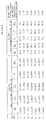
В табл. 1 представлен количественный состав раствора-расплава и полученного из него эпитаксиального слоя, согласно примерам 1-3, а также для промежуточных составов. In the table. 1 shows the quantitative composition of the melt solution and the epitaxial layer obtained from it, according to examples 1-3, as well as for intermediate compositions.
Спектральный диапазон оптических свойств слоев различного состава, полученных из растворов-расплавов, представлены в табл.2. Данные, отраженные в табл. показывают, что полученные слои полупроводникового материала позволяют расширить спектральный диапазон от 0,59 до 0,87 мкм. The spectral range of the optical properties of layers of various compositions obtained from solutions-melts are presented in table 2. The data reflected in the table. show that the obtained layers of semiconductor material can expand the spectral range from 0.59 to 0.87 microns.
Исследования состава эпитаксиального слоя AlxGayIn1-x-yPzAs1-z показали, что в случае подпитки его из кристалла-источника получались слои с однородным распределением компонентов по толщине от 5 до 96 мкм (см. табл. 2). Плотность дислокаций в таких слоях коррелирует с составом соответствующих трех- и четырехкомпонентных полупроводников (см. табл. 2). Рентгеноструктурные и люминесцентные исследования пятикомпонентных эпитаксиальных слоев показали улучшение структурного совершенства гетерограницы по сравнению с четырехкомпонентным твердым раствором (см. табл. 2 полуширина дифракционного максимума, механические напряжения, полуширина краевой полосы излучения).Studies of the composition of the Alx Gay In1-xy PzAs1-z epitaxial layer showed that in the case of feeding it from the source crystal, layers with a uniform distribution of components in thickness from 5 to 96 μm were obtained (see Table 2). The dislocation density in such layers correlates with the composition of the corresponding three- and four-component semiconductors (see Table 2). X-ray structural and luminescent studies of five-component epitaxial layers showed an improvement in the structural perfection of the heteroboundary as compared to a four-component solid solution (see Table 2, half-width of the diffraction maximum, mechanical stresses, half-width of the edge radiation band).
Claims (1)
Translated fromRussianPriority Applications (1)
| Application Number | Priority Date | Filing Date | Title |
|---|---|---|---|
| SU4944671RU2064541C1 (en) | 1991-04-08 | 1991-04-08 | Method of preparing heterostructures on the basis of semiconducting compounds a*991*991*991b*99v |
Applications Claiming Priority (1)
| Application Number | Priority Date | Filing Date | Title |
|---|---|---|---|
| SU4944671RU2064541C1 (en) | 1991-04-08 | 1991-04-08 | Method of preparing heterostructures on the basis of semiconducting compounds a*991*991*991b*99v |
Publications (1)
| Publication Number | Publication Date |
|---|---|
| RU2064541C1true RU2064541C1 (en) | 1996-07-27 |
Family
ID=21578877
Family Applications (1)
| Application Number | Title | Priority Date | Filing Date |
|---|---|---|---|
| SU4944671RU2064541C1 (en) | 1991-04-08 | 1991-04-08 | Method of preparing heterostructures on the basis of semiconducting compounds a*991*991*991b*99v |
Country Status (1)
| Country | Link |
|---|---|
| RU (1) | RU2064541C1 (en) |
- 1991
- 1991-04-08RUSU4944671patent/RU2064541C1/enactive
Non-Patent Citations (1)
| Title |
|---|
| 1. ЕПВ o 0229263, кл. С ЗО B 23/02, 1987. 2. Лозовский В.Н. и др. Особенности роста пятикомпонентных твердых растворов Al x Ga y In 1-x-y P 2 A 1-2 - арсенида галлия из раствора-расплава с подпиткой. 7-я Всес.конф. по росту кристаллов: Симп. по молекул.-луч.эпитаксии, 14-19 ноября 1988. Расш.тез. Т.2.- М.: 1988, с. 334 - 335.* |
Similar Documents
| Publication | Publication Date | Title |
|---|---|---|
| DE69738008T2 (en) | Semiconductor component | |
| US3802967A (en) | Iii-v compound on insulating substrate and its preparation and use | |
| US8029905B2 (en) | GeSiSn-based compounds, templates, and semiconductor structures | |
| DE69425328T2 (en) | CRYSTALLINE MULTI-LAYERED STRUCTURE AND METHOD FOR THE PRODUCTION THEREOF | |
| US5239188A (en) | Gallium nitride base semiconductor device | |
| DE69933169T2 (en) | Single crystal gallium nitride substrate and process for its preparation | |
| US4116733A (en) | Vapor phase growth technique of III-V compounds utilizing a preheating step | |
| US3933538A (en) | Method and apparatus for production of liquid phase epitaxial layers of semiconductors | |
| JPH0812844B2 (en) | (III) -Group V compound semiconductor and method for forming the same | |
| JP2001048698A (en) | Low resistance p-type single crystal zinc oxide and method for producing the same | |
| US4504329A (en) | Process for the epitaxial deposition of III-V compounds utilizing a binary alloy as the metallic source | |
| CA1134060A (en) | Epitaxial manufacture of a semiconductor device having a multi-layer structure | |
| Faurie et al. | New development on the control of homoepitaxial and heteroepitaxial growth of CdTe and HgCdTe by MBE | |
| RU2064541C1 (en) | Method of preparing heterostructures on the basis of semiconducting compounds a*991*991*991b*99v | |
| US3981764A (en) | III-V Compound semi-conductor crystal growth from a liquid phase on a substract including filtering liquid phase | |
| JPH0253097B2 (en) | ||
| US5204283A (en) | Method of growth II-VI semiconducting compounds | |
| US7550786B2 (en) | Compound semiconductor epitaxial substrate | |
| US4287527A (en) | Opto-electronic devices based on bulk crystals of complex semiconductors | |
| Uchida et al. | Extremely high Be doped Ga0. 47In0. 53As growth by chemical beam epitaxy | |
| Yang et al. | Compound Semiconductors | |
| Kukimoto | MOCVD—Current state and future | |
| JP2537296B2 (en) | <II>-<VI> Intergroup compound semiconductor device manufacturing method | |
| JPH0714785A (en) | Semiconductor epitaxial substrate and method for manufacturing the same | |
| JPH0526760B2 (en) |