RU2059026C1 - Scintillation material - Google Patents
Scintillation materialDownload PDFInfo
- Publication number
- RU2059026C1 RU2059026C1RU93026932/26ARU93026932ARU2059026C1RU 2059026 C1RU2059026 C1RU 2059026C1RU 93026932/26 ARU93026932/26 ARU 93026932/26ARU 93026932 ARU93026932 ARU 93026932ARU 2059026 C1RU2059026 C1RU 2059026C1
- Authority
- RU
- Russia
- Prior art keywords
- scintillation
- nabi
- crystals
- alkali metal
- scintillation material
- Prior art date
Links
- 239000000463materialSubstances0.000titleclaimsabstractdescription15
- 239000012535impuritySubstances0.000claimsabstractdescription13
- 229910052783alkali metalInorganic materials0.000claimsabstractdescription12
- 150000001340alkali metalsChemical class0.000claimsabstractdescription12
- 229910052792caesiumInorganic materials0.000claimsabstractdescription7
- 229910052701rubidiumInorganic materials0.000claimsabstract2
- PBYZMCDFOULPGH-UHFFFAOYSA-NtungstateChemical compound[O-][W]([O-])(=O)=OPBYZMCDFOULPGH-UHFFFAOYSA-N0.000claimsdescription4
- FSAJRXGMUISOIW-UHFFFAOYSA-Nbismuth sodiumChemical compound[Na].[Bi]FSAJRXGMUISOIW-UHFFFAOYSA-N0.000claimsdescription3
- 229910052744lithiumInorganic materials0.000abstractdescription6
- 229910052700potassiumInorganic materials0.000abstractdescription6
- 230000000694effectsEffects0.000abstractdescription2
- 239000000126substanceSubstances0.000abstractdescription2
- 239000013078crystalSubstances0.000description19
- 230000005855radiationEffects0.000description10
- 239000011734sodiumSubstances0.000description6
- 150000001768cationsChemical class0.000description5
- 229910052745leadInorganic materials0.000description5
- 238000000034methodMethods0.000description5
- 230000003287optical effectEffects0.000description5
- 239000000203mixtureSubstances0.000description4
- 230000005865ionizing radiationEffects0.000description3
- 239000002245particleSubstances0.000description3
- 238000006467substitution reactionMethods0.000description3
- 238000010521absorption reactionMethods0.000description2
- 150000001450anionsChemical class0.000description2
- 239000002019doping agentSubstances0.000description2
- 150000002500ionsChemical class0.000description2
- 238000004020luminiscence typeMethods0.000description2
- 239000011159matrix materialSubstances0.000description2
- 238000005259measurementMethods0.000description2
- 229910001415sodium ionInorganic materials0.000description2
- 238000004611spectroscopical analysisMethods0.000description2
- 238000001228spectrumMethods0.000description2
- 238000002834transmittanceMethods0.000description2
- 229910015902Bi 2 O 3Inorganic materials0.000description1
- DGAQECJNVWCQMB-PUAWFVPOSA-MIlexoside XXIXChemical compoundC[C@@H]1CC[C@@]2(CC[C@@]3(C(=CC[C@H]4[C@]3(CC[C@@H]5[C@@]4(CC[C@@H](C5(C)C)OS(=O)(=O)[O-])C)C)[C@@H]2[C@]1(C)O)C)C(=O)O[C@H]6[C@@H]([C@H]([C@@H]([C@H](O6)CO)O)O)O.[Na+]DGAQECJNVWCQMB-PUAWFVPOSA-M0.000description1
- 231100000987absorbed doseToxicity0.000description1
- 239000000654additiveSubstances0.000description1
- 150000001339alkali metal compoundsChemical class0.000description1
- 238000005275alloyingMethods0.000description1
- 238000004458analytical methodMethods0.000description1
- 125000000129anionic groupChemical group0.000description1
- 230000005540biological transmissionEffects0.000description1
- 229910052797bismuthInorganic materials0.000description1
- 229910052793cadmiumInorganic materials0.000description1
- BDOSMKKIYDKNTQ-UHFFFAOYSA-Ncadmium atomChemical compound[Cd]BDOSMKKIYDKNTQ-UHFFFAOYSA-N0.000description1
- 150000004649carbonic acid derivativesChemical class0.000description1
- 238000005336crackingMethods0.000description1
- 230000007547defectEffects0.000description1
- 238000001514detection methodMethods0.000description1
- 230000006866deteriorationEffects0.000description1
- 230000001788irregularEffects0.000description1
- 229910052751metalInorganic materials0.000description1
- 239000002184metalSubstances0.000description1
- 150000002739metalsChemical class0.000description1
- 230000001590oxidative effectEffects0.000description1
- 230000008092positive effectEffects0.000description1
- 238000001556precipitationMethods0.000description1
- 238000005395radioluminescenceMethods0.000description1
- 230000035945sensitivityEffects0.000description1
- 229910052708sodiumInorganic materials0.000description1
- 238000010561standard procedureMethods0.000description1
- 230000002123temporal effectEffects0.000description1
- 238000000411transmission spectrumMethods0.000description1
Images
Landscapes
- Measurement Of Radiation (AREA)
Abstract
Description
Translated fromRussianИзобретение относится к технике регистрации и спектрометрии ионизирующих излучений, в частности к сцинтилляционным материалам. The invention relates to techniques for recording and spectrometry of ionizing radiation, in particular to scintillation materials.
Известны сцинтилляционные кристаллы вольфраматов, в частности вольфрамата кадмия CdWO4(CWO) [1] Достоинствами CWO, как сцинтиллятора, являются большая плотность (7г, 9 г/см3), высокий эффективный атомный номер (Z 62), малая радиационная длина (1,10 см), значительный световой выход сцинтилляций (до 40% относительно NaT(Tl), достаточно большая длина волны максимума спектра излучения (λ= 480-540 нм), позволяющая использовать CWO как с фотоэлектронными умножителями, так и с фотодиодами.Known scintillation crystals of tungstates, in particular cadmium tungstate CdWO4 (CWO) [1] Advantages of CWO as a scintillator are high density (7 g, 9 g / cm3 ), high effective atomic number (Z 62), short radiation length (1 , 10 cm), a significant light output of scintillations (up to 40% relative to NaT (Tl), a sufficiently large wavelength of the maximum of the radiation spectrum (λ = 480-540 nm), which allows the use of CWO with both photoelectronic multipliers and photodiodes.
Недостатком CWO является значительное время высвечивания сцинтилляционного импульса, составляющее при комнатной температуре порядка 12000 нс (в импульсе присутствуют две компоненты с постоянными времени 5000 и 20000 нс). Кроме того, кристаллы CWO обладают невысокой радиационной стойкостью. Так, при облучении квантами средних энергий (Е 0,662 МэВ) снижение световыхода в зависимости от поглощенной дозы составляют 0,3% кГр. Эти факторы ограничивают применение сцинтиллятора CWO в устройствах детектирования ионизирующих излучений высоких энергий и трактах регистрации, требующих высокого временного разрешения. The disadvantage of CWO is the significant time of scintillation pulse emission, which is about 12000 ns at room temperature (two components with time constants of 5000 and 20,000 ns are present in the pulse). In addition, CWO crystals have low radiation resistance. So, when irradiated with medium-energy quanta (E 0.662 MeV), the decrease in light output depending on the absorbed dose is 0.3% kGy. These factors limit the use of the CWO scintillator in high energy ionizing radiation detection devices and recording paths requiring high time resolution.
Наиболее близким к изобретению является кристалл двойного вольфрамата натрия-висмута NaBi(WO4)2, используемый в радиаторах детекторов Черенкова [2]
Достоинства этого материала, как среды, преобразующей энергию ионизирующего излучения в кванты света, определяются его высокой плотностью (7,57 г/см3), большим эффективным атомным номером (Z71), малой радиационной длиной (1,01 см), высокой оптической прозрачностью в видимом и ультрафиолетовом (за исключением области 300-410 нм) диапазонах, быстродействием (порядка 3 нс) и значительной радиационной стойкостью снижение оптического пропускания происходит при дозах γ-облучения свыше 80 кГр и не превышает 0,15% кГр. Материал в качестве детекторов Черенкова находит применение для регистрации частиц высоких энергий. Как сцинтиллятор же кристалл NaBi(WO4)2 непригоден для детектирования γ-квантов, что определяется незначительным выходом света сцинтилляций, не превышающим при Еγ= 0,662 МэВ 0,2% относительно сцинтиллятора NaT(Tl).Closest to the invention is a sodium bismuth double tungstate crystal NaBi (WO4 )2 used in radiators of Cherenkov detectors [2]
The advantages of this material as a medium that converts the energy of ionizing radiation into light quanta are determined by its high density (7.57 g / cm3 ), large effective atomic number (Z71), small radiation length (1.01 cm), and high optical transparency in the visible and ultraviolet (with the exception of the region of 300-410 nm) ranges, speed (about 3 ns) and significant radiation resistance, a decrease in optical transmittance occurs at γ-radiation doses in excess of 80 kGy and does not exceed 0.15% kGy. The material as Cherenkov detectors is used to detect high-energy particles. As a scintillator, the NaBi (WO4 )2 crystal is unsuitable for detecting gamma quanta, which is determined by the insignificant scintillation light output not exceeding 0.2% at Eγ = 0.662 MeV relative to the NaT (Tl) scintillator.
Цель изобретения создание сцинтилляционного материала на основе двойного вольфрамата натрия-висмута, обладающего повышенным световым выходом сцинтилляций. The purpose of the invention is the creation of scintillation material based on double sodium tungstate-bismuth, which has an increased light output of scintillations.
Цель достигается тем, что кристалл NaBi(WO4)2 содержит дополнительно примесь щелочного металла из группы Li, K, Pb, Cs в количестве 0,005-0,3 мас.The goal is achieved in that the NaBi (WO4 )2 crystal additionally contains an alkali metal impurity from the group Li, K, Pb, Cs in an amount of 0.005-0.3 wt.
Выбор указанных щелочных металлов в качестве легирующей примеси обусловлен следующим. Известно, что сцинтиллирующие вольфраматы принадлежат к классу так называемых самоактивированных сцинтилляторов. Их радиолюминесценция обусловлена излучательным девозбуждением анионного комплекса WO


Монокристаллы сцинтиллятора NaBi(WO4):Me, где Ме берется из группы металлов Li, K, Pb, Cs, получают следующим образом. Исходную шихту составляют из смеси компонентов Na2CO3:B2O3:WO3 с добавкой соединения щелочного металла из указанной группы. Монокристаллы выращивают методом Чохральского в окислительной атмосфере в пластиновых тиглях при 935-980оС со скоростью вытягивания 2,0-5,0 мм/ч и скоростью вращения затравки 20-30 мин-1. По окончании процесса выращивания охлаждение кристаллов ведут со скоростью не более 50 К/ч.Single crystals of the NaBi scintillator (WO4 ): Me, where Me is taken from the group of metals Li, K, Pb, Cs, is prepared as follows. The initial charge is composed of a mixture of Na2 CO3 : B2 O3 : WO3 components with the addition of an alkali metal compound from the indicated group. Single crystals were grown by the Czochralski method in an oxidizing atmosphere plastinovyh crucibles atabout 935-980 C at a pulling rate of 2.0-5.0 mm / hour and rotation rate of the seed 20-30 min-1. At the end of the growing process, the crystals are cooled at a rate of not more than 50 K / h.
Полученные монокристаллы контролируют по содержанию примеси щелочного металла, по величине светового выхода сцинтилляций, времени высвечивания импульса и радиационной стойкости. При этом используют соответственно метод атомно-абсорбционного анализа, стандартную методику измерения световыхода по пику полного поглощения γ-квантов источника
137Cs, одноэлектронный метод при возбуждении α-частицами от источника
238Pu и измерение оптического пропускания образцов до и после γ-облучения фиксированной дозой от источника 60Со.The obtained single crystals are controlled by the content of alkali metal impurities, by the magnitude of the light output of scintillations, the time of emission of the pulse, and radiation resistance. In this case, the atomic absorption analysis method and the standard method for measuring the light yield from the peak of the total absorption of the γ-rays of the source are used respectively
137 Cs, single-electron method when excited by a-particles from a source
238 Pu and measurement of optical transmission of samples before and after γ-irradiation with a fixed dose from a source of 60Co.
П р и м е р ы. Исходную шихту готовили из смеси основных компонентов Na2CO3:Bi2O3:WO3. К навескам основной шихты вводили добавки щелочных металлов в виде карбонатов Ме2СО3, где Ме Li, K, Pb, Cs. Из составов методом Чохральского были выращены кристаллы NaBi(WO4)2:Me. Кристаллы, полученные в диапазоне содержаний примеси щелочных металлов до 0,3 мас. прозрачны, имеют желтую от слабой до средней интенсивности окраску, содержат малое количество визуально наблюдаемых дефектов (тонкодисперсных включений и микротрещин), локализованных в хвостовой зоне. Диаметр кристаллов составляет 20-23 мм, длина 60-80 мм. При содержании легирующей примеси 0,35 и более мас. присутствие включений и трещиноватость кристаллов резко возрастают, что связано с выпадением фаз, химически и структурно существенно отличающихся от матрицы. Такие образцы не прозрачны по всему объему.EXAMPLES The initial mixture was prepared from a mixture of the main components of Na2 CO3 : Bi2 O3 : WO3 . Alkali metal additives in the form of Me2 CO3 carbonates, where Me Li, K, Pb, Cs, were added to the bulk of the charge. From the compositions by the Czochralski method, NaBi (WO4 )2 : Me crystals were grown. Crystals obtained in the range of alkali metal impurity contents up to 0.3 wt. they are transparent, have a yellow to low to medium intensity color, contain a small number of visually observed defects (finely dispersed inclusions and microcracks) localized in the tail zone. The diameter of the crystals is 20-23 mm, length 60-80 mm. When the content of the dopant is 0.35 or more wt. the presence of inclusions and cracking of crystals increase sharply, which is associated with the precipitation of phases chemically and structurally significantly different from the matrix. Such samples are not transparent throughout.
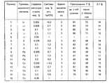
Для измерения сцинтилляционных характеристик из кристаллов изготавливали элементы диаметром 18 и толщиной 5 мм, торцы которых были полированы по классу Rz 0,025, а боковая поверхность матирована. Дополнительно отбирали пробы материала для контроля содержания легирующего щелочного металла. На изготовленных элементах контролировали также по оптическим спектрам пропускания радиационную стойкость материала. Спектры снимали на спектрофотометре на длине волны 480 нм до и после облучения элемента от источника γ-квантов с энергией 1,33 МэВ (60Со) дозами 12,0 Мрад. Результаты измерений содержания примеси, светового выхода сцинтилляций, времени высвечивания импульса и изменения оптического пропускания приведены в таблице.To measure scintillation characteristics, crystals were made of elements with a diameter of 18 and a thickness of 5 mm, the ends of which were polished according to the class Rz 0.025, and the side surface was frosted. Additionally, material samples were taken to control the alloying alkali metal content. On the manufactured elements, the radiation resistance of the material was also controlled by optical transmission spectra. The spectra were recorded on a spectrophotometer at a wavelength of 480 nm before and after irradiation of an element from a source of gamma rays with an energy of 1.33 MeV (60Co ) with doses of 12.0 Mrad. The results of measurements of the impurity content, scintillation light output, pulse luminescence time, and changes in optical transmittance are given in the table.
Из таблицы следует, что положительный эффект, достигнутый при введении в указанном количестве примесей щелочных металлов в кристаллы NaBi(WO4)2, состоит в том, что полученный сцинтилляционный материал обладает световыходом сцинтилляций, составляющим при оптимальном содержании примеси 0,1 мас. в случае добавки Li 2,1, K 1,65, Pb 1,0, Cs 0,8% относительно NaT(Tl), то есть соответственно в 10,5; 8,2; 5,0; 4,0 раза выше, чем у нелегированного кристалла. При этом введение примесей щелочных металлов в диапазоне концентраций 0,005-0,3 мас. не привело к ухудшению быстродействия и радиационной стойкости кристалла относительно материала, описанного в прототипе. Эффект повышения световыхода не обеспечивается при содержаниях примеси, меньших 0,005 и больших 0,3 мас. (примеры 1,5, 12 и 16 с введением примесей с минимальным (Li) и максимальным (Cs) ионными радиусами). В первом случае это связано с малой величиной замещения в кристаллической матрице ионов натрия на ионы примеси. Во втором обусловлено непрозрачностью кристалла, препятствующей выходу света сцинтилляций. Таким образом, диапазон концентраций примеси щелочного металла из группы Li, K, Pb, Cs, обеспечивающих достижение поставленной цели, составляет 0,005-0,3 мас.It follows from the table that the positive effect achieved by introducing alkali metals into the indicated amount of NaBi (WO4 )2 crystals consists in the fact that the obtained scintillation material has a scintillation light yield of 0.1 wt. in the case of the addition of Li 2.1, K 1.65, Pb 1.0, Cs 0.8% relative to NaT (Tl), that is, respectively, 10.5; 8.2; 5.0; 4.0 times higher than that of an undoped crystal. The introduction of impurities of alkali metals in the concentration range of 0.005-0.3 wt. did not lead to a deterioration in the speed and radiation resistance of the crystal relative to the material described in the prototype. The effect of increasing the light output is not provided when the impurity content is less than 0.005 and large 0.3 wt. (examples 1,5, 12 and 16 with the introduction of impurities with minimum (Li) and maximum (Cs) ionic radii). In the first case, this is due to the small amount of substitution in the crystalline matrix of sodium ions for impurity ions. The second is due to the opacity of the crystal, which prevents the exit of scintillation light. Thus, the range of concentrations of alkali metal impurities from the group of Li, K, Pb, Cs, ensuring the achievement of the goal, is 0.005-0.3 wt.
Полученный сцинтилляционный материал вследствие улучшения важной характеристики светового выхода сцинтилляций обладает большим относительно материала, описанного в прототипе, диапазоном применения. Сцинтилляционный кристалл может найти использование для регистрации спектрометрии частиц и квантов в устройствах физики высоких энергий, в частности в детекторах электромагнитных калориметров ускорителей на встречных пучках. В этом случае повышенный световыход обеспечит увеличение чувствительности регистрирующей системы, а малое время высвечивания и значительная радиационная стойкость обеспечат высокое временное разрешение и возможность работы в полях излучений большой интенсивности. The resulting scintillation material due to the improvement of an important characteristic of the light output of scintillations has a wide range of applications relative to the material described in the prototype. A scintillation crystal can be used for recording spectrometry of particles and quanta in high-energy physics devices, in particular, in detectors of electromagnetic calorimeters of oncoming beam accelerators. In this case, an increased light output will provide an increase in the sensitivity of the recording system, and a short exposure time and significant radiation resistance will provide a high temporal resolution and the ability to work in high-intensity radiation fields.
Claims (1)
Translated fromRussianPriority Applications (1)
| Application Number | Priority Date | Filing Date | Title |
|---|---|---|---|
| RU93026932/26ARU2059026C1 (en) | 1993-05-13 | 1993-05-13 | Scintillation material |
Applications Claiming Priority (1)
| Application Number | Priority Date | Filing Date | Title |
|---|---|---|---|
| RU93026932/26ARU2059026C1 (en) | 1993-05-13 | 1993-05-13 | Scintillation material |
Publications (2)
| Publication Number | Publication Date |
|---|---|
| RU93026932A RU93026932A (en) | 1996-03-10 |
| RU2059026C1true RU2059026C1 (en) | 1996-04-27 |
Family
ID=20141736
Family Applications (1)
| Application Number | Title | Priority Date | Filing Date |
|---|---|---|---|
| RU93026932/26ARU2059026C1 (en) | 1993-05-13 | 1993-05-13 | Scintillation material |
Country Status (1)
| Country | Link |
|---|---|
| RU (1) | RU2059026C1 (en) |
Cited By (4)
| Publication number | Priority date | Publication date | Assignee | Title |
|---|---|---|---|---|
| RU2132417C1 (en)* | 1998-01-22 | 1999-06-27 | Анненков Александр Николаевич | Method of preparing scintillation lead tungstate monocrystal |
| RU2145648C1 (en)* | 1997-04-22 | 2000-02-20 | Фурукава Ко., Лтд | Monocrystals of lead tungstate |
| RU2164562C1 (en)* | 2000-02-18 | 2001-03-27 | Аненков Александр Николаевич | Method of producing lead-tungstate scintillation single crystal |
| RU2485218C1 (en)* | 2012-03-29 | 2013-06-20 | Федеральное государственное бюджетное учреждение науки Институт физики твердого тела Российской академии наук (ИФТТ РАН) | Method for obtaining sodium tungstate-bismuth crystals |
- 1993
- 1993-05-13RURU93026932/26Apatent/RU2059026C1/ennot_activeIP Right Cessation
Non-Patent Citations (1)
| Title |
|---|
| 1. Цирлин Ю.А. и др. Оптимизация детектирования гамма-излучения сцинтилляционными кристаллами, М, Энергоатомиздат, 1991г, с.47-50. 2. Клевцов П.В. и др. Двойные молибдаты и вольфраматы щелочных металлов с висмутом M + Bi (TO 4 ) 2 . Кристаллография. 1973., т.18, вып.6, с.1192-1197.* |
Cited By (4)
| Publication number | Priority date | Publication date | Assignee | Title |
|---|---|---|---|---|
| RU2145648C1 (en)* | 1997-04-22 | 2000-02-20 | Фурукава Ко., Лтд | Monocrystals of lead tungstate |
| RU2132417C1 (en)* | 1998-01-22 | 1999-06-27 | Анненков Александр Николаевич | Method of preparing scintillation lead tungstate monocrystal |
| RU2164562C1 (en)* | 2000-02-18 | 2001-03-27 | Аненков Александр Николаевич | Method of producing lead-tungstate scintillation single crystal |
| RU2485218C1 (en)* | 2012-03-29 | 2013-06-20 | Федеральное государственное бюджетное учреждение науки Институт физики твердого тела Российской академии наук (ИФТТ РАН) | Method for obtaining sodium tungstate-bismuth crystals |
Similar Documents
| Publication | Publication Date | Title |
|---|---|---|
| Derenzo et al. | Prospects for new inorganic scintillators | |
| Zhu et al. | A study on the properties of lead tungstate crystals | |
| US5039858A (en) | Divalent fluoride doped cerium fluoride scintillator | |
| Farukhi et al. | Barium fluoride as a gamma ray and charged particle detector | |
| Rutstrom et al. | Improved light yield and growth of large-volume ultrafast single crystal scintillators Cs2ZnCl4 and Cs3ZnCl5 | |
| Belcher | The luminescence of irradiated transparent media and the Čerenkov effect-I. The luminescence of aqueous solutions of radioactive isotopes | |
| Kobayashi et al. | Radiation damage of BGO crystals due to low energy γ rays, high energy protons and fast neutrons | |
| Yanagida et al. | Phosphors for radiation detectors | |
| RU2596765C2 (en) | Scintillator, radiation detector and method for detecting radiation | |
| Moszynski | Energy resolution of scintillation detectors | |
| Kawaguchi et al. | Scintillation and Dosimetric Properties of Sn-doped ZnO-SiO2-B2O3 Glasses | |
| Kawaguchi et al. | Scintillation characteristics of Pr: CaF2 crystals for charged-particle detection | |
| Nakamura et al. | Non-doped Li2CO3 ceramics as a new radio-photoluminescence material | |
| RU2059026C1 (en) | Scintillation material | |
| Fujimoto et al. | Photoluminescence and radiation response properties of Ce3+-doped CsCaCl3 crystalline scintillator | |
| Usuda et al. | Phoswich detectors combining doubly or triply ZnS (Ag), NE102A, BGO and/or NaI (Tl) scintillators for simultaneous counting of α, β and γ rays | |
| Song et al. | Enhancement of alpha/beta ratio in NaI: Tl, 6Li neutron-gamma scintillators by rare earth co-doping | |
| Moses et al. | Lead carbonate, a new fast, heavy scintillator | |
| Shah et al. | RbGd/sub 2/Br/sub 7: Ce scintillators for gamma-ray and thermal neutron detection | |
| Okazaki et al. | Evaluation of optical and scintillation of Er: CaWO4 single crystals | |
| WO2012115234A1 (en) | Scintillator for neutron detection, and neutron radiation detector | |
| JPS63201095A (en) | Rare earth metal-aluminum-garnet base single crystal and manufacture | |
| Bhattacharya et al. | Codoped Lithium Sodium Iodide With Tl+ and Eu 2+ Activators for Neutron Detector | |
| CA2403066A1 (en) | Neutron scintillator | |
| Bergs et al. | Cyanoplatinate (II) salts as luminescent materials for scintillation counting |
Legal Events
| Date | Code | Title | Description |
|---|---|---|---|
| MM4A | The patent is invalid due to non-payment of fees | Effective date:20050514 |