KR960000792B1 - Burn-in Socket for Integrated Circuit Devices - Google Patents
Burn-in Socket for Integrated Circuit DevicesDownload PDFInfo
- Publication number
- KR960000792B1 KR960000792B1KR1019900001223AKR900001223AKR960000792B1KR 960000792 B1KR960000792 B1KR 960000792B1KR 1019900001223 AKR1019900001223 AKR 1019900001223AKR 900001223 AKR900001223 AKR 900001223AKR 960000792 B1KR960000792 B1KR 960000792B1
- Authority
- KR
- South Korea
- Prior art keywords
- socket
- contact
- integrated circuit
- cap
- package
- Prior art date
- Legal status (The legal status is an assumption and is not a legal conclusion. Google has not performed a legal analysis and makes no representation as to the accuracy of the status listed.)
- Expired - Fee Related
Links
Images


Classifications
- G—PHYSICS
- G01—MEASURING; TESTING
- G01R—MEASURING ELECTRIC VARIABLES; MEASURING MAGNETIC VARIABLES
- G01R31/00—Arrangements for testing electric properties; Arrangements for locating electric faults; Arrangements for electrical testing characterised by what is being tested not provided for elsewhere
- G01R31/26—Testing of individual semiconductor devices
- H—ELECTRICITY
- H01—ELECTRIC ELEMENTS
- H01R—ELECTRICALLY-CONDUCTIVE CONNECTIONS; STRUCTURAL ASSOCIATIONS OF A PLURALITY OF MUTUALLY-INSULATED ELECTRICAL CONNECTING ELEMENTS; COUPLING DEVICES; CURRENT COLLECTORS
- H01R13/00—Details of coupling devices of the kinds covered by groups H01R12/70 or H01R24/00 - H01R33/00
- H01R13/02—Contact members
- H01R13/193—Means for increasing contact pressure at the end of engagement of coupling part, e.g. zero insertion force or no friction
- G—PHYSICS
- G01—MEASURING; TESTING
- G01R—MEASURING ELECTRIC VARIABLES; MEASURING MAGNETIC VARIABLES
- G01R1/00—Details of instruments or arrangements of the types included in groups G01R5/00 - G01R13/00 and G01R31/00
- G01R1/02—General constructional details
- G01R1/04—Housings; Supporting members; Arrangements of terminals
- G01R1/0408—Test fixtures or contact fields; Connectors or connecting adaptors; Test clips; Test sockets
- G01R1/0433—Sockets for IC's or transistors
- H—ELECTRICITY
- H01—ELECTRIC ELEMENTS
- H01L—SEMICONDUCTOR DEVICES NOT COVERED BY CLASS H10
- H01L22/00—Testing or measuring during manufacture or treatment; Reliability measurements, i.e. testing of parts without further processing to modify the parts as such; Structural arrangements therefor
- H—ELECTRICITY
- H05—ELECTRIC TECHNIQUES NOT OTHERWISE PROVIDED FOR
- H05K—PRINTED CIRCUITS; CASINGS OR CONSTRUCTIONAL DETAILS OF ELECTRIC APPARATUS; MANUFACTURE OF ASSEMBLAGES OF ELECTRICAL COMPONENTS
- H05K7/00—Constructional details common to different types of electric apparatus
- H05K7/02—Arrangements of circuit components or wiring on supporting structure
- H05K7/10—Plug-in assemblages of components, e.g. IC sockets
- H05K7/1007—Plug-in assemblages of components, e.g. IC sockets with means for increasing contact pressure at the end of engagement of coupling parts
Landscapes
- Engineering & Computer Science (AREA)
- Microelectronics & Electronic Packaging (AREA)
- Computer Hardware Design (AREA)
- Physics & Mathematics (AREA)
- General Physics & Mathematics (AREA)
- Manufacturing & Machinery (AREA)
- Power Engineering (AREA)
- Testing Of Individual Semiconductor Devices (AREA)
- Connecting Device With Holders (AREA)
- Testing Or Measuring Of Semiconductors Or The Like (AREA)
Abstract
Translated fromKoreanDescription
Translated fromKorean제1도는 본 발명의 바람직한 실시예를 포함하는 소켓 위에 위치된 플라스틱 쿼드 플랫 팩(plastic quad flat pack) 패키지를 도시하는 분해 부분품 배열도.1 is an exploded part arrangement diagram showing a plastic quad flat pack package positioned over a socket comprising a preferred embodiment of the present invention.
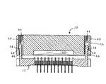
제2도는 PQFP 소켓의 단면도.2 is a cross-sectional view of a PQFP socket.
제3도는 소켓용으로 적합한 접촉단자들의 사시도.3 is a perspective view of contact terminals suitable for a socket.
제4도는 접촉단자들의 돌출부와 절연 하우징의 외부 레쥐(ledge)를 도시하는 부분 단면 사시도.4 is a partial cross-sectional perspective view showing the protrusions of the contact terminals and the outer ledge of the insulating housing.
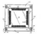
제5도는 본 발명의 바람직한 실시예를 포함하는 PQFP 소켓의 평면도.5 is a plan view of a PQFP socket incorporating a preferred embodiment of the present invention.
제6도는 캡이 절연 기부에 장착되는 방법을 도시하는, 제5도의 절단선 6-6을 따라 취한 단면도.FIG. 6 is a cross-sectional view taken along cut line 6-6 of FIG. 5 showing how the cap is mounted to the insulating base.
제7도는 내지 제10도는 소켓에 PQFP 패키지의 삽입과 접촉단자에 의한 걸윙(gullwing) 접촉 리이드 부의 맞물림을 나타내는 단면도.7 to 10 are cross-sectional views illustrating insertion of a PQFP package into a socket and engagement of a gullwing contact lead portion by a contact terminal.
본 발명은 집적회로 부품들로써 사용하기 위한 소켓에 관한 것이며, 특히 걸윙 리이드부가 있는 집적회로 부품들의 테스팅에 사용하기 위한 번-인(burn-in) 소켓에 관한 것이다.The present invention relates to a socket for use as integrated circuit components, and more particularly to a burn-in socket for use in testing integrated circuit components with a gullwing lead.
집적회로 부품들의 신뢰성을 보장하기 위해서는, 이들 부품들을 오랫동안 가속 열노화 테스팅하는 것이 필요하다. 이러한 번-인 테스팅은 때때로 모든 부품들에 대해서 실시되며, 그밖에 다른 경우에는 문제의 부품들이 만족스럽게 동작하는 것을 보장하기 위해서 통계적인 기준에 따라 실시된다.To ensure the reliability of integrated circuit components, it is necessary to accelerate thermal aging these components for a long time. This burn-in testing is sometimes performed on all parts, and in other cases, on a statistical basis to ensure that the parts in question work satisfactorily.
번-인 소켓들은 IC 칩들과 같은 집적회로 소자들을 테스트하기 위해서 사용되었다. 다수의 번-인 소켓은 집적회로 칩들 또는 칩 패키지들을 열노화 테스팅하기 위하여 번-인 오븐내에 위치된 프린트 회로기판 위에 배치될 수 있다. 번-인 소켓들은 리이드부 없는 세리믹 칩 캐리어들, 관통홀 리이드부가 있는 듀얼-인-라인 패키지들(DIP's) 및 리이드부가 있는 표면설치부품들로써 사용하기 위해 개발되었다.Burn-in sockets were used to test integrated circuit elements such as IC chips. Multiple burn-in sockets may be placed on a printed circuit board located in a burn-in oven for thermal aging testing integrated circuit chips or chip packages. Burn-in sockets have been developed for use as lead-free ceramic chip carriers, dual-in-line packages with through-hole leads (DIP's) and surface mount components with lead sections.
리이드부가 없는 칩 캐리어들의 테스팅에 사용하기 위한 하나의 번-인 소켓이 미국특허 4,491,377호에 나타나 있다. 그 소켓은 절연 기부를 통하여 연장하는 다수의 전기적 전도 핀들을 포함하는 절연 기부 지지체를 포함한다. 스프레더는 핀들에 관한 상호운동을 위해 설치된다. 스프레더가 핀들의 모서리와 맞닿는 경사면을 가짐에 따라, 절연 기부를 향한 스프레더의 운동은 핀들을 바깥쪽으로 이동시키게 된다. 리이드부가 없는 칩 캐리어는 핀들에 의하여 둘러싸여진 공간으로 삽입될 수 있다. 따라서, 핀들은 리이드부가 없는 칩 캐리어들 모서리 상의 홈들 내의 단자 영역과 접촉할 수 있다.One burn-in socket for use in testing chip carriers without leads is shown in US Pat. No. 4,491,377. The socket includes an insulating base support comprising a plurality of electrically conductive pins extending through the insulating base. Spreaders are installed for mutual movement with respect to the pins. As the spreader has a sloped surface that abuts the edges of the pins, the spreader's movement towards the insulating base causes the pins to move outward. The chip carrier without the lead portion can be inserted into the space surrounded by the pins. Thus, the pins may contact the terminal area in the grooves on the edge of the chip carriers without the lead portion.
미국특허 4,491,377호에 나타나 있는 무삽입력 소켓은 자동 삽입 장치로 사용될 때에 어떠한 장점들을 제공한다. 이 소켓에서 스프레더의 작동은 리이드부가 없는 칩 캐리어가 소켓으로 삽입되는 방향과 동일한 방향으로 직선운동하므로써 이루어질 수 있다. 개개의 칩 캐리어들은 삽입헤드에 위치될 수 있다. 삽입헤드는 칩 캐리어의 삽입을 위한 공간을 허용하기 위하여 단자 핀들을 이동시키는 소켓상의 스프레더와 접촉을 한다. 리이드부가 없는 칩 캐리어의 추출은 동일한 방법으로 이루어어질 수 있다. 미국특허 4,491,377호에 도시된 소켓이 플라스틱 직결 칩 캐리어 또는 리이드부가 없는 칩 캐리어들로 사용될때에, 이들 칩 캐리어들은 거꾸로 된 또는 “죽은 버그(bug)” 형태로 위치되어야 한다.The insertionless socket shown in US Pat. No. 4,491,377 offers certain advantages when used as an automatic insertion device. The operation of the spreader in this socket can be achieved by linear movement in the same direction as the chip carrier without the lead is inserted into the socket. Individual chip carriers may be located in the insertion head. The insertion head contacts the spreader on the socket that moves the terminal pins to allow space for insertion of the chip carrier. Extraction of the chip carrier without the lead portion can be made in the same way. When the sockets shown in US Pat. No. 4,491,377 are used as plastic direct chip carriers or chip carriers without lead portions, these chip carriers should be placed in an inverted or “dead” form.
그러나, 새로운 집적회로 패키지들의 출현은 번-인 테스팅 및 이에 사용되는 소켓들에 대해 추가적인 복잡성의 원인이 되었다. PQFP는 직사각형 또는 정사각형 플라스틱 몸체의 네 가장자리에 위치된 걸윙 리이드부를 갖는다. 이들 로우 프로파일 플라스틱 쿼드 플랫 패키지의 표준형은 0.025인치 중심선 간격의 걸윙리이드부를 갖는다. 이들 걸윙 리이드부는 PQFP 소자 몸체의 네 가장자리 모두로부터 연장한다. 걸윙 리이드부의 하부는 PQFP의 몸체의 하부표면 아래로 연장하는 발을 갖는다. 일반적으로, 이들 발은 수평위치에 대해 예를들면 0∼8°정도로 약간 경사져 있다.However, the emergence of new integrated circuit packages has caused additional complexity for burn-in testing and the sockets used therein. The PQFP has a gullwing lead located at four edges of a rectangular or square plastic body. Standard versions of these low profile plastic quad flat packages have gullwing leads with 0.025 inch centerline spacing. These gull wing leads extend from all four edges of the PQFP device body. The lower portion of the gullwing lead portion has a foot that extends below the lower surface of the body of the PQFP. In general, these feet are slightly inclined, for example, about 0 to 8 degrees with respect to the horizontal position.
사용시에, PQFP는 프린트 회로기판상의 표면설치패드에 납땜될 수 있다. 이들 이이드부들은 일반적으로 납땝 이음의 신뢰성을 증진시키기 위해 보편적인 방법으로 도금된다. 이들 도금된 리이드부의 하부표면은 번-인테스팅 동안에 손상되지 않는 것이 중요하다. 이들 걸윙 리이드부들은 비교적 작고 약하며, 번-인 테스팅 동안에 리이드부를 손상시키거나 지나친 압력이 가해지지 않도록 조심해야만 한다. 미국특허 4,491,377호에 도시된 형태의 소켓들은 PQFP 또는 쿼드 팩 부품들로써 사용하기에 적당하지 않다. 아답터가 리이드부를 지지하도록 PQFP에 아답터를 분리하여 부착하는 것이 가능하다. 이러한 형태의 아답터에 설치된 PQFP 패키지들은 미국특허 4,491,377호에 도시된 것과 같은 소켓에 삽입될 수 있다.In use, the PQFP can be soldered to a surface mount pad on a printed circuit board. These guide portions are generally plated in a universal manner to enhance the reliability of the brazed joints. It is important that the bottom surfaces of these plated lead portions are not damaged during burn-in testing. These gull wing leads are relatively small and weak, and care must be taken to avoid damaging or exerting excessive pressure during burn-in testing. Sockets of the type shown in US Pat. No. 4,491,377 are not suitable for use as PQFP or quad pack components. It is possible to detach and attach the adapter to the PQFP so that the adapter supports the lead portion. PQFP packages installed in this type of adapter may be inserted into sockets as shown in US Pat. No. 4,491,377.
그러나, 자동삽입장치에 관련하여 미국특허 4,491,377호에 도시된 형의 소켓을 사용하여 얻어지는 다른 능률은 만일 플라스틱 쿼드 플랫 패키지들은 아답터에 먼저 설치하는 것이 필요한 경우에는 감소되거나 제거된다. 그러나, 본 발명은 추가의 아답터가 필요없이 PQFP들과 같은 걸윙 패키지로 사용하기에 적당한 소켓을 포함한다.However, other efficiencies obtained using sockets of the type shown in US Pat. No. 4,491,377 with respect to the automatic insertion device are reduced or eliminated if plastic quad flat packages are required to be installed first in the adapter. However, the present invention includes a socket suitable for use in a gullwing package such as PQFPs without the need for additional adapters.
여기에서 설명된 소켓은 걸윙 리이드부를 갖는 플라스틱 쿼드 플랫 팩 패키지와 같은 전기적 부품의 전기적 상호접속을 이루기 위해 사용하는 것이다. 소켓은 절연 하우징으로부터 윗쪽으로 연장하는 다수의 접촉단자들을 갖는다. 절연 하우징에 대하여 이동할 수 있는 캡 또는 스프레더는 각 단자에 안쪽으로 압력을 가하기 위하여 접촉단자들고 맞물린다. 걸윙 부품은 아랫쪽으로 튀어나온 리이드부를 갖는 소켓에 “살아있는 버그” 형태로 삽입된다. 각 접촉단자의 상향 돌출부는 대응하는 걸윙 리이드부와 PQFP 패키지의 몸체 사이로 연장한다. 각 접촉단자들은 걸윙 리이드부의 발의 하부표면과 접촉하기 보다는 걸윙 리이드부들의 내부표면을 따라서 접촉을 한다. 리이드부가 표면설치프린트 회로기판 패드에 납땜되는 경우에 걸윙 리이드부들의 발의 손상을 피할 수 있다. 또한, 절연 하우징은 냉향 레쥐를 갖는다. 이 내향 레쥐는 대응하는 레쥐를 따라 연장하는 각 걸윙 리이드부의 자유단에 인접하도록 위치된다. 따라서 레쥐는 리이드부가 탄성 접촉단자들에 의해 외력을 받을때에 PQFP 걸윙 리이드부의 손상을 방지하는 정지장치로서 작용한다. 그러므로, 이 소켓은 지동 삽입장치로써 사용하기에 적당하며, 아답터의 추가등의 어떤 추가단계들을 필요로 하지 않는다.The sockets described herein are for use in making electrical interconnections of electrical components such as plastic quad flat pack packages with gullwing leads. The socket has a plurality of contact terminals extending upwards from the insulating housing. A cap or spreader that is movable relative to the insulated housing engages the contact terminals to inwardly press each terminal. The gullwing parts are inserted in the form of "live bugs" into sockets with protruding leads downwards. The upward projection of each contact terminal extends between the corresponding gull wing lead and the body of the PQFP package. Each contact terminal makes contact along the inner surface of the gull lead leads, rather than the bottom surface of the foot of the gull lead leads. When the lead portion is soldered to the surface mount printed circuit board pad, the damage of the foot of the gull lead lead portions can be avoided. The insulating housing also has a cold leg. This inward leg is positioned adjacent to the free end of each gull wing lead portion extending along the corresponding leg. Therefore, the leg acts as a stopper to prevent damage to the PQFP gull wing lead portion when the lead portion is subjected to external force by the elastic contact terminals. Therefore, this socket is suitable for use as a manual insertion device and does not require any additional steps such as the addition of an adapter.
본 발명은 지금부터 수반된 도면들에 의거한 실시예를 통하여 서술하기로 한다.The present invention will now be described through embodiments based on the accompanying drawings.
제1도는 집적회로 패키지 또는 리이드부가 있는 전자부품의 대표적인 것인 플라스틱 쿼드 플랫 패키지(2)를 도시한다. 플라스틱 퀴드 플랫 팩 패키지(2)는 집적회로 부품이 몸체(4)의 네 가장자리 각각으로부터 외부로 연장하는 걸윙 리이드부(6)를 갖는 플라스틱 몸체(4)내에 설치되어 있는 보편적인 집적회로 패키지를 나타낸다. 구석 연장부(8)는 일반적인 PQFP 패키지(2)의 몸체(4)의 각 구석에 위치되어 있다. 이들 구석 연장부(8)는 패키지(2)의 인접 가장자리에 줄지어 위치된 걸윙 접촉 리이드부(6)들 사이에 위치된다.FIG. 1 shows a plastic quad
본 발명의 바람직한 실시예를 포함하는 소켓(10)은 표준 PQFP 패키지(2)로써 사용하기에 특히 적합하다. 소켓(10)은 소켓 하우징(12)과 캡 스프레더(14)를 포함한다. 소켓 하우징(12)과 캡(14)은 번-인 테스팅 오븐에서의 온도들에 견딜 수 있는 일반적인 플라스틱 재료로 각각 제조된다. 절연 하우징(12)은 레쥐(20)와 소켓 기부(16) 사이에 일반적인 직각의 공간(18)을 형성하는 소켓 기부(16)로부터 위로 연장하는 다수의 레쥐(20)들과 중앙에 위치된 소켓 기부(16)를 갖는다.The
레쥐(20)들의 각각은 소켓 기부(16)의 상향 표면으로부터 바깥쪽으로 간격을 둔 공간(18)의 주변을 따라 위치된 내향 표면을 갖는다. 본 발명의 바람직한 실시예에서, 이 내향 표면은 수직표면부(24)로부터 기부(16)의 상부표면에 위치된 하부표면(28)까지 연장하는 약간의 경사진 계면(26)과 그의 상단에 인접한 수직부(24)를 갖는다. 벽(22)들은 기부(16)로부터 아랫쪽으로 연장하며, 다수의 포켓(30)들은 벽(22)들의 외부면을 따라 형성한다. 각 포켓(30)은 레쥐(20)들에 인접한 하부면(28)과 기부(16)의 상부표면 사이에 위치된 개구(38)를 갖는다. 다수의 리브(32)들은 일반적으로 개구(38)들 사이의 레쥐(20)들로부터 안쪽으로 연장한다. 하우징의 하부표면을 따라 위치된 하우징(12)의 일체부는 단자 설치부(34)를 제공한다. 각 포켓(30)은 접촉단자(40)들이 각각의 벽(22)의 외부를 포함하는 내부 포켓면(36)과 설치부(34) 사이을 연장하는 단자로서 각 포켓(30)들 내에 위치될 수 있도록 이 단자 설치부(34)로 연장하는 부분을 포함한다. 따라서, 포켓들은 각 포켓(30)이 레쥐(20)들과 소켓 기부(16)의 상부표면 사이에 형성된 공간(18)과 통하도록 기부(12)의 하부표면으로부터 개구(38)까지 위로 연장한다.Each of the
베릴륨동 합금과 같은 탄성 금속으로부터 엣지 스템프된 다수의 접촉단자(40)들은 각 포켓(30)내에 수용되도록 치수화된다. 각 접촉단자(40)는 위로 연장하는 접촉 코 또는 돌출부(42)를 갖는다. 이 돌출부(42)는 수직아암(46)의 상부 선단을 구성한다. 캠 종동부(44)는 아암(46)의 외부 모서리로부터 옆으로 연장한다. 아암(46)은 본 발명의 실시예에서 아암(46)의 폭보다 더 작은 폭을 갖는 곡부를 포함하는 비교적 큰 탄성력의 스프링부에 연결된다. 탄성 스프링부(48)는 접촉 기부(50)의 내부와 그의 하단에서 합체된다.
접촉 기부(50)는 접촉단자 아암(46)의 내부 모서리를 지나 안쪽으로, 그리고 캠 종동부(44)의 외부 선단을 지나 바깥쪽으로 돌출한다. 접촉 기부(50)는 일반적으로 수평으로 연장한다. 접촉 기둥(52)들은 접촉 기부(50)의 하부 모서리로부터 아래쪽으로 연장한다.The
본 발명의 바람직한 실시예에서는, 세 개의 각기 다른 접촉 기부 형태가 사용되고 있다. 단지 세 개의 다른 접촉단자들 사이의 차이는 각 접촉기둥(52)의 위치에 있다. 인접한 접촉단자(40)들 상의 접촉기둥 위치를 오프셋팅 또는 스태거링(staggering)하므로써, 좀더 가까운 접촉간격이 프린트 회로기판 상에 얻어질 수 있다. 접촉기둥(52)들의 스태거링은 번-인 소켓이 부착되는 프린트 회로기판 상에 트레이스(trace)들의 간격을 가깝게 하는 것이 요구된다. 외부 탭부(54)는 접촉 기부(50)로부터 위로 연장한다. 분명히 알 수 있는 바와 같이, 외부 탭(54)을 갖는 수평 연장 접촉기부는 접촉단자들이 절연 하우징의 하부에 삽입될 수 있도록 절연 하우징(12)에 접촉단자(40)들을 장착하기 위한 수단을 제공한다.In a preferred embodiment of the invention, three different contact base forms are used. The difference between only three different contact terminals is at the position of each
캡(14)은 캡(14)의 구석들에 위치된 구멍(64)들을 통하여 절연 하우징(12)으로부터 위로 연장하는 래치아암(66)들에 의하여 절연 하우징(12)에 장착된다.The
캡(14)은 공간(18)으로 정렬된 개구를 둘러싸는 4측벽(60)을 갖는 골조부재를 포함한다. 구멍(64)들은 인접한 벽(60)이 교차하는 구석들에 위치되어 있다. 래치아암(66)은 그의 상단 근처에 위치된 하향 래칭 숄더(58)를 갖는다. 상향 래칭 숄더(68)는 각 구멍(64)의 내부에 위치되어 있다. 캡(14)은 래치아암(66)들을 구멍(64)에 삽입하므로써 절연 하우징(12)에 장착될 수 있다. 각 래치아암(64)의 상부 외면 모서리의 경사면은 하향 숄더(58)가 상향 숄더(68) 위에 위치되는 점으로 래치아암이 용이하게 삽입될 수 있도록 래치아암(66)을 안으로 이동할 수 있다. 래치아암(66)은 숄더(58,68)들이 캡(14)을 절연 하우징(12) 위에 고착시키는 작용을 하도록 이 점에서 그들의 최외각 위치로 될 것이다.The
접촉단자(40)들은 캡(14)이 절연 하우징에 장착되기 전후, 언제라도 절연 하우징(12)으로 삽입될 수 있다. 전술된 바와 같이, 접촉단자(40)들은 절연 하우징(12)의 밑바닥으로부터 각 포켓(30)들로 삽입된다.The
각 포켓(30)은 단자아암(46)과 비교적 큰 탄성부(48)들을 수용하기에 충분한 공간을 갖는다. 접촉 기부와 그의 외부 끝에 있는 연장부(54)는 접촉단자 기부(50)가 이들 홈에 고정되고 각 단자(40)들이 대응 포켓(30)내에 보유되도록 각 포켓(30)의 하향 홈들에 꼭 끼워진다. 아암(46)의 상단에 위치된 접촉 코 또는 돌출부는 포켓(30)이 상단에 있는 개구(38)를 통하여 돌출한다. 각 돌출부(42)는 거의 인접한 래쥐(20)의 계면으로부터 간격을 두고 있는 돌출부(42)로서 인접 리브(32)들 사이에 배열된다. 각 개구(38)는 접촉단자가 구부러질때에 접촉 돌출부(42)가 개구(38) 안으로 이동되도록 돌출부(42)의 폭보다 더 길다. 캠 종동부(44)는 바깥쪽으로 연장하며, 캡(14)의 벽(60)의 내하부면 상의 하향 경사면(62)과 맞닿는다. 이 경사면(62)은 공간(18)의 각 변을 따라 위치된 각 접촉 단자(40)의 캠 종동면(44)의 외부 반경부와 접촉을 유지한다. 접촉단자(40)들은 줄지어 위치되어 있기 때문에, 단일 캠밍(camming) 표면(62)은 다수의 접촉단자들 상의 캠밍 아암(44)과 맞닿을 것이다. 캡(14)의 하향운동은 내부의 경사진 캠밍 표면(62)과 단자(40)들 사이의 상대적 운동을 일으킬 것이다. 캠 종동부재(44)를 통하여 단자들에 전달되는 이 상대적 운동은 제7도 내지 제10도의 사시도에서 볼 때, 각 단자(40)를 내부 또는 시계방향으로 기울어지게 할 것이다.Each
걸윙 PQFP 패키지의 삽입이 제7도 내지 제10도에 나타나 있다. 제7도는 걸윙 패키지 삽입 바로 전의 소켓(10)의 중립 위치를 도시한다. 패키지(4)는 패키지(4)가 소켓 위에 위치된 공간(18) 내에 삽입될 수 있도록 대응 접촉단자(40)와 제휴된 리이드부(6)와 더불어 도시되어 있다. 패키지(4)는 또한 캡의 외벽(60)사이에 삽입될 수 있도록 위치되어 있다.Insertion of the Gullwing PQFP package is shown in FIGS. 7 shows the neutral position of the
제8도는 패키지(4)를 삽입력 없이 삽입하기 위한 첫 번째 단계가 캡(14)에 전달되는 하향력을 필요로 하는 것을 도시한다. 캠밍 표면(62)은, 접촉 코 또는 돌출부(42)가 안쪽으로 기울어지도록 캠 종동부재(44)와 맞닿는다. 접촉 돌출부(42)는 걸윙 리이드부(6)의 발 부분이 레쥐(26)와 접촉 돌출부(42) 사이로 삽입되기에 충분히 안쪽으로 기울어질 수 있음을 유의하여야 한다.FIG. 8 shows that the first step for inserting the
제9도는 레쥐(20)의 내면(26)과 인접하게 위치되고 이에 마주보는 발 6a의 외부 선단과 함께 걸윙 리이드부(6)의 발 6a가 안으로 기울어진 접촉 돌출부(42)를 지나 바깥쪽으로 놓여진 위치로 삽입된 PQFP 패키지(2)를 도시한다. 접촉 발 6a는 레쥐(20)의 하부면(28) 위에 있도록 위치된다. 캡(14)에 가해진 하향력의 제거는 접촉 캠(46)을 바깥쪽으로 기울어지게 하여, 돌출부(42)가 걸윙 리이드부(6)와 PQFP(2)의 몸체(4)사이의 걸윙 리이드부(6)의 내부면과 맞닿는다. 걸윙 리이드부(6)의 외부 선단이 레쥐(20)의 내부면(26)과 접촉하기 때문에 각 걸윙 리이드부(6)는 스프링 작동 접촉 코(42)의 맞닿음에 의하여 지나친 압력이 가해지지 않을 것이다. 더욱이, 접촉단자(40)는 걸윙 접촉 리이드부(6)의 표면과 맞물리지 않기 때문에 프린트 회로 기판상의 표면설치 패드와의 양호한 납땜이음 형성은 신뢰할 수 있다.FIG. 9 is located adjacent to the
PQFP 패키지의 추출은 제7도 내지 제10도의 단계들을 반대로 함으로써 간단히 이루어질 수 있다. 캡(14)에 하향력을 인가하면 패키지(2)가 추출될 수 있도록 접촉 단자(40)들로부터 걸윙 리이드부(6)가 다시 풀린다. 제7∼10도에 도시된 바와 같이, 이 소켓 형태는 단지 직선운동에 의해서만으로 작동될 수 있으며, 패키지(2)들은 직선운동에 의하여 소켓(2) 위의 공간(18)으로 삽입될 수 있다. 따라서, 이 소켓은 자동 삽입 및 자동 추출 장치로 사용될 수 있다. 더욱이, 리이드부들의 손상을 방지하기 위하여 PQFP 패키지(2)에 아답터가 부착되지 않아도 된다. 비록 본 발명의 바람직한 실시예가 걸윙 리이드부들을 갖는 플라스틱 쿼드 플랫 팩 패키지들로 사용하기 위한 번-인 소켓에 대해 실시되었지만, 본 발명은 또한 PQFP 패키지들에 사용된 형태의 약한 걸윙 리이드부들을 갖는 어떤 다른 부품에도 응용될 수 있다는 것을 알아야 한다. 그러므로, 본 발명은 여기에 나타난 바람직한 실시예로만 제한되지 않는다.Extraction of the PQFP package can be accomplished simply by reversing the steps of FIGS. Applying a downward force to the
Claims (1)
Translated fromKoreanApplications Claiming Priority (3)
| Application Number | Priority Date | Filing Date | Title |
|---|---|---|---|
| US07/310,254 | 1989-02-13 | ||
| US07/310,254US4919623A (en) | 1989-02-13 | 1989-02-13 | Burn-in socket for integrated circuit device |
| US07/310254 | 1989-02-13 |
Publications (2)
| Publication Number | Publication Date |
|---|---|
| KR900013611A KR900013611A (en) | 1990-09-06 |
| KR960000792B1true KR960000792B1 (en) | 1996-01-12 |
Family
ID=23201660
Family Applications (1)
| Application Number | Title | Priority Date | Filing Date |
|---|---|---|---|
| KR1019900001223AExpired - Fee RelatedKR960000792B1 (en) | 1989-02-13 | 1990-02-02 | Burn-in Socket for Integrated Circuit Devices |
Country Status (4)
| Country | Link |
|---|---|
| US (1) | US4919623A (en) |
| JP (1) | JPH02266276A (en) |
| KR (1) | KR960000792B1 (en) |
| GB (1) | GB2229051B (en) |
Families Citing this family (14)
| Publication number | Priority date | Publication date | Assignee | Title |
|---|---|---|---|---|
| US5373230A (en)* | 1991-06-17 | 1994-12-13 | Itt Corporation | Test clip for five pitch IC |
| US5154620A (en)* | 1991-08-09 | 1992-10-13 | Molex Incorporated | Chip carrier socket assembly |
| US5205741A (en)* | 1991-08-14 | 1993-04-27 | Hewlett-Packard Company | Connector assembly for testing integrated circuit packages |
| US5373420A (en)* | 1993-03-19 | 1994-12-13 | Kun Yen Electronic Co., Ltd. | Chip carrier for fastening a chip to a printed circuit board |
| US7579269B2 (en)* | 1993-11-16 | 2009-08-25 | Formfactor, Inc. | Microelectronic spring contact elements |
| US6727580B1 (en)* | 1993-11-16 | 2004-04-27 | Formfactor, Inc. | Microelectronic spring contact elements |
| JPH11111416A (en)* | 1997-09-05 | 1999-04-23 | Molex Inc | Ic socket |
| KR20010046031A (en)* | 1999-11-10 | 2001-06-05 | 송재인 | An ic socket structure |
| US6499215B1 (en)* | 2000-06-29 | 2002-12-31 | International Business Machines Corporation | Processing of circuit boards with protective, adhesive-less covers on area array bonding sites |
| US20050128726A1 (en)* | 2003-12-10 | 2005-06-16 | Thompson Jill H. | System and method for protecting pins of an integrated circuit |
| TWM279071U (en)* | 2005-02-25 | 2005-10-21 | Hon Hai Prec Ind Co Ltd | Electrical connector |
| JP2019125438A (en)* | 2018-01-12 | 2019-07-25 | 東芝メモリ株式会社 | IC socket |
| DE102018106455B4 (en)* | 2018-03-20 | 2020-03-26 | Ie Assets Gmbh & Co. Kg | Fan wheel to be driven in one direction of rotation |
| KR102248916B1 (en)* | 2020-04-10 | 2021-05-07 | 주식회사 오킨스전자 | Test socket |
Family Cites Families (40)
| Publication number | Priority date | Publication date | Assignee | Title |
|---|---|---|---|---|
| US2992401A (en)* | 1957-11-06 | 1961-07-11 | Frank Adam Electric Co | Plug-in busduct |
| GB1152765A (en)* | 1967-01-24 | 1969-05-21 | Amp Inc | An Electrical Circuit Assembly |
| US3683317A (en)* | 1970-07-20 | 1972-08-08 | Cambridge Thermionic Corp | Minimal insertion force connector |
| BE789688A (en)* | 1971-10-06 | 1973-04-04 | Amp Inc | CONNECTOR |
| GB1405417A (en)* | 1971-11-19 | 1975-09-10 | Carr Fastener Co Ltd | Electrical connection sockets |
| US3848221A (en)* | 1973-03-07 | 1974-11-12 | Int Prod Technology Corp | Contact assembly utilizing flexible contacts for pins of integrated circuits |
| US3883207A (en)* | 1973-09-13 | 1975-05-13 | Molex Inc | Low insertion force connector for modular circuit packages |
| US4052117A (en)* | 1975-10-20 | 1977-10-04 | A P Products Incorporated | Integrated circuit socket |
| US4080032A (en)* | 1976-09-03 | 1978-03-21 | Amp Incorporated | Zero insertion force connector |
| US4159861A (en)* | 1977-12-30 | 1979-07-03 | International Telephone And Telegraph Corporation | Zero insertion force connector |
| US4331371A (en)* | 1979-03-09 | 1982-05-25 | Japan Aviation Electronics Industry, Ltd. | Electrical connector |
| US4312555A (en)* | 1979-10-17 | 1982-01-26 | Thomas & Betts Corporation | Receptacle for stacking electronic packages |
| US4266840A (en)* | 1979-10-29 | 1981-05-12 | Jack Seidler | Circuit holder |
| US4343524A (en)* | 1980-06-30 | 1982-08-10 | Amp Incorporated | Zero insertion force connector |
| US4391408A (en)* | 1980-09-05 | 1983-07-05 | Augat Inc. | Low insertion force connector |
| US4350402A (en)* | 1980-09-17 | 1982-09-21 | Amp Incorporated | Board mount zero insertion force connector |
| US4381130A (en)* | 1980-09-29 | 1983-04-26 | Burroughs Corporation | Zero insertion force connector for integrated circuit packages |
| US4349238A (en)* | 1980-11-05 | 1982-09-14 | Amp Incorporated | Integrated circuit package connector |
| US4422703A (en)* | 1981-09-15 | 1983-12-27 | Thomas & Betts Corporation | Electrical connector for use with multi-pin arrays |
| DE3242606A1 (en)* | 1982-02-15 | 1983-08-25 | Itw-Ateco Gmbh, 2000 Norderstedt | CLOTHES FOR SPORTSHOES, ESPECIALLY FOOTBALL SHOES |
| US4491377A (en)* | 1982-04-19 | 1985-01-01 | Pfaff Wayne | Mounting housing for leadless chip carrier |
| US4509812A (en)* | 1982-04-21 | 1985-04-09 | Karl Lotter | Plug connector for dil components |
| US4461525A (en)* | 1982-08-17 | 1984-07-24 | Wells Electronics, Inc. | Integrated circuit test socket |
| US4470650A (en)* | 1982-12-13 | 1984-09-11 | Amp Incorporated | Dual-in-line plug and socket assemblies |
| EP0404277B1 (en)* | 1984-02-27 | 1994-09-28 | The Whitaker Corporation | Method of inserting a chip carrier contact into a housing |
| US4533192A (en)* | 1984-04-25 | 1985-08-06 | Minnesota Mining And Manufacturing Company | Integrated circuit test socket |
| US4547031A (en)* | 1984-06-29 | 1985-10-15 | Amp Incorporated | Chip carrier socket and contact |
| US4630875A (en)* | 1984-07-02 | 1986-12-23 | Amp Incorporated | Chip carrier socket which requires low insertion force for the chip carrier |
| US4718855A (en)* | 1984-12-03 | 1988-01-12 | Amp Incorporated | Socket for integrated circuit component |
| US4623208A (en)* | 1985-04-03 | 1986-11-18 | Wells Electronic, Inc. | Leadless chip carrier socket |
| US4808119A (en)* | 1985-08-30 | 1989-02-28 | Pfaff Wayne | Zero insertion force mounting housings for electronic device packages |
| JPS6293964A (en)* | 1985-10-21 | 1987-04-30 | Dai Ichi Seiko Co Ltd | Ic testing socket |
| US4669796A (en)* | 1985-11-22 | 1987-06-02 | Wells Electronics, Inc. | RAM connector |
| US4799897A (en)* | 1985-12-30 | 1989-01-24 | Dai-Ichi Seiko Kabushiki Kaisha | IC tester socket |
| JPS62160676A (en)* | 1985-12-31 | 1987-07-16 | 日本テキサス・インスツルメンツ株式会社 | socket |
| US4678255A (en)* | 1986-04-03 | 1987-07-07 | Wells Electronics, Inc. | Chip connector |
| JPH0218547Y2 (en)* | 1986-05-02 | 1990-05-23 | ||
| JP2784570B2 (en)* | 1987-06-09 | 1998-08-06 | 日本テキサス・インスツルメンツ 株式会社 | Socket |
| US4750890A (en)* | 1987-06-18 | 1988-06-14 | The J. M. Ney Company | Test socket for an integrated circuit package |
| US4824389A (en)* | 1988-04-26 | 1989-04-25 | Precision Connector Designs, Inc. | Socket for electronic component |
- 1989
- 1989-02-13USUS07/310,254patent/US4919623A/ennot_activeExpired - Fee Related
- 1990
- 1990-01-29JPJP2018795Apatent/JPH02266276A/enactivePending
- 1990-02-02KRKR1019900001223Apatent/KR960000792B1/ennot_activeExpired - Fee Related
- 1990-02-02GBGB9002380Apatent/GB2229051B/ennot_activeExpired - Fee Related
Also Published As
| Publication number | Publication date |
|---|---|
| JPH02266276A (en) | 1990-10-31 |
| GB2229051B (en) | 1993-10-06 |
| KR900013611A (en) | 1990-09-06 |
| GB2229051A (en) | 1990-09-12 |
| US4919623A (en) | 1990-04-24 |
| GB9002380D0 (en) | 1990-04-04 |
Similar Documents
| Publication | Publication Date | Title |
|---|---|---|
| US6113399A (en) | Low-profile socketed packaging system with land-grid array and thermally conductive slug | |
| US3940786A (en) | Device for connecting leadless integrated circuit package to a printed circuit board | |
| KR960000792B1 (en) | Burn-in Socket for Integrated Circuit Devices | |
| US4652973A (en) | Chip carrier mounting apparatus | |
| US3989331A (en) | Dual-in-line socket | |
| US3883207A (en) | Low insertion force connector for modular circuit packages | |
| US4018494A (en) | Interconnection for electrically connecting two vertically stacked electronic packages | |
| KR20040024458A (en) | Lga socket contact | |
| US4954088A (en) | Socket for mounting an IC chip package on a printed circuit board | |
| US7654862B2 (en) | IC package having improved structure | |
| US6755668B2 (en) | Surface mounted socket assembly | |
| US5006962A (en) | Apparatus for surface mounting an integrated circuit package | |
| US5318451A (en) | Stackable interconnection socket | |
| JPH0789507B2 (en) | Chip carrier socket assembly | |
| JPH09266021A (en) | Socket for electric part | |
| JPH08512168A (en) | High-density electronic device connector | |
| JP2002071750A (en) | Carrier and pusher for handler device and handler device | |
| KR100279793B1 (en) | Socket for electrical parts | |
| KR950008234B1 (en) | Leadless chip carrier socket | |
| KR100318621B1 (en) | IC Device Test Socket Using Symmetrically structured Contact Pin | |
| JPH10255939A (en) | Socket for electric component | |
| JP3463872B2 (en) | Socket for electrical components | |
| JP3255387B2 (en) | IC socket | |
| JP2002190361A (en) | Socket for electrical component | |
| KR910006780Y1 (en) | Pin Test Socket for LCC Type Components |
Legal Events
| Date | Code | Title | Description |
|---|---|---|---|
| PA0109 | Patent application | St.27 status event code:A-0-1-A10-A12-nap-PA0109 | |
| R17-X000 | Change to representative recorded | St.27 status event code:A-3-3-R10-R17-oth-X000 | |
| PG1501 | Laying open of application | St.27 status event code:A-1-1-Q10-Q12-nap-PG1501 | |
| A201 | Request for examination | ||
| PA0201 | Request for examination | St.27 status event code:A-1-2-D10-D11-exm-PA0201 | |
| G160 | Decision to publish patent application | ||
| PG1605 | Publication of application before grant of patent | St.27 status event code:A-2-2-Q10-Q13-nap-PG1605 | |
| E701 | Decision to grant or registration of patent right | ||
| PE0701 | Decision of registration | St.27 status event code:A-1-2-D10-D22-exm-PE0701 | |
| GRNT | Written decision to grant | ||
| PR0701 | Registration of establishment | St.27 status event code:A-2-4-F10-F11-exm-PR0701 | |
| PR1002 | Payment of registration fee | St.27 status event code:A-2-2-U10-U11-oth-PR1002 Fee payment year number:1 | |
| PR1001 | Payment of annual fee | St.27 status event code:A-4-4-U10-U11-oth-PR1001 Fee payment year number:4 | |
| FPAY | Annual fee payment | Payment date:19991222 Year of fee payment:5 | |
| PR1001 | Payment of annual fee | St.27 status event code:A-4-4-U10-U11-oth-PR1001 Fee payment year number:5 | |
| LAPS | Lapse due to unpaid annual fee | ||
| PC1903 | Unpaid annual fee | St.27 status event code:A-4-4-U10-U13-oth-PC1903 Not in force date:20010113 Payment event data comment text:Termination Category : DEFAULT_OF_REGISTRATION_FEE | |
| PC1903 | Unpaid annual fee | St.27 status event code:N-4-6-H10-H13-oth-PC1903 Ip right cessation event data comment text:Termination Category : DEFAULT_OF_REGISTRATION_FEE Not in force date:20010113 | |
| P22-X000 | Classification modified | St.27 status event code:A-4-4-P10-P22-nap-X000 |