KR950014277B1 - Heterojunction Bipolar Transistors - Google Patents
Heterojunction Bipolar TransistorsDownload PDFInfo
- Publication number
- KR950014277B1 KR950014277B1KR1019870010563AKR870010563AKR950014277B1KR 950014277 B1KR950014277 B1KR 950014277B1KR 1019870010563 AKR1019870010563 AKR 1019870010563AKR 870010563 AKR870010563 AKR 870010563AKR 950014277 B1KR950014277 B1KR 950014277B1
- Authority
- KR
- South Korea
- Prior art keywords
- region
- emitter
- collector
- layer
- heterojunction bipolar
- Prior art date
- Legal status (The legal status is an assumption and is not a legal conclusion. Google has not performed a legal analysis and makes no representation as to the accuracy of the status listed.)
- Expired - Fee Related
Links
Images


Classifications
- H—ELECTRICITY
- H10—SEMICONDUCTOR DEVICES; ELECTRIC SOLID-STATE DEVICES NOT OTHERWISE PROVIDED FOR
- H10D—INORGANIC ELECTRIC SEMICONDUCTOR DEVICES
- H10D10/00—Bipolar junction transistors [BJT]
- H10D10/80—Heterojunction BJTs
- H10D10/821—Vertical heterojunction BJTs
Landscapes
- Bipolar Transistors (AREA)
Abstract
Translated fromKoreanDescription
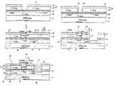
Translated fromKorean제1도 a-e는 본원 발명에 의한 헤테로 접합형 바이폴러 트랜지스터의 일실시예를 나타낸 제조공정도.1 is a manufacturing process diagram showing an embodiment of a heterojunction bipolar transistor according to the present invention.
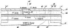
제2도는 본원 발명의 다른 실시예를 나타낸 단면도.2 is a cross-sectional view showing another embodiment of the present invention.
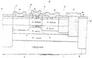
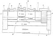
제3도 및 제4도는 각기 종래의 헤테로접합형 바이폴러 트랜지스터의 예를 나타낸 단면도.3 and 4 are cross-sectional views each showing an example of a conventional heterojunction bipolar transistor.
* 도면의 주요 부분에 대한 부호의 설명* Explanation of symbols for the main parts of the drawings
31 : 반절연성, GaAs기판 32 : 에미터전극취출층31: semi-insulating, GaAs substrate 32: emitter electrode extraction layer
33 : 에미터영역 34 : P-AlGaAs의 블록층33: emitter region 34: block layer of P-AlGaAs
35 : P+-GaAs 층 36 : 외부 베이스영역35: P + -GaAs layer 36: outer base region
40 : 베이스영역 41 : 콜렉터 영역40: base area 41: collector area
42 : 갭층42: gap layer
본원 발명은 헤테로접합형 바이폴러트랜지스터에 관한 것이다.The present invention relates to a heterojunction bipolar transistor.
본원 발명은 헤테로접합형 바이폴러트랜지스터에 있어서, 진성(眞性) 베이스영역과 외부 베이스영역과의 경계에 헤테로접합을 가짐으로써 페리퍼리(periphery) 효과를 없애고, 높은 전류증폭율을 얻도록 한 것이다.In the heterojunction bipolar transistor, the present invention has a heterojunction at the boundary between the intrinsic base region and the external base region to eliminate the peripheral effect and to obtain a high current amplification factor. .
헤테로접합형 바이폴러트랜지스터는 실리콘 등에 의한 호모접합형 바이폴러트랜지스터가 갖는 결점을 극복할 수 있는 트랜지스터이다. 즉 에미터(E)에 AlGaAs를, 베이스(B) 및 콜레겉(C)에 GaAs를 사용한 경우의 헤테로접합형 바이폴러트랜지스터를 예로 들면, 베이스중의 다수 캐리어인 정공(正孔)은 E-B 간의 밴드감차(△Eg)의 에너지장벽때문에 에미터중에 확산할 수 없으며, 베이스전류는 감소하고, 에미터에서 베이스에의 전자(電子)의 주입효율이 증가한다. 따라서 베이스농도를 크게하고 에미터농도를 작게하여도 증폭도(β=IC/IB)를 크게할 수 있다. 이것은 고속성에 관계되는 베이스저항과 E-B간 접합용량을 작게 할 수있는 것을 의미하고, 실리콘 바이폴러트랜지스터보다 고속이라는 것을 이론적으로나 실험적으로도 나타내는 것이다.The heterojunction bipolar transistor is a transistor that can overcome the drawbacks of the homojunction bipolar transistor by silicon or the like. In other words, in the case where AlGaAs is used as the emitter (E) and GaAs is used as the base (B) and the collet (C), for example, a heterojunction bipolar transistor is used. Due to the energy barrier of band reduction (ΔEg), it cannot diffuse in the emitter, the base current decreases, and the injection efficiency of electrons from the emitter to the base increases. Therefore, even if the base concentration is increased and the emitter concentration is decreased, the amplification degree (β = IC / IB ) can be increased. This means that the junction capacity between the base resistance and EB related to high speed can be reduced, and it shows theoretically and experimentally that it is faster than silicon bipolar transistor.
제3도는 이온주입기술과 금속 인래이(inlay) 기술을 구사한 AlGaAs/GaAs 플레이너형 헤테로접합형 바이폴러 트랜지스터의 대표적인 구조이다. 이 구조에 관한 트랜지스터(13)의 제법예를 간단하게 설명한다.3 is a representative structure of an AlGaAs / GaAs planar heterojunction bipolar transistor using ion implantation technology and metal inlay technology. The manufacturing method of the
반절연성(半絶緣性) GaAs 기판(1)상에 차례로 콜렉터전극 취출층(2)이 되는 n+-GaAs 층, 콜렉터영역(3)이 되는 n-GaAs 층, 베이스영역(진성 베이스영역)(4)이 되는 p-GaAs 층, 에미터 영역(5)이 되는N-AlGaAs 층 및 갭층(6)이 되는 n-GaAs 층, n+-GaAs 층을 에피택셜 성장한 후, 먼저 에미터 영역이 남도록 n+-GaAs 층을 갭층(6)을 에칭제거하고, SiO2를 마스크로 하여 Mg을 이온주입한 다음 애닐(anneal)에 의해서 외부 베이스영역(7)을 형성한다. 다음에 보론 또는 H+ 이온주입에 의해서 소자분리영역(8) 및 베이스/콜렉터 분리영역(9)을 형성한다.On the
다음에 콜렉터전극 형성영역의 SiO2층(10)의 창열기, 트렌치(홈부)(11)의 형성, 이 트렌치(11)에의 금속(12)의 인레이에 의하여 트랜지스터(13)을 제작한다. (14)는 베이스전극, (15)는 에미터전극, (16)은 콜렉터 전극이다.Next, a
한편 제 4 도에 도시한 바와 같이 콜렉터영역을 표면층측으로 한 이른바 콜렉터·톱형의 헤테로접합 바이폴러트랜지스터(17)도 고려되고 있다. 이 콜렉터·톱형의 헤테로접합 바이폴러트랜지스터의 제작순서는 에피텍시의 순서가 바뀔 뿐이고, 거의 제3도의 에미터·톱헝의 헤테로접합 바이폴러트랜지스터(l3)와 같다. 제4도에 있어서 제3도와 대응하는 부분에 동일부호를 붙였으며, (18)은 에미터전극취출층이 되는 n+-GaAs 층, (5)는 에미터영역이 되는 N-AlGaAs 층, (4)는 베이스영역이 되는 p-GaAs 층, (3)은 콜렉터영역이 되는 n-GaAs 층, (19)는 콜렉터 갭층이 되는 n+-GaAs 층,(7)은 외부 베이스영역이다.On the other hand, as shown in Fig. 4, a so-called collector-top heterojunction bipolar transistor 17 having a collector region on the surface layer side is also considered. The manufacturing procedure of this collector-top heterojunction bipolar transistor only changes the order of epitaxy, and is almost the same as that of the heterojunction bipolar transistor l3 of emitter top Hung. In Fig. 4, portions corresponding to those in Fig. 3 are denoted by the same reference numerals (18), n + -GaAs layers serving as emitter electrode extraction layers, (5) N-AlGaAs layers serving as emitter regions, and (4 ) Is a p-GaAs layer serving as a base region, (3) an n-GaAs layer serving as a collector region, (19) an n + -GaAs layer serving as a collector gap layer, and (7) an external base region.
헤테로접합형 바이폴러트랜지스터의 스위칭시간 τsSwitching time τs of heterojunction bipolar transistor

로 부여된다. 단, Rb :베이스저항, Cc:: 베이스콜렉터간 용량, RL: 부하저항, CL: 부하용량, τb: 베이스 통과 시간이다.Is given. Where Rb: base resistance, Cc:: capacity between base collectors, RL : load resistance, CL : load capacity, τb : base pass time.
따라서 τs의 저감화에는 Rb와 Cb의 저감화가 필요하게 된다. 일반적으로는 콜렉터·톱형 헤테로접합 바이폴러트랜지스터쪽이 에미터·톱형 헤테로접합 바이폴러트랜지스터에 비교하여 Cc의 저감화에 유리하기 때문에 고속성은 높다고 생각되고 있다. 즉,(i)콜렉터·톱형 헤테로접합 바이폴러 트랜지스터는 콜렉터면적이 작으므로 콜렉터 베이스간 접합용량이 작아지며 고속성에 유리하다. 한편 반대로 에미터면적은 커지므로 에이터 베이스간 용량은 커진다. 이것은 단점이지만 그러나 에미터 베이스간은 헤테로 접합이고, 호모접합에 비하여 작아진다. 또한 에미터농도는 작으므로 본래 에미터접합용량은 작게 되어 큰 문제가 되지 않는다. 콜렉터용량의 감소에 의한 장점쪽이 훨씬 크며, 발포되어 있는 시뮤레이션에서도 콜렉터·톱형쪽이 고속이다. (ii)회로적으로 보면, ECL(에미터·커플드·로직)의 경우 몇개의 트랜지스터의 에미터가 공통으로 접속되어서 게이트를 구성하므로, n+에미터층을 아이소레이션 없이 공통으로 하므로서 소자면적의 축소화를 도모할 수 있다.Therefore, the reduction of τs requires the reduction of Rb and Cb . In general, the collector-top heterojunction bipolar transistor is considered to have a high speed because the C-type heterojunction bipolar transistor is advantageous in reducing Cc as compared to the emitter top heterojunction bipolar transistor. That is, since the (i) collector-top heterojunction bipolar transistor has a small collector area, the junction capacitance between collector bases is small, which is advantageous for high speed. On the other hand, the emitter area is larger, so the capacity between the bases is larger. This is a disadvantage, however, between the emitter bases is a heterojunction and is smaller than the homojunction. In addition, since the emitter concentration is small, the original emitter bonding capacity is small, which is not a big problem. The advantage of the reduced collector capacity is much greater, and the collector-top type is faster even in foamed simulation. (ii) In terms of circuits, in the case of ECL (emitter coupled logic), since the emitters of several transistors are connected in common to form a gate, the element area is reduced by making the n + emitter layer common without isolating. Can be planned.
그런데 제 4 도에 도시한 구성의 콜렉더·톱형의 헤테로접합 바이폴라트랜지스터에 있어서는 다음과 같은 결점을 가지고 있다.However, the collector-top heterojunction bipolar transistor having the configuration shown in Fig. 4 has the following drawbacks.
(i) 에미터영역(5)에서 베이스영역(진성 베이스영역) (4)에 주입된 전자중 페리퍼리(주변)에 있어서의 전자가 확산길이(수μm)의 길이만큼 외부 베이스영역(7)에 확산하여 정공과 재결합하고 무효 베이스전류로 되는 이른바 페리퍼리효과에 의해 소자를 작게 한 경우에 전류증폭율이 내려간다.(i) Among the electrons injected from the
(ii) 외부 베이스영역(7)은 콜렉터영역의 n-GaAs 층(3)에의 MG의 이온주입 및 애닐에 의하여 형성된다. 클렉터영역의 n-GaAs 층(39은 1016cm-3내의 저농도이므로 고농도의 Mg 주입(1019cm-3)과 애닐처리에 의하여 가로방향의 확산이 일어나 콜렉터면적이 불안정하게 된다. 심한 경우에는 콜렉터영역의 소실도 있을 수 있다. 따라서 프로세스·룰로서는 콜렉터 면적을 크게 하지 않을 수 없고, 작은 콜렉터(1μm정도)를 안정적으로 제작할 수 없다. 또한 콜렉터 베이스간 용량도 완전하게는 취할 수 없다.(ii) The outer base region 7 is formed by ion implantation and annealing of MG into the n-
(iii) 외부 에미터 외부 베이스·와이드 갭 접합도 Mg의 이온주입과 애닐처리에 의해서 형성되며, 제로방향 확산이 크면 N-AlGaAs의 에미터영역(5)을 관통하는 것도 고려할 수 있다. 따라서 농도가 엷은 N-AlGaAs의 에미터영역(5)의 두께를 두껍게 하지 않으면 안되며, 이것은 에미터저항의 증대에 연관되고 고속성을 떨어뜨리게 된다.(iii) External emitter The external base-wide gap junction is also formed by ion implantation and annealing of Mg. If the zero-direction diffusion is large, penetrating through the
본원 발명은 상기의 문제점을 감안하여 특히 페리퍼리효과를 없애고 높은 전류증폭율을 가진 헤테로 접합형 바이폴러트랜지스터를 제공하는 것이다.SUMMARY OF THE INVENTION In view of the above problems, the present invention is to provide a heterojunction bipolar transistor having a high current amplification factor, in particular, eliminating the peripheral effect.
본원 발명은 화합물 반도제기판상에 에미터영역, 베이스영역 및 콜렉터영역을 형성하여 이루어진 헤테로접합형 바이폴러트랜지스터에 있어서, 베이스영역의 진성 베이스영역(40)과 외부 베이스영역(34)과의 경계에 헤테로접합을 형성하도록 하여 구성한다.The present invention provides a heterojunction bipolar transistor formed by forming an emitter region, a base region and a collector region on a compound semiconductor substrate, wherein the boundary between the
진성 베이스영역(40)과 외부 베이스영역(34)과의 경계에 헤테로접합이 형성되기 때문에 에미터영역(33)에서 진성 베이스영역(40)에 주입된 전자(電子)는 헤테로접합에 의하여 외부 베이스영역에 확산되지 않는다. 따라서 페리퍼리에 있어서의 전자의 손실이 없이 높은 전류종폭율(β=Ic/IB)을 얻을 수 있다.Since the heterojunction is formed at the boundary between the
이하, 제1도를 참조하여 본원 발명에 의한 콜렉터·톱형의 헤테로접합 바이폴러트랜지스터의 실시예를그 제법과 함께 설명한다.Hereinafter, with reference to FIG. 1, the Example of the collector saw type heterojunction bipolar transistor by this invention is demonstrated with the manufacturing method.
먼저 제1도 a에 도시한 바와 같이 반절연성의 GaAs 기판(31)상에 MOCVD(유기금속 기상성장)법에 의하여 에미터전극취출층(32)이 되는 두께 0.5μm이고, 불순물농도 3×1018cm-3정도의 n+-GaAs 층, 에미터영역(33)이 되는 두께 0.2μm이고 불순물농도 5×10¹⁸m-3정도의 N-Al0.3Ga0.7As 층, 블록킹층(외부 베이스영역(36)의 일부를 구성함)(34)이 되는 두께 0.1μm이고 불순불농도 5×10¹⁸정도의 P-Al0.3Ga0.7As 층 및 외부 베이스영역(36)의 일부를 구성하는 두께 0.5μm이고 불순물농도 1×1019cm-3정도의 p+-GaAs 층(35)을 차례로 성장시킨다. 다음에 P+-GaAs층(35) 위에 스패터법 또는 CVD(화학기상성장)법에 의해 Si3N4층(37)을 입혀 붙여 형성한다. 이 Si3N4층(37)에 대하여 호트링크래피 기술에 의해 이후 형성할 콜렉터영역에 대응하는 부분의 창열기를 하고, 이어서 이 Si3N4층(37)을 마스크로 하여 P+-GaAs 층(35)을 선택에칭으로 제거하고 오목부(38)를 형성한다.First, as shown in FIG. 1A, the emitter
다음에 제1도 b에 도시하는 바와 같이 오목부(38)내의 P+-GaAs 층(35)의 측면에는 Si3N4에 의한 측벽(39)을 형성한다. 이 측벽(39)은 오목부(38)를 포함하는 전체면에 Si3N4를 형성하고 나서, 이방성(異方性)에칭 예를 들면 RIE(반응성 이온에칭)을 하므로써 형성할 수 있다. 이어서 측벽(39)을 마스크로 하여 오목부(38) 저면의 P-AlGaAs 층(34)을 예를 들면 습식에칭에 의해 선택적으로 제거한다.Next, as shown in FIG. 1B,
다음에 제1도 c에 도시한 바와 같이 선택 MOCVD법에 의해 오목부(38)내에 두께 0.1μm, 불순물농도5×10¹⁸정도의 P+-GaAs로 이루어진 진성 베이스영역(40)과, 두께 0.6μm, 불순물농도 5×10¹⁶정도의n-GaAs로 이루어진 콜렉터영역(41) 및 두께 0.1μm, 불순물농도 5×101+cm-3정도의 n+-GaAs로 이루어진 갭층(42)을 성장시킨다. 이때 Si3N4층(37)상에는 GaAs는 전혀 석출되지 않는다. 그 후 보론 또는 H+이온주입으로 절연화하여 에미터/베이스분리영역(43) 및 소자간 분리영역(44)을 형성한다.Next, as shown in FIG. 1C, an
다음에 에미터전극 형성영역의 Si3N4층(37)을 창열기하고, 트렌치(홈부)를 형성하여 예를 들면 Au/Ge의 금속인래이를 하여 에미터전극(45)을 형성한다. 또한 베이스전극형성영역의 Si3N4층(37)을 창열기한다음, Ti/Pt/Au(논알로이)에 의한 베이스전극(46)을 형성한다. 다시 갭층(42)상에 Au/Ge/Ni(알로이)에 의한 콜렉터전극(47)을 형성하여 제1도 e에 도시한 바와 같은 목적의 콜렉터·톱형 헤테로접합 바이폴러트랜지스터(48)를 얻는다.Next, the Si3 N4 layer 37 of the emitter electrode formation region is opened, and a trench (groove) is formed to form an
이러한 구성에 의한 콜렉터·톱형 헤테로접합 바이폴러 트랜지스터에 의하면 다음과 같은 이점을 갖는다. 외부 베이스영역(36) 및 P-AlGaAs/N-AlGaAs 접합(즉 P-AlGaAs의 블록층(34)과 N-AlGaAs의 에미터영역(33) 사이의 접합)의 형성에는 종래와 같은 이온주입과 애닐처리법을 사용하고 있지 않으므로, 소자구조 및 특성상의 변동이 없으며 재현성이 양호하다. 특히 콜렉터면적은 설계재로 얻을 수 있다. 콜렉터영역(41)의 크긴느 리소그래피로 결정된 크기로 된다. 또한 콜렉터영역(41)은 측벽(39)을 이용하고 있으므로 리소그래퍼·룰로 결정되는 크기보다 작게 할 수 있다.The collector-top heterojunction bipolar transistor having such a configuration has the following advantages. Formation of the
콜렉터영역(41)과 외부 베이스영역이 되는 P-GaAs 층(35)과는 GaAs에서 유전율(誘電率)이 작은 절연층 즉 Si3N4의 측벽(39)으로 나누어져 있으며, 콜렉터 베이스간의 외부접합용량은 진성영역의 그것에 비교하여 무시할 수 있는 정도로 작아진다.The
또한 진성 베이스영역(40)과 외부 베이스영역 즉 블록층(34)과의 경계가 p-GaAs/P-AlGaAs인 헤테로접합구조로 되어 있기 때문에, 에미터영역(33)사에서 진성 베이스영역(40)에 주입된 전자는 외부 베이스영역(36)으로 확산되지 않는다. 이것은 페리퍼리에 있어서의 전자의 손실이 없어지는 것이며(즉 페리퍼리효과가 없어지며), 활성영역이 수 μm로 작아져도, 또한 저전류영역에 있어서도 높은 전류증폭율(β=IC/IB)을 얻을 수 있다. 외부 베이스 영역이 되는 p-GaAs 층(35)이 불순물농도가 1019cm-3이상의 p-GaAs로 형성되므로, 외부 베이스저항은 매우 작아진다. 또한 MOCVD법에 의하여 외부 베이스영역(36)이 형성되므로 종래의 이온주이, 애닐법의 경우와 같은 외부 베이스영역이 와이드갭이 에미터영역을 관통하는 일이 없고, 따라서 불순물농도가 엷은 N-AlGaAs의 에미터영역(33)의 두께는 종래와 비교하여 엷게 할 수 있으므로 에미터저항을 저감할 수 있다.In addition, since the boundary between the
이와 같이 베이스 콜렉터간 용량(Cc)을 극한까지 작게, 그리고 베이스 저항(Rb)도 매우 작게 할 수 있으므로 보다 고속화가 가능해지고 또한 페리퍼리효과가 없으므로 1μm 정도의 소자에 있어서도 높은 전류증폭율을 얻을 수 있다.In this way, the capacity between base collectors (Cc ) can be made extremely small and the base resistance (Rb ) can be made very small, resulting in higher speeds and no peripheral effect, resulting in a high current amplification rate even for devices of 1 μm. You can get it.
제2도는 본원 발명의 다른 실시예를 나타내는 것이며, 에미터를 공통접속한 복수의 트랜지스터로 이루어지는 회로구성에 적용한 경우이다. 제작법은 상기와 같다. 또 제1도와 대응하는 부분에 동일부호를 붙여서 중복설명을 생략한다.2 shows another embodiment of the present invention, which is applied to a circuit configuration including a plurality of transistors in which emitters are commonly connected. The manufacturing method is as above. The same reference numerals are attached to the corresponding parts in FIG. 1 to omit duplicate explanation.
본원 발명에 의하면 헤테로접합형 바이폴러트랜지스터에 있어서, 진성 베이스영역과 외부 베이스영역과의 경계에 헤테로접합을 갖는 구성으로 하므로써, 에미터영역에서 진성 베이스영역으로 주입된 캐리어의 페리퍼리에서의 재결합 이른바 페리퍼리효과가 없어진다. 따라서 작은 소자에 있어서도 전류증폭율이 높은 헤테로접합형 바이폴러트랜지스터를 얻을 수 있다.According to the present invention, in the heterojunction bipolar transistor, a structure having a heterojunction at the boundary between the intrinsic base region and the external base region, so that the recombination of the carrier injected from the emitter region to the intrinsic base region is called a recombination. Periphery effect is lost. Therefore, even in small devices, a heterojunction bipolar transistor having a high current amplification factor can be obtained.
Claims (1)
Translated fromKoreanApplications Claiming Priority (2)
| Application Number | Priority Date | Filing Date | Title |
|---|---|---|---|
| JP61257293AJP2590842B2 (en) | 1986-10-29 | 1986-10-29 | Heterojunction bipolar transistor |
| JP86-257293 | 1986-10-29 |
Publications (2)
| Publication Number | Publication Date |
|---|---|
| KR880005688A KR880005688A (en) | 1988-06-30 |
| KR950014277B1true KR950014277B1 (en) | 1995-11-24 |
Family
ID=17304356
Family Applications (1)
| Application Number | Title | Priority Date | Filing Date |
|---|---|---|---|
| KR1019870010563AExpired - Fee RelatedKR950014277B1 (en) | 1986-10-29 | 1987-09-24 | Heterojunction Bipolar Transistors |
Country Status (5)
| Country | Link |
|---|---|
| US (1) | US4903104A (en) |
| JP (1) | JP2590842B2 (en) |
| KR (1) | KR950014277B1 (en) |
| DE (1) | DE3736693C2 (en) |
| FR (1) | FR2606214B1 (en) |
Families Citing this family (13)
| Publication number | Priority date | Publication date | Assignee | Title |
|---|---|---|---|---|
| US5154080A (en)* | 1986-10-29 | 1992-10-13 | Westinghouse Electric Corp. | Integrated check valve testing system |
| US5008207A (en)* | 1989-09-11 | 1991-04-16 | International Business Machines Corporation | Method of fabricating a narrow base transistor |
| US5132765A (en)* | 1989-09-11 | 1992-07-21 | Blouse Jeffrey L | Narrow base transistor and method of fabricating same |
| JP3210657B2 (en)* | 1989-11-27 | 2001-09-17 | 株式会社日立製作所 | Heterojunction bipolar transistor |
| US5027182A (en)* | 1990-10-11 | 1991-06-25 | The United States Of America As Represented By The Administrator Of The National Aeronautics And Space Administration | High-gain AlGaAs/GaAs double heterojunction Darlington phototransistors for optical neural networks |
| JPH0785476B2 (en)* | 1991-06-14 | 1995-09-13 | インターナショナル・ビジネス・マシーンズ・コーポレイション | Emitter-embedded bipolar transistor structure |
| JPH0529332A (en)* | 1991-07-22 | 1993-02-05 | Rohm Co Ltd | Heterojunction bipolar transistor and manufacturing method thereof |
| JPH06104273A (en)* | 1992-09-18 | 1994-04-15 | Hitachi Ltd | Semiconductor device |
| US5557131A (en)* | 1992-10-19 | 1996-09-17 | At&T Global Information Solutions Company | Elevated emitter for double poly BICMOS devices |
| US5365089A (en)* | 1992-12-23 | 1994-11-15 | International Business Machines Corporation | Double heterojunction bipolar transistor and the method of manufacture therefor |
| JPH10294491A (en)* | 1997-04-22 | 1998-11-04 | Toshiba Corp | Semiconductor light emitting element, method of manufacturing the same, and light emitting device |
| US6936519B2 (en)* | 2002-08-19 | 2005-08-30 | Chartered Semiconductor Manufacturing, Ltd. | Double polysilicon bipolar transistor and method of manufacture therefor |
| US20040043584A1 (en)* | 2002-08-27 | 2004-03-04 | Thomas Shawn G. | Semiconductor device and method of making same |
Family Cites Families (7)
| Publication number | Priority date | Publication date | Assignee | Title |
|---|---|---|---|---|
| JPS59181060A (en)* | 1983-03-30 | 1984-10-15 | Fujitsu Ltd | semiconductor equipment |
| JPS59208873A (en)* | 1983-05-13 | 1984-11-27 | Agency Of Ind Science & Technol | semiconductor equipment |
| JPS60253267A (en)* | 1984-05-29 | 1985-12-13 | Toshiba Corp | Hetero-junction bipolar transistor and manufacture thereof |
| JPS6158268A (en)* | 1984-08-30 | 1986-03-25 | Fujitsu Ltd | High speed semiconductor d4evice |
| JPS6231165A (en)* | 1985-08-02 | 1987-02-10 | Matsushita Electric Ind Co Ltd | Hetero-junction compound semiconductor device |
| JPH0614536B2 (en)* | 1985-09-17 | 1994-02-23 | 株式会社東芝 | Bipolar integrated circuit |
| JPH06119167A (en)* | 1992-10-06 | 1994-04-28 | Nec Corp | Digital signal processing circuit |
- 1986
- 1986-10-29JPJP61257293Apatent/JP2590842B2/ennot_activeExpired - Fee Related
- 1987
- 1987-09-24KRKR1019870010563Apatent/KR950014277B1/ennot_activeExpired - Fee Related
- 1987-10-29DEDE3736693Apatent/DE3736693C2/ennot_activeExpired - Fee Related
- 1987-10-29FRFR878715016Apatent/FR2606214B1/ennot_activeExpired
- 1989
- 1989-07-05USUS07/376,904patent/US4903104A/ennot_activeExpired - Lifetime
Also Published As
| Publication number | Publication date |
|---|---|
| JPS63110774A (en) | 1988-05-16 |
| DE3736693C2 (en) | 2001-10-18 |
| KR880005688A (en) | 1988-06-30 |
| FR2606214B1 (en) | 1989-12-15 |
| FR2606214A1 (en) | 1988-05-06 |
| US4903104A (en) | 1990-02-20 |
| JP2590842B2 (en) | 1997-03-12 |
| DE3736693A1 (en) | 1988-05-11 |
Similar Documents
| Publication | Publication Date | Title |
|---|---|---|
| US4683487A (en) | Heterojunction bipolar transistor | |
| KR950011018B1 (en) | Making method of hetero-junction type bipolar transistor | |
| KR950014277B1 (en) | Heterojunction Bipolar Transistors | |
| US5294566A (en) | Method of producing a semiconductor integrated circuit device composed of a negative differential resistance element and a FET transistor | |
| US4837178A (en) | Method for producing a semiconductor integrated circuit having an improved isolation structure | |
| US5063167A (en) | Method of producing a bipolar transistor with spacers | |
| US5381027A (en) | Semiconductor device having a heterojunction and a two dimensional gas as an active layer | |
| US5258631A (en) | Semiconductor device having a two-dimensional electron gas as an active layer | |
| JPS607771A (en) | semiconductor equipment | |
| KR0120927B1 (en) | Heterojunction Bipolar Transistors | |
| JPS63200567A (en) | Heterojunction bipolar transistor and its manufacturing method | |
| US4745085A (en) | Method of making I2 L heterostructure bipolar transistors | |
| JP2623655B2 (en) | Bipolar transistor and method of manufacturing the same | |
| US5376822A (en) | Heterojunction type of compound semiconductor integrated circuit | |
| JP3747391B2 (en) | Compound semiconductor device and manufacturing method thereof | |
| EP0472262A1 (en) | Heterojunction bipolar transistor | |
| JPH0360178B2 (en) | ||
| JPS63248168A (en) | Heterojunction bipolar transistor and its manufacturing method | |
| US5523594A (en) | Heterojunction bipolar transistor | |
| JPS61280665A (en) | Hetero-junction bipolar transistor and manufacture thereof | |
| JP2834172B2 (en) | Field effect transistor | |
| JPS63107066A (en) | Heterojunction type bipolar semiconductor | |
| EP0276981A2 (en) | Semiconductor integrated circuit device and method of producing same | |
| JPS63245958A (en) | Heterojunction bipolar transistor | |
| JPS63250174A (en) | Heterojunction bipolar transistor |
Legal Events
| Date | Code | Title | Description |
|---|---|---|---|
| PA0109 | Patent application | St.27 status event code:A-0-1-A10-A12-nap-PA0109 | |
| R17-X000 | Change to representative recorded | St.27 status event code:A-3-3-R10-R17-oth-X000 | |
| PG1501 | Laying open of application | St.27 status event code:A-1-1-Q10-Q12-nap-PG1501 | |
| A201 | Request for examination | ||
| PA0201 | Request for examination | St.27 status event code:A-1-2-D10-D11-exm-PA0201 | |
| G160 | Decision to publish patent application | ||
| PG1605 | Publication of application before grant of patent | St.27 status event code:A-2-2-Q10-Q13-nap-PG1605 | |
| E701 | Decision to grant or registration of patent right | ||
| PE0701 | Decision of registration | St.27 status event code:A-1-2-D10-D22-exm-PE0701 | |
| GRNT | Written decision to grant | ||
| PR0701 | Registration of establishment | St.27 status event code:A-2-4-F10-F11-exm-PR0701 | |
| PR1002 | Payment of registration fee | St.27 status event code:A-2-2-U10-U11-oth-PR1002 Fee payment year number:1 | |
| PR1001 | Payment of annual fee | St.27 status event code:A-4-4-U10-U11-oth-PR1001 Fee payment year number:4 | |
| PR1001 | Payment of annual fee | St.27 status event code:A-4-4-U10-U11-oth-PR1001 Fee payment year number:5 | |
| PR1001 | Payment of annual fee | St.27 status event code:A-4-4-U10-U11-oth-PR1001 Fee payment year number:6 | |
| FPAY | Annual fee payment | Payment date:20011024 Year of fee payment:7 | |
| PR1001 | Payment of annual fee | St.27 status event code:A-4-4-U10-U11-oth-PR1001 Fee payment year number:7 | |
| LAPS | Lapse due to unpaid annual fee | ||
| PC1903 | Unpaid annual fee | St.27 status event code:A-4-4-U10-U13-oth-PC1903 Not in force date:20021125 Payment event data comment text:Termination Category : DEFAULT_OF_REGISTRATION_FEE | |
| PC1903 | Unpaid annual fee | St.27 status event code:N-4-6-H10-H13-oth-PC1903 Ip right cessation event data comment text:Termination Category : DEFAULT_OF_REGISTRATION_FEE Not in force date:20021125 | |
| R17-X000 | Change to representative recorded | St.27 status event code:A-5-5-R10-R17-oth-X000 | |
| R18-X000 | Changes to party contact information recorded | St.27 status event code:A-5-5-R10-R18-oth-X000 | |
| PN2301 | Change of applicant | St.27 status event code:A-5-5-R10-R13-asn-PN2301 St.27 status event code:A-5-5-R10-R11-asn-PN2301 | |
| P22-X000 | Classification modified | St.27 status event code:A-4-4-P10-P22-nap-X000 | |
| PN2301 | Change of applicant | St.27 status event code:A-5-5-R10-R13-asn-PN2301 St.27 status event code:A-5-5-R10-R11-asn-PN2301 | |
| P22-X000 | Classification modified | St.27 status event code:A-4-4-P10-P22-nap-X000 |