KR950003135B1 - Amplifier and display device - Google Patents
Amplifier and display deviceDownload PDFInfo
- Publication number
- KR950003135B1 KR950003135B1KR1019860001129AKR860001129AKR950003135B1KR 950003135 B1KR950003135 B1KR 950003135B1KR 1019860001129 AKR1019860001129 AKR 1019860001129AKR 860001129 AKR860001129 AKR 860001129AKR 950003135 B1KR950003135 B1KR 950003135B1
- Authority
- KR
- South Korea
- Prior art keywords
- current
- signal
- amplifier
- voltage
- output
- Prior art date
- Legal status (The legal status is an assumption and is not a legal conclusion. Google has not performed a legal analysis and makes no representation as to the accuracy of the status listed.)
- Expired - Fee Related
Links
Images


Classifications
- H—ELECTRICITY
- H03—ELECTRONIC CIRCUITRY
- H03F—AMPLIFIERS
- H03F1/00—Details of amplifiers with only discharge tubes, only semiconductor devices or only unspecified devices as amplifying elements
- H03F1/30—Modifications of amplifiers to reduce influence of variations of temperature or supply voltage or other physical parameters
- H—ELECTRICITY
- H04—ELECTRIC COMMUNICATION TECHNIQUE
- H04N—PICTORIAL COMMUNICATION, e.g. TELEVISION
- H04N9/00—Details of colour television systems
- H04N9/64—Circuits for processing colour signals
- H04N9/648—Video amplifiers
- H—ELECTRICITY
- H03—ELECTRONIC CIRCUITRY
- H03F—AMPLIFIERS
- H03F1/00—Details of amplifiers with only discharge tubes, only semiconductor devices or only unspecified devices as amplifying elements
- H03F1/30—Modifications of amplifiers to reduce influence of variations of temperature or supply voltage or other physical parameters
- H03F1/303—Modifications of amplifiers to reduce influence of variations of temperature or supply voltage or other physical parameters using a switching device
- H—ELECTRICITY
- H03—ELECTRONIC CIRCUITRY
- H03F—AMPLIFIERS
- H03F3/00—Amplifiers with only discharge tubes or only semiconductor devices as amplifying elements
- H03F3/189—High-frequency amplifiers, e.g. radio frequency amplifiers
- H03F3/19—High-frequency amplifiers, e.g. radio frequency amplifiers with semiconductor devices only
Landscapes
- Engineering & Computer Science (AREA)
- Power Engineering (AREA)
- Multimedia (AREA)
- Signal Processing (AREA)
- Amplifiers (AREA)
Abstract
Translated fromKoreanDescription
Translated fromKorean제 1 도는 본 발명의 제 1 실시예를 도시한 회로도.1 is a circuit diagram showing a first embodiment of the present invention.
제 2 도는 제 1 도에 도시된 전류 증폭회로의 구체적인 회로도.2 is a specific circuit diagram of the current amplifier circuit shown in FIG.
제 3 도는 본 발명의 제 2 실시예에 따른 고정밀 디스플레이 장치의 시스템도.3 is a system diagram of a high precision display device according to a second embodiment of the present invention.
제 4 도는 제 3 도에 도시된 비디오 증폭기(300)(300', 300")의 블럭도.4 is a block diagram of the video amplifier 300 (300 ', 300 ") shown in FIG.
제 5 도는 제 4 도에 도시된 비디오 증폭기(300)의 구체적인 회로도.5 is a specific circuit diagram of the
제 6 도는 본 발명의 제 3 실시예에 따른 고정밀 디스플레이 장치의 시스템도.6 is a system diagram of a high precision display device according to a third embodiment of the present invention.
제 7 도는 제 2 도에 도시된 집적회로화된 전류미러회로(1001)(또는 제 5 도에 있어서의 전류미러회로 A1)의 디바이스의 단면도.7 is a cross-sectional view of the device of the integrated circuitized current mirror circuit 1001 (or current mirror circuit A1 in FIG.5 ) shown in FIG.
제 8 도는 출력 색신호의 파형도.8 is a waveform diagram of an output color signal.
제 9 도는 프리앰프(24A)와 이 프리앰프(24A)의 이득조정용 회로(24B)의 다른 회로구성예를 도시한 도면.9 is a diagram showing another example of the circuit configuration of the
본 발명은 증폭기와 이를 이용한 디스플레이 장치에 관한 것으로서, 특히 차단주파수가 높고(즉, 광대역의 신호를 처리할 수 있고) 또한 높은 증폭율을 갖는 증폭기와 이것을 응용한 고정밀 디스플레이 장치에 이용해서 적합한 것이다.BACKGROUND OF THE
차단 주파수가 높고 또한 높은 출력을 얻을 수 있는 증폭기를 얻는 것은 매우 어렵다. 집적회로(IC)화된 증폭기를 고려하면, 차단주파수가 높다는 것은 증폭기를 구성하는 각각의 트랜지스터의 FT(이득대역폭의 곱)이 높다는 것이며, 이를 위해서는 반도체 기판내에 형성되는 각 트랜지스터의 크기를 미세화하지 않으면 안되다. 당연히 미세한 소자는 내압이 낮으므로, IC의 동작전원전압(Vcc)을 높게 하더라도 전력 증폭기와 같이 큰 출력을 얻을 수는 없다.It is very difficult to obtain an amplifier with a high cutoff frequency and a high output. Considering the integrated circuit (IC) amplifier, the high cutoff frequency means that the FT (product of the gain bandwidth) of each transistor constituting the amplifier is high, and this does not reduce the size of each transistor formed in the semiconductor substrate. You must. Naturally, since the minute device has a low withstand voltage, even if the IC operating power supply voltage (Vcc) is high, a large output cannot be obtained like a power amplifier.
반대로, 높은 출력을 얻으려면 각 트랜지스터의 크기를 크게 하지 않으면 안되고, 이렇게 하면 반대로 각 트랜지스터의 기생용량이 크게 되어 주파수 특성이 악화해 버린다.On the contrary, in order to obtain a high output, the size of each transistor must be increased. In this case, the parasitic capacitance of each transistor is increased, and the frequency characteristics deteriorate.
이와 같이, 증폭기의 차단주파수를 높이는 것과 증폭율을 향상시키는 것은 원래 서로가 상반되어 양자의 특성을 맞추는데에도 한계가 있었다.In this way, increasing the cutoff frequency of the amplifier and improving the amplification rate were originally limited to each other and to match the characteristics of both.
본 발명자는 고정밀 디스플레이 장치의 개발에 있어서, 동작 주파수 대역이 200MHz로 매우 넓고 또한 그 출력 다이나믹 영역이 예를들면 0V~200V라는 매우 큰 증폭기가 필요하게 된다는 것을 인식하였다. 종래 기술에서는 상술한 이유에 의해, 광대역이고 고출력을 발생하는 IC화된 매우 소형의 증폭기를 얻는 것은 불가능하였다.The inventors have recognized that in the development of high precision display devices, a very large amplifier with an operating frequency band of 200 MHz and an output dynamic range of, for example, 0V to 200V is required. In the prior art, for the reasons mentioned above, it was not possible to obtain an IC miniaturized amplifier that is wideband and generates high power.
본 발명의 목적은 상술한 종래 기술의 문제점을 해소하며, 차단 주파수가 높고 또한 높은 증폭율을 갖는 증폭기와 이를 사용한 고정밀 디스플레이 장치를 제공하는 것이다.An object of the present invention is to solve the above-mentioned problems of the prior art, and to provide an amplifier having a high cutoff frequency and a high amplification factor and a high precision display device using the same.
상술한 본 발명의 목적을 달성하기 위한 대표적인 개요를 간단하게 설명하면, 다음과 같다.Representative outline for achieving the object of the present invention described above is briefly described as follows.
본 발명의 증폭기는 입력전압신호에 대응한 출력전류를 얻기 위한 전압-전류 변환수단, 그 전압-전류 변환수단의 출력전류를 증폭하는 전류증폭수단, 이 전류증폭수단의 출력전류를 전압으로 변환하는 전류-전압 변환수단을 갖는다.The amplifier of the present invention includes a voltage-to-current converting means for obtaining an output current corresponding to an input voltage signal, a current amplifying means for amplifying the output current of the voltage-current converting means, and converting the output current of the current amplifying means to a voltage. And current-voltage converting means.
전류증폭수단은 미세화 프로세스 기술을 이용해서 반도체 집적회로화 되어 주파수 특성이 매우 양호하게 되고 또한 그 전원전압 VCC15V정도이다.The current amplification means is made into a semiconductor integrated circuit using a miniaturization process technology, so that the frequency characteristics are very good, and the power supply voltage VCC1 is about 5V.
이 낮은 전원전압에도 불구하고 큰 전류증폭을 실행하도록, 전류증폭수단에 대해서 다음과 같은 연구가 이루어지고 있다.In order to carry out a large current amplification despite this low power supply voltage, the following studies have been made on the current amplification means.
즉, 상술한 전압-전류 변환수단으로부터 송출되는 전류 IIN을 n배화(n≥1, n은 정수)하는 전류증폭기를 여러개 마련하고, 또한 이 여러개의 전류증폭기의 출력전류를 합성하여 결과적으로 큰 전류를 얻도록 되어 있다.That is, a plurality of current amplifiers for multiplying the current IIN transmitted from the above-described voltage-current conversion means by n times (n≥1, n is an integer) are provided, and the output currents of these current amplifiers are synthesized as a result. To get the current.
보다 구체적으로는 1개의 전류증폭기는 전류미러의 비(즉, 기준트랜지스터에서 흐르는 전류 IIN과 출력전류의 비)가 1 : n인 전류미러회로로 이루어지고, 이 전류미러회로를 m개 병렬로 접속하는 것에 의해 그 공통으로 접속된 출력단자로부터 결과적으로 m·n·IIN이 큰 출력전류를 얻는다.More specifically, one current amplifier comprises a current mirror circuit having a ratio of current mirrors (i.e., a current IIN flowing from a reference transistor to an output current) of 1: n, and the current mirror circuits are arranged in parallel m circuits. By connecting, the output current with large m * n *IIN is obtained as a result from the commonly connected output terminal.
전류미러회로의 전류미러의 비n은 전류미러의 쌍 정밀도를 충분히 확보하고 또한 전류미러의 고주파 특성을 저하시키지 않는 적절한 값, 예를들면 n=32로 설정되어 있다.The ratio n of the current mirror of the current mirror circuit is set to an appropriate value such as n = 32 which sufficiently secures the accuracy of pairing of the current mirror and does not deteriorate the high frequency characteristics of the current mirror.
다음에, 그 전류증폭수단으로부터 얻어지는 출력전류를 전류-전압 변환수단(임피던스 수단)을 이용하여 전압으로 변환한다. 이 전류-전압 변환수단은 상술의 IC화된 전류증폭수단과는 별도로 마련되고, 그 전원 전압 VCC2는 예를들면 200V로 크게 설정되어 있다.Next, the output current obtained from the current amplifying means is converted into voltage using current-voltage converting means (impedance means). This current-voltage converting means is provided separately from the above-described IC-amplified current amplifying means, and its power supply voltage VCC2 is set to be large, for example, 200V.
이상의 구성에 의해 다음과 같은 효과가 얻어진다.The following effects are acquired by the above structure.
(1) 실질적으로 입력신호를 증폭하는 부분은 미세화 프로세스 기술을 이용해서 IC화되어 있어 증폭회로를 구성하는 소자의 크기가 매우 작고 또 각 소자에 기생하는 기생용량을 최소한으로 억제할 수 있기 때문에, 고속동작이 가능하고 고주파 특성이 양호하다.(1) Substantially the part that amplifies the input signal is ICized using a miniaturization process technology, so that the size of the elements constituting the amplification circuit is very small, and the parasitic capacitance of each element can be minimized. High speed operation is possible and high frequency characteristics are good.
(2) 전류증폭수단은 미소한 진폭의 입력신호를 큰 전압으로 직접 전압증폭하는 것이 아니라, 먼저 (i) 입력신호(전압)를 전류로 변환하고 입력신호에 대응한 전류 IIN을 얻고, 다음에 (ii) 전류 IIN을 n배하여 nIIN전류를 얻고, 다음에 (iii) 여러개(m개)의 nIIN전류를 전류합성하여 최종적으로 m·n·IIN의 출력전류를 얻는다.(2) The current amplifying means does not directly amplify a small amplitude input signal to a large voltage, but first (i) converts the input signal (voltage) into a current and obtains a current IIN corresponding to the input signal. To (ii) n times the current IIN to obtain nIIN current, and (iii) several (m) nIIN currents are current synthesized to finally obtain an output current of m · n · IIN .
미세한 트랜지스터의 증폭율이 작더라도, 그 트랜지스터를 여러개 준비하여 각 출력전류를 합쳐서 알맞은 정도의 전류를 얻고 그 전류를 또 합쳐서 큰 전류를 얻을 수가 있으므로, 어떠한 높은 내압소자를 이용하지 않고도 매우 큰 촐력전류를 얻을 수가 있다. IC내에 최종적으로 얻어지는 큰 전류를 흐르게 하는 폭이 넓은 알루미늄의 배선을 준비하면, 상술한 구성은 그다지 어렵지 않게 달성할 수가 있다.Even if the amplification rate of a small transistor is small, it is possible to prepare a plurality of transistors and combine the respective output currents to obtain an appropriate current, and to add the currents together to obtain a large current. You can get The above-described configuration can be easily achieved by providing a wide aluminum wiring which allows a large current to be finally obtained in the IC.
(3) IC화된 전류증폭수단은 별도로 마련된 전류-전압 변환수단을 사용해서 상술한 출력전류를 전압으로 변환하는 것에 의해, 결과적으로 큰 전압증폭을 달성할 수가 있다.(3) The IC-amplified current amplifying means converts the above-described output current into a voltage by using a separately provided current-voltage converting means, and as a result, large voltage amplification can be achieved.
또, 이 광대역이고 고출력인 증폭기를 색신호 증폭기로 사용해서 컬러 디스플레이 장치를 구성하면, 그 양호한 주파수 특성에 의해 전자빔을 초고속으로 주사할 수 있어 매우 미세한 화상을 재현할 수 있고, 또 출력 다이나믹 영역이 큰 것에 의해 각 색신호(R, G, B)의 전자빔 출력을 매우 넓은 범위로 조정할 수 있으므로, 미묘한 색채의 차이나 미묘한 휘도의 차이를 수상관에 재현할 수 있어 매우 높은 성능의 초정밀 디스플레이 장치를 제공할 수가 있다.In addition, when a wide display and high output amplifier is used as a color signal amplifier, a color display device is constructed, the electron beam can be scanned at a very high speed due to its good frequency characteristics, so that a very fine image can be reproduced and a large output dynamic range can be obtained. This allows the electron beam output of each color signal (R, G, B) to be adjusted over a very wide range, so that subtle color differences and subtle luminance differences can be reproduced in the receiving tube, providing a very high-precision display device. have.
본 발명의 상기 및 그밖의 목적과 새로운 특징은 본 명세서의 기술 및 첨부도면으로부터 명확하게 될 것이다.The above and other objects and novel features of the present invention will become apparent from the description and the accompanying drawings.
이하, 본 발명의 구성에 대해서 실시예와 함께 설명한다.EMBODIMENT OF THE INVENTION Hereinafter, the structure of this invention is demonstrated with an Example.
또, 실시예를 설명하기 위한 모든 도면에 있어서 동일한 기능을 갖는 것은 동일한 부호를 붙이고, 그 반복적인 설명은 생략한다.In addition, in all the drawings for demonstrating an Example, the thing with the same function attaches | subjects the same code | symbol, and the repeated description is abbreviate | omitted.
[실시예 1]Example 1
제 1 도 및 제 2 도를 사용해서 본 발명의 제 1 실시예를 설명한다.A first embodiment of the present invention will be described with reference to FIGS. 1 and 2.
(a) 전체구성(a) Overall composition
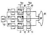
제 1 도에 도시한 바와 같이, 본 실시예의 증폭기는 전압-전류 변환방식의 전류증폭기(1)과 이 전류증폭기의 출력전류를 전압으로 변환해서 전압출력 VOUT를 얻기 위한 임피던스 소자 R200을 갖는다. 또, 출력단자 B의 직류전압레벨(바이어스)을 소정의 전위 Vref로 유지하기 위해서 오퍼레이션 증폭기(2)를 이용한 부귀환 회로가 마련되어 있다.As shown in FIG. 1, the amplifier of this embodiment has a
제 1 도의 저항 R210은 큰 저항값(예를들면 20kΩ)을 가지므로, B점에서, 본 임피던스는 크고 B점의 전위는 대략 라인 13의 전위(즉 Vref)와 동일하다.Since resistor R210 in FIG. 1 has a large resistance value (for example, 20 kΩ), at point B, the present impedance is large and the potential at point B is approximately equal to the potential at line 13 (ie, Vref ).
이 부귀환 루프는 클럭ψ 의해서 제어되는 스위치 SW가 닫혔을 때에 구성되고, 스위치 SW가 열려 있을 때에는 유지 캐패시터 C2에 의해서 직류 바이어스가 유지된다. 또, 저항(R230)은 그 저항값이 20kΩ으로 크게 설정되어 있다.This negative feedback loop is configured when the switch SW controlled by the clock ψ is closed,and the DC bias is held by the holding capacitor C2 when the switch SW is open. The resistance (R230) has its resistance value is set larger as 20kΩ.
전류증폭기(1)은 집적회로화 되어 있고, 그 전원전압 VCC1은 제 1 도에 도시한 바와 같이 예를들면 5V로 설정되어 있고, 전압-전류 변환용 저항 R200에 접속되는 전원전압 VCC2는 예를들면 200V로 설정되어 있다.The
(b) 특징점(b) feature points
전류증폭기(1)은 다음에 기술하는 바와 같이, 초미세화 프로세스 기술을 이용해서 집적회로화 되며 또한 주파수 특성이 나쁜 PNP트랜지스터는 1개도 사용하지 않고 능동소자로서 NPN트랜지스터만을 사용하고 있다.As described below, the
따라서, 전류증폭기(1)은 고속동작이 가능하고 주파수 특성이 양호하며, 200MHz 이상의 대역을 갖는다.Therefore, the
한편, 그 낮은 전원전압 VCC1임에도 불구하고 큰 출력을 얻기 위해서, 먼저 입력신호를 전류 IIN으로 변환하고, 그 전류 IIN을 기준으로 해서 n배화한 전류 nIIN을 마련하고 또한 이 nIIN의 전류를 m개 합성하여 결과적으로 n·m·IIN의 큰 전류를 얻는 방식을 채용하고 있다. 즉, 전류를 서서히 증폭하고 이 증폭된 전류를 합하는 것에 의해서, 어떠한 높은 내압소자(크기가 큰 소자 등)를 사용하지 않고도 높은 출력전류를 얻을 수가 있다.On the other hand, in spite of the low supply voltage VCC1, and to obtain a large output, first converting the input signal into a current IIN and to the basis of the current IIN provided a n a doubling current nIIN and also of the nIIN A method of synthesizing m currents and consequently obtaining a large current of n · m · IIN is adopted. In other words, by gradually amplifying the current and summing the amplified currents, a high output current can be obtained without using any high withstand voltage element (large size element, etc.).
본 실시예에서는 n=32, m=8로 설정되어, 결과적으로 IIn의 256배의 큰 출력전류를 얻을 수가 있다. 또 후술하겠지만 이 출력전류는 입력신호 VIN에 정확하게 대응해서 얻어진다. 또 마지막으로, 이 큰 출력전류를 저항 R200을 이용해서 전압변환하는 것에 의해서 결과적으로 증폭된 높은 출력전압을 얻을 수 있고, 이 증폭기는 매우 높은 전압증폭율을 가지며 출력 다이나믹 영역이 넓다.In this embodiment, n = 32 and m = 8 are set, and as a result, an output current of 256 times larger than IIn can be obtained. In addition, as will be described later, this output current is obtained in correspondence with the input signal VIN . Finally, voltage conversion of this large output current using a resistor R200 results in a high amplified output voltage. The amplifier has a very high voltage amplification factor and a wide output dynamic range.
제 1 도에서 명확한 바와 같이, 전류증폭기(전류증폭수단)(1)의 전원전압 VCC1은 5V로 설정되고, 제 3 도에 도시된 전류-전압 변환수단(전류-전압 변환회로)(400)의 전원전압 VCC2는 200V로 설정된다. 즉, 전류증폭기(1)의 전원전압 VCC1과 전류-전압 변환수단(400)의 전원전압 VCC2이 관계는 VCC1<VCC2은로 된다.As apparent from FIG. 1, the power supply voltage VCC1 of the current amplifier (current amplifier) 1 is set to 5V, and the current-voltage converter (current-voltage converter) 400 shown in FIG. The power supply voltage VCC2 of is set to 200V. That is, the relationship between the power supply voltage VCC1 of the
전류증폭기(1)의 전원전압 VCC1이 5V로 설정되는 이유는 200MHz에서 동작하는 전류증폭기(1)에 있어서, 전류증폭기(1)을 구성하는 회로소자의 소자크기를 매우 작게 하고 또 각 회로소자에 기생하는 기생용량을 최소한으로 하기 위함이다. 즉, 전류증폭기(1)을 소자크기가 큰 고내압 소자를 이용하지 않고 소자크기가 작은 저내압 소자를 이용해서 형성하기 위함이다.The reason why the power supply voltage VCC1 of the
그 결과, 전류증폭기(1)을 구성하는 회로소자는 고속동작이 가능하고 또한 고주파 특성이 양호하게 된다. 이것에 의해서, 후술하는 바와 같이 전류증폭기(1)은 집적회로(IC)화에도 적합한 구성으로 된다.As a result, the circuit elements constituting the
한편, 전류-전압 변환수단(400)은 전원전압 VCC2가 200V로 설정되는 이유는 다음과 같다.On the other hand, the reason why the current-voltage conversion means 400 is set to 200V the power supply voltage VCC2 is as follows.
전류-전압 변환수단(400)은 전류증폭기(1)에서 출력되는 큰 전류를 전압으로 변환해서 출력하는 기능을 갖는다. 전류-전압 변환수단(400)에서 출력되는 출력전압은 다음에 설명하는 제 3 도에 도시된 바와 같이, 컬러 디스플레이 장치내의 음극관(캐소드 레이 튜브 : CRT)(500)의 캐소드 K1, K2, K3으로의 인가전압으로서 이용된다. 캐소드 K1, K2, K3으로의 인가전압은 3원색으로 되는 적색, 녹색 및 청색의 각 전자총의 제어전압으로 되게 된다. 따라서, 캐소드 K1, K2, K3으로의 인가전압의 변화범위가 클수록, 즉 인가전압의 다이나믹 영역이 클수록 대응하는 전자총에서 출력되는 전자빔이 양을 매우 넓은 범위로 조정할 수 있게 된다. 이것은 음극관(500)에 의해서 미묘한 색채의 차이나 미묘한 휘도의 차이를 재현할 수 있다는 것을 의미한다.The current-voltage converting means 400 has a function of converting a large current output from the
이상의 이유에 의해, 전류-전압 변환수단(400)의 전원전압 VCC2는 전류증폭기(1)의 전원전압 VCC1(5V)보다 큰, 예를들면 200V와 같은 고전압으로 된다.For the above reasons, the power supply voltage VCC2 of the current-voltage converting means 400 is higher than the power supply voltage VCC1 (5V) of the
(c) 전류증폭기의 구체적 구성(c) specific configuration of the current amplifier;
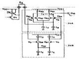
제 2 도는 전류증폭기(1)의 구체적인 회로구성을 도시한 것이다.2 shows a specific circuit configuration of the
제 2 도에 있어서 점선으로 둘러싸인 부분(1000)은 입력신호 VIN에 대응한 전류 IIN을 얻기 위한 전압-전류 변환회로이며, 마찬가지로 점선으로 둘러싸인 (1001)~(100m)은 전류 IIN을 n배하는 전류증폭기로서의 전류미러회로이다.In FIG. 2, the
이 m개(예를들면 m=8)의 전류미러회로의 출력단자를 C점에서 와이어드 접속하고, 여기에서 전류합성을 실행하는 것에 의해 출력선 l2에서 큰 출력전류 IOUT(IOUT=m·n·IIN)가 얻어진다.The large output current IOUT (IOUT = m) at the output line l2 by wire-connecting the output terminals of these m current mirror circuits at the point C, for example, and performing current synthesis here. N · IIN ) is obtained.
회로동작을 보다 구체적으로 설명하면 다음과 같다.The circuit operation will be described in more detail as follows.
즉, 입력신호 VIN은 라인 l1을 따라 커플링 커패시터 C1을 거쳐서 트랜지스터 Q200의 베이스로 입력되고, 그 에미터에서 입력전압에 대응하는 전류 IS를 얻는다. 이 전류 IS를 기준으로 해서 전류미러를 사용하여 여러개의 전류 IX를 마련하고, 전류 IX에서 이 전류 IS를 감산하는 것에 의해 입력신호 VIN에 대응해서 변화하는 전류 IN(IN=IX-IS)가 얻어져서 전류미러회로의 각각으로 입력된다.That is, the input signal VIN is input to the base of the transistor Q200 along the coupling capacitor C1 along the line l1 , and obtains a current IS corresponding to the input voltage at the emitter. Referenced to the current IS, using a current mirror providing a multiple of the current IX and the current changing in response to the input signal VIN by subtracting the current IS from the current IX IN (IN = IX -IS ) is obtained and input into each of the current mirror circuits.
이 전류 IIN을 또 전류미러회로 (1001)~(100m)을 이용해서 n배(32배)하고 또한 각자의 전류미러회로(1001)~(100m)의 출력을 합성해서, 결과적으로 IOUT(IOUT=m·n·IIN)을 얻는다.By again using a current mirror circuit (1001) ~ (100m) of the current IIN n times (32 times), and also by combining the outputs of each of the current mirror circuit (1001) ~ (100m), as a result IOUT ( IOUT = m · n · IIN ).
또, 입력 VIN에 정확하게 대응한 출력을 얻고 또한 주파수 특성을 양호하게 하기 위해서, 다음의 연구가 이루어지고 있다.In order to obtain an output corresponding to the input VIN accurately and to improve frequency characteristics, the following studies have been made.
즉, 제 2 도에서 명확한 바와 같이 여러개의 전류미러회로(1001)~(110m)이 마련하고, 또 각각의 전류미러회로에는 1개의 기준 트랜지스터에 대해서 출력 트랜지스터가 여러개(본 예에서는 3개) 마련되어 있다.That is, as shown in FIG. 2, a plurality of
큰 전류만을 얻기 위한 목적이라면 1개의 전류미러회로를 준비하고, 그 전류미러회로에서 1개의 기준 트랜지스터에 대해서 출력 트랜지스터를 여러개 마련하여 그 각각의 출력 트랜지스터의 출력을 합성하도록 해도 좋다.For the purpose of obtaining only a large current, one current mirror circuit may be prepared, and in the current mirror circuit, multiple output transistors may be provided for one reference transistor to synthesize the outputs of the respective output transistors.
그러나, 이 구성에서는 전류미러회로의 출력 트랜지스터에 있어서의 베이스와 컬랙터 사이에 기생하는 기생용량이 커져서 고주파 특성이 현저하게 악화되어 버린다.However, in this configuration, the parasitic capacitance between the base and the collector in the output transistor of the current mirror circuit increases, and the high frequency characteristic is significantly deteriorated.
이것은 IC화된 디바이스 구조를 생각하면 명확하게 된다.This is evident in light of the IC device structure.
제 7 도는 제 2 도에 도시한 전류미러회로(100)((1002)~(100m)도 동일하다)의 IC 디바이스의 단면도이다. 먼저, 전류미러회로(1001)의 구조에 대해서 간단하게 설명한다.FIG. 7 is a cross-sectional view of the IC device of the current mirror circuit 100 (also (1002) to (100m) is the same) shown in FIG. First, the structure of the
P-형 기판(3)상에 N-형 에피택셜층(5)가 마련되고, 그 기판(3)과 에피택셜층(5) 사이에는 N+형 매립층(4)가 부분적으로 형성되어 있다.An N-
N-형 에피택셜층에는 부분적으로 홈부(17)이 형성되고, 이 홈의 바닥부분과 P-형 기판(3)을 접속하는 P+분비층(6)에 의해서 N-형 에피택셜층은 여러개의 섬영역으로 분할되어 있다. 이 섬영역에도 포토 리도그래피 기술을 이용해서 NPN 트랜지스터 Q260, Q270이 각각 형성되어 있다. N-형 에피택셜층의 두께는 예를들면 1.7㎛, 트랜지스터의 베이스(7), (8)의 깊이는 예를들면 0.7㎛, 에미터(9), (10)의 깊이는 예를들면 0.4㎛로 되어 있어 매우 미세한 IC이다. 또, 에피택셜층(5)내에 부분적으로 마련된 홈부(17)에 의해서 분리층(6)의 가로방향으로의 확산을 최소한으로 억제할 수 있고, 또 트랜지스터의 컬렉터 직렬저항을 매우 작게 할 수가 있다. 이상의 설명에서 명확히 알 수 있는 바와 같이, 전류증폭기는 초미세화 프로세스 기술을 이용해서 형성되어 있어 고속동작이 가능하며 또한 고주파 특성이 매우 양호하다.N- type epitaxial layer has in part a groove 17 is formed and, a bottom portion of the groove and the P- by the P+ secretion layer 6 which connects the shaped substrate (3) N- type epitaxial layer has several It is divided into island regions of. In this island region, NPN transistors Q260 and Q270 are formed using photolithography techniques, respectively. The thickness of the N− type epitaxial layer is, for example, 1.7 μm, the depth of the
여기에서, 상술한 전류미러회로의 출력 트랜지스터의 베이스와 컬렉터 사이에 기생하는 부유용량 Cf에 대해서 생각한다. 제 7 도에서 알 수 있는 바와 같이, 전류미러회로의 각각의 출력 트랜지스터의 수가 증가하면 증가할수록 베이스와 컬렉터 사이의 부유용량 Cf및 컬렉터와 기판 사이의 기생용량 Cp가 증대하여 버린다. 따라서, 본 발명에서는 전류미러회로의 각각에 있어서의 출력 트랜지스터의 수를 어떤 일정값 이하로 억제하여 기생용량의 증대를 방지한다.Here, the parasitic stray capacitance Cf between the base and the collector of the output transistor of the current mirror circuit described above is considered. As can be seen in FIG. 7, as the number of output transistors of the current mirror circuit increases, the stray capacitance Cf between the base and the collector and the parasitic capacitance Cp between the collector and the substrate increase. Therefore, in the present invention, the number of output transistors in each of the current mirror circuits is suppressed to a certain value or less to prevent an increase in parasitic capacitance.
또, 전류미러회로에 있어서 1개의 기준 트랜지스터에 대해서 출력 트랜지스터 수가 많이 있으면, 각 트랜지스터의 베이스 전류에 기인하는 전류미러의 비의 정밀도의 악화가 발생한다. 이를 방지하고 입력신호 VIN에 대응한 정확한 출력전류를 얻기 위해서도, 출력 트랜지스터 수를 일정값을 이하로 억제하는 것은 유효하다.Moreover, when there are many output transistors with respect to one reference transistor in a current mirror circuit, the precision of the ratio of the current mirror resulting from the base current of each transistor will arise. In order to prevent this and to obtain an accurate output current corresponding to the input signal VIN , it is effective to keep the number of output transistors below a certain value.
(d) 전류미러회로에 있어서의 바이어스 전류의 온도 의존성의 저감을 위한 연구(d) Study for reducing temperature dependence of bias current in current mirror circuit
제 2 도에 도시한 전류미러회로에는 입력전류 IIN의 온도 의존심을 저감하기 위해서 중요한 연구가 이루어지고 있다. 즉, 전류미러회로의 입력 IIN은 IIN=IX-IS나타내고, 2개의 전류 IX와 IS의 차로서 얻어진다. 실제로, 이 전류 IX와 전류 IS는 IC의 주위온도가 변화했을 때에 동일하게 변화하도록 되어 있으며 (즉, 온도특성이 일치되어 있다), 결과적으로 주위의 온도가 변화하더라도 입력 IIN(IX-IS)은 대략 일정하게 정해진다.In the current mirror circuit shown in FIG. 2, important studies have been made to reduce the temperature dependency of the input current IIN . That is, the input IIN of the current mirror circuit represents IIN = IX -IS , and is obtained as a difference between two currents IX and IS. In practice, this current IX and current IS are supposed to change equally when the ambient temperature of the IC changes (i.e. the temperature characteristics are consistent), and as a result, the input IIN (IX -IS ) is approximately constant.
이것은 다음의 식으로 이해할 수 있다. 즉,This can be understood by the following equation. In other words,

식 (1)과 식 (2)에서 다음식이 얻어진다.The following equations are obtained from equations (1) and (2).

식 (3)의 제 3 항과 제 4 항에서 R61=R60+R110으로 선택하면, VBE가 들어간 항이 소멸되어 전류 IIN의 온도 의존성이 완전히 업어진다. 즉, 트랜지스터의 베이스와 에미터 사이의 전압 VBE는 약 -2mV/℃의 온도특성을 갖지만, 이 온도특성이 완전히 상쇄되어 전류미러회로의 입력전류 IIN은 주위의 온도에 관계없이 안전하다.If R61 = R60 + R110 is selected in the third and fourth terms of equation (3), the term containing VBE disappears and the temperature dependence of the current IIN is completely raised. That is, the voltage VBE between the base and the emitter of the transistor has a temperature characteristic of about -2 mV / ° C., but this temperature characteristic is completely canceled out so that the input current IIN of the current mirror circuit is safe regardless of the ambient temperature.
[실시예 2]Example 2
제 3 도는 본 발명의 제 2 실시예인 고정밀 디스플레이 장치의 구성을 도시한 것이다. 비디오 증폭기(300), (300'), (300")는 제 1 도에 전압-전류 변환방식의 전류증폭기에 해당하고, I/V(전류-전압 ) 변환수단(400), (400'), (400")는 제 1 도의 저향 R200에 해당한다. 비디오 증폭기(300), (300'), (300"), I/V 변환수단(400), (400'), (400")에 구체적 구성은 제 4 도와 제 5 도를 사용해서 다음에 상세하게 설명한다.3 shows the configuration of a high precision display device as a second embodiment of the present invention. The
(a) 전체구성(a) Overall composition
고정밀 디스플레이 장치는 제 3 도에 도시된 바와 같이, 중앙처리장치(CPU)(100), CPU(100)으로부터 송출되는 적(R), 녹(G), 청(B)의 각각의 디지탈 색신호를 아날로그 신호로 변환하는 D/A변환기(200), (200'), (200"), I/V변환수단(400), (400'), (400")와 CRT(500)으로 이루어진다.As shown in FIG. 3, the high-precision display device displays digital color signals of red (R), green (G), and blue (B) transmitted from the
CRT에 표시되는 영상의 휘도는 캐소드 K1, K2, K3의 인가전압에 의해서 제어되고, 색체는 R, G, B의 혼합비에 의해서 결정된다.The luminance of the image displayed on the CRT is controlled by the applied voltages of the cathodes K1 , K2 , K3 , and the color is determined by the mixing ratio of R, G, and B.
D/A변환기의 출력선 l3, l4, l5에는 예를들면 대역 200MHz의 고주파신호가 얻어져서 비디오증폭기(300), (300'), (300")로 입력된다. 비디오증폭기(300), (300'), (300")의 각각은 개별적으로 초미세화 프로세스 기술을 이용해서 전압-전류방식의 전류증폭기 내에 집적회로화되어 있다. 이들 비디오 증폭기에서 얻어지는 출력전류를 I/V로 변환하는 것에 의해 출력전압이 얻어지고, 이 출력전압은 캐소드 K1, K2, K3에 인가된다.The output lines l3 , l4 , l5 of the D / A converter obtain a high frequency signal of, for example, a band of 200 MHz and are input to the
이것에 의해, 캐소드로부터 전자가 방출되어 각 색의 형광소자(도시하지 않음)를 발광시켜 원하는 컬러영상을 얻는다.As a result, electrons are emitted from the cathode to emit light of fluorescent elements (not shown) of each color to obtain a desired color image.
이 CRT에 있어서의 주사선(래스터)는 1000줄 이상이므로, 매우 치밀한 영상이 얻어진다.Since the scanning line (raster) in this CRT is 1000 lines or more, a very dense image is obtained.
(b) 특징점(b) feature points
i ) 각각의 비디오 증폭기는 초미세화 프로세스 기술을 이용해서 IC화되어 있으므로, 고주파 특성이 양호하다.이것에 의해 전자빔을 초고속으로 주사할 수가 있다.i) Since each video amplifier is ICized using an ultra-fine process technology, the high frequency characteristic is good. This makes it possible to scan the electron beam at a very high speed.
ii ) 비디오 증폭기에서 큰 전류의 출력이 얻어지고, 이것을 마지막으로 전압변환하는 것에 의해 큰 출력전압이 얻어져서 출력 다이나믹 영역이 매우 넓다. 이 결과, 캐소드에 인가된 전압을 치밀하게 제어할 수 있어 미묘한 색채의 차이를 표현할 수가 있다.ii) A large current output is obtained in the video amplifier, and a large output voltage is obtained by finally converting the voltage so that the output dynamic range is very wide. As a result, it is possible to precisely control the voltage applied to the cathode and to express subtle color differences.
iii ) 각각의 비디오 증폭기는 개별적으로 IC화되어 있으므로, R, G, B의 각 신호 사이의 누화가 완전히 방지된다.iii) Since each video amplifier is individually ICized, crosstalk between R, G and B signals is completely prevented.
(c) 비디오 증폭기와 I/V변환수단의 구체적 전체구성(c) specific overall configuration of video amplifiers and I / V conversion means;
제 4 도는 비디오 증폭기와 I/V변환수단의 블럭도이다. 그리고, 제 5 도는 더욱 구체적 회로구성을 도시한 회로도이다.4 is a block diagram of a video amplifier and I / V conversion means. 5 is a circuit diagram showing a more specific circuit configuration.
먼저, 제 4 도에 따라서 설명한다. 제 4 도에 있어서 IC는 2개의 입력단자(①핀, ②핀)를 갖는 2개의 입력 VIN1, VIN2에 의한 합성영상신호를 얻을 수 있도록 되어 있다. (21A)와 (21B)는 TTL레벨의 신호 VIN1과 신호 VIN2를 받는 버퍼회로이다. 스위치S1, S2는 제어회로(23a)와 (23b)에 의해서 제어된다. 버퍼회로(21A)와 (21B)의 출력은 프리앰프(24)(이 프리앰프의 이득은 제어신호 Vc에 의해서 가변가능하다)를 거쳐서 전압-전류 변환방식의 전류증폭회로(25)로 입력된다. 전류증폭회로(25)의 출력은 IC의 외부에 마련된 I/V변환수단(400)의 I/V변환용 저항 RL에 의해 전압으로 변환된다. 트랜지스터 Q20과 Q22은 발진방지를 위해서 마련되어 있다. 또, 출력선 lOUT의 직류 바이어스를 안정하게 설정하기 위해서, 저항 R7과 R8, 오퍼레이션 증폭기(27a), 버퍼 증폭기(27b) 및 저항 RA(RB)로 구성되는 부귀환경로가 마련되어 있다.First, it demonstrates according to FIG. In Fig. 4, the IC is able to obtain a composite video signal by two inputs VIN1 and VIN2 having two input terminals (① pin and ② pin). (21A) and (21B) is a buffer circuit which receives a signal VIN1 and VIN2 signal of the TTL level. The switches S1 and S2 are controlled by the
부귀환경로에 마려된 스위치 S3은 제어회로(27c)에 의해 제어되고, 이 제어회로(27c)는 패디스틀 레벨 클램프 펄스(pedestal level clamp pulse) VD에 의해서 제어된다.The switch S3 finished in the negative environment path is controlled by the
이 페디스틀 레벨 클램프 펄스가 인가되는 타이밍을 제 8 도를 이용해서 설명한다.The timing at which this pedestal level clamp pulse is applied will be described with reference to FIG.
제 8 도는 출력선 lOTT로 나타내는 출력 색신호 VO를 도시한 것으로서, "H"는 수평동기신호이다. 상술한 페디스틀 레벨 클램프 펄스 VD는 도면중의 T기간동안에 인가되고, 이때에 부귀환을 거는 것에 의해서 페디스틀 레벨 P의 전위를 기준전위 Vref2에 고정시킨다.8 shows the output color signal VO represented by the output line lOTT , where "H" is a horizontal synchronization signal. The above-described pedestal level clamp pulse VD is applied during the period T in the figure, and the potential of the pedestal level P is fixed to the reference potential Vref2 by performing negative feedback at this time.
(d) 비디오 증폭기와 I/V변환수단의 구체적 회로구성(d) specific circuit arrangement of video amplifiers and I / V conversion means;
제 5 도는 제 4 도에 도시한 IC의 보다 구체적인 회로구성을 도시한 것이다. 제 5 도에서는 제 4 도와 동일한 부분에 동일부호를 붙이고 있다.FIG. 5 shows a more specific circuit configuration of the IC shown in FIG. In Fig. 5, the same reference numerals are given to the same parts as in Fig. 4.
버퍼회로(21A), (21B)는 입력신호를 받는 NPN트랜지스터 Q1(Q41)과 전류미러회로로 구성되어 있다. 스위치 S1(S2)는 트랜지스터를 이용한 다이오드 Q4(Q5)로 이루어진다. 스위치 S1과 제어신호 Va의 관계는 다음과 같다.The
가령, 제어신호 Va가 "H"레벨이면, 정전류원 IS9로부터 송출되는 정전류 I는 다이오드 Q35와 Q37을 거쳐서 트랜지스터 Q38의 베이스를 구동하여 트랜지스터 Q38이 "on"한다. 이것에 의해, 이 트랜지스터 Q38의 컬렉터는 대략 접지전위로 되어 다이오드 Q4가 역바이어스되어 신호전달이 저지된다.For example, when the control signal Va is at the "H" level, the constant current I sent from the constant current source IS9 drives the base of the transistor Q38 via the diodes Q35 and Q37 to turn on the transistor Q38 . As a result, the collector of this transistor Q38 becomes approximately ground potential, diode Q4 is reverse biased, and signal transmission is prevented.
한편, 제어신호 Va가 "L"레벨로 되면, 정전류원 IS9로부터 송출되는 전류는 다이오드 Q34를 거쳐서 Va입력단자 방향으로 분류되어 트랜지스터 Q38이 "off"한다. 이것에 의해, 다이오드 Q4의 애노드 전위가 상승하여 다이오드 Q4가 순바이어스되고, 이 다이오드는 레벨시프트 수단으로서 동작하여 신호전달이 실행된다.On the other hand, when the control signal Va is at the "L" level, the current sent from the constant current source IS9 is classified in the direction of the input terminal Va via the diode Q34 , and the transistor Q38 is "off". As a result, the anode potential of the diode Q4 is biased by the rising order of the diode Q4, a diode, a signal transmission is performed by the operation as the level shift means.
프리앰프(24A)는 베이스접지 트랜지스터 Q9, 트랜지스터 Q8및 저항 R5로 구성되는 정전류원과 부하저항 R4로 이루어진다. ⑦번째 핀에서 인가되는 제어전압 Vc에 의해서 트랜지스터 Q8의 베이스전위가 제어되어 결과적으로 바이어스전류가 변화되고, 이것에 의해 프리앰프의 이득이 정밀하게 제어된다.The
또, 프리앰프(24A)와 이 프리앰프(24A)의 이득을 정밀하게 조정하는 회로(24B)의 다른 회로구성이 제 9 도에 도시된다.Further, another circuit configuration of the
이득정밀 조정회로(24B)에 있어서의 차동쌍을 이루는 트랜지스터 Q56, Q57에 인가되는 제어전압 VQ와 VR을 변화시키는 것에 의해서, 결과적으로 프리앰프(24A)에 있어서의 전류 IX와 IY의 합성 전류량이 변화한다. 이것에 의해, 이득조정이 실행되도록 저항 R51에서 발생하는 전압강하가 변화한다. 또한, 정전류 IA와 IB는 그 전류량이 다르다.By varying the control voltages VQ and VR applied to the transistors Q56 and Q57 , which form the differential pairs in the gain
이 프리앰프의 출력을 받는 에미터플로워 Q10이후의 IC의 출력핀인 ⑨번째 핀까지의 회로구성이 제 2 도에 도시한 것과 동일하므로, 그 회로구성과 회로동작의 설명은 생략한다.Since the circuit configuration from the emitter follower Q10 to the ninth pin, which is the output pin of the IC after receiving the output of the preamplifier, is the same as that shown in Fig. 2, the description of the circuit configuration and circuit operation is omitted.
전압-전류(V/I) 변환수단(400)은 부하저항 R21과 발진방지용으로 마련된 트랜지스터 Q20및 Q21로 구성된다.The voltage-current (V / I) converting means 400 is composed of a load resistor R21 and transistors Q20 and Q21 provided for preventing oscillation.
부귀환 입력은 ⑩번째 핀에서 차동쌍을 이루는 트랜지스터 Q22와 Q23중 Q23의 베이스로 인가된다. 스위치 S3은 트랜지스터 Q28, Q29로 이루어진다. 패디스틀 레벨 클램프 펄스 VD("H"레벨)가 입력되며, 이제까지 ⑫핀방향으로 흐르고 있던 정전류원 ISS로부터 송출되는 전류는 이번에는 다이오드 Q34와 Q37坼 트랜지스터 Q32의 베이스를 구동하여 이것이 "on"한다. 이것에 의해, 스위치 S3을 구성하는 트랜지스터 Q28, Q29로 베이스전위가 공급되어 신호전달이 실행된다.The negative feedback input is applied to the base of Q23 of transistors Q22 and Q23 that are differentially paired at the pin. The switch S3 consists of transistors Q28 and Q29 . Paddy-level clamp pulse VD (“H” level) is input, and the current sent from the constant current source ISS that has flowed in the ⑫ pin direction now drives the base of diode Q34 and Q37坼 transistor Q32 . This is "on". As a result, the base potential is supplied to the transistors Q28 and Q29 constituting the switch S3 to perform signal transmission.
부귀환 신호는 버퍼 증폭기(27b)와 부귀환선 l10을 거쳐서 입력신호선 l3a,l3b로 귀환된다.The negative feedback signal is fed back to the input signal lines l3a and l3b via the
[실시예 3]Example 3
제 6 도는 본 발명의 다른 실시예를 도시한 것이다. 이 고정밀 디스플레이 장치의 회로구성은 대략 제2실시예와 동일하지만, 상이한 점은 R, G, B의 각 색신호용 비디오 증폭기가 일체적으로 IC화되어 있는 점과 I/V변환수단도 IC화되어 있다는 점이다.6 shows another embodiment of the present invention. The circuit configuration of this high-precision display device is substantially the same as in the second embodiment, except that the video amplifiers for the color signals of R, G, and B are integrally integrated with the IC, and the I / V conversion means are integrated with the IC. Is that there is.
각각의 비디오 증폭기가 일체적으로 IC화되는 것에 의해서, 각 증폭기의 온도특성(주위의 온도를 변경하였을때의 증폭율의 변화)이 일치한다.By integrated IC of each video amplifier, the temperature characteristics of each amplifier (change in amplification rate when the ambient temperature is changed) coincide.
또, I/V변환수단도 IC화되는 것에 의해서, 디스플레이 장치를 보다 컴팩트하게 구성할 수가 있다.In addition, since the I / V conversion means is also IC, the display device can be configured more compactly.
IC(401)은 고내압 소자 프로세스 기술을 이용해서 제조된다.
이상, 본 발명자에 의해서 이루어진 발명을 상기 실시예에 따라서 구체적으로 설명하였지만, 본 발명은 상기 실시예에 한정되는 것은 아니고 그 요지을 이탈하지 않는 범위내에서 여러가지로 변경가능한 것은 물론이다.As mentioned above, although the invention made by this inventor was demonstrated concretely according to the said Example, this invention is not limited to the said Example and can be variously changed in the range which does not deviate from the summary.
Claims (25)
Translated fromKoreanPriority Applications (1)
| Application Number | Priority Date | Filing Date | Title |
|---|---|---|---|
| KR1019910002449AKR950003137B1 (en) | 1985-04-03 | 1991-02-13 | Amplifier and display device |
Applications Claiming Priority (6)
| Application Number | Priority Date | Filing Date | Title |
|---|---|---|---|
| JP60068928AJPH06105961B2 (en) | 1985-04-03 | 1985-04-03 | Amplifier circuit |
| JP60068929AJPH0628384B2 (en) | 1985-04-03 | 1985-04-03 | Amplifier circuit |
| JP60068930AJPH06105962B2 (en) | 1985-04-03 | 1985-04-03 | Amplifier circuit |
| JP60-68928 | 1985-04-03 | ||
| JP60-68929 | 1985-04-03 | ||
| JP60-68930 | 1985-04-03 |
Related Child Applications (1)
| Application Number | Title | Priority Date | Filing Date |
|---|---|---|---|
| KR1019910002449ADivisionKR950003137B1 (en) | 1985-04-03 | 1991-02-13 | Amplifier and display device |
Publications (2)
| Publication Number | Publication Date |
|---|---|
| KR860008690A KR860008690A (en) | 1986-11-17 |
| KR950003135B1true KR950003135B1 (en) | 1995-04-01 |
Family
ID=27299904
Family Applications (1)
| Application Number | Title | Priority Date | Filing Date |
|---|---|---|---|
| KR1019860001129AExpired - Fee RelatedKR950003135B1 (en) | 1985-04-03 | 1986-02-19 | Amplifier and display device |
Country Status (2)
| Country | Link |
|---|---|
| US (2) | US4755768A (en) |
| KR (1) | KR950003135B1 (en) |
Families Citing this family (12)
| Publication number | Priority date | Publication date | Assignee | Title |
|---|---|---|---|---|
| KR950003135B1 (en)* | 1985-04-03 | 1995-04-01 | 가부시기가이샤 히다찌세이사꾸쇼 | Amplifier and display device |
| US5724519A (en)* | 1989-02-17 | 1998-03-03 | Hitachi, Ltd. | Complementary transistor circuit and amplifier and CRT display device using the same |
| US5734366A (en)* | 1993-12-09 | 1998-03-31 | Sharp Kabushiki Kaisha | Signal amplifier, signal amplifier circuit, signal line drive circuit and image display device |
| JP3135810B2 (en)* | 1995-01-31 | 2001-02-19 | シャープ株式会社 | Image display device |
| JP3549441B2 (en)* | 1998-06-22 | 2004-08-04 | シャープ株式会社 | Constant current controller |
| US6972016B2 (en)* | 2001-05-01 | 2005-12-06 | Cardima, Inc. | Helically shaped electrophysiology catheter |
| RU2223507C2 (en)* | 2001-10-12 | 2004-02-10 | Открытое акционерное общество Раменское приборостроительное конструкторское бюро | Circuit to process signal from strain-gauge transducer to serial code |
| RU2265229C2 (en)* | 2003-10-14 | 2005-11-27 | Открытое акционерное общество Раменское приборостроительное конструкторское бюро | Circuit for processing signal from strain-resistive sensor |
| TWI275243B (en)* | 2005-09-14 | 2007-03-01 | Princeton Technology Corp | Voltage controlled amplifier for a signal processing system |
| RU2388000C2 (en)* | 2008-06-16 | 2010-04-27 | Ирина Андреевна Евтюхина | Method for measuring bridge signal processing and device for its implementation |
| US10056898B2 (en)* | 2015-09-30 | 2018-08-21 | Mediatek Inc. | Input stage of chip and method for controlling source driver of chip |
| US10145734B2 (en)* | 2016-08-22 | 2018-12-04 | Semiconductor Components Industries, Llc | Methods and apparatus for a light sensor |
Family Cites Families (2)
| Publication number | Priority date | Publication date | Assignee | Title |
|---|---|---|---|---|
| US4502020A (en)* | 1983-10-26 | 1985-02-26 | Comlinear Corporation | Settling time reduction in wide-band direct-coupled transistor amplifiers |
| KR950003135B1 (en)* | 1985-04-03 | 1995-04-01 | 가부시기가이샤 히다찌세이사꾸쇼 | Amplifier and display device |
- 1986
- 1986-02-19KRKR1019860001129Apatent/KR950003135B1/ennot_activeExpired - Fee Related
- 1986-04-03USUS06/847,721patent/US4755768A/ennot_activeExpired - Lifetime
- 1988
- 1988-05-04USUS07/190,050patent/US4888561A/ennot_activeExpired - Lifetime
Also Published As
| Publication number | Publication date |
|---|---|
| US4755768A (en) | 1988-07-05 |
| KR860008690A (en) | 1986-11-17 |
| US4888561A (en) | 1989-12-19 |
Similar Documents
| Publication | Publication Date | Title |
|---|---|---|
| KR950003135B1 (en) | Amplifier and display device | |
| EP0108428A1 (en) | Differential amplifier circuit with rail-to-rail capability | |
| US5757233A (en) | Complementary transistor circuit and amplifier and CRT display device using the same | |
| KR0148324B1 (en) | Variable gain amplifier circuit | |
| JPH0229169A (en) | Wide band ab class crt cathode drive circuit | |
| JPS6359310B2 (en) | ||
| US3956645A (en) | Controllable current source | |
| US4442458A (en) | CRT Video drive circuit with beam current stabilization | |
| KR950003137B1 (en) | Amplifier and display device | |
| US6295098B1 (en) | Illumination intensity correcting circuit | |
| JPH0554689A (en) | Sample and hold circuit and buffer circuit and sample and hold device using above circuits | |
| Gratz | Operational transconductance amplifiers | |
| NL8502343A (en) | DIGITAL VIDEO SIGNAL PROCESSING SYSTEM. | |
| FI66103B (en) | VIDEOSIGNALEN KOMBINERANDE ANORDNING | |
| JP2896029B2 (en) | Voltage-current converter | |
| US5339044A (en) | High linearity differential circuit | |
| Wilson et al. | Improved logarithmic converter based on a transconductance feedback amplifier | |
| US3955147A (en) | Amplifier circuit | |
| US6573669B1 (en) | Cathode ray tube driver circuit with frequency compensation without providing a leakage path for cathode current | |
| US5973314A (en) | Photoelectric converting device which prevents power source ripple from mixing into an output signal | |
| JPH0474010A (en) | Differential amplifier | |
| US6538398B1 (en) | Cathode ray tube driver circuit with cathode current detection | |
| SU930580A1 (en) | Differential current amplifier | |
| US4499429A (en) | Variable gain control circuit | |
| KR830000542B1 (en) | Gain control circuit |
Legal Events
| Date | Code | Title | Description |
|---|---|---|---|
| PA0109 | Patent application | St.27 status event code:A-0-1-A10-A12-nap-PA0109 | |
| R17-X000 | Change to representative recorded | St.27 status event code:A-3-3-R10-R17-oth-X000 | |
| PG1501 | Laying open of application | St.27 status event code:A-1-1-Q10-Q12-nap-PG1501 | |
| A201 | Request for examination | ||
| P11-X000 | Amendment of application requested | St.27 status event code:A-2-2-P10-P11-nap-X000 | |
| P13-X000 | Application amended | St.27 status event code:A-2-2-P10-P13-nap-X000 | |
| PA0201 | Request for examination | St.27 status event code:A-1-2-D10-D11-exm-PA0201 | |
| E902 | Notification of reason for refusal | ||
| PE0902 | Notice of grounds for rejection | St.27 status event code:A-1-2-D10-D21-exm-PE0902 | |
| T11-X000 | Administrative time limit extension requested | St.27 status event code:U-3-3-T10-T11-oth-X000 | |
| T11-X000 | Administrative time limit extension requested | St.27 status event code:U-3-3-T10-T11-oth-X000 | |
| P11-X000 | Amendment of application requested | St.27 status event code:A-2-2-P10-P11-nap-X000 | |
| P13-X000 | Application amended | St.27 status event code:A-2-2-P10-P13-nap-X000 | |
| G160 | Decision to publish patent application | ||
| PG1605 | Publication of application before grant of patent | St.27 status event code:A-2-2-Q10-Q13-nap-PG1605 | |
| E701 | Decision to grant or registration of patent right | ||
| PE0701 | Decision of registration | St.27 status event code:A-1-2-D10-D22-exm-PE0701 | |
| GRNT | Written decision to grant | ||
| PR0701 | Registration of establishment | St.27 status event code:A-2-4-F10-F11-exm-PR0701 | |
| PR1002 | Payment of registration fee | St.27 status event code:A-2-2-U10-U11-oth-PR1002 Fee payment year number:1 | |
| PR1001 | Payment of annual fee | St.27 status event code:A-4-4-U10-U11-oth-PR1001 Fee payment year number:4 | |
| R18-X000 | Changes to party contact information recorded | St.27 status event code:A-5-5-R10-R18-oth-X000 | |
| PN2301 | Change of applicant | St.27 status event code:A-5-5-R10-R13-asn-PN2301 St.27 status event code:A-5-5-R10-R11-asn-PN2301 | |
| PR1001 | Payment of annual fee | St.27 status event code:A-4-4-U10-U11-oth-PR1001 Fee payment year number:5 | |
| PR1001 | Payment of annual fee | St.27 status event code:A-4-4-U10-U11-oth-PR1001 Fee payment year number:6 | |
| PR1001 | Payment of annual fee | St.27 status event code:A-4-4-U10-U11-oth-PR1001 Fee payment year number:7 | |
| FPAY | Annual fee payment | Payment date:20020325 Year of fee payment:8 | |
| PR1001 | Payment of annual fee | St.27 status event code:A-4-4-U10-U11-oth-PR1001 Fee payment year number:8 | |
| LAPS | Lapse due to unpaid annual fee | ||
| PC1903 | Unpaid annual fee | St.27 status event code:A-4-4-U10-U13-oth-PC1903 Not in force date:20030402 Payment event data comment text:Termination Category : DEFAULT_OF_REGISTRATION_FEE | |
| PC1903 | Unpaid annual fee | St.27 status event code:N-4-6-H10-H13-oth-PC1903 Ip right cessation event data comment text:Termination Category : DEFAULT_OF_REGISTRATION_FEE Not in force date:20030402 | |
| R18-X000 | Changes to party contact information recorded | St.27 status event code:A-5-5-R10-R18-oth-X000 | |
| P22-X000 | Classification modified | St.27 status event code:A-4-4-P10-P22-nap-X000 |