KR940001251B1 - Voltage control circuit - Google Patents
Voltage control circuitDownload PDFInfo
- Publication number
- KR940001251B1 KR940001251B1KR1019900001909AKR900001909AKR940001251B1KR 940001251 B1KR940001251 B1KR 940001251B1KR 1019900001909 AKR1019900001909 AKR 1019900001909AKR 900001909 AKR900001909 AKR 900001909AKR 940001251 B1KR940001251 B1KR 940001251B1
- Authority
- KR
- South Korea
- Prior art keywords
- voltage
- voltage control
- circuit
- control circuit
- channel mos
- Prior art date
- Legal status (The legal status is an assumption and is not a legal conclusion. Google has not performed a legal analysis and makes no representation as to the accuracy of the status listed.)
- Expired - Fee Related
Links
Images


Classifications
- G—PHYSICS
- G05—CONTROLLING; REGULATING
- G05F—SYSTEMS FOR REGULATING ELECTRIC OR MAGNETIC VARIABLES
- G05F3/00—Non-retroactive systems for regulating electric variables by using an uncontrolled element, or an uncontrolled combination of elements, such element or such combination having self-regulating properties
- G05F3/02—Regulating voltage or current
- G05F3/08—Regulating voltage or current wherein the variable is DC
- G05F3/10—Regulating voltage or current wherein the variable is DC using uncontrolled devices with non-linear characteristics
- G05F3/16—Regulating voltage or current wherein the variable is DC using uncontrolled devices with non-linear characteristics being semiconductor devices
- G05F3/20—Regulating voltage or current wherein the variable is DC using uncontrolled devices with non-linear characteristics being semiconductor devices using diode- transistor combinations
- G05F3/205—Substrate bias-voltage generators
- G—PHYSICS
- G11—INFORMATION STORAGE
- G11C—STATIC STORES
- G11C5/00—Details of stores covered by group G11C11/00
- G11C5/14—Power supply arrangements, e.g. power down, chip selection or deselection, layout of wirings or power grids, or multiple supply levels
- G11C5/147—Voltage reference generators, voltage or current regulators; Internally lowered supply levels; Compensation for voltage drops
- G—PHYSICS
- G05—CONTROLLING; REGULATING
- G05F—SYSTEMS FOR REGULATING ELECTRIC OR MAGNETIC VARIABLES
- G05F3/00—Non-retroactive systems for regulating electric variables by using an uncontrolled element, or an uncontrolled combination of elements, such element or such combination having self-regulating properties
- G05F3/02—Regulating voltage or current
- G05F3/08—Regulating voltage or current wherein the variable is DC
- G05F3/10—Regulating voltage or current wherein the variable is DC using uncontrolled devices with non-linear characteristics
- G05F3/16—Regulating voltage or current wherein the variable is DC using uncontrolled devices with non-linear characteristics being semiconductor devices
- G05F3/20—Regulating voltage or current wherein the variable is DC using uncontrolled devices with non-linear characteristics being semiconductor devices using diode- transistor combinations
- G05F3/24—Regulating voltage or current wherein the variable is DC using uncontrolled devices with non-linear characteristics being semiconductor devices using diode- transistor combinations wherein the transistors are of the field-effect type only
- G—PHYSICS
- G11—INFORMATION STORAGE
- G11C—STATIC STORES
- G11C16/00—Erasable programmable read-only memories
- G11C16/02—Erasable programmable read-only memories electrically programmable
- G11C16/06—Auxiliary circuits, e.g. for writing into memory
- G11C16/30—Power supply circuits
- G—PHYSICS
- G11—INFORMATION STORAGE
- G11C—STATIC STORES
- G11C5/00—Details of stores covered by group G11C11/00
- G11C5/14—Power supply arrangements, e.g. power down, chip selection or deselection, layout of wirings or power grids, or multiple supply levels
- G11C5/145—Applications of charge pumps; Boosted voltage circuits; Clamp circuits therefor
- H—ELECTRICITY
- H02—GENERATION; CONVERSION OR DISTRIBUTION OF ELECTRIC POWER
- H02M—APPARATUS FOR CONVERSION BETWEEN AC AND AC, BETWEEN AC AND DC, OR BETWEEN DC AND DC, AND FOR USE WITH MAINS OR SIMILAR POWER SUPPLY SYSTEMS; CONVERSION OF DC OR AC INPUT POWER INTO SURGE OUTPUT POWER; CONTROL OR REGULATION THEREOF
- H02M3/00—Conversion of DC power input into DC power output
- H02M3/02—Conversion of DC power input into DC power output without intermediate conversion into AC
- H02M3/04—Conversion of DC power input into DC power output without intermediate conversion into AC by static converters
- H02M3/06—Conversion of DC power input into DC power output without intermediate conversion into AC by static converters using resistors or capacitors, e.g. potential divider
- H02M3/07—Conversion of DC power input into DC power output without intermediate conversion into AC by static converters using resistors or capacitors, e.g. potential divider using capacitors charged and discharged alternately by semiconductor devices with control electrode, e.g. charge pumps
- H02M3/073—Charge pumps of the Schenkel-type
- H—ELECTRICITY
- H10—SEMICONDUCTOR DEVICES; ELECTRIC SOLID-STATE DEVICES NOT OTHERWISE PROVIDED FOR
- H10D—INORGANIC ELECTRIC SEMICONDUCTOR DEVICES
- H10D89/00—Aspects of integrated devices not covered by groups H10D84/00 - H10D88/00
- H10D89/60—Integrated devices comprising arrangements for electrical or thermal protection, e.g. protection circuits against electrostatic discharge [ESD]
- H10D89/601—Integrated devices comprising arrangements for electrical or thermal protection, e.g. protection circuits against electrostatic discharge [ESD] for devices having insulated gate electrodes, e.g. for IGFETs or IGBTs
- H10D89/811—Integrated devices comprising arrangements for electrical or thermal protection, e.g. protection circuits against electrostatic discharge [ESD] for devices having insulated gate electrodes, e.g. for IGFETs or IGBTs using FETs as protective elements
- H10D89/819—Bias arrangements for gate electrodes of FETs, e.g. RC networks or voltage partitioning circuits
Landscapes
- Engineering & Computer Science (AREA)
- Power Engineering (AREA)
- Physics & Mathematics (AREA)
- Microelectronics & Electronic Packaging (AREA)
- Nonlinear Science (AREA)
- Electromagnetism (AREA)
- General Physics & Mathematics (AREA)
- Radar, Positioning & Navigation (AREA)
- Automation & Control Theory (AREA)
- Semiconductor Integrated Circuits (AREA)
- Dc-Dc Converters (AREA)
- Dram (AREA)
Abstract
Translated fromKoreanDescription
Translated fromKorean제1도는 본 발명에 따른 전압제어회로가 내장된 반도체 집적회로의 일부를 나타낸 구성설명도.1 is a schematic diagram showing a part of a semiconductor integrated circuit having a voltage control circuit according to the present invention;
제2도는 제1도중의 전압제어회로의 1실시예를 나타낸 회로도.2 is a circuit diagram showing an embodiment of the voltage control circuit in FIG.
제3도는 제2도에 나타낸 전압제어회로의 제어특성을 나타낸 도면.3 is a diagram showing control characteristics of the voltage control circuit shown in FIG.
제4도는 제2도에 나타낸 전압제어회로의 전압-전류 특성을 나타낸 도면.4 is a diagram showing the voltage-current characteristics of the voltage control circuit shown in FIG.
제5도는 제2도에 나타낸 전압제어회로중 MOS 트랜지스터의 일부를 나타낸 단면도.FIG. 5 is a cross-sectional view showing a part of a MOS transistor in the voltage control circuit shown in FIG.
제6도는 종래의 전압제어회로가 내장된 반도체 집적회로의 일부를 나타낸 구성설명도.6 is a schematic diagram showing a part of a semiconductor integrated circuit in which a conventional voltage control circuit is incorporated.
제7도는 제6도중의 종래의 전압제어회로를 나타낸 회로도이다.7 is a circuit diagram showing a conventional voltage control circuit in FIG.
* 도면의 주요부분에 대한 부호의 설명* Explanation of symbols for main parts of the drawings
1 : 전압입력단 2 : 승압회로1: voltage input 2: boost circuit
3 : 전압제어회로 4 : 인버터3: voltage control circuit 4: inverter
a : 승압회로의 전압출력단 P1=Pn : P채널 MOS 트랜지스터a: voltage output terminal of the boost circuit P1 = Pn: P-channel MOS transistor
[산업상의 이용분야][Industrial use]
본 발명은 반도체 집적회로에 설치되는 전압제어회로에 관한 것으로, 특히 제어대상인 전압발생회로의 출력전압을 일정레벨로 제어하는 전압제어회로에 관한 것이다.BACKGROUND OF THE
[종래의 기술 및 그 문제점][Traditional Technology and Problems]
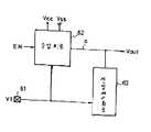
불휘발성 메모리가 내장된 반도체 집적회로에 있어서는, 예컨대 제6도에 나타낸 바와 같이 외부에 전압입력단(61)을 경유해서 공급되는 전압입력(V1)으로부터 예컨대 기입용의 고전압을 발생시키기 위한 승압회로(62)의 출력측에 출력전압(Vout)의 레벨을 일정하게 제어하기 위한 전압제어회로(63)가 설치되어 있다. 단, 제6도에서 참조부호 Vcc는 통상의 전원전압, Vss는 접지단위, EN은 활성화제어신호이다.In a semiconductor integrated circuit incorporating a nonvolatile memory, for example, as shown in FIG. 6, a booster circuit for generating, for example, a high voltage for writing from a voltage input V1 supplied via a
제7도는 종래의 전압제어회로를 도시해 놓은 구성도로서, 종래의 전압제어회로는 제어대상인 전압발생회로의 전압출력단과 기준전위단[즉, 승압회로(62)의 전압출력단(a)과 전압입력단(61)]의 사이에 각각 드레인·게이트가 서로 접속됨과 더불어 직렬접속된 복수개(n개)의 N채널 절연게이트형(MOS) 트랜지스터(N1-Nn)가 접속된 구성으로 되어, 승압회로(62)의 출력전압(Vout)를 N채널 MOS 트랜지스터(N1- Nn )의 접속단의 수에 따라 일정레벨로 제어하도록 되어 있다.FIG. 7 is a block diagram showing a conventional voltage control circuit. The conventional voltage control circuit includes a voltage output terminal and a reference potential terminal of the voltage generating circuit to be controlled (ie, the voltage output terminal a and the voltage of the booster circuit 62). The drain and gate are connected to each other between the
그러나, 이와 같은 구조로 된 종래의 전압제어회로(63)에 있어서는 백게이트 바이어스 효과에 의해 N채널 MOS 트랜지스터(N1-Nn)의 특성오차가 커지기 때문에 원하는 전압제어특성을 얻기 위한 N채널 MOS 트랜지스터의 접속단의 수를 설정하기가 어렵게 된다. 따라서, 전압제어특성의 신뢰성이 낮아지게 된다.However, in the conventional
여기서, 백게이트 바이어스라는 것은 MOSFET의 소오스·드레인영역간에 존재하는 채널영역에 대해 게이트전극으로부터 전위를 인가하는 것이 아니라 그 반대의 반도체기판측으로부터 직접 전위를 인가하는 것을 의미하는 것이다. 따라서, 채널영역에 전위가 인가되기 때문에 당연히 채널 도통에 필요한 게이트전극에 대한 인가전압치(임계치전압)가 영향을 받게 되는데, 이와 같은 것을 백게이트 바이어스 효과라고 부른다.Here, the back gate bias means not applying a potential from the gate electrode to a channel region existing between the source and drain regions of the MOSFET but directly applying the potential from the semiconductor substrate side opposite thereto. Therefore, since the potential is applied to the channel region, the applied voltage value (threshold voltage) to the gate electrode necessary for channel conduction is affected. This is called a back gate bias effect.
백게이트 바이어스 효과는 N채널형 MOSFET의 경우, 소오소영역의 전위에 대해 채널영역의 전위가 정(正)으로 되면, 임계치전압이 낮아지게 되고, 반대로 소오스영역의 전위에 대해 채널영역의 전위가 부(負)로 되면, 임계치전압이 높아지도록 나타난다. 여기서, N채널형 MOSFET는 통상적으로는 P형 반도체기판에 직접 소오스영역 및 드레인영역을 형성하기 때문에 당연히 채널영역의 전위는 반도체기판의 전위(Vss)인 볼트로 되자만, 전원전압 변동등의 영향을 받아 채널영역의 전위는 반드시 안정되지 않아 변동하여 버린다.The back gate bias effect is that when the potential of the channel region becomes positive with respect to the potential of the source region in the case of the N-channel MOSFET, the threshold voltage is lowered. If negative, the threshold voltage appears to be high. Here, since the N-channel MOSFET typically forms the source region and the drain region directly on the P-type semiconductor substrate, naturally the potential of the channel region becomes volt, which is the potential (Vss) of the semiconductor substrate. As a result, the potential of the channel region is not always stable, and thus fluctuates.
또, 전압제어회로(63)는 승압회로(62)로부터 고전압이 급격히 인가되면, 이 고전압은 그것이 직접 드레인에 인가되는 N채널 MOS 트랜지스터(N1)의 드레인·소오스간에 급격히 걸리게 되므로 그 N채널 MOS 트랜지스터(N1)의 신뢰성에 영향을 미치게 된다. 그리고 이 N채널 MOS 트랜지스터(N1)에 단락등이 생기게 되면 전압제어특성이 열화되어 최악의 경우에는 전압제어가 불가능하게 되는데, 이 때문에 전압제어회로(63)가 삽입된 직접회로의 신뢰성이 낮아지게 된다.When the high voltage is suddenly applied from the
즉, 이상 설명한 바와 같이 종래의 전압제어회로는 원하는 전압제어특성을 얻기 위한 N채널 MOS 트랜지스터의 접속단의 수를 설정하기가 어렵게 되므로 전압제어특성의 신뢰성이 낮다는 문제점이 있다.That is, as described above, the conventional voltage control circuit has a problem in that the reliability of the voltage control characteristic is low because it is difficult to set the number of connection terminals of the N-channel MOS transistor for obtaining the desired voltage control characteristic.
또, 종래의 전압제어회로는 제어대상인 전압발생회로로부터 고전압이 급격히 인가되면, 전압제어특성이 열화되어 최악의 경우에는 전압제어가 불가능하게 됨으로써 이 전압제어회로가 삽입된 집적회로의 신뢰성도 낮아지게 되는 문제점이 있다.In the conventional voltage control circuit, when a high voltage is suddenly applied from the voltage generation circuit to be controlled, the voltage control characteristic is degraded, and in the worst case, voltage control is impossible, thereby reducing the reliability of the integrated circuit into which the voltage control circuit is inserted. There is a problem.
[발명의 목적][Purpose of invention]
본 발명은 상기 문제점을 감안하여 발명된 것으로, 원하는 전압제어특성을 얻기 위한 MOS 트랜지스터의 접속단의 수를 용이하게 설정할 수 있게 됨으로써 전압제어특성의 신뢰성을 향상시킬 수 있도록 전압제어회로를 제공함에 그 목적이 있다.SUMMARY OF THE INVENTION The present invention has been invented in view of the above problems, and it is possible to easily set the number of connection terminals of a MOS transistor for obtaining a desired voltage control characteristic, thereby providing a voltage control circuit for improving the reliability of the voltage control characteristic. There is a purpose.
또, 본 발명은 제어대상인 전압발생회로로부터 고전압이 급격히 인가되어도 이 고전압에 의해 MOS 트랜지스터의 신뢰성이 저하되는 것을 방지할 수 있고, 더욱이 상기 전압발생회로로부터 전압이 입력되지 않을 때에는 직류전류에 의한 불필요한 소비전류가 방지되는 전압제어회로를 제공함에 그 목적이 있다.In addition, the present invention can prevent the reliability of the MOS transistor from being deteriorated by the high voltage even when a high voltage is suddenly applied from the voltage generation circuit to be controlled. Furthermore, when the voltage is not input from the voltage generation circuit, it is unnecessary by the DC current. It is an object of the present invention to provide a voltage control circuit in which current consumption is prevented.
또 본 발명은 테스트시 등에 제어대상인 전압발생회로의 기준전위측의 출력단의 전위가 이 전압제어회로의 전압출력단의 전위보다 높게 되어도 불필요한 직류전류가 흐르는 것이 방지되도록 된 전압제어회로를 제공함에 그 목적이 있다.Another object of the present invention is to provide a voltage control circuit in which unnecessary DC current is prevented from flowing even when the potential of the output terminal on the reference potential side of the voltage generation circuit to be controlled is higher than the potential of the voltage output terminal of the voltage control circuit during testing. There is this.
[발명의 구성][Configuration of Invention]
상기 목적을 달성하기 위한 본 발명의 제1실시예에 따른 전압제어회로는 반도체 집적회로에 설치된 제어 대상인 전압제어회로의 전압출력단과 기준전위단의 사이에 각각 소오스·기판이 서로 접속됨과 더불어 각각 게이트·드레인이 서로 접속된 복수개의 P채널 MOS 트랜지스터가 직렬로 접속된 구성으로 되어 있다.In the voltage control circuit according to the first embodiment of the present invention for achieving the above object, a source and a substrate are connected to each other between a voltage output terminal and a reference potential terminal of a voltage control circuit to be controlled in a semiconductor integrated circuit. A plurality of P-channel MOS transistors connected with drains are connected in series.
또, 상기 목적을 달성하기 위한 본 발명의 제2실시예에 따른 전압제어회로는 상기 제1실시예의 전압제어회로에 있어서, 전압발생회로의 전압출력단과 상기 직렬접속된 복수개의 P채널 MOS 트랜지스터의 일단측 사이에 소오스·기판이 서로 접속됨과 더불어 게이트에 상기 제어대상인 전압발생회로의 활성화제어신호에 동기되어 활성화제어신호가 공급되는 1개의 P채널 MOS 트랜지스터가 부가삽입된 구성으로 되어 있다 .In addition, the voltage control circuit according to the second embodiment of the present invention for achieving the above object is a voltage control circuit of the first embodiment, the voltage output terminal of the voltage generating circuit and the plurality of P-channel MOS transistors connected in series The source and substrate are connected to one end and an additional P-channel MOS transistor to which the activation control signal is supplied in synchronization with the activation control signal of the voltage generation circuit to be controlled is additionally inserted into the gate.
또, 본 발명의 제3실시예에 따른 전압제어회로는 상기 제1 또는 제2실시예의 전압제어회로에 있어서, 직력접속된 복수개의 P채널 MOS 트랜지스터의 다른단측과 상기 전압발생회로의 기준전위단 사이에 기판·게이트·드레인이 서로 접속되어 있는 1개의 P채널 MOS 트랜지스터 또는 1개의 다이오드가 부가삽입된 구성으로 되어 있다.Further, in the voltage control circuit according to the third embodiment of the present invention, in the voltage control circuit of the first or second embodiment, the other end side of the plurality of series-connected P-channel MOS transistors and the reference potential end of the voltage generation circuit are provided. One P-channel MOS transistor or one diode in which substrates, gates and drains are connected to each other is additionally inserted.
[작용][Action]
상기와 같이 구성된 본 발명의 제1실시예에 따른 전압제어회로는 복수개의 P채널 MOS 트랜지스터가 사용되고 있으므로 백게이트 바이어스 효과를 많이 받지 않게 된다. 따라서, 원하는 전압제어특성을 얻기 위한 P채널 MOS 트랜지스터의 접속단의 수를 용이하게 설정할 수 있게 됨으로써 전압제어특성의 신뢰성이 향상된다.In the voltage control circuit according to the first embodiment of the present invention configured as described above, since a plurality of P-channel MOS transistors are used, the back gate bias effect is not largely affected. Therefore, the number of connection terminals of the P-channel MOS transistors for obtaining the desired voltage control characteristics can be easily set, thereby improving the reliability of the voltage control characteristics.
또, 본 발명의 제2실시예에 따른 전압제어회로는 제어대상인 전압발생회로로부터 고전압이 급격히 인가되어도 이때 이 고전압이 직접 소오스에 인가되게 되는 P채널 MOS 트랜지스터는 게이트에 활성화제어신호가 공급되어 온되어 있게 되므로, 이 P채널 MOS 트랜지스터의 신뢰성이 저하되지 않을 뿐만 아니라 전압제어특성이 열화되어 전압제어가 불가능해지는 문제점이 제거되게 된다. 따라서 이 전압제어회로가 삽입된 집적회로의 신뢰성이 저하되지 않게 된다. 더욱이, 상기 전압발생회로로부터 전압이 입력되지 않을 때에는 상기 P채널 MOS 트랜지스터가 오프되므로 전압제어회로에는 직류전류가 흐르지 않게 되는 바, 이것에 의해 불필요한 소비전류가 생기지 않게 된다.In the voltage control circuit according to the second embodiment of the present invention, even when a high voltage is suddenly applied from the voltage generation circuit to be controlled, the P-channel MOS transistor, which is directly applied to the source, has been supplied with an activation control signal to the gate. As a result, the reliability of the P-channel MOS transistor is not lowered, and the voltage control characteristic is deteriorated, thereby eliminating the problem that voltage control is impossible. Therefore, the reliability of the integrated circuit into which the voltage control circuit is inserted is not deteriorated. Furthermore, when no voltage is input from the voltage generating circuit, the P-channel MOS transistor is turned off, so that a direct current does not flow in the voltage control circuit, thereby avoiding unnecessary consumption current.
또, 본 발명의 제3실시예에 따른 전압제어회로는 테스트시 등에 제어대상인 전압발생회로의 기준전위단의 전위가 전압발생회로의 전압출력단의 전위보다 높게 되는 경우에도 기판·게이트·드레인이 서로 접속되어 있는 P채널 MOS 트랜지스터의 PN 접합이 존재하므로, 상기 기준전위단측으로부터 전압출력단축으로 흐르는 역방향 전류가 저지되어 불필요한 직류전류가 흐르지 않게 된다.In the voltage control circuit according to the third embodiment of the present invention, the substrate, the gate, and the drain are mutually separated even when the potential of the reference potential terminal of the voltage generation circuit to be controlled is higher than the potential of the voltage output terminal of the voltage generation circuit during testing. Since there is a PN junction of the connected P-channel MOS transistors, the reverse current flowing from the reference potential end side to the voltage output short circuit is prevented and unnecessary DC current does not flow.
(실시예)(Example)
이하, 예시도면을 참조해서 본 발명의 1실시예를 상세히 설명한다.Hereinafter, one embodiment of the present invention will be described in detail with reference to the accompanying drawings.
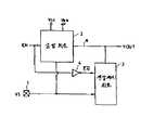
제1도는 본 발명의 전압제어회로가 내장된 반도체 집적회로, 예컨대 불휘발성 메모리의 일부를 도시해 놓은 것으로, 외부로부터 전압입력단(1)을 경유해서 공급되는 전압입력(V1)으로부터 예컨대 소거용의 고전압을 발생시키기 위한 승압회로(2)의 출력측에 출력전압(Vout)의 레벨을 일정하게 제어하기 위한 전압제어회로(3)가 접속되어 있다.FIG. 1 shows a part of a semiconductor integrated circuit, for example, a nonvolatile memory, in which the voltage control circuit of the present invention is incorporated, for example, for erasing from a voltage input V1 supplied via a
또, 제1도중 참조부호 Vcc는 통상의 전원전압, Vss는 접지단위, EN은 활성화제어신호, 4는 이 활성화제어신호(EN)를 반전시켜 전압제어회로(3)에 활성화제어신호(/EN ; 여기서, /EN은 EN의 반전신호를 의미함)을 공급하는 인버터이다.In the first diagram, Vcc denotes a normal power supply voltage, Vss denotes a ground unit, EN denotes an activation control signal, and 4 reverses the activation control signal EN so that the voltage control circuit 3 activates an activation control signal (/ EN). Where / EN is the inverted signal of EN).
이 전압제어회로(3)는 예컨대 제2도에 나타낸 바와 같이 인헨스먼트형 P채널 MOS 트랜지스터군으로 구성되어 있다. 즉, 제어대상인 전압발생회로의 전압출력단과 기준전위단[즉, 승압회로(2)의 전압출력단(a)과 전압입력단(1)]과의 사이에 각각 소오스·기판이 서로 접속됨과 더불어 각각 게이트·드레인이 서로 접속되면서 직렬접속된 복수개의 P채널 MOS 트랜지스터[P2~P(n-1)가 접속되어 있다.This voltage control circuit 3 is composed of an enhancement type P-channel MOS transistor group, for example, as shown in FIG. That is, the source and the substrate are connected to each other between the voltage output terminal of the voltage generating circuit to be controlled and the reference potential terminal (that is, the voltage output terminal a and the
여기서, P채널형 MOSFET의 게이트전극과 드레인전극을 접속하는 이유는 P채널형 MOSFET를 저항으로서 사용하기 위함이다. 당연히 종래의 N채널형 MOSFET에서는 게이트전극과 소오스전극의 접속으로 되어 있었던 것이 본원의 P채널형 MO SFET에서는 게이트전극과 드레인전극과의 접속으로 되는 것을 MOSFET의 N채널형과 P채널형의 극성이 반대이기 때문이다.Here, the reason for connecting the gate electrode and the drain electrode of the P-channel MOSFET is to use the P-channel MOSFET as a resistor. Naturally, in the conventional N-channel MOSFET, the gate electrode and the source electrode are connected. In the P-channel MO SFET of the present application, the gate electrode and the drain electrode are connected. Because it is the opposite.
그리고, 승압회로(2)의 전압출력단(a)과 상기 직렬접속된 복수개의 P채널 MO S 트랜지스터[P2~P(n-1)]의 일단측[P채널 MOS 트랜지스터(P2)의 소오스·기판상호접속점]의 사이에 소오스·기판이 서로 접속됨과 더불어 게이트에 활성화제어신호(/EN)가 공급되는 1개의 P채널 MOS 트랜지스터(P1)의 소오스·드레인간이 삽입되어 있다.Then, the source board of the voltage output terminal a of the boosting circuit 2 and one end of the plurality of P-channel MO S transistors P2 to P (n-1) connected in series (the P-channel MOS transistor P2). The source and drain of one P-channel MOS transistor P1 to which the source and substrate are connected to each other and to which the activation control signal / EN is supplied to the gate are inserted between the interconnection points.
또, 상기 직렬 접속된 복수개의 P채널 MOS 트랜지스터[P2~P1(n-1)]의 다른단측{P채널 MOS 트랜지스터[P(n-1)]의 게이트·드레인상호접속점}과 승압회로(2 )의 전압입력단(1)의 사이에 기판·게이트·드레인이 서로 접속된 1개의 P채널 MOS 트랜지스터(Pn ; 또는 1개의 다이오드이어도 좋다)가 삽입되어 있다.The other end side of the plurality of P-channel MOS transistors P2 to P1 (n-1) connected in series (gate / drain interconnection point of the P-channel MOS transistor P (n-1)) and the booster circuit 2 One P-channel MOS transistor Pn (or one diode) may be inserted between the
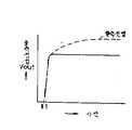
다음으로, 이 전압제어회로(3)의 동작에 대해서 제3도를 참조해서 설명한다.Next, the operation of the voltage control circuit 3 will be described with reference to FIG.
먼저, 활성화제어신호(EN)가 비활성상태, 즉 활성화제어신호(EN)가 로우레벨 ("L")이고, 그 반전신호(/EN)가 하이레벨("H')일때에는 승압회로(2)가 비동작상태이고, P채널 MOS 트랜지스터(P1)는 오프상태이며, 전압제어회로(3)는 오프상태이다.First, when the activation control signal EN is inactive, that is, the activation control signal EN is at a low level ("L") and its inversion signal / EN is at a high level ("H '), the boosting circuit 2 Is in an inoperative state, the P-channel MOS transistor P1 is in an off state, and the voltage control circuit 3 is in an off state.
이어, 시각 t1에서 활성화신호(EN)가 활성상태로 되면, 승압회로(2)가 활성화됨과 동시에 P채널 MOS 트랜지스터(P1)도 온된다. 따라서, 승압회로(2)의 승압출력은 도시된 점선과 같이 서서히 상승되지만 출력전압(Vout)은 전압제어회로(3)에 의해 거의 일정레벨로 제어된다. 여기서, 전압입력단(1)의 전압을 V1,P채널 MOS 트랜지스터(Pn)의 PN 접합다이오드의 순방향전압을 VF,P채널 MOS 트랜지스터[P1~P(n-1 )]의 각 임계치전압을 VTH로 표시하면,Subsequently, when the activation signal EN becomes active at time t1, the boosting circuit 2 is activated and the P-channel MOS transistor P1 is also turned on. Accordingly, the boosting output of the boosting circuit 2 gradually rises as shown in the dotted line, but the output voltage Vout is controlled to a substantially constant level by the voltage control circuit 3. Here, the voltage at the
Vout=V1+VF+(n-1)│VTH│Vout = V1 + VF + (n-1) │VTH │
로 된다.It becomes
또, 제4도는 출력전압(Vout)과 전압제어회로(3)의 전류사이에 관계를 도시해 놓은 것이다.4 shows the relationship between the output voltage Vout and the current of the voltage control circuit 3.
상기 전압제어회로(3)에 의하면, 복수개의 P채널 MOS 트랜지스터가 사용되므로 백게이트 바이어스 효과를 훨씬 적게 받게 된다. 따라서, 원하는 전압제어특성을 얻기 위한 P채널 MOS 트랜지스터의 접속단의 수를 용이하게 설정할 수 있게 되어 전압제어특성의 신뢰성이 향상된다.According to the voltage control circuit 3, since a plurality of P-channel MOS transistors are used, the back gate bias effect is much less. Therefore, the number of connection terminals of the P-channel MOS transistors for obtaining the desired voltage control characteristics can be easily set, thereby improving the reliability of the voltage control characteristics.
또, 상기 전압제어회로(3)는 승압회로(2)로부터 고전압이 급격히 인가되는 경우에는 그 고전압이 직접 소오스에 인가되는 P채널 MOS 트랜지스터가(P1)는 온되어 있게 되므로 그 P채널 MOS 트랜지스터(P1)는 신뢰성이 저하되지 않게 된다. 따라서 전압제어특성이 열화되어 전압제어가 불가능하게 되는 문제점이 생기지 않게 됨으로써 이 전압제어회로(3)가 삽입된 집적회로의 신뢰성이 손상받지 않게 된다.In the voltage control circuit 3, when a high voltage is suddenly applied from the boosting circuit 2, the P-channel MOS transistor P1 to which the high voltage is directly applied to the source is turned on. P1) is not deteriorated in reliability. Therefore, the problem that the voltage control characteristic is deteriorated and voltage control becomes impossible is not caused, so that the reliability of the integrated circuit into which the voltage control circuit 3 is inserted is not impaired.
더욱이, 승압회로(2)로부터 전압이 입력되지 않을 때에는 P채널 MOS 트랜지스터(P1)가 오프되므로 전압제어회로(3)에는 직류전류가 흐르지 않게 되는 바, 이에 따라 불필요한 소비전류가 생기지 않게 된다.Further, when no voltage is input from the boosting circuit 2, the P-channel MOS transistor P1 is turned off, so that no direct current flows in the voltage control circuit 3, so that unnecessary consumption current is not generated.
또, 상기 전압제어회로(3)는 테스트시 등에 전압입력단(1)의 전위가 승압회로( 2)의 전압출력단(a)의 전위보다 높게 되더라도, P채널 MOS 트랜지스터(Pn)의 PN 접합다이오드의 존재에 의해 전압입력단(1)측으로부터 전압출력단(a)측으로 흐르는 역방향 전류가 저지되게 되므로 불필요한 직류전류가 흐르지 않게 된다.In addition, the voltage control circuit 3 is used for the PN junction diode of the P-channel MOS transistor Pn even when the potential of the
제5도는 상기한 전압제어회로(3)에 있어서, P채널 MOS 트랜지스터(Pn) 및 여기에 접속되어 있는 P채널 MOS 트랜지스터[(Pn-1)]부를 취출해서 그 단면구조를 나타낸 것으로, 도면에서 참조부호 50은 P형 반도체기판, 51은 N웰, 52는 소오스용의 P+형 불순물영역, 53은 드레인용의 P+형 불순물영역, 54는 게이트전극, 55는 N+형 웰전극, 56은 배선이다. 이 도면으로부터 알 수 있는 바와 같이, 전압입력단(1)에 기판 (N웰)·게이트·드레인이 서로 접속되어 있는 P채널 MOS 트랜지스터(Pn)에는 그 소오스·기판간에 PN접합다이오드(57)가 형성되게 되므로 전압입력단(1)으로부터의 전류가 역류하는 것을 저지할 수 있게 된다.FIG. 5 shows the cross-sectional structure of the P-channel MOS transistor Pn and the P-channel MOS transistor [(Pn-1)] connected thereto in the voltage control circuit 3 described above.
여기서, N채널을 P채널로 바꿈으로써 백게이트 바이어스 효과를 받지 않게 되는 이유를 설명하면 다음과 같다.Here, the reason for not receiving the backgate bias effect by changing the N channel to the P channel is as follows.
종래 기술로서 도시된 제7도의 회로는 게이트전극과 소오스전극이 접속된 N채널형 MOSFET의 직렬 접속회로를 나타내고 있는 것으로, 게이트전극과 소오스전극이 접속되어 있는 것은 임계친전압(Vth)분의 전압강하를 갖는 저항으로서 각 N채널형 M OSFET가 사용되기 때문이다. 즉, 제7도의 회로의 V1의 전위에 대해 Vout에는 6배의 Vth분 만큼 높은 전위가 얻어지게 된다(이것이 종래 회로의 기능임).The circuit of FIG. 7 shown as a prior art shows a series connection circuit of an N-channel MOSFET in which a gate electrode and a source electrode are connected, and the gate electrode and the source electrode are connected to a threshold voltage (Vth). This is because each N-channel M OSFET is used as a resistor having a drop. That is, a potential as high as six times Vth is obtained for Vout relative to the potential of V1 of the circuit of FIG. 7 (this is a function of the conventional circuit).
그런데, 종래 회로에서 백게이트 바이어스 효과를 억제하기 위해서는 각 N채널형 MOSFET의 소오스영역과 채널영역의 전위를 동일하게 설정하지 않으면 안되는데 , 이와 같은 필요성에 대해 종래 회로는 모순을 갖추고 있다. 이는, 각 N채널형 MOSFET의 소오스영역 및 드레인영역이 동일한 반도체기판중에 형성되어 있기 때문에 채널영역의 전위가 모두 동일하게 되어 버리기 때문이다. 각 N채널형 MOSFET의 소오스영역(게이트전극과 소오스전극이 접속되어 있는)의 전위를 채널영역의 전위와 동일하게 되도록 접속하면, 각 N채널형 MOSFET가 임계친전압(Vth)분의 전압강하를 갖는 저항으로서 기능하지 않아 상기한 V1과 Vout의 관계를 얻을 수 없게 된다.By the way, in order to suppress the back gate bias effect in the conventional circuit, the source and channel region potentials of the respective N-channel MOSFETs must be set equal. However, the conventional circuit has a contradiction. This is because the source region and the drain region of each N-channel MOSFET are formed in the same semiconductor substrate, so that the potentials of the channel regions become the same. When the potential of the source region (where the gate electrode and the source electrode are connected) of each N-channel MOSFET is connected to be the same as that of the channel region, the respective N-channel MOSFET reduces the voltage drop for the threshold electrostatic voltage (Vth). It does not function as a resistor having such a relationship that V1 and Vout cannot be obtained.
여기서, 본원 발명에서는 백게이트 바이어스 효과를 억제하기 위해 필요한 소오스영역과 채널영역의 동전위화가 도모되는 구조의 N채널형 MOSFET에 주목한다. N채널형 MOSFET는 통상의 P형 반도체기판에 N형 웰영역을 형성하고, 그 중에 소오스영역 및 드레인영역을 형성하는 것으로, 따라서 개개의 N채널형 MOSFET가 형성되는 N형 웰영역을 분리하여 두면, 채널영역의 전위가 모두 동일하게 되어버리는 결함이 발생하지 않게 되는 것이다.Here, in the present invention, attention is directed to an N-channel MOSFET having a structure in which the source region and the channel region are required to counteract the back gate bias effect. The N-channel MOSFET forms an N-type well region in a conventional P-type semiconductor substrate, and forms a source region and a drain region therein. Therefore, when the N-type well region in which individual N-channel MOSFETs are formed is separated, Therefore, the defect that the potentials of the channel regions are all the same does not occur.
또, 상기 실시예의 P채널 MOS 트랜지스터(P1)는 필요에 따라 생략해도 되고, 마찬가지로 P채널 MOS 트랜지스터(Pn)도 필요에 따라 생략해도 된다.In addition, the P-channel MOS transistor P1 of the said embodiment may be omitted as needed, and similarly, the P-channel MOS transistor Pn may be omitted as needed.
한편, 본원 청구범위의 각 구성요소에 병기된 도면참조부호는 본원 발명의 이해를 용이하게 하기 위한 것으로, 본원 발명의 기술적 범위를 도면에 도시한 실시예로 한정할 의도에서 병기한 것은 아니다.On the other hand, reference numerals denoted in the components of the claims of the present application to facilitate the understanding of the present invention, not intended to limit the technical scope of the present invention to the embodiments shown in the drawings.
[발명의 효과][Effects of the Invention]
상기한 바와 같은 본 발명에 의하면, 원하는 전압제어특성을 얻기 위한 MOS 트랜지스터의 접속단의 수를 용이하게 결정할 수 있게 되므로 전압제어특성의 신뢰성이 향상된 전압제어회로를 실현할 수 있게 된다.According to the present invention as described above, it is possible to easily determine the number of connection terminals of the MOS transistor for obtaining the desired voltage control characteristic, thereby realizing a voltage control circuit with improved reliability of the voltage control characteristic.
또 본 발명에 의하면, 제어대상인 전압발생회로로부터 고전압이 급격히 인가되어도 이 고전압에 의해 MOS 트랜지스터의 신뢰성이 저하되는 것을 방지할 수 있게 되고, 더욱이 상기 전압발생회로로부터 전압이 입력되지 않을 때에는 직류전류에 의한 불필요한 소비전류를 방지할 수 있도록 된 전압제어회로를 실현할 수 있게 된다.According to the present invention, even when a high voltage is suddenly applied from the voltage generation circuit to be controlled, the reliability of the MOS transistor can be prevented from being deteriorated by this high voltage. Furthermore, when a voltage is not input from the voltage generation circuit, It is possible to realize the voltage control circuit which can prevent unnecessary current consumption by the electronic device.
또, 본 발명에 의하면, 테스트시 등에 제어대상인 전압제어회로의 기준전위측의 출력단의 전위가 이 전압 발생회로의 전압출력단의 전위보다 높게 되더라도 불필요한 직류전류의 흐름이 방지되도록 된 전압제어회로를 실현할 수 있게 된다.Further, according to the present invention, even when the potential of the output terminal on the reference potential side of the voltage control circuit to be controlled is higher than the potential of the voltage output terminal of the voltage generating circuit during the test or the like, it is possible to realize the voltage control circuit which prevents unnecessary DC current flow. It becomes possible.
Claims (3)
Translated fromKoreanApplications Claiming Priority (2)
| Application Number | Priority Date | Filing Date | Title |
|---|---|---|---|
| JP01-036479 | 1989-02-16 | ||
| JP1036479AJPH02215154A (en) | 1989-02-16 | 1989-02-16 | Voltage control circuit |
Publications (2)
| Publication Number | Publication Date |
|---|---|
| KR900013380A KR900013380A (en) | 1990-09-05 |
| KR940001251B1true KR940001251B1 (en) | 1994-02-18 |
Family
ID=12470952
Family Applications (1)
| Application Number | Title | Priority Date | Filing Date |
|---|---|---|---|
| KR1019900001909AExpired - Fee RelatedKR940001251B1 (en) | 1989-02-16 | 1990-02-16 | Voltage control circuit |
Country Status (5)
| Country | Link |
|---|---|
| US (1) | US5029282A (en) |
| EP (1) | EP0382929B1 (en) |
| JP (1) | JPH02215154A (en) |
| KR (1) | KR940001251B1 (en) |
| DE (1) | DE68917900T2 (en) |
Families Citing this family (84)
| Publication number | Priority date | Publication date | Assignee | Title |
|---|---|---|---|---|
| JPH0470204A (en)* | 1990-07-11 | 1992-03-05 | Sony Corp | Bias voltage generation circuit and operational amplifier |
| JPH04205994A (en)* | 1990-11-30 | 1992-07-28 | Toshiba Corp | Precharge circuit |
| US5126590A (en)* | 1991-06-17 | 1992-06-30 | Micron Technology, Inc. | High efficiency charge pump |
| FR2681180B1 (en)* | 1991-09-05 | 1996-10-25 | Gemplus Card Int | PROGRAMMING VOLTAGE REGULATION CIRCUIT FOR PROGRAMMABLE MEMORIES. |
| DE4130191C2 (en)* | 1991-09-30 | 1993-10-21 | Samsung Electronics Co Ltd | Constant voltage generator for a semiconductor device with cascaded charging or discharging circuit |
| KR940005691B1 (en)* | 1991-10-25 | 1994-06-22 | 삼성전자 주식회사 | Charge pumping circuit of the substrate-voltage generating device |
| CN1075690C (en)* | 1991-11-07 | 2001-11-28 | 摩托罗拉公司 | Mixed signal processing system and method for powering same |
| EP0961290B1 (en)* | 1991-12-09 | 2001-11-14 | Fujitsu Limited | Flash memory with improved erasability and its circuitry |
| US5260646A (en)* | 1991-12-23 | 1993-11-09 | Micron Technology, Inc. | Low power regulator for a voltage generator circuit |
| US5191232A (en)* | 1992-03-17 | 1993-03-02 | Silicon Storage Technology, Inc. | High frequency voltage multiplier for an electrically erasable and programmable memory device |
| US5291446A (en)* | 1992-10-22 | 1994-03-01 | Advanced Micro Devices, Inc. | VPP power supply having a regulator circuit for controlling a regulated positive potential |
| JP3420606B2 (en)* | 1993-03-15 | 2003-06-30 | 株式会社東芝 | High voltage generator |
| JP3043201B2 (en)* | 1993-04-22 | 2000-05-22 | 株式会社東芝 | Boost circuit |
| US5811990A (en) | 1993-10-15 | 1998-09-22 | Micron Technology, Inc. | Voltage pump and a level translator circuit |
| US5642073A (en)* | 1993-12-06 | 1997-06-24 | Micron Technology, Inc. | System powered with inter-coupled charge pumps |
| JP3159586B2 (en)* | 1993-12-09 | 2001-04-23 | 株式会社東芝 | Boost circuit device |
| FR2717918B1 (en)* | 1994-03-25 | 1996-05-24 | Suisse Electronique Microtech | Circuit to control the voltages between box and sources of mos transistors and servo system of the relationship between the dynamic and static currents of a mos logic circuit. |
| TW271011B (en)* | 1994-04-20 | 1996-02-21 | Nippon Steel Corp | |
| FR2719135B1 (en)* | 1994-04-21 | 1996-06-28 | Sgs Thomson Microelectronics | Voltage limiting circuit with hysteresis comparator. |
| US6140861A (en)* | 1994-06-27 | 2000-10-31 | Texas Instruments Incorporated | Bias pump arrangement including a signal-transition-detection circuit |
| US5513225A (en)* | 1994-08-31 | 1996-04-30 | International Business Machines Corporation | Resistorless phase locked loop circuit employing direct current injection |
| US5491439A (en)* | 1994-08-31 | 1996-02-13 | International Business Machines Corporation | Method and apparatus for reducing jitter in a phase locked loop circuit |
| US5525932A (en)* | 1994-08-31 | 1996-06-11 | International Business Machines Corporation | Lock indicator for phase locked loop circuit |
| US5495207A (en)* | 1994-08-31 | 1996-02-27 | International Business Machines Corporation | Differential current controlled oscillator with variable load |
| US5619161A (en)* | 1994-08-31 | 1997-04-08 | International Business Machines Corporation | Diffrential charge pump with integrated common mode control |
| JP2718375B2 (en)* | 1994-09-30 | 1998-02-25 | 日本電気株式会社 | Charge pump circuit |
| US5694074A (en)* | 1994-10-31 | 1997-12-02 | Mitsubishi Denki Kabushiki Kaisha | Semiconductor integrated circuit being able to generate sufficient boost potential disregarding generation of noise |
| US5541551A (en)* | 1994-12-23 | 1996-07-30 | Advinced Micro Devices, Inc. | Analog voltage reference generator system |
| KR0149220B1 (en)* | 1994-12-27 | 1998-12-01 | 김주용 | Charge pump circuit |
| FR2729014A1 (en)* | 1994-12-29 | 1996-07-05 | Gec Alsthom Transport Sa | ELECTRONIC DEVICE FOR CONVERTING ELECTRICAL ENERGY AND POWER SUPPLY USING THE SAME |
| EP0737643B1 (en)* | 1995-04-14 | 2000-09-13 | STMicroelectronics S.r.l. | Voltage generator-booster for supplying an approximately constant voltage level |
| US5973956A (en)* | 1995-07-31 | 1999-10-26 | Information Storage Devices, Inc. | Non-volatile electrically alterable semiconductor memory for analog and digital storage |
| US5907484A (en)* | 1996-04-25 | 1999-05-25 | Programmable Microelectronics Corp. | Charge pump |
| US5625544A (en)* | 1996-04-25 | 1997-04-29 | Programmable Microelectronics Corp. | Charge pump |
| US5994948A (en)* | 1997-08-27 | 1999-11-30 | Sgs-Thomson Microelectronics S.R.L. | CMOS twin-tub negative voltage switching architecture |
| US6275097B1 (en) | 1999-04-02 | 2001-08-14 | S3 Incorporated, Inc. | Differential charge pump with low voltage common mode feedback circuit |
| US6636104B2 (en)* | 2000-06-13 | 2003-10-21 | Microsemi Corporation | Multiple output charge pump |
| US6556067B2 (en)* | 2000-06-13 | 2003-04-29 | Linfinity Microelectronics | Charge pump regulator with load current control |
| US7467379B2 (en)* | 2001-01-16 | 2008-12-16 | International Business Machines Corporation | System and method for incrementally executing a client/server application |
| US6989750B2 (en)* | 2001-02-12 | 2006-01-24 | Symbol Technologies, Inc. | Radio frequency identification architecture |
| RU2211478C2 (en)* | 2001-04-25 | 2003-08-27 | Федеральный научно-производственный центр закрытое акционерное общество "Научно-производственный концерн (объединение) "ЭНЕРГИЯ" | Off-line power system |
| US6804502B2 (en) | 2001-10-10 | 2004-10-12 | Peregrine Semiconductor Corporation | Switch circuit and method of switching radio frequency signals |
| US6720822B2 (en)* | 2001-10-31 | 2004-04-13 | Stmicroelectronics S.R.L. | Negative charge pump architecture with self-generated boosted phases |
| DE10157865A1 (en)* | 2001-11-26 | 2003-06-26 | Infineon Technologies Ag | Programmable voltage pump for generating voltage has a trim input for adjusting a desired output voltage and a means for generating an overflow level at the output. |
| US6498737B1 (en)* | 2002-01-16 | 2002-12-24 | Taiwan Semiconductor Manufacturing Company | Voltage regulator with low sensitivity to body effect |
| US6788130B2 (en)* | 2002-09-25 | 2004-09-07 | Texas Instruments Incorporated | Efficient charge pump capable of high voltage operation |
| US7719343B2 (en) | 2003-09-08 | 2010-05-18 | Peregrine Semiconductor Corporation | Low noise charge pump method and apparatus |
| US7649402B1 (en)* | 2003-12-23 | 2010-01-19 | Tien-Min Chen | Feedback-controlled body-bias voltage source |
| US7119604B2 (en)* | 2004-06-17 | 2006-10-10 | Taiwan Semiconductor Manufacturing Company, Ltd. | Back-bias voltage regulator having temperature and process variation compensation and related method of regulating a back-bias voltage |
| EP3570374B1 (en) | 2004-06-23 | 2022-04-20 | pSemi Corporation | Integrated rf front end |
| US7372318B2 (en) | 2004-07-26 | 2008-05-13 | Honeywell International Inc. | Precision, low drift, stacked voltage reference |
| FR2878986B1 (en)* | 2004-12-08 | 2007-04-27 | Atmel Corp | PRINCIPLE OF POWER CONTROL OF HIGH VOLTAGE OUTPUT IN INTEGRATED CIRCUIT DEVICES |
| JP2006311731A (en)* | 2005-04-28 | 2006-11-09 | Seiko Instruments Inc | Electronic circuit |
| US9653601B2 (en) | 2005-07-11 | 2017-05-16 | Peregrine Semiconductor Corporation | Method and apparatus for use in improving linearity of MOSFETs using an accumulated charge sink-harmonic wrinkle reduction |
| US7910993B2 (en) | 2005-07-11 | 2011-03-22 | Peregrine Semiconductor Corporation | Method and apparatus for use in improving linearity of MOSFET's using an accumulated charge sink |
| USRE48965E1 (en) | 2005-07-11 | 2022-03-08 | Psemi Corporation | Method and apparatus improving gate oxide reliability by controlling accumulated charge |
| US20080076371A1 (en) | 2005-07-11 | 2008-03-27 | Alexander Dribinsky | Circuit and method for controlling charge injection in radio frequency switches |
| US7890891B2 (en) | 2005-07-11 | 2011-02-15 | Peregrine Semiconductor Corporation | Method and apparatus improving gate oxide reliability by controlling accumulated charge |
| US20070126494A1 (en)* | 2005-12-06 | 2007-06-07 | Sandisk Corporation | Charge pump having shunt diode for improved operating efficiency |
| US7372320B2 (en)* | 2005-12-16 | 2008-05-13 | Sandisk Corporation | Voltage regulation with active supplemental current for output stabilization |
| US20070139099A1 (en)* | 2005-12-16 | 2007-06-21 | Sandisk Corporation | Charge pump regulation control for improved power efficiency |
| US20070229149A1 (en)* | 2006-03-30 | 2007-10-04 | Sandisk Corporation | Voltage regulator having high voltage protection |
| US7554311B2 (en)* | 2006-07-31 | 2009-06-30 | Sandisk Corporation | Hybrid charge pump regulation |
| US7368979B2 (en) | 2006-09-19 | 2008-05-06 | Sandisk Corporation | Implementation of output floating scheme for hv charge pumps |
| WO2008086396A2 (en) | 2007-01-09 | 2008-07-17 | Power Monitors Inc. | Method and apparatus for smart circuit breaker |
| US7960772B2 (en) | 2007-04-26 | 2011-06-14 | Peregrine Semiconductor Corporation | Tuning capacitance to enhance FET stack voltage withstand |
| DE102007023652B4 (en)* | 2007-05-22 | 2013-08-14 | Austriamicrosystems Ag | Voltage regulator and voltage regulation method |
| US7586363B2 (en) | 2007-12-12 | 2009-09-08 | Sandisk Corporation | Diode connected regulation of charge pumps |
| US8169081B1 (en) | 2007-12-27 | 2012-05-01 | Volterra Semiconductor Corporation | Conductive routings in integrated circuits using under bump metallization |
| WO2009111386A2 (en) | 2008-03-04 | 2009-09-11 | Power Monitors, Inc. | Method and apparatus for a voice-prompted electrical hookup |
| US7683700B2 (en) | 2008-06-25 | 2010-03-23 | Sandisk Corporation | Techniques of ripple reduction for charge pumps |
| US9660590B2 (en) | 2008-07-18 | 2017-05-23 | Peregrine Semiconductor Corporation | Low-noise high efficiency bias generation circuits and method |
| EP2421132A2 (en)* | 2008-07-18 | 2012-02-22 | Peregrine Semiconductor Corporation | Charge pump with a plurality of transfer control switches |
| US7795952B2 (en) | 2008-12-17 | 2010-09-14 | Sandisk Corporation | Regulation of recovery rates in charge pumps |
| US8773108B2 (en) | 2009-11-10 | 2014-07-08 | Power Monitors, Inc. | System, method, and apparatus for a safe powerline communications instrumentation front-end |
| EP3324153A1 (en) | 2010-07-29 | 2018-05-23 | Power Monitors, Inc. | Method and apparatus for a demand management monitoring system |
| US10060957B2 (en) | 2010-07-29 | 2018-08-28 | Power Monitors, Inc. | Method and apparatus for a cloud-based power quality monitor |
| US9264053B2 (en) | 2011-01-18 | 2016-02-16 | Peregrine Semiconductor Corporation | Variable frequency charge pump |
| US8686787B2 (en) | 2011-05-11 | 2014-04-01 | Peregrine Semiconductor Corporation | High voltage ring pump with inverter stages and voltage boosting stages |
| US20150236748A1 (en) | 2013-03-14 | 2015-08-20 | Peregrine Semiconductor Corporation | Devices and Methods for Duplexer Loss Reduction |
| US9917507B2 (en) | 2015-05-28 | 2018-03-13 | Sandisk Technologies Llc | Dynamic clock period modulation scheme for variable charge pump load currents |
| US9647536B2 (en) | 2015-07-28 | 2017-05-09 | Sandisk Technologies Llc | High voltage generation using low voltage devices |
| US9520776B1 (en) | 2015-09-18 | 2016-12-13 | Sandisk Technologies Llc | Selective body bias for charge pump transfer switches |
| CN105404346B (en)* | 2015-12-22 | 2017-08-08 | 上海华虹宏力半导体制造有限公司 | Voltage adjustment, high pressure are produced and memory circuitry |
Family Cites Families (13)
| Publication number | Priority date | Publication date | Assignee | Title |
|---|---|---|---|---|
| JPS5421249A (en)* | 1977-07-19 | 1979-02-17 | Mitsubishi Electric Corp | Logic circuit |
| JPS5434044A (en)* | 1977-08-19 | 1979-03-13 | Seiko Instr & Electronics Ltd | Constant voltage circuit |
| JPS5632758A (en)* | 1979-08-27 | 1981-04-02 | Fujitsu Ltd | Substrate bias generating circuit |
| JPS5717227A (en)* | 1980-07-04 | 1982-01-28 | Hitachi Ltd | Integrated circuit device |
| US4439692A (en)* | 1981-12-07 | 1984-03-27 | Signetics Corporation | Feedback-controlled substrate bias generator |
| US4553047A (en)* | 1983-01-06 | 1985-11-12 | International Business Machines Corporation | Regulator for substrate voltage generator |
| US4631421A (en)* | 1984-08-14 | 1986-12-23 | Texas Instruments | CMOS substrate bias generator |
| JPS6159688A (en)* | 1984-08-31 | 1986-03-27 | Hitachi Ltd | Semiconductor integrated circuit device |
| JPS6212148A (en)* | 1985-07-10 | 1987-01-21 | Fujitsu Ltd | Semiconductor integrated circuit device |
| JPS62188255A (en)* | 1986-02-13 | 1987-08-17 | Toshiba Corp | Reference voltage generating circuit |
| KR890005159B1 (en)* | 1987-04-30 | 1989-12-14 | 삼성전자 주식회사 | Back Bias Voltage Generator |
| US4837459A (en)* | 1987-07-13 | 1989-06-06 | International Business Machines Corp. | CMOS reference voltage generation |
| US4961167A (en)* | 1988-08-26 | 1990-10-02 | Mitsubishi Denki Kabushiki Kaisha | Substrate bias generator in a dynamic random access memory with auto/self refresh functions and a method of generating a substrate bias therein |
- 1989
- 1989-02-16JPJP1036479Apatent/JPH02215154A/enactivePending
- 1989-12-14USUS07/450,569patent/US5029282A/ennot_activeExpired - Lifetime
- 1989-12-15DEDE68917900Tpatent/DE68917900T2/ennot_activeExpired - Fee Related
- 1989-12-15EPEP89123228Apatent/EP0382929B1/ennot_activeExpired - Lifetime
- 1990
- 1990-02-16KRKR1019900001909Apatent/KR940001251B1/ennot_activeExpired - Fee Related
Also Published As
| Publication number | Publication date |
|---|---|
| KR900013380A (en) | 1990-09-05 |
| EP0382929A3 (en) | 1990-09-26 |
| US5029282A (en) | 1991-07-02 |
| EP0382929A2 (en) | 1990-08-22 |
| DE68917900T2 (en) | 1995-02-02 |
| JPH02215154A (en) | 1990-08-28 |
| DE68917900D1 (en) | 1994-10-06 |
| EP0382929B1 (en) | 1994-08-31 |
Similar Documents
| Publication | Publication Date | Title |
|---|---|---|
| KR940001251B1 (en) | Voltage control circuit | |
| KR890004958B1 (en) | Semiconductor integrated circuit | |
| JP2616142B2 (en) | Output circuit | |
| KR930004177B1 (en) | Semiconductor memory device | |
| US4952825A (en) | Semiconductor integrated circuit having signal level conversion circuit | |
| US6320414B1 (en) | High-voltage level tolerant transistor circuit | |
| KR100243850B1 (en) | High Voltage Level Shifter for High Voltage Switching in Nonvolatile Memory Integrated Circuits | |
| KR910001380B1 (en) | Power switching circuit | |
| US5270589A (en) | Input/output buffer circuit for semiconductor integrated circuit | |
| US6285213B1 (en) | Semiconductor integrated circuit device | |
| JPS60500433A (en) | Substrate bias control circuit and method | |
| KR0122246Y1 (en) | Level conversion circuit | |
| KR100318298B1 (en) | Semiconductor device | |
| KR900004012A (en) | Semiconductor integrated circuit device and its combination electronic device | |
| JPH08272467A (en) | Substrate potential generation circuit | |
| KR100211758B1 (en) | Multi-power data buffer | |
| EP0713167A1 (en) | A voltage level converter | |
| KR100357279B1 (en) | Pull-up circuit and semiconductor device using the same | |
| JPH07220484A (en) | Voltage converter | |
| US5786719A (en) | Mode setting circuit and mode setting apparatus used to select a particular semiconductor function | |
| US6476641B2 (en) | Low power consuming circuit | |
| US6472924B1 (en) | Integrated semiconductor circuit having analog and logic circuits | |
| KR100196609B1 (en) | Semiconductor device having supply voltage converting circuits | |
| US6184715B1 (en) | Bus-hold input circuit adapted for receiving input signals with voltage levels higher than the voltage supply thereof | |
| JP2699828B2 (en) | Input/output circuit of semiconductor device |
Legal Events
| Date | Code | Title | Description |
|---|---|---|---|
| A201 | Request for examination | ||
| PA0109 | Patent application | St.27 status event code:A-0-1-A10-A12-nap-PA0109 | |
| PA0201 | Request for examination | St.27 status event code:A-1-2-D10-D11-exm-PA0201 | |
| R17-X000 | Change to representative recorded | St.27 status event code:A-3-3-R10-R17-oth-X000 | |
| PG1501 | Laying open of application | St.27 status event code:A-1-1-Q10-Q12-nap-PG1501 | |
| E902 | Notification of reason for refusal | ||
| PE0902 | Notice of grounds for rejection | St.27 status event code:A-1-2-D10-D21-exm-PE0902 | |
| T11-X000 | Administrative time limit extension requested | St.27 status event code:U-3-3-T10-T11-oth-X000 | |
| T11-X000 | Administrative time limit extension requested | St.27 status event code:U-3-3-T10-T11-oth-X000 | |
| T11-X000 | Administrative time limit extension requested | St.27 status event code:U-3-3-T10-T11-oth-X000 | |
| T11-X000 | Administrative time limit extension requested | St.27 status event code:U-3-3-T10-T11-oth-X000 | |
| P11-X000 | Amendment of application requested | St.27 status event code:A-2-2-P10-P11-nap-X000 | |
| P13-X000 | Application amended | St.27 status event code:A-2-2-P10-P13-nap-X000 | |
| G160 | Decision to publish patent application | ||
| PG1605 | Publication of application before grant of patent | St.27 status event code:A-2-2-Q10-Q13-nap-PG1605 | |
| E701 | Decision to grant or registration of patent right | ||
| PE0701 | Decision of registration | St.27 status event code:A-1-2-D10-D22-exm-PE0701 | |
| GRNT | Written decision to grant | ||
| PR0701 | Registration of establishment | St.27 status event code:A-2-4-F10-F11-exm-PR0701 | |
| PR1002 | Payment of registration fee | St.27 status event code:A-2-2-U10-U11-oth-PR1002 Fee payment year number:1 | |
| PR1001 | Payment of annual fee | St.27 status event code:A-4-4-U10-U11-oth-PR1001 Fee payment year number:4 | |
| PR1001 | Payment of annual fee | St.27 status event code:A-4-4-U10-U11-oth-PR1001 Fee payment year number:5 | |
| R18-X000 | Changes to party contact information recorded | St.27 status event code:A-5-5-R10-R18-oth-X000 | |
| PN2301 | Change of applicant | St.27 status event code:A-5-5-R10-R13-asn-PN2301 St.27 status event code:A-5-5-R10-R11-asn-PN2301 | |
| PR1001 | Payment of annual fee | St.27 status event code:A-4-4-U10-U11-oth-PR1001 Fee payment year number:6 | |
| R18-X000 | Changes to party contact information recorded | St.27 status event code:A-5-5-R10-R18-oth-X000 | |
| R18-X000 | Changes to party contact information recorded | St.27 status event code:A-5-5-R10-R18-oth-X000 | |
| PR1001 | Payment of annual fee | St.27 status event code:A-4-4-U10-U11-oth-PR1001 Fee payment year number:7 | |
| PR1001 | Payment of annual fee | St.27 status event code:A-4-4-U10-U11-oth-PR1001 Fee payment year number:8 | |
| R18-X000 | Changes to party contact information recorded | St.27 status event code:A-5-5-R10-R18-oth-X000 | |
| PR1001 | Payment of annual fee | St.27 status event code:A-4-4-U10-U11-oth-PR1001 Fee payment year number:9 | |
| FPAY | Annual fee payment | Payment date:20030130 Year of fee payment:10 | |
| PR1001 | Payment of annual fee | St.27 status event code:A-4-4-U10-U11-oth-PR1001 Fee payment year number:10 | |
| LAPS | Lapse due to unpaid annual fee | ||
| PC1903 | Unpaid annual fee | St.27 status event code:A-4-4-U10-U13-oth-PC1903 Not in force date:20040219 Payment event data comment text:Termination Category : DEFAULT_OF_REGISTRATION_FEE | |
| PC1903 | Unpaid annual fee | St.27 status event code:N-4-6-H10-H13-oth-PC1903 Ip right cessation event data comment text:Termination Category : DEFAULT_OF_REGISTRATION_FEE Not in force date:20040219 | |
| P22-X000 | Classification modified | St.27 status event code:A-4-4-P10-P22-nap-X000 | |
| P22-X000 | Classification modified | St.27 status event code:A-4-4-P10-P22-nap-X000 | |
| R18-X000 | Changes to party contact information recorded | St.27 status event code:A-5-5-R10-R18-oth-X000 |