KR920010974B1 - Self configuring memory system - Google Patents
Self configuring memory systemDownload PDFInfo
- Publication number
- KR920010974B1 KR920010974B1KR1019880015413AKR880015413AKR920010974B1KR 920010974 B1KR920010974 B1KR 920010974B1KR 1019880015413 AKR1019880015413 AKR 1019880015413AKR 880015413 AKR880015413 AKR 880015413AKR 920010974 B1KR920010974 B1KR 920010974B1
- Authority
- KR
- South Korea
- Prior art keywords
- memory
- digital
- signal
- cpu
- value
- Prior art date
- Legal status (The legal status is an assumption and is not a legal conclusion. Google has not performed a legal analysis and makes no representation as to the accuracy of the status listed.)
- Expired
Links
Images

Classifications
- G—PHYSICS
- G06—COMPUTING OR CALCULATING; COUNTING
- G06F—ELECTRIC DIGITAL DATA PROCESSING
- G06F13/00—Interconnection of, or transfer of information or other signals between, memories, input/output devices or central processing units
- G—PHYSICS
- G06—COMPUTING OR CALCULATING; COUNTING
- G06F—ELECTRIC DIGITAL DATA PROCESSING
- G06F12/00—Accessing, addressing or allocating within memory systems or architectures
- G06F12/02—Addressing or allocation; Relocation
- G06F12/06—Addressing a physical block of locations, e.g. base addressing, module addressing, memory dedication
- G06F12/0646—Configuration or reconfiguration
- G06F12/0684—Configuration or reconfiguration with feedback, e.g. presence or absence of unit detected by addressing, overflow detection
Landscapes
- Engineering & Computer Science (AREA)
- Theoretical Computer Science (AREA)
- Physics & Mathematics (AREA)
- General Engineering & Computer Science (AREA)
- General Physics & Mathematics (AREA)
- Techniques For Improving Reliability Of Storages (AREA)
- Memory System (AREA)
Abstract
Translated fromKoreanDescription
Translated fromKorean제1도는 본 발명을 합체한 마이크로컴퓨터의 블록도.1 is a block diagram of a microcomputer incorporating the present invention.
제2도는 본 발명의 메모리 보드에 의해 활용되는 개시 어드레스 신호를 정의하는 표.2 is a table defining start address signals utilized by the memory board of the present invention.
제3도는 본 발명의 메모리 보드에 의해 공급된 메모리 인식신호를 정의하는 표.3 is a table that defines a memory recognition signal supplied by the memory board of the present invention.
제4도는 본 발명의 메모리 보드에 대한 블록도.4 is a block diagram of a memory board of the present invention.
본 발명은 마이크로컴퓨터 메모리 시스템에 관한 것으로서, 특히 메모리 용량에 관한 자기 형성시스템에 관한 것이다.FIELD OF THE INVENTION The present invention relates to microcomputer memory systems, and more particularly to a self-forming system relating to memory capacity.
현 마이크로컴퓨터 시스템은 일반적으로 확장형 내부메모리를 가지고 있다. 예를 들어, 마이크로컴퓨터 샤시내에 통상적으로 메모리 보드가 삽입되는 “확장슬롯”을 가지고 있다. 이러한 메모리 보드는 일반적으로 반도체 메모리 칩이 배열된 인쇄회로카드이다. 마이크로컴퓨터의 중앙처리장치(CPU)가 이러한 확장가능한 메모리에 데이터를 저장하고 검색하기 위하여, CPU는 가능한 메모리의 전체용량을 알아야 한다. 게다가, 전체메모리 공간은 어드레스 지정에 불명료함이 없이 구성되어야 한다.Current microcomputer systems generally have expandable internal memory. For example, they have an "expansion slot" into which a memory board is typically inserted in a microcomputer chassis. Such a memory board is generally a printed circuit card in which semiconductor memory chips are arranged. In order for the microcomputer's central processing unit (CPU) to store and retrieve data in this expandable memory, the CPU must know the total amount of available memory. In addition, the entire memory space must be configured without ambiguity in addressing.
확장가능한 메모리를 가진 대부분의 마이크로컴퓨터에서, 컴퓨터 내부의 일세트의 스위치들은 메모리 모듈이 삽입 또는 제거될때마다 메모리 용량을 표시하도록 설정되어져야 한다. 메모리 용량을 바꾸거나 스위치가 잘못된 위치로 설정될 때 기술자가 스위치 설정을 잊어버리는 것이 일반적이다. 둘중 어느경우에서는, CPU는 메모리용량에 대한 잘못된 정보를 수신하고, 순차적으로 컴퓨터는 메모리를 적당하게 어드레스지정하는 것이 불가능하게 될 것이다. 또다른 문제로는, 사용자가 메모리카드를 장착하여 스위치를 잘못 세트시키면 여분의 메모리 용량에 대한 잇점을 얻을 수 없다는 것이다.In most microcomputers with expandable memory, a set of switches inside the computer should be set to indicate the memory capacity each time a memory module is inserted or removed. It is common for a technician to forget the switch setting when changing memory capacity or when the switch is set to the wrong position. In either case, the CPU will receive incorrect information about the memory capacity, and in turn the computer will be unable to properly address the memory. Another problem is that if the user inserts a memory card and sets the switch incorrectly, the benefit of the extra memory capacity is not available.
다른 어떤 시스템에서는, CPU가 메모리 모듈의 존재를 감지한다. 이것은 일반적으로 소정의 메모리 옵션이 설치되었는지를 결정하는데만 한정된다. 그러한 시스템은 일 이상의 여러 슬롯에 삽입되는 임의의 크기의 메모리 모듈을 수용할 수 없다.In some other systems, the CPU detects the presence of a memory module. This is generally limited only to determining whether certain memory options have been installed. Such a system cannot accommodate a memory module of any size inserted into one or more of several slots.
차후에 설명되는 것처럼, 본 발명은 다양한 기억용량의 메모리 모듈이 일 이상의 여러 확장 슬롯에 삽입되는 충분한 자기형성메모리를 제공한다. CPU와 메모리 모듈간에 통과되는 신호는 그들의 적당한 개시 어드레스를 메모리 모듈에게 알린다.As will be explained later, the present invention provides a sufficient self-forming memory in which memory modules of various storage capacities are inserted into one or more expansion slots. The signals passed between the CPU and the memory module inform the memory modules of their proper starting address.
본 발명은 중앙처리장치(CPU)를 포함하고 확장 메모리 슬롯이 있는 샤시를 구비하는 컴퓨터 시스템에 자기형성 메모리를 제공한다. 메모리는 CPU와 물리적으로 합체된 메모리와 샤시내의 확장 슬롯에 선택적으로 삽입가능한 다수의 확장메모리보드에 들어있는 부가적인 메모리간에 분포되어 있다. CPU 메모리와 확장 메모리는 각각 다양한 독립적 구성을 갖는다. 시스템 내에 장착된 것이 있다면 CPU는 CPU메모리로부터 시작하며 연속적인 확장 메모리 보드의 메모리 공간을 통하여 연속되는 단일의 인접 메모리공간이 있는 것처럼 동작한다.The present invention provides a self-forming memory in a computer system including a central processing unit (CPU) and having a chassis with an expansion memory slot. Memory is distributed between the memory physically associated with the CPU and the additional memory contained in a number of expansion memory boards that can be selectively inserted into expansion slots in the chassis. The CPU memory and the expansion memory each have various independent configurations. If there is something in the system, the CPU starts from the CPU memory and operates as if there is a single contiguous contiguous memory space through the contiguous expansion memory board memory space.
CPU는 보드상의 메모리와 확장메모리 보드에 그들 메모리의 용량을 지시하는 신호를 각각 공급한다. 각각의 확장메모리보드 상의 논리회로는 CPU 메모리의 용량을 지시하는 신호와 바로 그 확장메모리 보드에 장착된 메모리 용량을 지시하는 신호를 수신한다. 그후 각 보드상의 논리회로는 CPU 메모리, CPU 메모리와 확장메모리 보드간의 확장메모리, 및 보드상에 내재하는 메모리를 구성하는 전체 메모리를 계산한다. 그후 이값은 데이지 화한(daisy chain) 식으로 인접 확장메모리 보드로 패스된다.The CPU supplies signals on the board to the memory and the expansion memory board, respectively, indicating the capacity of those memories. Logic circuits on each expansion memory board receive a signal indicating the capacity of the CPU memory and a signal indicating the memory capacity mounted on the expansion memory board. The logic circuits on each board then calculate the total memory constituting the CPU memory, the expansion memory between the CPU memory and the expansion memory board, and the memory inherent on the board. This value is then daisy chained to adjacent expansion memory boards.
또한 각각의 확장 메모리 보드상의 논리회로는 보드상에 내재하는 물리적인 메모리 공간에 대응하는 어드레스범위를 결정한다. 그 범위내의 어드레스가 CPU에 의해 억세스될 때, 논리회로는 CPU로 복귀되는 인식신호를 발생한다. CPU는 확장메모리의 증가분 사이의 범위에 대응하는 메모리 위치를 연속적으로 어드레스함으로서 컴퓨터 시스템내의 어느 보드상에 내재하는 물리적인 메모리 공간에 대응하지 않음을 지시함으로써 다음의 어드레스를 어드레싱 영역의 상한으로서 보존한다.In addition, the logic circuits on each expansion memory board determine the address range corresponding to the physical memory space inherent on the board. When an address within the range is accessed by the CPU, the logic circuit generates a recognition signal returned to the CPU. The CPU preserves the next address as the upper limit of the addressing area by indicating that it does not correspond to the physical memory space inherent on any board in the computer system by successively addressing memory locations corresponding to the range between increments of extended memory. .
마이크로컴퓨터 응용에 특수하게 적용되는 자기형성 메모리 시스템이 설명된다. 다음 설명에서는, 제한없이 설명할 목적으로, 특정한 번호, 치수, 물질등이 본 발명의 완벽한 이해를 위해 설명된다. 그러나, 본 발명이 이러한 특수 명세없이도 실시될 수 있는 기술에 익숙한 사람들에게는 명백하게 될 것이다.A self-forming memory system that is specifically applied to microcomputer applications is described. In the following description, for purposes of explanation without limitation, specific numbers, dimensions, materials, and the like are set forth in order to provide a thorough understanding of the present invention. However, it will be apparent to those skilled in the art that the present invention may be practiced without these specific details.
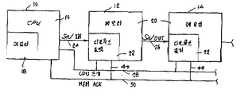
제1도는 프로세서(10)와 메모리 보드(12 및 14)를 포함하는 마이크로컴퓨터 시스템을 나타낸다. 본 발명이 두 개의 확장메모리 보드에 관하여 설명되더라도, 본 발명에 따른 컴퓨터 시스템이 이후에 설명될 제어신호에서 적당하게 증가하는 비트수에 의해 임의크기의 확장메모리 보드 수를 포함한다는 것을 이해하게 될 것이다.1 shows a microcomputer system including a
프로세서(10)는 내부 메모리(18)를 가진 중앙처리장치(CPU)(16)를 포함한다. CPU메모리(18)는 프로세서(10)의 많은 처리 작업에 충분한 용량이다. 그러나, 어떤 처리작업은 확장메모리 보드(12 및 14)에 의해 여유가 있는 부가메모리를 요구할 수도 있다. 각각의 메모리 보드(12 및 14)는 메모리(20)와 디코우드논리(22)를 포함한다.The
설명된 실시예에서, 메모리(20)는 본 기술분야에서 잘알려진 다이나믹 랜덤 억세스 메모리(DRAM)열을 포함한다. 그러한 열을 전체 또는 절반의 칩으로 구성될 수 있으며 1메가비트 또는 4메가비트 칩을 사용할 수도 있다. 메모리(20)는 전체를 1메가비트 칩으로 구성할 때 16메가바이트의 기억용량을 형성한다. 그러면, 그 메모리(20)는 1메가비트 절반으로 구성될때는 8메가바이트의 기억용량을 갖게 될것이며, 4메가비트의 칩이 사용될때에는 32 또는 64메가바이트의 기억용량을 갖게 된다는 것이 명백하다.In the described embodiment, the
CPU 메모리(18)는 구성면에서 반으로 구성된 메모리(20)와 유사하다. 그러므로, 1 또는 4메가비트 칩이사용됨에 따라 8 또는 32메가바이트의 기억용량을 갖는다.
CPU(16)는 CPU 메모리(18)를 개시하고 메모리 보드(12 및14)가 존재할 때 그들의 메모리 공간을 통해 연속하는 단일의 인접 메모리 공간을 가진것처럼 동작한다. 최하위 어드레스는 CPU 메모리(18)내의 메모리 장소와 대응한다. CPU 메모리(18) 용량보다 큰 어드레스는 메모리보드(12)상의 메모리(20)내의 메모리 장소에 대응한다. CPU 메모리(18)와 메모리보드(12)가 결합된 용량보다 더큰 어드레스는 메모리 보드(14)상에 메모리(20)의 메모리 장소에 대응한다. 이후에 설명되는 것처럼, CPU(16)는 어드레스 사용범위를 제한하기 위하여 전반적인 컴퓨터시스템에 유용한 메모리 공간의 전체양을 결정한다.The
각 메모리 보드(12 및 14)상의 디코우드 로직(22)은 메모리 (20)에 메모리양과 하위어드레스를 갖는 메모리양을 지정하는 즉, 메모리 보드(12)인 경우에는 CPU 메모리 (18)내의 메모리양을 지정하고 메모리 보드(14)인 경우에는 CPU 메모리(18)와 메모리 보드(12)의 결합된 메모리양을 지정하는 입력에 기초하여 대응 메모리(20)에 어드레싱 범위를 결정한다.The
메모리 보드(12)는 선(24)으로 CPU(16)으로부터 입력신호(SA/IN)를 수신한다. 비록 제1도에서는 단 하나의 선(24)으로 표시되어 있지만, 사실상 다수의 디지털 비트를 포함하는 디지털 정보를 상호연결할 때는 본 분야에 통상적인 다수의 병렬신호선으로 구성되어 있다는 것을 이해하게 된다. 설명된 실시예에서, 신호(SA/IN)는 3개의 디지털 비트로 구성된다. 그러므로, 선(24)은 3개의 병렬 전기도체로 구성된다. 유사하게, 이 명세를 통해 신호 “선”으로 부재된 곳은 어디에나 다수의 병렬 전기도체로 구성되고 그 수는 선상에 전송되는 비트수에 의해 결정된다는 것을 이해하게 될 것이다.The
신호(SA/IN)는 메모리 보드(12)에 최하위 어드레스를 갖는 메모리양을 표시하는 신호를 공급한다. 제1도의 설명처럼, 메모리 보드(12)는 프로세서(10)에 인접되어 있다. 그러므로, 오직 그러한 메모리는 CPU 메모리(18)뿐이다.The signal SA / IN supplies the
상기 설명처럼, CPU 메모리(18)는 8메가바이트나 32메가바이트의 용량을 가질 수 있다. 그러나 CPU 메모리(18)의 크기를 무시하고 CPU(16)는 SA/IN의 모든 비트가 논리적인 출력을 선(24)에 공급한다. SA/IN의 이러한 상태는 보드메모리 어드레스가 CPU 메모리(18)의 어드레스를 따른다는 것을 메모리 보드(12)의 디코우드 로직(22)에 표시한다.As described above, the
또한 CPU(16)는 선(28)에 출력(CPU 크기)를 공급한다. 이 출력은 확장메모리 보드에 CPU 메모리(18)내의 메모리양을 표시하는데 사용된다. 상기 설명처럼, 언급된 실시예의 CPU 메모리(18)는 8 또는 32 메가바이트 일 수 있다. 그래서, 신호(CPU 크기)는 오직 코어(core) 메모리(18)의 두 개의 가능한 구성을 나타내는 일 비트를 포함해야할 필요가 있다. 잘알려진 로직회로설계기술을 사용하여, 메모리 보드(12)의 디코우드 로직(22)은 입력신호(SA/IN 및 CPU 크기)로 구성된 정보를 결합하여 메모리 보드(12)의 메모리(20)에 제1메모리 위치의 어드레스를 결정한다.The
제4도에 도시된것처럼, 디코우드 로직(22)은 또한 메모리(20)의 용량을 나타내는 입력(MEM 크기)을 수신한다. 상기 설명처럼, 메모리(20)는 8,16,32 또는 64메가비트중 아무것이나 포함할 수 있다. 그래서 신호(MEM 크기)는 메모리(20)의 4개의 가능한 구성을 나타내는 오직 2비트를 포함하지 않으면 안된다. 물론 메모리(20)의 크기는 메모리 보드를 제조할 때 공지된다. 메모리 보드를 제조하는 동안 디코우드 로직(22)에 입력되는 MEM 크기용으로 적당한 2비트 코드를 공급하기 위하여 점퍼들이 장착된다. 이전설명처럼 메모리(20)에서 제1메모리 장소의 어드레스를 알고 그 메모리 보드상의 메모리양을 알기 때문에, 메모리 보드,(12)의 디코우드 로직(22)은 인접한 확장 메모리 보드(26)용으로 적당한 개시어드레스 코드를 결정한다. 이코드는 선(26)에 신호(SA/OUT)로 제공된다.As shown in FIG. 4, the
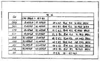
설명의 목적을 위해, 제2도는 확장메모리 보드를 2개까지 수용할 수 있는 실시예에서 제1메모리 보드(즉, 보드 12)의 신호(SA/OUT)와 결합가능한 각각의 디지털 워드를 표로 표시한다. 이전에 설명된것처럼, 실시예의 CPU 메모리(18)는 2개의 상이한 크기중 하나를 가질 수 있다. CPU 메모리(18)의 크기를 X라 하자. 역시 설명된것처럼, 메모리 보드(12)의 메모리(20)는 4개의 상이한 크기중 어느 하나를 가질 수 있다.For illustration purposes, FIG. 2 tabulates each digital word that can be combined with the signal SA / OUT of the first memory board (ie, board 12) in an embodiment that can accommodate up to two expansion memory boards. do. As previously described, the
메모리 보드(12)중의 메모리(20)의 크기를 Y1이라 하자. 그러면, 메모리 보드(14)의 앞에(즉, 보다 하위어드레스를 가진) 8개의 가능한 메모리 크기(X+Y1)로 결합할 수 있다. 예를 들어, 메모리 보드(12)의 디코우드 로직(22)이 CPU 메모리(18)가 8메가바이트를 나타내는 CPU 크기 입력을 수신하고, 보드(12)의 메모리(20)가 8메가바이트를 나타내는 MEM 크기 입력을 수신한다면, 보드(12)의 신호(SA/OUT)중 3비트 모두는 로직제로로 세트된다. 메모리 보드(14)의 디코우드 로직(22)은 그 이전에 16메가비트의 총메모리용량(X+Y1)이 있다는 것을 알려준다.Assume that the size of the
확장 메모리 보드(14)의 디코우드 로직(22)은 메모리 보드(12)의 디코우드 로직(22)으로부터 신호(SA/OUT)를 선(26)상에서 입력(SA/IN)으로서 수신한다. 메모리 보드(12)와 연결되어 상기 설명된 것과 유사한 방법으로, 메모리 보드(14)이 디코우드 로직(22)은 메모리 보드(14)에 장착된 메모리(20)의 크기를 지시하는 신호(MEM 크기)에 입력(SA/IN)을 결합시킨다. 이 후자값을 Y2라고 표시하자. 메모리 보드(14)의 디코우드 로직(22)은 어드레스 영역(Y2)에 대응하는 어드레스의 범위를 유도한다. 메모리 보드(14)의 디코우드 로직(22)은 또한 CPU메모리(18)와 메모리 보드(12 및 14)에 유용한 총 메모리양을 나타내는 X-Y1+Y2를 유도한다. 두 개이상의 확장메모리 슬롯을 포함하는 실시예에서, 이값의 디지털 코드 표시는 인접한 확장메모리 보드(도시되지 않음)에 제공된다.
메모리 보드(12)가 시스템에 장착되지 않는다면, 선(26)은 개방회로가 되었다는 것을 알 수 있다. 이러한 우발성을 제공하기 위하여, 디코우드 로직(22)은 SA/IN 입력의 모든 비트에 풀업(pull up) 저항을 구비한다. 풀업저항(40)은 제1도의 선(26)처럼 입력을 공급하는 선이 개방회로라면 입력(SA/IN)의 모든 비트가 로직 1로 나타나게 된다는 것을 보증한다.If the
이경우에, 제2도에서 처럼, 메모리 보드(14)의 디코우드 로직(22)은 그 이전의 메모리가 단지 CPU 메모리라는 것을 알려줄 것이다. 이런 방식으로, 메모리 보드는 인접 프로세서(10)를 물리적으로 슬롯에 구속시키는것보다는 이용가능한 어느 슬롯에나 삽입될 수가 있다. 그러나 2이상의 이용가능한 슬롯을 가진 시스템에서, 일 이상의 확장 메모리보드가 사용된다면 그 보드들은 인접 슬롯에 장착되어야만 한다. 만약 그렇지 않고, 보드간에 빈 슬롯이 있다면 이전의 빈슬롯을 가진 보드는 제1메모리 보드가 되도록 나타날 것이다.In this case, as in FIG. 2, the
이전에 설명된 것처럼, 각각의 확장메모리 보드의 디코우드 로직(22)은 그 보드상에서 피지칼 메모리 스페이스 레지던트(physical memory space resident)에 대응하는 어드레스의 범위를 결정할 수 있다. 제4도에 도시된것처럼, 디코우드 로직(22)은 CPU(16)가 메모리 장소에 억세스될 때마다 최상위 어드레스 비트를 선(42)상에서 입력으로 수신한다.As previously described, the
설명한 실시예에서 확장메모리의 최소증가가 8메가바이트(223바이트)이기 때문에, 23최하위 어드레스 비트는 확장 메모리의 증가가 어드레스 되는 것을 결정하는데 무관하다는 것을 알게될 것이다. 그래서, 오직 최상위 어드레스 비트는 입력으로서 디코우드 로직(22)에 필요하다. 그런, 23최하위 어드레스비트중 어느것은 이후에 설명될 메모리 서브어레이(sub-array)를 규정하기 위하여 디코우드 로직(22)에 제공될 수 있다.Since the minimum increase of the expansion memory in the described embodiment is 8 megabytes (223 bytes), it will be appreciated that the 23 least significant address bits are irrelevant in determining that an increase in expansion memory is addressed. Thus, only the most significant address bits are needed by the
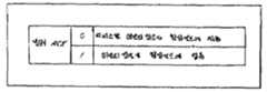
입력(42)상의 어드레스 비트가 메모리(20)의 어드레스범위내의 어드레스에 대응할때는 언제나 디코우드로직(22)은 선(24)상이 출력(MEM ACK)을 논리제로로 세트하고, 그렇지 않으면 MEM ACK는 논리 1로 세트된다. 설명된 신호(MEM ACK)의 극성은 단지 편리를 위한 것이며, 역극성도 본 분야에 숙달된 사람에 의해 선택적으로 설계될 수 있다.Whenever the address bit on the
각각의 확장메모리 보드의 MEM ACK 출력은 입력선(30)을 통해 CPU(16)에 연결된다. 본 기술분야에서 잘알려져 있는것처럼, 출력신호(MEM ACK)에 대한 디코우드 로직(22)내의 출력회로(도시되지 않음)는 어느하나의 출력선(44)이 논리제로로 세트되어 선(30)도 역시 논리제로를 표시한다면, 반면에 모든 출력선(40)이 논리 1로 세트될때만 선(30)은 논리 1을 표시하도록 구성된다. 그래서, CPU(16)가 확장메모리 보드중 어느 하나의 피지칼 어드레스 스페이스에 있는 메모리 장소를 억세스 할 때마다. 선(30)은 논리 제로로 수신될 것이다.The MEM ACK output of each expansion memory board is connected to the
이용가능한 총 메모리 공간과 이용가능한 어드레스의 최대 영역을 결정하기 위하여, CPU(16)는 초기루틴을 실행한다. 그러한 루틴에서, CPU(16)는 확장 메모리의 증가에 대응하는 메모리 경계, 즉 상기 실시예에서 8메가바이트를 어드레스하게 한다. 각각의 경계어드레스가 발생됨에 따라, 신호(MEM ACK)가 테스트된다. MEM ACK가 논리 제로라면, 다음 경계어드레스가 발생된다. MEM ACK이 논리 1로 결정될 때, CPU(16)는 발생된 어드레스가 이용가능한 메모리 공간을 초과한다는 것을 인식하여 즉시 최대 어드레스 영역값을 기억한다. 보통의 기술을 가진 컴퓨터 프로그램의 능력으로도 방금 설명된 단계를 실행하는 컴퓨터 프로그램을 작성할 수 있다.In order to determine the total memory space available and the maximum area of available addresses, the
상기 설명처럼, CPU(16)는 확장 메모리 보드(12 및 14)중 하나 또는 두 개 모두 장착되거가 또는 두 개모두 장착되지 않는지를 이용가능한 메모리 양으로 결정할 수 있다. 게다가, CPU(16)는 CPU 메모리(18)와 메모리(20)의 어떠한 조합적 구성에 대하여도 이용가능한 메모리양을 결정할 수 있다.As described above, the
메모리(20)에서 데이터의 저장 및 검색은 필수적인 종래의 방식으로 이루어진다. 제4도에 도시되었던것처럼, 메모리(20)는 데이터버스(56)상에서 프로세서(10)으로부터 데이터를 수신하고 프로세서(10)로 데이터를 공급한다. 메모리 어드레스는 선(48)에서 프로세서(10)로부터 어드레스 버퍼(46)에 의해 수신된다. 그후 어드레스는 차례로 어드레스를 메모리(20)로 공급하는 라인 구동기(50)에 공급된다. 프로세서(10)는 선(52 및 54)에서 각각 로우 어드레스 스트로우브(RAS)와 컬럼 어드레스 스트로우브(CAS) 신호를 공급한다. 제어 메모리 억세스로의 그러한 신호의 사용은 본분야에서 잘 알려져 있다. RAS 신호가 메모리(20)에 직접 공급되지만 CAS 신호는 디코우드 로직(22)에 공급된다. 여기에 설명된 실시예에서, 메모리(20)는 4개의 서브어레이 메모리로 분할된다. 상기 설명처럼, 디코우드 로직(22)은 일정한 최상위 어드레스 비트를 프로세스하여 출력(MEM ACK)을 발생한다. 디코우드 로직(22)이 어드레스가 메모리(10)에서 피지칼 메모리 스페이스 레지던트와 대응한다는 것을 결정한다면, 그것은 선(54)에서 CAS 신호의 수신에 동기하여 메모리(20)로 신호(CAS1, CAS2, CAS3, 또는 CAS4)중 하나를 공급한다. 디코우드 로직(22)은 4개의 서브 어레이가 어드레스되는 것에 기초하여 적당한 CAS신호를 발생한다.The storage and retrieval of data in the
상기 설명된 발명이 사상과 필수적인 특성을 벗어남이 없이 다른 특수한 형태로 실시될 수 있다는 것을 인식하게 될 것이다. 그러므로, 본 발명은 첨부된 청구범위에 설명된 것이외의 이미 설명된 명세에 의해 한정되지 않다는 것을 알 수 있다.It will be appreciated that the invention described above may be embodied in other specific forms without departing from the spirit and essential characteristics thereof. Therefore, it is to be understood that the invention is not limited by the already described specification other than as described in the appended claims.
Claims (9)
Translated fromKoreanApplications Claiming Priority (2)
| Application Number | Priority Date | Filing Date | Title |
|---|---|---|---|
| US07/164,092US4951248A (en) | 1988-03-04 | 1988-03-04 | Self configuring memory system |
| US164,092 | 1988-03-04 |
Publications (2)
| Publication Number | Publication Date |
|---|---|
| KR890015136A KR890015136A (en) | 1989-10-28 |
| KR920010974B1true KR920010974B1 (en) | 1992-12-26 |
Family
ID=22592943
Family Applications (1)
| Application Number | Title | Priority Date | Filing Date |
|---|---|---|---|
| KR1019880015413AExpiredKR920010974B1 (en) | 1988-03-04 | 1988-11-23 | Self configuring memory system |
Country Status (9)
| Country | Link |
|---|---|
| US (1) | US4951248A (en) |
| JP (1) | JP2717693B2 (en) |
| KR (1) | KR920010974B1 (en) |
| AU (1) | AU622119B2 (en) |
| CA (1) | CA1323114C (en) |
| DE (1) | DE3906497A1 (en) |
| FR (1) | FR2628234B1 (en) |
| GB (1) | GB2215497B (en) |
| HK (1) | HK95393A (en) |
Families Citing this family (49)
| Publication number | Priority date | Publication date | Assignee | Title |
|---|---|---|---|---|
| US5148389A (en)* | 1988-04-05 | 1992-09-15 | Convergent Technologies, Inc. | Modular expansion bus configuration |
| US5257387A (en)* | 1988-09-09 | 1993-10-26 | Compaq Computer Corporation | Computer implemented method and apparatus for dynamic and automatic configuration of a computer system and circuit boards including computer resource allocation conflict resolution |
| GB2226667B (en)* | 1988-12-30 | 1993-03-24 | Intel Corp | Self-identification of memory |
| GB2226666B (en)* | 1988-12-30 | 1993-07-07 | Intel Corp | Request/response protocol |
| JPH02287646A (en)* | 1989-04-27 | 1990-11-27 | Toshiba Corp | Memory expansion method |
| KR910008413B1 (en)* | 1989-07-21 | 1991-10-15 | 삼성전자 주식회사 | Memory Capacity Expansion Unit |
| US5237672A (en)* | 1989-07-28 | 1993-08-17 | Texas Instruments Incorporated | Dynamically adaptable memory controller for various size memories |
| JP3024767B2 (en)* | 1989-08-29 | 2000-03-21 | 株式会社日立製作所 | Address supply system |
| EP0419869A3 (en)* | 1989-09-29 | 1992-06-03 | Kabushiki Kaisha Toshiba | Personal computer for accessing two types of extended memories having different memory capacities |
| EP0428021B1 (en)* | 1989-11-03 | 1998-09-02 | Compaq Computer Corporation | Method for data distribution in a disk array |
| US5271098A (en)* | 1989-11-07 | 1993-12-14 | Chips And Technologies, Inc. | Method and apparatus for use of expanded memory system (EMS) to access cartridge memory |
| US5012408A (en)* | 1990-03-15 | 1991-04-30 | Digital Equipment Corporation | Memory array addressing system for computer systems with multiple memory arrays |
| US5325497A (en)* | 1990-03-29 | 1994-06-28 | Micro Technology, Inc. | Method and apparatus for assigning signatures to identify members of a set of mass of storage devices |
| JPH03282648A (en)* | 1990-03-29 | 1991-12-12 | Sharp Corp | memory controller |
| JP2997005B2 (en)* | 1990-04-12 | 2000-01-11 | キヤノン株式会社 | Output device |
| US5175833A (en)* | 1990-06-07 | 1992-12-29 | Intel Corporation | Apparatus for determining relative position of a cache memory in a cache memory array |
| JPH05108484A (en)* | 1990-06-07 | 1993-04-30 | Intel Corp | Cache memory |
| US5249277A (en)* | 1990-08-08 | 1993-09-28 | Compuadd Corporation | Optimized performance memory method and system |
| DE69131958T2 (en)* | 1990-09-17 | 2000-10-12 | Samsung Semiconductor, Inc. | Procedure for configuring a storage system |
| EP0551387A1 (en)* | 1990-09-25 | 1993-07-21 | Digital Equipment Corporation | Apparatus and methods for distributed address decoding and memory configuration |
| US5522064A (en)* | 1990-10-01 | 1996-05-28 | International Business Machines Corporation | Data processing apparatus for dynamically setting timings in a dynamic memory system |
| US5530934A (en)* | 1991-02-02 | 1996-06-25 | Vlsi Technology, Inc. | Dynamic memory address line decoding |
| US5448710A (en)* | 1991-02-26 | 1995-09-05 | Hewlett-Packard Company | Dynamically configurable interface cards with variable memory size |
| US5761479A (en)* | 1991-04-22 | 1998-06-02 | Acer Incorporated | Upgradeable/downgradeable central processing unit chip computer systems |
| US5551012A (en)* | 1991-04-22 | 1996-08-27 | Acer Incorporated | Single socket upgradeable computer motherboard with automatic detection and socket reconfiguration for inserted CPU chip |
| EP0510241A3 (en)* | 1991-04-22 | 1993-01-13 | Acer Incorporated | Upgradeable/downgradeable computer |
| JPH04336347A (en)* | 1991-05-13 | 1992-11-24 | Ricoh Co Ltd | memory device |
| JPH0715665B2 (en)* | 1991-06-10 | 1995-02-22 | インターナショナル・ビジネス・マシーンズ・コーポレイション | Personal computer |
| EP0525308A1 (en)* | 1991-07-31 | 1993-02-03 | International Business Machines Corporation | Memory map for processor cache macro |
| EP0529142A1 (en)* | 1991-08-30 | 1993-03-03 | Acer Incorporated | Upgradeable/downgradeable computers |
| JPH05225046A (en)* | 1991-11-12 | 1993-09-03 | Internatl Business Mach Corp <Ibm> | Memory subsystem which can be constituted |
| US5317712A (en)* | 1991-12-19 | 1994-05-31 | Intel Corporation | Method and apparatus for testing and configuring the width of portions of a memory |
| JPH05210576A (en)* | 1992-01-21 | 1993-08-20 | Nec Corp | Storage device and setting method for its address |
| US5428762A (en)* | 1992-03-11 | 1995-06-27 | International Business Machines Corporation | Expandable memory having plural memory cards for distributively storing system data |
| JP2724078B2 (en)* | 1992-09-29 | 1998-03-09 | 株式会社日立製作所 | Maintenance method for redundant memory |
| US5598540A (en)* | 1992-09-30 | 1997-01-28 | Texas Instruments Incorporated | Memory module including read-write memory and read-only configuration memory accessed only sequentially and computer system using at least one such module |
| JPH06139182A (en)* | 1992-10-27 | 1994-05-20 | Sony Corp | Information processor, extended substrate, and extended enclosure system |
| US5509138A (en)* | 1993-03-22 | 1996-04-16 | Compaq Computer Corporation | Method for determining speeds of memory modules |
| US5594879A (en)* | 1993-10-29 | 1997-01-14 | Compaq Computer Corporation | Method of and apparatus for arbitrarily disabling under processor control individual slots on a computer bus |
| US5452429A (en)* | 1993-11-17 | 1995-09-19 | International Business Machines Corporation | Error correction code on add-on cards for writing portions of data words |
| US5488691A (en)* | 1993-11-17 | 1996-01-30 | International Business Machines Corporation | Memory card, computer system and method of operation for differentiating the use of read-modify-write cycles in operating and initializaiton modes |
| JPH08115592A (en)* | 1994-10-14 | 1996-05-07 | Sega Enterp Ltd | Data processing system, data processing method, and memory cassette |
| US5941775A (en)* | 1994-10-14 | 1999-08-24 | Sega Of America, Inc. | Data processing system, method thereof and memory cassette |
| US5809555A (en)* | 1995-12-15 | 1998-09-15 | Compaq Computer Corporation | Method of determining sizes of 1:1 and 2:1 memory interleaving in a computer system, configuring to the maximum size, and informing the user if memory is incorrectly installed |
| US6505268B1 (en) | 1996-12-20 | 2003-01-07 | Compaq Computer Corporation | Data distribution in a disk array |
| US6067593A (en)* | 1997-07-18 | 2000-05-23 | Avido Systems, Inc. | Universal memory bus and card |
| US6114946A (en)* | 1998-09-10 | 2000-09-05 | Lsi Logic Corporation | Combinational logic for comparing N-bit wide buses |
| US7308527B2 (en)* | 2005-01-24 | 2007-12-11 | International Business Machines Corporation | System for indicating a plug position for a memory module in a memory system |
| EP2511825A4 (en)* | 2011-05-28 | 2013-01-23 | Huawei Device Co Ltd | Method and device for configuring memory capacity |
Family Cites Families (10)
| Publication number | Priority date | Publication date | Assignee | Title |
|---|---|---|---|---|
| US3864151A (en)* | 1973-07-02 | 1975-02-04 | Anchor Hocking Corp | Glass article coated with plastic and lubricity coatings and method of coating |
| US4025903A (en)* | 1973-09-10 | 1977-05-24 | Computer Automation, Inc. | Automatic modular memory address allocation system |
| US3872452A (en)* | 1974-04-17 | 1975-03-18 | Ibm | Floating addressing system and method |
| JPS55110355A (en)* | 1979-02-16 | 1980-08-25 | Toshiba Corp | Memory board and selection system for it |
| US4303993A (en)* | 1979-10-10 | 1981-12-01 | Honeywell Information Systems Inc. | Memory present apparatus |
| US4609996A (en)* | 1983-08-12 | 1986-09-02 | International Business Machines Corporation | Memory access system for a computer system adapted to accept a memory expansion module |
| US4727475A (en)* | 1984-05-18 | 1988-02-23 | Frederick Kiremidjian | Self-configuring modular computer system with automatic address initialization |
| US4744025A (en)* | 1985-05-02 | 1988-05-10 | Digital Equipment Corporation | Arrangement for expanding memory capacity |
| AU579725B2 (en)* | 1985-05-02 | 1988-12-08 | Digital Equipment Corporation | Arrangement for expanding memory capacity |
| US4740916A (en)* | 1985-12-19 | 1988-04-26 | International Business Machines Corporation | Reconfigurable contiguous address space memory system including serially connected variable capacity memory modules and a split address bus |
- 1988
- 1988-03-04USUS07/164,092patent/US4951248A/ennot_activeExpired - Lifetime
- 1988-09-27GBGB8822602Apatent/GB2215497B/ennot_activeExpired - Fee Related
- 1988-11-21AUAU25744/88Apatent/AU622119B2/ennot_activeCeased
- 1988-11-23KRKR1019880015413Apatent/KR920010974B1/ennot_activeExpired
- 1988-12-20FRFR8816823Apatent/FR2628234B1/ennot_activeExpired - Fee Related
- 1989
- 1989-01-05CACA000587584Apatent/CA1323114C/ennot_activeExpired - Fee Related
- 1989-03-01DEDE3906497Apatent/DE3906497A1/ennot_activeWithdrawn
- 1989-03-03JPJP1051840Apatent/JP2717693B2/ennot_activeExpired - Fee Related
- 1993
- 1993-09-16HKHK953/93Apatent/HK95393A/ennot_activeIP Right Cessation
Also Published As
| Publication number | Publication date |
|---|---|
| US4951248A (en) | 1990-08-21 |
| GB2215497A (en) | 1989-09-20 |
| GB2215497B (en) | 1992-07-08 |
| HK95393A (en) | 1993-09-24 |
| KR890015136A (en) | 1989-10-28 |
| CA1323114C (en) | 1993-10-12 |
| AU622119B2 (en) | 1992-04-02 |
| AU2574488A (en) | 1989-09-07 |
| FR2628234A1 (en) | 1989-09-08 |
| GB8822602D0 (en) | 1988-11-02 |
| JPH01267752A (en) | 1989-10-25 |
| FR2628234B1 (en) | 1993-09-24 |
| JP2717693B2 (en) | 1998-02-18 |
| DE3906497A1 (en) | 1989-09-14 |
Similar Documents
| Publication | Publication Date | Title |
|---|---|---|
| KR920010974B1 (en) | Self configuring memory system | |
| US4926314A (en) | Method and apparatus for determining available memory size | |
| US6092146A (en) | Dynamically configurable memory adapter using electronic presence detects | |
| KR910000589B1 (en) | Memory system providing contiguous address space | |
| US5966727A (en) | Combination flash memory and dram memory board interleave-bypass memory access method, and memory access device incorporating both the same | |
| EP0549139B1 (en) | Programmable memory timing | |
| US7133960B1 (en) | Logical to physical address mapping of chip selects | |
| US5283877A (en) | Single in-line DRAM memory module including a memory controller and cross bar switches | |
| US5907512A (en) | Mask write enablement for memory devices which permits selective masked enablement of plural segments | |
| USRE36229E (en) | Simulcast standard multichip memory addressing system | |
| US4545010A (en) | Memory identification apparatus and method | |
| US6414868B1 (en) | Memory expansion module including multiple memory banks and a bank control circuit | |
| US4908789A (en) | Method and system for automatically assigning memory modules of different predetermined capacities to contiguous segments of a linear address range | |
| US5278801A (en) | Flexible addressing for drams | |
| US5535368A (en) | Automatically-configuring memory subsystem | |
| US5446860A (en) | Apparatus for determining a computer memory configuration of memory modules using presence detect bits shifted serially into a configuration register | |
| KR970705810A (en) | IMPROVED MEMORY ARCHITECTURE AND DEVICES, SYSTEMS AND METHODS UTILIZING THE SAME, AND METHOD AND APPARATUS THEREFOR | |
| US5572692A (en) | Memory configuration decoding system having automatic row base address generation mechanism for variable memory devices with row access interleaving | |
| US5179686A (en) | Method for automatically detecting the size of a memory by performing a memory warp operation | |
| US6470417B1 (en) | Emulation of next generation DRAM technology | |
| US4882700A (en) | Switched memory module | |
| US4796222A (en) | Memory structure for nonsequential storage of block bytes in multi-bit chips | |
| JPS62237542A (en) | Memory | |
| EP0200198B1 (en) | An arrangement for expanding memory capacity | |
| US4992979A (en) | Memory structure for nonsequential storage of block bytes in multi bit chips |
Legal Events
| Date | Code | Title | Description |
|---|---|---|---|
| PA0109 | Patent application | St.27 status event code:A-0-1-A10-A12-nap-PA0109 | |
| R17-X000 | Change to representative recorded | St.27 status event code:A-3-3-R10-R17-oth-X000 | |
| P11-X000 | Amendment of application requested | St.27 status event code:A-2-2-P10-P11-nap-X000 | |
| P13-X000 | Application amended | St.27 status event code:A-2-2-P10-P13-nap-X000 | |
| PG1501 | Laying open of application | St.27 status event code:A-1-1-Q10-Q12-nap-PG1501 | |
| A201 | Request for examination | ||
| PA0201 | Request for examination | St.27 status event code:A-1-2-D10-D11-exm-PA0201 | |
| P11-X000 | Amendment of application requested | St.27 status event code:A-2-2-P10-P11-nap-X000 | |
| P13-X000 | Application amended | St.27 status event code:A-2-2-P10-P13-nap-X000 | |
| E902 | Notification of reason for refusal | ||
| PE0902 | Notice of grounds for rejection | St.27 status event code:A-1-2-D10-D21-exm-PE0902 | |
| P11-X000 | Amendment of application requested | St.27 status event code:A-2-2-P10-P11-nap-X000 | |
| P13-X000 | Application amended | St.27 status event code:A-2-2-P10-P13-nap-X000 | |
| G160 | Decision to publish patent application | ||
| PG1605 | Publication of application before grant of patent | St.27 status event code:A-2-2-Q10-Q13-nap-PG1605 | |
| E701 | Decision to grant or registration of patent right | ||
| PE0701 | Decision of registration | St.27 status event code:A-1-2-D10-D22-exm-PE0701 | |
| GRNT | Written decision to grant | ||
| PR0701 | Registration of establishment | St.27 status event code:A-2-4-F10-F11-exm-PR0701 | |
| PR1002 | Payment of registration fee | St.27 status event code:A-2-2-U10-U11-oth-PR1002 Fee payment year number:1 | |
| PR1001 | Payment of annual fee | St.27 status event code:A-4-4-U10-U11-oth-PR1001 Fee payment year number:4 | |
| PR1001 | Payment of annual fee | St.27 status event code:A-4-4-U10-U11-oth-PR1001 Fee payment year number:5 | |
| PR1001 | Payment of annual fee | St.27 status event code:A-4-4-U10-U11-oth-PR1001 Fee payment year number:6 | |
| PR1001 | Payment of annual fee | St.27 status event code:A-4-4-U10-U11-oth-PR1001 Fee payment year number:7 | |
| R18-X000 | Changes to party contact information recorded | St.27 status event code:A-5-5-R10-R18-oth-X000 | |
| PN2301 | Change of applicant | St.27 status event code:A-5-5-R10-R13-asn-PN2301 St.27 status event code:A-5-5-R10-R11-asn-PN2301 | |
| PR1001 | Payment of annual fee | St.27 status event code:A-4-4-U10-U11-oth-PR1001 Fee payment year number:8 | |
| PR1001 | Payment of annual fee | St.27 status event code:A-4-4-U10-U11-oth-PR1001 Fee payment year number:9 | |
| PR1001 | Payment of annual fee | St.27 status event code:A-4-4-U10-U11-oth-PR1001 Fee payment year number:10 | |
| FPAY | Annual fee payment | Payment date:20030124 Year of fee payment:11 | |
| PR1001 | Payment of annual fee | St.27 status event code:A-4-4-U10-U11-oth-PR1001 Fee payment year number:11 | |
| R18-X000 | Changes to party contact information recorded | St.27 status event code:A-5-5-R10-R18-oth-X000 | |
| LAPS | Lapse due to unpaid annual fee | ||
| PC1903 | Unpaid annual fee | St.27 status event code:A-4-4-U10-U13-oth-PC1903 Not in force date:20031227 Payment event data comment text:Termination Category : DEFAULT_OF_REGISTRATION_FEE | |
| PC1903 | Unpaid annual fee | St.27 status event code:N-4-6-H10-H13-oth-PC1903 Ip right cessation event data comment text:Termination Category : DEFAULT_OF_REGISTRATION_FEE Not in force date:20031227 | |
| P22-X000 | Classification modified | St.27 status event code:A-4-4-P10-P22-nap-X000 |