KR920009192B1 - Sub-unit for snoop interface - Google Patents
Sub-unit for snoop interfaceDownload PDFInfo
- Publication number
- KR920009192B1 KR920009192B1KR1019890019507AKR890019507AKR920009192B1KR 920009192 B1KR920009192 B1KR 920009192B1KR 1019890019507 AKR1019890019507 AKR 1019890019507AKR 890019507 AKR890019507 AKR 890019507AKR 920009192 B1KR920009192 B1KR 920009192B1
- Authority
- KR
- South Korea
- Prior art keywords
- control signal
- signal line
- snoop
- local
- asserted
- Prior art date
- Legal status (The legal status is an assumption and is not a legal conclusion. Google has not performed a legal analysis and makes no representation as to the accuracy of the status listed.)
- Expired
Links
Images


Classifications
- G—PHYSICS
- G06—COMPUTING OR CALCULATING; COUNTING
- G06F—ELECTRIC DIGITAL DATA PROCESSING
- G06F12/00—Accessing, addressing or allocating within memory systems or architectures
- G06F12/02—Addressing or allocation; Relocation
- G06F12/08—Addressing or allocation; Relocation in hierarchically structured memory systems, e.g. virtual memory systems
- G06F12/0802—Addressing of a memory level in which the access to the desired data or data block requires associative addressing means, e.g. caches
- G06F12/0806—Multiuser, multiprocessor or multiprocessing cache systems
- G06F12/0815—Cache consistency protocols
- G06F12/0831—Cache consistency protocols using a bus scheme, e.g. with bus monitoring or watching means
Landscapes
- Engineering & Computer Science (AREA)
- Theoretical Computer Science (AREA)
- Physics & Mathematics (AREA)
- General Engineering & Computer Science (AREA)
- General Physics & Mathematics (AREA)
- Memory System Of A Hierarchy Structure (AREA)
Abstract
Translated fromKoreanDescription
Translated fromKorean제 1도는 본 발명의 회로도.1 is a circuit diagram of the present invention.
제 2도는 본 발명의 스눕 인터페이스 콘트롤러의 기능을 나타낸 블럭도.2 is a block diagram showing the functions of the snoop interface controller of the present invention.
제 3도는 본 발명의 스눕 인터페이스 콘트롤러가 글로벌 데이터의 엑세스를 시도하는 과정을 나타낸 플로우 챠트.3 is a flowchart illustrating a process in which the snoop interface controller of the present invention attempts to access global data.
제 4도는 본 발명의 스눕 인터페이스 콘트롤러가 글로벌 신호를 받은 상태의 과정을 나타낸 플로우 챠트.4 is a flowchart illustrating a process of a snoop interface controller according to the present invention receiving a global signal.
* 도면의 주요 부분에 대한 부호의 설명* Explanation of symbols for the main parts of the drawings
1, 10 : 보드 2, 3, 11, 12 : 캐쉬 메모리1, 10:
4, 5, 13, 14 : 어드레스 래치 6, 15 : 라인 선택부4, 5, 13, 14: address latch 6, 15: line selector
7, 16 : 스눕 인터페이스 서브 유니트 8 : 공유 메모리7, 16: snoop interface subunit 8: shared memory
본 발명은 다중 처리 시스템에서의 스눕 인터페이스(Snoop Interface)에 관한 것으로, 특히 캐쉬 코히어런스(Cache Coherence) 프로토콜을 로컬버스의 차원이 아닌 시스템 버스의 차원에서 이루어지도록 한 스눕 인터페이스 방법 및 그 장치에 관한 것이다.The present invention relates to a snoop interface in a multi-processing system, and more particularly, to a snoop interface method and apparatus for caching a cache coherence protocol in a system bus rather than a local bus. It is about.
다중 처리 시스템의 프로세서에 정의한 캐쉬 코히어런스에서는 로컬버스를 스누핑(snooping) 하는 기능이 포함되어 있었다. 그러나 하나의 보드(board)에 두 개의 프로세서 모듈이 서로 독립적으로 존재하고, 이에 따라 로컬 버스도 서로 분리되어 있는 상태이므로, 캐쉬 메모리의 내용과 주기억 장치(main memory)인 공유 메모리의 내용을 일치시키기 위하여(즉, 캐쉬 코히어런스를 위하여) 스누핑(Snooping) 한다는 것은 의미가 없다.Cache coherence, defined for processors in multiprocessing systems, included the ability to snoop on the local bus. However, since two processor modules exist on a board independently of each other, and the local buses are separated from each other, the contents of the cache memory and the shared memory that is the main memory are matched. It doesn't make sense to snoop for you (i.e. for cache coherence).
더우기, 다중 처리 시스템의 전체 구성으로 볼 때 각 프로세서 모듈이 속한 로컬버스는 전체 시스템이 공유하는 버스가 아니기 때문에 스누핑의 의미가 없게 된다.In addition, the overall configuration of a multi-processing system makes the local bus to which each processor module belong is not a bus shared by the entire system, which makes no sense of snooping.
이에 따라 본 발명은 캐쉬 코히어런스 프로토콜(cache coherence protocol)이 시스템 버스의 차원에서 이루어지도록 하는 스눕 인터페이스 방법 및 그 장치를 제공하는 것을 목적으로 한다.Accordingly, an object of the present invention is to provide a snoop interface method and apparatus for allowing a cache coherence protocol to be implemented in the dimension of a system bus.
본 발명은 첨부 도면에 의거 상세히 기술하여 보면 다음과 같다.The present invention will be described in detail with reference to the accompanying drawings.
제 1도는 본 발명의 개략적인 구성을 나타낸 것으로 동일한 보드 내에 존재하면서도 다른 로컬버스에 연결된 캐쉬 메모리에 대해서도, 다른 보드에 존재하는 캐쉬 메모리와 동일한 차원에서 스눕 인터페이스 서브 유니트를 통하여 캐쉬 코히어런시(cachy coherency)가 성립되는 과정을 나타낸 것이다.FIG. 1 is a schematic diagram of the present invention. For cache memory existing on the same board and connected to another local bus, cache coherency (Snop interface subunit) is provided through the snoop interface subunit in the same dimension as the cache memory existing on another board. cachy coherency) is shown.
두 개의 보드(1) (10)에 각각 두 개씩의 프로세서 모듈(도시되지 않음)이 존재하므로 각각 두 개씩의 캐쉬 메모리(2), (3)와 (11), (12)를 위치시키고, 각각의 캐쉬 메모리(2), (3), (11), (12)에서는 양 방향성의 어드레스래치(4), (5), (13), (14)를 거치고 라인 선택부(6), (15)를 경유하여 시스템 버스(100)와 연결하며, 시스템 버스(100)를 통하여 연결되는 공유메모리(8)는 물론, 보드(1), (10) 내의 캐쉬 메모리와 어드레스 래치 및 라인 선택부로 콘트롤 신호를 출력하는 두 스눕 인터페이스 콘트롤러(7), (16)에서는 상호간에도 콘트롤 신호를 주고 받는다.Since two processor modules (not shown) exist on each of the two boards (1) and (10), two cache memories (2), (3), (11), and (12), respectively, are placed. In the cache memory (2), (3), (11), (12) through the address latches (4), (5), (13), (14) of the bidirectional line selection section (6), (15) The control signal is connected to the
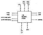
제 2도는 스눕 인터페이스 콘트롤러(7, 16)의 기능을 나타낸 것으로, 스눕 인터페이스 콘트롤러는 로컬버스 매스터(local bus master) 중 어느 하나(예를 들면, 캐쉬 메모리)가 글로벌 정보(global data)를 로우드(Load) 또는 기억(store)하기 위하여 주기억장치인 공유메모리(8)를 호출하면, 동시에 어서트(assert)하기 위한 콘트롤 신호(G1), (G2)와 로컬버스를 로크(Lock)하기 위한 콘트롤 신호(LK1), (LK2) 및 인텐트 투 모디 파이(Intent to modify)에 의한 읽기와 쓰기를 수행하기 위한 콘트롤 신호(IM1), (IM2)를 시스템 버스(100)가 동시에 로우딩(loading)해야 함으로써 파생되는 전송부하를 줄이기 위하여 스눕 인터페이스 콘트롤러(7, 16) 내의 양 방향성 버퍼(도시되지 않음)를 통하여 시스템 버스(100)의 G 신호선, LK 신호선 및 IM 신호선과 연결하고, 보드 내의 로컬버스 상태 신호선(LSTx)과 보드와 보드 사이의 시스템 버스 상태 신호선(SSTx)도 양 방향성 버퍼를 이용하여 연결한다.FIG. 2 shows the functions of the
여기서 ainq1, 2는 스누핑을 위하여 시스템 버스(100)의 신호선으로부터 들어온 어드레스 값을 로컬버스 콘트롤 서브 유니트 내에 있는 어드레서 래치(4, 5, 13, 14)에 입력시키기 위한 콘트롤 신호이며, aid11, 2는 어드래스 래치(4, 5, 13, 14)에 입력된 어드레스 값을 로컬버스로 출력시키기 위한 콘트롤 신호이며, select-snoop-path1, 2는 시스템 버스(100) 어드레스 신호선으로부터 주어진 어드레스 값을 보드(1, 10) 내로 입력시키는 경로를 라인 선택부(6, 15)를 통해 만들어 주기 위한 콘트롤 신호로서, 이 신호 1, 2는 시스템 버스(100)의 어드레스 신호선과 각 보드(1), (10) 내의 두 어드레스 래치(4, 4), (13, 14) 간의 경로를 형성하기 위해 라인 선택부(6, 15)의 두 어드레스 경로 중 프로세서 어느 하나 또는 둘 다 논리적으로 연결시키기 위한 신호이다.Here, ainq1 and 2 are control signals for inputting address values input from the signal line of the
그리고 snooping 신호는 현재 스누핑 동작이 수행 중에 있음을 로컬버스 사이클 콘트롤러(도시되지 않음)와 시스템 버스 사이클 콘트롤러(도시되지 않음)에게 알려주는 신호이다.The snooping signal is a signal informing the local bus cycle controller (not shown) and the system bus cycle controller (not shown) that a snooping operation is currently being performed.
그러므로 어느 하나의 로컬버스 매스터가 글로벌 정보를 로우드하거나 기억하기 위하여 공유메모리(8)를 억세스하게 되면 G 신호선 (또는/과 IM 신호선)이 어서트 된다.Therefore, when any local bus master accesses the shared
그 신호는 즉시 같은 보드(1) 내의 스눕 인터페이스 콘트롤러(7)로 전달되고, 그에 따라 스눕 인터페이스 콘트롤러(7)는 동일 보드(1)내의 다른 로컬 버스와의 어드레스 경로를 구성하기 위한 콘트롤 신호(select-snoop-path 2)를 라인 선택부(6)로 보낸다.The signal is immediately passed to the snoop interface controller 7 in the
그리고 어드레스의 역 방향 전달이 이루어지도록 어드레스래치(4), (5)를 구동하는 콘트롤 신호(ainq)(aidq)를 보낸다. 그와 동시에 다른 로컬 버스의 G 신호선과 시스템 버스의 G 신호선을 어서트시키고, 이 경우에는 캐쉬 코히어런스를 위해 사용되는 다른 콘트롤 신호(LK) (IM)에 대해서도 동일한 방법으로 시스템 전체의 각 로컬 버스로 전달된다.Then, a control signal (ainq) (aidq) for driving the address latches (4) and (5) is sent to reverse the transfer of the address. At the same time, it asserts the G signal line of the other local bus and the G signal line of the system bus, in which case each local throughout the system in the same way for the other control signal (LK) (IM) used for cache coherence. Delivered by bus.
한편, 다른 보드(10)에 있는 스눕 인터페이스 콘트롤러(16)는 시스템 버스 G 신호선이 어서트되면, 즉시 두 로컬버스에 속한 G 신호선을 어서트 시키는 동시에, 시스템 버스의 어드레스 신호선이 두 로컬버스의 어드레스 신호선으로 동시에 연결되는 경로를 만들어 주기 위한 콘트롤 신호(select-snoop-path 1과 2)를 라인 선택부(15)로 보낸다.On the other hand, when the system bus G signal line is asserted, the
그리고 어드레스 래치(13), (14) 들의 역 방향 전달이 이루어지도록 해당 콘트롤 신호(ainq) (aidq)를 보낸다. 그러면 다른 프로세서에서는 현재 진행중인 트랜잭션(transaction)을 중단하고 이를 우선적으로 처리한다.Then, a corresponding control signal (aidq) (aidq) is sent so that reverse transfer of the address latches (13) and (14) is performed. The other processor then aborts the current transaction and processes it first.
한편 콘트롤 신호(G)를 받은 각 캐쉬 메모리(2), (3) (11), (12)는 자신에 연결된 p-버스(private-bus)에서 수행되고 있는 상태를 알려주기 위한 신호(reply)의 신호선과 로컬버스의 상태 신호선(STx)을 통하여 "WAIT" 신호를 보낸다.On the other hand, each of the cache memories (2), (3) (11), and (12) receiving the control signal (G) is a signal for informing the status of being performed on the private bus connected to it. It sends 'WAIT' signal through the signal line of and the status signal line (STx) of the local bus.
만약, 이때 로컬 버스의 전달 과정에서 에러가 발생하였다면 로컬버스 상태 신호선(STx)의 에러 발생 신호선을 어서트하고, 원래 수행하던 동력으로 되돌아간다. 로컬버스의 전달과정에서 에러가 발생하지 않았다면 캐쉬 메모리의 태그(tag)를 검사하여 스누핑의 히트(hit) 또는 미스(miss)의 여부를 확인하고 미스인 경우에는 로컬버스의 상태 신호선(STx)의 사이클 종료 신호선(OK)을 어서트하지만, 히트인 경우에는 히트된 캐쉬엔트리(cache entry)의 상태에 따라 로컬버스의 상태 신호선(STx)의 재시도 신호선(Retry)를 어서트 하여 재시도를 요구하거나, 로컬버스의 상태 신호선(STx)의 사이클 종료 신호선(OK)을 어서트하고, 히트된 캐쉬엔트리의 상태 비트를 캐쉬 코히어런스 프로토콜에 맞게 변경한다.If an error occurs in the transfer process of the local bus at this time, the error occurrence signal line of the local bus status signal line STx is asserted, and the power is returned to the original power. If there is no error in the local bus transfer, check the tag of cache memory to check whether it is hit or miss of snooping. In case of miss, the status signal line (STx) of local bus The cycle end signal line OK is asserted, but in the case of a hit, the retry signal line Retry of the status signal line STx of the local bus is asserted according to the state of the hit cache entry, and a retry is requested. Alternatively, the cycle end signal line OK of the state signal line STx of the local bus is asserted, and the status bit of the hit cache entry is changed to match the cache coherence protocol.
이에 따라 각 캐쉬 메모리에서 어서트 된 로컬버스의 상태 신호선(STx)을 글로벌데이타 액세스를 시도했던 캐쉬 메모리까지 전달할 수 있는 직접 경로가 필요하게 되고, 이 로컬버스의 상태 신호선(STx)에 모든 캐쉬 메모리의 상태 신호선(STx)이 공동으로 연결되어야 하므로 로우딩의 문제가 발생할 수 있다.This requires a direct path from each cache memory to the asserted local bus status signal line (STx) to the cache memory that attempted to access the global data, and all cache memory on the local bus status signal line (STx). Since the state signal lines STx must be jointly connected, a problem of loading may occur.
그러므로 보드와 보드 사이의 연결은 버퍼를 통하여 연결하고, 이 버퍼를 스눕 인터페이스 콘트롤러 내에서 구현하게 되면 로컬 버스의 상태 신호선(STx)에서의 상호전달을 계층 구조를 갖게 된다.Therefore, the board-to-board connection is made through a buffer, and when this buffer is implemented in the snoop interface controller, it has a hierarchical structure of intercommunication on the status signal line (STx) of the local bus.
즉, 보드 내의 로컬버스의 상태 신호선(LSTx)은 스눕 인터페이스 콘트롤러에게로만 전달되고, 보드와 보드 사이의 상태 신호선(SSTx)은 각 보드의 스눕 인터페이스 콘트롤러들 사이에서 신호 전달이 이루어지도록 한다.That is, the status signal line LSTx of the local bus in the board is transmitted only to the snoop interface controller, and the status signal line SSTx between the board and the board allows signal transmission between snoop interface controllers of each board.
제 3도는 스눕 인터페이스 콘트롤러(7, 16)가 글로벌 데이터의 액세스를 시도하는 과정으로 나타낸 것으로, 글로벌 호출을 시도한 캐쉬 메모리와 같은 보드에 있는 스눕 인터페이스 콘트롤러의 기능을 나타낸 것이다.3 illustrates the process of
공유메모리(8)를 호출하면 어서트 되는 콘트롤 신호(G1)와, 로컬버스를 로크 하기 위한 콘트롤 신호(LK1)와, 인텐트 투 모디파이에 의한 읽기와 쓰기를 수행할 때 어서트 되는 콘트롤 신호(LM1) 중 하나가 입력되면 (단계 20), 같은 보드 내의 다른 프로세서 모듈로의 경로를 만들어 주기 위한 콘트롤 신호 즉, 라인 선택부로 어드레스 경로를 형성하기 위해 출력되는 콘트롤 신호(select-snoop-path 2)와, 콘트롤 신호(G2), 콘트롤 신호(LK2), (IM2) 중 하나와, 어드레스 래치에 입력시키기 위한 콘트롤 신호(ainq2) 및 로컬버스로 출력시키기 위한 콘트롤 신호(aidq2)를 출력하면서 신호선(G)와 신호선(LK) 또는 (IM) 중 하나를 어서트하는 경로 조절 기능을 한다(단계 21).The control signal G1 asserted when the shared
그리고 시스템 버스 레벨의 상태 정보인 모드간의 시스템 버스 상태 신호선(SSTx)이 어서트 되기를 기다리다가 어서트 되면(단계 22), 전달 상태의 에러 여부를 체크한다(단계 23). 그리하여 스눕 에러상태(S-ERROR)이면, 로컬버스 상태 신호선(STx)를 에러발생 신호선을 어서트 하는 콘트롤 신호(local-error)를 출력하고 (단계 24), 콘트롤 신호(G1)가 재입력 되는가를 확인한 후(단계 25) 재입력 되지 않으면 처음의 상태로 되돌아간다.After waiting for the system bus status signal line SSTx between modes, which is the status information of the system bus level, to be asserted (step 22), it is checked whether there is an error in the transmission status (step 23). Thus, if the snoop error state (S-ERROR), the local bus status signal line (STx) outputs a control signal (local-error) that asserts the error occurrence signal line (step 24), and is the control signal (G1) input again? After confirming (step 25), if it is not input again, it returns to the initial state.
그리고 캐쉬 메모리의 태그를 검사하여 미스(S-OK)인 경우에는, 사이클 종료 신호선을 어서트하는 콘트롤 신호(local-OK)를 출력하고(단계 26), 콘트롤 신호(G1)가 재입력 되는가를 확인하여(단계 27), 재입력되지 않으면 처음의 상태로 되돌아간다. 또한 캐쉬 메모리의 태그를 검사하여 히트(S-Retry)인 경우에는, 재시도 신호선을 어서트하는 콘트롤 신호(local-retry)를 출력하고(단계 28), 콘트롤 신호(G1)가 재입력되는가를 확인하여 (단계 29) 재입력되지 않으면 처음의 상태로 되돌아가는 것이다.If the tag of the cache memory is checked and miss (S-OK), the control signal (local-OK) for asserting the cycle end signal line is output (step 26), and it is determined whether the control signal (G1) is input again. If it is confirmed (step 27), if it is not input again, it returns to the initial state. In addition, when the tag of the cache memory is checked and in the case of a hit (S-Retry), a control signal (local-retry) for asserting the retry signal line is output (step 28), and it is determined whether the control signal G1 is input again. If it is not checked and entered again (step 29), it is returned to the original state.
제 4도는 스눕 인터페이스 콘트롤러가 글로벌 신호를 받은 상태의 과정을 나타낸 것으로, 호출을 시도한 캐쉬 메모리와 다른 보드에 있는 스눕 인터페이스의 기능을 나타낸 것이다. 시스템 버스를 통하여 공유메모리(8)를 호출하는 신호선(G)와, 로컬 버스를 로크시키는 신호선(LK) 또는 인텐트 투 모디파이를 위한 읽기 또는 쓰기를 수행하는 신호선(IM)의 하나가 어서트 되면(단계 30) 라인 선택부로 두 개의 캐쉬 메모리에게 어드레스 경로를 형성하기 위한 콘트롤 신호(select-snoop-path 1) 및 (select-snoop-path 2)와, 콘트롤 신호(G1) (G2)와, 콘트롤 신호(IM1) 또는 (LK1) 중 하나와, 콘트롤 신호(IM2) 또는 (LK2) 중 하나와, 양 방향성인 두 어드레스 래치를 통하여 캐쉬 메모리로 전달이 이루어지도록 하기 위한 콘트롤 신호(aing2), (aidg2), (aing1) (aing1)들을 출력한다(단계 31).4 shows the process of the snoop interface controller receiving a global signal, showing the function of the snoop interface on a different board than the cache memory that attempted to make the call. One of the signal line G for calling the shared
그리고 보드 내의 캐쉬 메모리로부터 로컬버스 상태 신호선(LSTx)이 어서트되는가를 기다리다가 어서트 되면(단계 32) 전달 상태의 에러 여부를 체크한다(단계 33).It waits for the local bus status signal line LSTx to be asserted from the cache memory in the board, and when it is asserted (step 32), it is checked whether there is an error in the transmission status (step 33).
그리하여 로컬버스의 상태 신호 중 에러 발생 신호선을 어서트 하는 콘트롤 신호(local-error)가 입력되면, 스눕 에러상태의 정보(S-ERROR)를 어서트하고(단계 34) 신호선(G)이 다시 어서트 되는가를 확인하여(단계 35) 다시 어서트 되지 않으면 처음의 상태로 되돌아간다.Thus, if a control signal (local-error) that asserts an error occurrence signal line is input among the status signals of the local bus, the snoop error state information (S-ERROR) is asserted (step 34), and the signal line G again If it is not asserted again, it returns to the original state.
그리고 사이클 종료선을 어서트하는 콘트롤 신호(local-OK)가 입력되면, 캐쉬 메모리의 태그를 검사한 결과에 따라 미스의 정보(S-OK)를 어서트 하고(단계 36), 신호선(G)이 다시 어서트 되는가를 확인하여(단계 37) 다시 어서트 되지 않으면 처음의 상태로 되돌아 간다.When a control signal (local-OK) for asserting the cycle end line is input, it asserts the miss information (S-OK) according to the result of checking the tag of the cache memory (step 36), and the signal line (G). If it is asserted again (step 37), if it is not asserted again, it returns to the initial state.
또한, 캐쉬 메모리의 태크를 검사한 결과가 콘트롤 신호(local-retry)로 입력되면, 재시도 신호선을 어서트하는 신호이므로 검사 결과가 히트의 정보(S-RETRY)를 어서트 하고(단계 38), 신호선(G)이 다시 어서트 되는가를 확인하여 (단계 39) 다시 어서트되지 않으면 처음의 상태로 되돌아가는 것이다.If the result of checking the tag of the cache memory is input as a control signal (local-retry), the retry signal line is asserted, so the test result asserts the hit information S-RETRY (step 38). If the signal line G is asserted again (step 39), if it is not asserted again, it returns to the original state.
따라서 본 발명은 다중처리 시스템에서 공유 메모리와 캐쉬 메모리의 일관성을 유지하기 위하여 스누핑하는 것으로서, 글로벌 데이터의 호출을 시도한 캐쉬 메모리가 속한 스눕 인터페이스 컨트롤러에서는 보드 내의 다른 프로세서 모듈로의 경로를 만들어 주는 콘트롤 신호를 출력하면서, 시스템 버스 레벨의 정보인 시스템 버스 상태 신호선(SSTx)이 어서트 되면 동일한 성질의 콘트롤신호(local-retry) (local-error) (local -OK)를 전달하는 한편, 다른 보드의 스눕 인터페이스 콘트롤러에서는 시스템 버스레벨의 글로벌 신호선(G)을 받으면 필요한 각 경로를 만들어 주는 콘트롤 신호를 공급하며, 각 캐쉬 메모리로부터 로컬버스 상태 신호선(LSTx)이 어서트 되면 이를 시스템 레벨의 상태 정보(S-RETRY), (S-OK), (S-ERROR)를 어서트하도록 함으로서 캐쉬 코히어런스 프로토콜이 시스템 버스의 차원에서 동시에 이루어지도록 한 것임을 알 수 있다.Therefore, the present invention is a snooping to maintain the coherence of shared memory and cache memory in a multi-processing system. In the snoop interface controller, which belongs to the cache memory that attempts to call global data, the control signal makes a path to another processor module in the board. When the system bus status signal line SSTx, which is the system bus level information, is asserted, it transmits a control signal (local-retry) (local-error) (local-OK) of the same property and snoops from another board. When the interface controller receives the global signal line (G) of the system bus level, the interface controller supplies a control signal that creates each required path. When the local bus status signal line (LSTx) is asserted from each cache memory, the interface level information (S-) is asserted. RETRY), (S-OK), (S-ERROR) to assert Cache Coherence Pro It can be seen that a call is to occur at the same time at the level of the system bus.
Claims (2)
Translated fromKoreanPriority Applications (1)
| Application Number | Priority Date | Filing Date | Title |
|---|---|---|---|
| KR1019890019507AKR920009192B1 (en) | 1989-12-26 | 1989-12-26 | Sub-unit for snoop interface |
Applications Claiming Priority (1)
| Application Number | Priority Date | Filing Date | Title |
|---|---|---|---|
| KR1019890019507AKR920009192B1 (en) | 1989-12-26 | 1989-12-26 | Sub-unit for snoop interface |
Publications (2)
| Publication Number | Publication Date |
|---|---|
| KR910012874A KR910012874A (en) | 1991-08-08 |
| KR920009192B1true KR920009192B1 (en) | 1992-10-14 |
Family
ID=19293647
Family Applications (1)
| Application Number | Title | Priority Date | Filing Date |
|---|---|---|---|
| KR1019890019507AExpiredKR920009192B1 (en) | 1989-12-26 | 1989-12-26 | Sub-unit for snoop interface |
Country Status (1)
| Country | Link |
|---|---|
| KR (1) | KR920009192B1 (en) |
Cited By (1)
| Publication number | Priority date | Publication date | Assignee | Title |
|---|---|---|---|---|
| US20230236974A1 (en)* | 2019-05-24 | 2023-07-27 | Texas Instruments Incorporated | Methods and apparatus to facilitate read-modify-write support in a coherent victim cache with parallel data paths |
- 1989
- 1989-12-26KRKR1019890019507Apatent/KR920009192B1/ennot_activeExpired
Cited By (2)
| Publication number | Priority date | Publication date | Assignee | Title |
|---|---|---|---|---|
| US20230236974A1 (en)* | 2019-05-24 | 2023-07-27 | Texas Instruments Incorporated | Methods and apparatus to facilitate read-modify-write support in a coherent victim cache with parallel data paths |
| US12380035B2 (en)* | 2019-05-24 | 2025-08-05 | Texas Instruments Incorporated | Methods and apparatus to facilitate read-modify-write support in a coherent victim cache with parallel data paths |
Also Published As
| Publication number | Publication date |
|---|---|
| KR910012874A (en) | 1991-08-08 |
Similar Documents
| Publication | Publication Date | Title |
|---|---|---|
| Vranesic et al. | Hector-a hierarchically structured shared memory multiprocessor | |
| US5682516A (en) | Computer system that maintains system wide cache coherency during deferred communication transactions | |
| US5375215A (en) | Multiprocessor system having shared memory divided into a plurality of banks with access queues corresponding to each bank | |
| US5283870A (en) | Method and apparatus for avoiding processor deadly embrace in a multiprocessor system | |
| KR100286962B1 (en) | Cache controller | |
| US7971003B2 (en) | Cache coherency in a shared-memory multiprocessor system | |
| KR20010031690A (en) | System and method for providing speculative arbitration for transferring data | |
| US20090024688A1 (en) | Accessing Memory And Processor Caches Of Nodes In Multi-Node Configurations | |
| US5659708A (en) | Cache coherency in a multiprocessing system | |
| US4930106A (en) | Dual cache RAM for rapid invalidation | |
| US6745274B1 (en) | Apparatus and method for synchronizing multiple accesses to common resources | |
| US5787468A (en) | Computer system with a cache coherent non-uniform memory access architecture using a fast tag cache to accelerate memory references | |
| US5829024A (en) | Hierarchical cache memory system and method for controlling data coherency between a primary and a secondary cache | |
| KR980010804A (en) | Signal Processing Protocol Converter between Processor and High Performance System Bus | |
| US6874049B1 (en) | Semaphores with interrupt mechanism | |
| US6490662B1 (en) | System and method for enhancing the reliability of a computer system by combining a cache sync-flush engine with a replicated memory module | |
| US5586274A (en) | Atomic operation control scheme | |
| KR920009192B1 (en) | Sub-unit for snoop interface | |
| JPH10187534A (en) | Method and system for maintaining strong order in coherent memory system | |
| US5537609A (en) | Mini cache operational module for enhancement to general cache | |
| US6163830A (en) | Method and apparatus to identify a storage device within a digital system | |
| US6507878B1 (en) | Bus snoop control circuit | |
| JP2973227B2 (en) | Exclusive control instruction execution method | |
| KR920003849B1 (en) | Lsm of multiprocessor system | |
| US6295477B1 (en) | Bus coupler between a system bus and a local bus in a multiple processor data processing system |
Legal Events
| Date | Code | Title | Description |
|---|---|---|---|
| A201 | Request for examination | ||
| PA0109 | Patent application | St.27 status event code:A-0-1-A10-A12-nap-PA0109 | |
| PA0201 | Request for examination | St.27 status event code:A-1-2-D10-D11-exm-PA0201 | |
| R17-X000 | Change to representative recorded | St.27 status event code:A-3-3-R10-R17-oth-X000 | |
| PG1501 | Laying open of application | St.27 status event code:A-1-1-Q10-Q12-nap-PG1501 | |
| E902 | Notification of reason for refusal | ||
| PE0902 | Notice of grounds for rejection | St.27 status event code:A-1-2-D10-D21-exm-PE0902 | |
| T11-X000 | Administrative time limit extension requested | St.27 status event code:U-3-3-T10-T11-oth-X000 | |
| P11-X000 | Amendment of application requested | St.27 status event code:A-2-2-P10-P11-nap-X000 | |
| P13-X000 | Application amended | St.27 status event code:A-2-2-P10-P13-nap-X000 | |
| G160 | Decision to publish patent application | ||
| PG1605 | Publication of application before grant of patent | St.27 status event code:A-2-2-Q10-Q13-nap-PG1605 | |
| E701 | Decision to grant or registration of patent right | ||
| PE0701 | Decision of registration | St.27 status event code:A-1-2-D10-D22-exm-PE0701 | |
| GRNT | Written decision to grant | ||
| PR0701 | Registration of establishment | St.27 status event code:A-2-4-F10-F11-exm-PR0701 | |
| PR1002 | Payment of registration fee | St.27 status event code:A-2-2-U10-U11-oth-PR1002 Fee payment year number:1 | |
| PR1001 | Payment of annual fee | St.27 status event code:A-4-4-U10-U11-oth-PR1001 Fee payment year number:4 | |
| FPAY | Annual fee payment | Payment date:19980929 Year of fee payment:7 | |
| PR1001 | Payment of annual fee | St.27 status event code:A-4-4-U10-U11-oth-PR1001 Fee payment year number:7 | |
| LAPS | Lapse due to unpaid annual fee | ||
| PC1903 | Unpaid annual fee | St.27 status event code:A-4-4-U10-U13-oth-PC1903 Not in force date:19991015 Payment event data comment text:Termination Category : DEFAULT_OF_REGISTRATION_FEE | |
| PC1903 | Unpaid annual fee | St.27 status event code:N-4-6-H10-H13-oth-PC1903 Ip right cessation event data comment text:Termination Category : DEFAULT_OF_REGISTRATION_FEE Not in force date:19991015 | |
| PN2301 | Change of applicant | St.27 status event code:A-5-5-R10-R13-asn-PN2301 St.27 status event code:A-5-5-R10-R11-asn-PN2301 | |
| PN2301 | Change of applicant | St.27 status event code:A-5-5-R10-R13-asn-PN2301 St.27 status event code:A-5-5-R10-R11-asn-PN2301 | |
| PN2301 | Change of applicant | St.27 status event code:A-5-5-R10-R13-asn-PN2301 St.27 status event code:A-5-5-R10-R11-asn-PN2301 | |
| PN2301 | Change of applicant | St.27 status event code:A-5-5-R10-R13-asn-PN2301 St.27 status event code:A-5-5-R10-R11-asn-PN2301 | |
| P22-X000 | Classification modified | St.27 status event code:A-4-4-P10-P22-nap-X000 |