KR920004640B1 - Semiconductor devices - Google Patents
Semiconductor devicesDownload PDFInfo
- Publication number
- KR920004640B1 KR920004640B1KR1019880012330AKR880012330AKR920004640B1KR 920004640 B1KR920004640 B1KR 920004640B1KR 1019880012330 AKR1019880012330 AKR 1019880012330AKR 880012330 AKR880012330 AKR 880012330AKR 920004640 B1KR920004640 B1KR 920004640B1
- Authority
- KR
- South Korea
- Prior art keywords
- heat sink
- semiconductor device
- semiconductor chip
- mount portion
- stress
- Prior art date
- Legal status (The legal status is an assumption and is not a legal conclusion. Google has not performed a legal analysis and makes no representation as to the accuracy of the status listed.)
- Expired
Links
Images


Classifications
- H—ELECTRICITY
- H01—ELECTRIC ELEMENTS
- H01L—SEMICONDUCTOR DEVICES NOT COVERED BY CLASS H10
- H01L23/00—Details of semiconductor or other solid state devices
- H01L23/34—Arrangements for cooling, heating, ventilating or temperature compensation ; Temperature sensing arrangements
- H—ELECTRICITY
- H01—ELECTRIC ELEMENTS
- H01L—SEMICONDUCTOR DEVICES NOT COVERED BY CLASS H10
- H01L23/00—Details of semiconductor or other solid state devices
- H01L23/48—Arrangements for conducting electric current to or from the solid state body in operation, e.g. leads, terminal arrangements ; Selection of materials therefor
- H01L23/488—Arrangements for conducting electric current to or from the solid state body in operation, e.g. leads, terminal arrangements ; Selection of materials therefor consisting of soldered or bonded constructions
- H01L23/495—Lead-frames or other flat leads
- H01L23/49541—Geometry of the lead-frame
- H—ELECTRICITY
- H01—ELECTRIC ELEMENTS
- H01L—SEMICONDUCTOR DEVICES NOT COVERED BY CLASS H10
- H01L23/00—Details of semiconductor or other solid state devices
- H01L23/28—Encapsulations, e.g. encapsulating layers, coatings, e.g. for protection
- H—ELECTRICITY
- H01—ELECTRIC ELEMENTS
- H01L—SEMICONDUCTOR DEVICES NOT COVERED BY CLASS H10
- H01L23/00—Details of semiconductor or other solid state devices
- H01L23/48—Arrangements for conducting electric current to or from the solid state body in operation, e.g. leads, terminal arrangements ; Selection of materials therefor
- H01L23/488—Arrangements for conducting electric current to or from the solid state body in operation, e.g. leads, terminal arrangements ; Selection of materials therefor consisting of soldered or bonded constructions
- H01L23/495—Lead-frames or other flat leads
- H01L23/49568—Lead-frames or other flat leads specifically adapted to facilitate heat dissipation
- H—ELECTRICITY
- H01—ELECTRIC ELEMENTS
- H01L—SEMICONDUCTOR DEVICES NOT COVERED BY CLASS H10
- H01L2924/00—Indexing scheme for arrangements or methods for connecting or disconnecting semiconductor or solid-state bodies as covered by H01L24/00
- H01L2924/0001—Technical content checked by a classifier
- H01L2924/0002—Not covered by any one of groups H01L24/00, H01L24/00 and H01L2224/00
Landscapes
- Physics & Mathematics (AREA)
- Condensed Matter Physics & Semiconductors (AREA)
- General Physics & Mathematics (AREA)
- Engineering & Computer Science (AREA)
- Computer Hardware Design (AREA)
- Microelectronics & Electronic Packaging (AREA)
- Power Engineering (AREA)
- Structures Or Materials For Encapsulating Or Coating Semiconductor Devices Or Solid State Devices (AREA)
- Cooling Or The Like Of Semiconductors Or Solid State Devices (AREA)
- Lead Frames For Integrated Circuits (AREA)
Abstract
Translated fromKoreanDescription
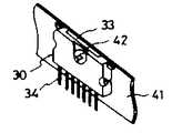
Translated fromKorean제 1 도는 종래의 전력용 반도체장치의 구성을 도시한 투시도.1 is a perspective view showing the structure of a conventional power semiconductor device.
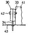
제 2a 도 내지 제 2c 도는 제 1 도에 도시한 전력용 반도체장치의 실장상태를 나타낸 도면.2A to 2C are diagrams showing a mounting state of the power semiconductor device shown in FIG.
제 3a 도 내지 제 3c 도는 본 발명의 1실시예에 따른 전력용 반도체장치의 외관을 나타낸 도면.3A to 3C show an appearance of a power semiconductor device according to an embodiment of the present invention.
제 3d 도는 제 3a 도 ~제 3c 도에 도시한 전력용 반도체장치의 투시도.Fig. 3D or Fig. 3A is a perspective view of the power semiconductor device shown in Figs. 3C.
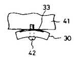
제 4 도는 제 3a 도 내지 제 3d 도에 도시한 전력용 반도체장치에서의 실장시에 발생되는 응력을 나타낸 도면이다.FIG. 4 is a diagram showing stresses generated during mounting in the power semiconductor device shown in FIGS. 3A to 3D.
* 도면의 주요부분에 대한 부호의 설명* Explanation of symbols for main parts of the drawings
1 : 전력용 반도체장치 2 : 마운트 부1: Power semiconductor device 2: Mount
3 : 방열판 4 : 리드단자3: heat sink 4: lead terminal
4' : 내부리드부 5 : 몰딩수지4 ': inner lead part 5: molding resin
6 : 구멍 7 : 절결부6: hole 7: cutout
8 : 지지부분 CP : 반도체칩8: support part CP: semiconductor chip
10 : 홈10: home
[산업상의 이용분야][Industrial use]
본 발명은 전력용 트랜지스터 또는 전력용 반도체집적회로장치(IC)등과 같은 반도체장치에 관한 것으로, 특히 몰드패키지로부터 부분적으로 노출된 방열부를 갖춘 반도체장치에 관한 것이다.BACKGROUND OF THE
[종래의 기술 및 그 문제점][Traditional Technology and Problems]
제 1 도는 종래의 전력용 반도체장치(30)의 구조를 이면(裏面)쪽으로부터 투시하여 도시한 것으로, 이 전력용 반도체장치(30)는 반도체칩(CP)과 몰딩수지(31), 금속제방열판(33) 및 리드단자(34)로 구성되어 있다. 여기서, 상기 방열판(33)에는 아일랜드부(32)가 형성되어 있고, 반도체칩(CP)은 방열판(33)의 표면(表面)쪽에서 상기 아일랜드부(32)에 고정되며, 리드단자(34)가 상기 반도체칩(CP)에 접속된다. 다음, 반도체칩(CP)은 리드단자(34) 및 방열판(33)과 함께 몰딩수지(31)에 의해 밀봉되고, 이때 방열판(33)의 일부는 이면쪽에서 노출되게 되며, 이와 같이 구성된 전력용 반도체장치에는 방열판(33) 및 몰딩수지(31)를 관통하는 구멍(35)이 형성된다.1 is a perspective view showing the structure of a conventional
상기 전력용 반도체장치(30)를 예컨대 전자기기의 방열샤시(41)에 실장하는 경우에는 제 2a 도 및 제 2b 도에 도시된 바와 같이 나사(42)나 클립에 의해 고정됨과 더불어 리드단자(34)의 노출부가 전자기기회로에 접속되게 된다. 즉, 방열판(33)의 이면(裏面)이 방열샤시(41)에 대향하도록 마운트되고, 리드단자(34)는 전자기기회로의 프린트회로기판(43)에 납땜되게 된다.In the case where the
그런데, 상기 전력용 반도체장치(30)에서는 통상 몰딩처리후의 몰딩 수지와 방열판금속의 열적 특성이 달라지기 때문에 제 2c 도에 도시된 바와 같이 구부러짐이 발생되는데, 상기 전력용 반도체장치를 제 3 도에 도시한 상태로 나사(42)나 클립을 이용하여 마운트시키면 이 구부러짐은 작아지게 된다. 그러나, 이때에는 기계적인 스트레스에 의해 반도체칩의 균열이 생기기 쉬울 뿐만 아니라, 상기 전력용 반도체장치(30)의 온도가 사용중에 상승하게 되면 몰딩수지가 열스트레스로 인해 변형되어, 그 응력에 의해 반도체칩의 균열이 발생되는 경우도 있다.However, in the
이와 같은 균열의 원인은 몰딩수지(31)와 방열판(33) 및 반도체칩(CP)을 구성하는 재료상호간의 열팽창률차이에 있기 때문에, 대량 생산공정에서 그 발생율이 0.1% 이하로 되도록 스크리닝하는 것이 곤란하게 된다.The cause of such cracks is the difference in thermal expansion coefficient between the
여기서, 반도체칩의 균열을 방지하기 위해 예컨대 각종 사용재료의 팽창계수를 같게 하는 것을 생각할 수 있지만, 이는 방열판의 방열효율을 현상태로 유지하기가 어렵기 때문에 전력용 반도체장치의 제조공정을 보다 엄격히 관리함으로써 균열의 발생에 대한 여유폭의 최적화를 꾀하고 있다.Here, in order to prevent cracking of the semiconductor chip, it is conceivable to have the same expansion coefficient of various materials used, for example, but it is difficult to maintain the heat dissipation efficiency of the heat sink as it is, and thus strictly control the manufacturing process of the power semiconductor device. By doing so, the margin for the occurrence of cracks is optimized.
[발명의 목적][Purpose of invention]
본 발명은 상기한 점을 감안하여 발명된 것으로, 실장시에 가해지는 응력 또는 온도변화에 기인하는 몰딩수지의 응력에 의해 발생하는 반도체칩의 균열을 방지할 수 있는 반도체장치를 제공함에 그 목적이 있다.SUMMARY OF THE INVENTION The present invention has been made in view of the above point, and an object thereof is to provide a semiconductor device which can prevent cracking of a semiconductor chip caused by stress of a molding resin caused by stress or temperature change applied during mounting. have.
[발명의 구성][Configuration of Invention]
상기 목적을 달성하기 위한 본 발명에 따른 반도체장치는, 반도체칩과, 이 반도체칩의 마운트부 및 반도체장치의 부착부가 일렬로 설치된 중앙영역, 이 중앙영역의 양쪽에서 상기 마운트부 및 부착부와 평행한 방향으로 연장된 복수의 전결부를 갖는 금속방열판, 리드부재 및, 상기 반도체칩과 리드부재의 일부를 방열판과 협력하여 밀봉시키는 몰딩부재로 이루어져 있다.A semiconductor device according to the present invention for achieving the above object includes a semiconductor chip, a central region in which the mount portion of the semiconductor chip and the attachment portion of the semiconductor device are arranged in line, and parallel to the mount portion and the attachment portion in both of the central regions. A metal heat dissipation plate having a plurality of connection parts extending in one direction, a lead member, and a molding member for sealing a part of the semiconductor chip and the lead member in cooperation with the heat dissipation plate.
[작용][Action]
상기와 같이 구성된 본 발명의 반도체장치에 따르면, 방열판의 부착부를 예컨대 클립으로 외부의 방열부재에 설치하였을때 반도체칩쪽으로 향한 응력이 절결부에서 약해지기 때문에 반도체칩의 균열을 방지할 수 있게 된다. 또한, 절결부를 설치한 경우 반도체칩마운트부의 면적을 이 마운트부 이외의 방열판의 면적과 비슷하게 함으로써, 상기 마운트부와 방열판 및 몰딩수지 사이의 열팽창률 차이에 따른 열스트레스에 의해 발생되는 응력의 균형을 맞출 수가 있으므로 반도체칩의 균열이 쉽게 발생하지 않게 된다.According to the semiconductor device of the present invention configured as described above, when the attachment portion of the heat sink is installed to the external heat dissipation member with a clip, for example, the stress toward the semiconductor chip is weakened at the cutout portion, thereby preventing cracking of the semiconductor chip. In addition, when the cutout is provided, the area of the semiconductor chip mount portion is made to be similar to that of the heat sink other than the mount portion, so that the balance of stress caused by thermal stress due to the difference in thermal expansion between the mount portion and the heat sink and the molding resin. Because of this, cracks in the semiconductor chip are not easily generated.
[실시예]EXAMPLE
이하, 제 3a 도 내지 제 3d 도를 참조하여 본 발명의 1 실시예에 따른 전력용 반도체장치에 대해 상세히 설명한다.Hereinafter, a power semiconductor device according to an exemplary embodiment of the present invention will be described in detail with reference to FIGS. 3A to 3D.
이 전력용 반도체장치는 예컨대 오디오기기나 사무자동화기기 또는 공장자동화기기등의 모터제어 등에 이용되는 것으로, 제 3a 도는 전력용 반도체장치의 외관을 나타낸 도면, 제 3b 도는 그 정면도, 제 3c 도는 측면도, 제 3d 도는 상기 전력용 반도체장치를 확대하여 그 내부의 일부를 이면쪽에서 투시한 도면이다.This power semiconductor device is used for motor control of audio equipment, office automation equipment, or factory automation equipment, for example. FIG. 3A or 3B is a front view, 3C is a front view, or 3C is a side view. FIG. 3D is a view in which the power semiconductor device is enlarged and a part of the inside thereof is viewed from the rear side.
상기 전력용 반도체장치는 반도체칩(CP)과 몰딩수지(5), 금속방열판(3) 및 리드단자(4)를 갖추고 있고, 이때 방열판(3)의 일부는 반도체칩(CP)의 마운트부(2 ; 아일랜드부)로 이용된다. 또, 반도체칩(CP)은 방열판(3)의 이면쪽에서 상기 아일랜드부(2)에 마운트되어 리드단자(4)의 내부 리드부(4')에 본딩와이어 등에 의해 전기적으로 접속되며, 이때 리드단자(4)는 상기 방열판(3)과 예컨대 같은 두께로 설정됨과 더불어 전력용 반도체장치의 두께방향으로 방열판(3)과는 다른 위치에 설정되게 된다.The power semiconductor device includes a semiconductor chip CP, a
한편, 상기 아일랜드부(2)와 방열판(3) 및 내부리드부(4')는 패키지를 구성하는 몰딩수지(5)에 의해 밀봉되는데, 이때 방열판(3)의 이면의 일부는 외부에 노출되며, 리드단자(4)와 방열판(3)은 예컨대 같은 두께로 설정되어 전력용 반도체장치의 두께방향으로 단차(段差)를 갖게 된다.Meanwhile, the
구멍(6)은 몰딩수지(5) 및 방열판(3)을 관통하여 형성되어 상기 전력용 반도체장치를 비스 등으로 외부부재에 부착시키는데 이용된다. 또, 상기 전력용 반도체장치의 방열판(3)에는 두개의 절결부(7)가 갖추어져 있고, 이 절결부(7)는 아일랜드부(2)와 구멍(6)이 나란하게 형성된 중앙영역의 양쪽에 인접하게 형성되어 상기 마운트부(21)와 구멍(6)에 평행한 방향으로 연장되어 있다. 즉, 상기 절결부(7)는 방열판(3)의 리드단자(4)쪽을 부분적으로 제거하여 얻어지게 되며, 이 절결부(7)에는 상기 몰딩수지(5)가 채워지게 된다.The
방열판(3) 및 리드단자(4)는 리드프레임(도시되지 않음)의 일부로서, 수지밀봉후에 프레임의 지지부로부터 절단분리된다. 즉, 방열판(3)은 분리되기 전에는 지지부분(8)을 매개하여 프레임에 의해 지지되어 있다.The
또, 반도체칩(CP)은 아일랜드 부(2)에 형성된 두개의 홈(10)으로 둘러싸여 있는데, 안쪽의 홈은 반도체칩(CP)을 납땜으로 마운트부(2)에 마운트시킬 때 흘러나온 납땜을 흡수하는데 이용되고, 바깥쪽의 홈은 몰딩수지(5)와 리드프레임 사이의 틈에서 내부로 들어오는 습기를 방지하는 데 이용된다.In addition, the semiconductor chip CP is surrounded by two
상기 전력용 반도체장치(1)의 실장시에는 방열판(3)의 노출부가 방열용 외부부재(샤시등)에 대향하는 상태로 구멍(6)에 나사를 끼워 결합시키게 되는데, 이 경우 제 4 도에 도시된 바와 같이 종래에는 실선으로 나타낸 화살표방향으로 응력(F)이 발생하여 반도체칩(CP)에 균열이 생길 우려가 있었지만, 본 실시예에서는 빗금부분으로 나타낸 절결부(7)가 형성되어 있기 때문에 상기 응력(F)이 차단되어 점선으로 표시된 바와 같이 아일랜드부(2)로부터 먼 방향으로 응력(F')의 발생위치가 이동하게 된다. 또, 방열판(3)의 전체 폭(ℓ1)에 비해 절결부(7) 상호간의 폭(ℓ2)이 좁기 때문에 실선화살표의 응력(F)보다도 점선화살표의 응력(F')이 작아지게 된다.When mounting the
따라서 본 실시예에 따르면, 상기 응력(F')에 의한 반도체칩(CP)의 균열발생이 거의 확실히 방지되게 된다.Therefore, according to the present embodiment, cracking of the semiconductor chip CP due to the stress F 'is almost certainly prevented.
또한, 수지밀봉후의 사용상태에서의 온도변화에 따른 열스트레스에 대해서는, 아일랜드부(2)에서의 몰딩 수지와의 열팽창차이와 절결부(7)를 갖춘 방열판(3)에서의 몰딩수지와의 열팽창차이의 균형이 이루어지도록 되어 있기 때문에 열스트레스에 의한 반도체칩(CP)의 균열발생도 억제되게 되는 바, 이는 절결부(7)의 존재에 의해 세로방향영역(Y2)을 갖는 방열판(3)의 점유면적이 작아지게 되어 세로방향영역(Y1)을 갖는 아일랜드부(2)의 점유면적과 비슷해지기 때문이다.In addition, for the thermal stress caused by the temperature change in the use state after the resin sealing, the thermal expansion difference with the molding resin in the
이때, 방열판(3)의 절결부(7)의 형성위치는 방열판(3)을 관통하는 나사로 결합시킬 때에 발생하는 응력이 반도체칩에 가해지는 것을 방지할 수 있는 범위내에서 변경되어도 무방하다.At this time, the formation position of the
또, 제 4 도에 도시된 바와 같이 절결부(7)가 리드단자(4)쪽에 형성되는 경우에는 하나의 금속판을 타발(他拔)법으로 형성시킨 리드프레임을 이용할 수도 있다.In addition, when the
[발명의 효과][Effects of the Invention]
이상 설명한 바와 같이 본 발명에 따른 반도체장치에서는 방열판(3)의 일부에절결부(7)를 형성함으로써 실장시에 발생하여 반도체칩에 가해지는 응력을 충분히 감소시킬 수 있게 된다. 따라서, 반도체칩의 균열을 거의 확실하게 방지할 수 있으므로, 종래에 균열발생율을 0.2% 정도까지 밖에 감소시킬 수 없었던 점을 고려하면 그 개선효과가 매우 큰 것이다. 또, 상기 절결부(7)에 의해 방열판(3)과 아일랜드부(2)의 면적이 거의 같아지게 함으로써 반도체장치의 사용상태에서의 열스트레스에 의한 몰딩수지로부터의 응력이 반도체칩에 가해지기가 어렵게되어, 열스트레스에 의한 반도체칩의 균열도 억제되게 된다.As described above, in the semiconductor device according to the present invention, the
더욱이, 상기한 바와 같은 절결부(7)의 형성은 리드프레임을 가공함으로써 간단하고 쉽게 실현될 수 있기 때문에 비용의 상승을 거의 초래하지 않을 뿐만 아니라. 그 크기가 큰 칩에 대해서도 상기와 마찬가지의 효과를 얻을 수 있도록 절결부를 형성하는 리드프레임의 설계가 가능하고, 따라서 리드프레임상에 탑재할 수 있는 반도체칩의 종류가 풍부하게 되어 고성능의 반도체장치를 실현하는 것도 가능하게 된다.Moreover, the formation of the
Claims (7)
Translated fromKoreanApplications Claiming Priority (2)
| Application Number | Priority Date | Filing Date | Title |
|---|---|---|---|
| JP62241366AJPH0828443B2 (en) | 1987-09-26 | 1987-09-26 | Semiconductor device |
| JP62-241366 | 1987-09-26 |
Publications (2)
| Publication Number | Publication Date |
|---|---|
| KR890005864A KR890005864A (en) | 1989-05-17 |
| KR920004640B1true KR920004640B1 (en) | 1992-06-12 |
Family
ID=17073222
Family Applications (1)
| Application Number | Title | Priority Date | Filing Date |
|---|---|---|---|
| KR1019880012330AExpiredKR920004640B1 (en) | 1987-09-26 | 1988-09-23 | Semiconductor devices |
Country Status (3)
| Country | Link |
|---|---|
| US (1) | US4963975A (en) |
| JP (1) | JPH0828443B2 (en) |
| KR (1) | KR920004640B1 (en) |
Families Citing this family (8)
| Publication number | Priority date | Publication date | Assignee | Title |
|---|---|---|---|---|
| IT1239644B (en)* | 1990-02-22 | 1993-11-11 | Sgs Thomson Microelectronics | SUPPLY SUPPLY STRUCTURE SUPPLIED FOR CONTAINERS OF INTEGRATED POWER DEVICES |
| USRE37707E1 (en) | 1990-02-22 | 2002-05-21 | Stmicroelectronics S.R.L. | Leadframe with heat dissipator connected to S-shaped fingers |
| IT1252575B (en)* | 1991-12-20 | 1995-06-19 | Sgs Thomson Microelectronics | MOLD AND PROCESS FOR THE MANUFACTURE OF SEMICONDUCTOR PLASTIC DEVICES, WITH VISIBLE METALLIC DISSIPATOR FOR WELDING CONTROL |
| JP3330459B2 (en)* | 1994-07-04 | 2002-09-30 | 三菱電機株式会社 | Magnetic recording / reproducing device |
| DE19621766A1 (en)* | 1996-05-30 | 1997-12-04 | Siemens Ag | Semiconductor arrangement with plastic housing and heat spreader |
| US6075286A (en)* | 1997-06-02 | 2000-06-13 | International Rectifier Corporation | Stress clip design |
| USD571738S1 (en)* | 2007-06-14 | 2008-06-24 | Philips Lumileds Lighting Company, Llc | LED package |
| WO2012120568A1 (en)* | 2011-03-09 | 2012-09-13 | パナソニック株式会社 | Semiconductor device |
Family Cites Families (4)
| Publication number | Priority date | Publication date | Assignee | Title |
|---|---|---|---|---|
| JPS51118376A (en)* | 1975-04-11 | 1976-10-18 | Hitachi Ltd | Semiconductor unit |
| JPS558913U (en)* | 1978-07-03 | 1980-01-21 | ||
| JPS6018939A (en)* | 1983-07-13 | 1985-01-31 | Hitachi Micro Comput Eng Ltd | Resin-encapsulated semiconductor device |
| US4791472A (en)* | 1985-09-23 | 1988-12-13 | Hitachi, Ltd. | Lead frame and semiconductor device using the same |
- 1987
- 1987-09-26JPJP62241366Apatent/JPH0828443B2/ennot_activeExpired - Lifetime
- 1988
- 1988-09-23KRKR1019880012330Apatent/KR920004640B1/ennot_activeExpired
- 1990
- 1990-01-22USUS07/467,350patent/US4963975A/ennot_activeExpired - Lifetime
Also Published As
| Publication number | Publication date |
|---|---|
| JPS6484651A (en) | 1989-03-29 |
| US4963975A (en) | 1990-10-16 |
| JPH0828443B2 (en) | 1996-03-21 |
| KR890005864A (en) | 1989-05-17 |
Similar Documents
| Publication | Publication Date | Title |
|---|---|---|
| KR970006533B1 (en) | Semiconductor device and manufacturing method | |
| KR101388328B1 (en) | Lead frame based, over-molded semiconductor package with integrated through hole technology(tht) heat spreader pin(s) and associated method of manufacturing | |
| US5397746A (en) | Quad flat package heat slug composition | |
| US6337796B2 (en) | Semiconductor device mount structure having heat dissipating member for dissipating heat generated from semiconductor device | |
| US5444304A (en) | Semiconductor device having a radiating part | |
| US4807018A (en) | Method and package for dissipating heat generated by an integrated circuit chip | |
| KR20030024157A (en) | Power semiconductor module that has three dimensional structure and a method of manufacturing thereof | |
| EP0587294B1 (en) | Semiconductor package | |
| KR920004640B1 (en) | Semiconductor devices | |
| US5093713A (en) | Semiconductor device package | |
| US6758200B2 (en) | Ignition coil driver chip on printed circuit board for plughole coil housing | |
| KR100208634B1 (en) | Surface Mount Semiconductor Devices | |
| JP4331993B2 (en) | Power semiconductor device | |
| US5587883A (en) | Lead frame assembly for surface mount integrated circuit power package | |
| JP4513560B2 (en) | Power module and air conditioner | |
| JP2680110B2 (en) | Package for semiconductor device having heat radiator | |
| KR19980084769A (en) | High heat dissipation package and its manufacturing method | |
| JPS6143857B2 (en) | ||
| JP3284604B2 (en) | Method of manufacturing resin-encapsulated semiconductor device with heat sink | |
| JPH01120856A (en) | Lead frame | |
| US6509637B1 (en) | Low profile mounting of thick integrated circuit packages within low-profile circuit modules | |
| US6979900B2 (en) | Integrated circuit package with integral leadframe convector and method therefor | |
| KR930007171Y1 (en) | Semicondcutor package forming heat emitting bar | |
| JPH11243162A (en) | Ball grid array package provided with expansion buffering insert and manufacture thereof | |
| KR100342811B1 (en) | Area array bumped semiconductor package with chips |
Legal Events
| Date | Code | Title | Description |
|---|---|---|---|
| A201 | Request for examination | ||
| PA0109 | Patent application | St.27 status event code:A-0-1-A10-A12-nap-PA0109 | |
| PA0201 | Request for examination | St.27 status event code:A-1-2-D10-D11-exm-PA0201 | |
| R17-X000 | Change to representative recorded | St.27 status event code:A-3-3-R10-R17-oth-X000 | |
| PG1501 | Laying open of application | St.27 status event code:A-1-1-Q10-Q12-nap-PG1501 | |
| E902 | Notification of reason for refusal | ||
| PE0902 | Notice of grounds for rejection | St.27 status event code:A-1-2-D10-D21-exm-PE0902 | |
| T11-X000 | Administrative time limit extension requested | St.27 status event code:U-3-3-T10-T11-oth-X000 | |
| P11-X000 | Amendment of application requested | St.27 status event code:A-2-2-P10-P11-nap-X000 | |
| P13-X000 | Application amended | St.27 status event code:A-2-2-P10-P13-nap-X000 | |
| G160 | Decision to publish patent application | ||
| PG1605 | Publication of application before grant of patent | St.27 status event code:A-2-2-Q10-Q13-nap-PG1605 | |
| E701 | Decision to grant or registration of patent right | ||
| PE0701 | Decision of registration | St.27 status event code:A-1-2-D10-D22-exm-PE0701 | |
| GRNT | Written decision to grant | ||
| PR0701 | Registration of establishment | St.27 status event code:A-2-4-F10-F11-exm-PR0701 | |
| PR1002 | Payment of registration fee | St.27 status event code:A-2-2-U10-U11-oth-PR1002 Fee payment year number:1 | |
| PR1001 | Payment of annual fee | St.27 status event code:A-4-4-U10-U11-oth-PR1001 Fee payment year number:4 | |
| PR1001 | Payment of annual fee | St.27 status event code:A-4-4-U10-U11-oth-PR1001 Fee payment year number:5 | |
| PR1001 | Payment of annual fee | St.27 status event code:A-4-4-U10-U11-oth-PR1001 Fee payment year number:6 | |
| PR1001 | Payment of annual fee | St.27 status event code:A-4-4-U10-U11-oth-PR1001 Fee payment year number:7 | |
| R18-X000 | Changes to party contact information recorded | St.27 status event code:A-5-5-R10-R18-oth-X000 | |
| PN2301 | Change of applicant | St.27 status event code:A-5-5-R10-R13-asn-PN2301 St.27 status event code:A-5-5-R10-R11-asn-PN2301 | |
| R18-X000 | Changes to party contact information recorded | St.27 status event code:A-5-5-R10-R18-oth-X000 | |
| R18-X000 | Changes to party contact information recorded | St.27 status event code:A-5-5-R10-R18-oth-X000 | |
| PR1001 | Payment of annual fee | St.27 status event code:A-4-4-U10-U11-oth-PR1001 Fee payment year number:8 | |
| PR1001 | Payment of annual fee | St.27 status event code:A-4-4-U10-U11-oth-PR1001 Fee payment year number:9 | |
| PR1001 | Payment of annual fee | St.27 status event code:A-4-4-U10-U11-oth-PR1001 Fee payment year number:10 | |
| R18-X000 | Changes to party contact information recorded | St.27 status event code:A-5-5-R10-R18-oth-X000 | |
| PR1001 | Payment of annual fee | St.27 status event code:A-4-4-U10-U11-oth-PR1001 Fee payment year number:11 | |
| FPAY | Annual fee payment | Payment date:20030530 Year of fee payment:12 | |
| PR1001 | Payment of annual fee | St.27 status event code:A-4-4-U10-U11-oth-PR1001 Fee payment year number:12 | |
| LAPS | Lapse due to unpaid annual fee | ||
| PC1903 | Unpaid annual fee | St.27 status event code:A-4-4-U10-U13-oth-PC1903 Not in force date:20040613 Payment event data comment text:Termination Category : DEFAULT_OF_REGISTRATION_FEE | |
| PC1903 | Unpaid annual fee | St.27 status event code:N-4-6-H10-H13-oth-PC1903 Ip right cessation event data comment text:Termination Category : DEFAULT_OF_REGISTRATION_FEE Not in force date:20040613 | |
| P22-X000 | Classification modified | St.27 status event code:A-4-4-P10-P22-nap-X000 | |
| R18-X000 | Changes to party contact information recorded | St.27 status event code:A-5-5-R10-R18-oth-X000 |