KR910010189B1 - Semiconductor device - Google Patents
Semiconductor deviceDownload PDFInfo
- Publication number
- KR910010189B1 KR910010189B1KR1019880008479AKR880008479AKR910010189B1KR 910010189 B1KR910010189 B1KR 910010189B1KR 1019880008479 AKR1019880008479 AKR 1019880008479AKR 880008479 AKR880008479 AKR 880008479AKR 910010189 B1KR910010189 B1KR 910010189B1
- Authority
- KR
- South Korea
- Prior art keywords
- well
- type
- well region
- memory cell
- region
- Prior art date
- Legal status (The legal status is an assumption and is not a legal conclusion. Google has not performed a legal analysis and makes no representation as to the accuracy of the status listed.)
- Expired
Links
Images


Classifications
- H—ELECTRICITY
- H10—SEMICONDUCTOR DEVICES; ELECTRIC SOLID-STATE DEVICES NOT OTHERWISE PROVIDED FOR
- H10D—INORGANIC ELECTRIC SEMICONDUCTOR DEVICES
- H10D84/00—Integrated devices formed in or on semiconductor substrates that comprise only semiconducting layers, e.g. on Si wafers or on GaAs-on-Si wafers
- H10D84/01—Manufacture or treatment
- H10D84/0123—Integrating together multiple components covered by H10D12/00 or H10D30/00, e.g. integrating multiple IGBTs
- H10D84/0126—Integrating together multiple components covered by H10D12/00 or H10D30/00, e.g. integrating multiple IGBTs the components including insulated gates, e.g. IGFETs
- H10D84/0156—Manufacturing their doped wells
Landscapes
- Semiconductor Memories (AREA)
- Metal-Oxide And Bipolar Metal-Oxide Semiconductor Integrated Circuits (AREA)
Abstract
Translated fromKoreanDescription
Translated fromKorean제1도는 종래의 우물형 구조를 갖춘 반도체장치의 단면도.1 is a cross-sectional view of a semiconductor device having a conventional well structure.
제2a도~제2c도는 본 발명의 제1실시예에 따른 우물형 구조를 갖춘 반도체장치의 제조공정을 나타낸 도면.2A to 2C show a manufacturing process of a semiconductor device having a well structure according to a first embodiment of the present invention.
제3a도∼제3m도는 본 발명의 제1실시예에 따른 우물형 구조를 갖추고 있는 도랑형 DRAM 셀과 그 주변회로가 N형 기판상에 형성되는 경우의 제조공정을 나타낸 단면도.3A to 3M are sectional views showing a manufacturing process in the case where a trench type DRAM cell having a well structure according to the first embodiment of the present invention and a peripheral circuit thereof are formed on an N type substrate.
제4도는 제3m도에 도시된 DRAM이 P형 기판 내에 형성되는 경우를 나타낸 단면도.4 is a cross-sectional view showing a case in which the DRAM shown in FIG. 3m is formed in a P-type substrate.
제5도는 제4도에 도시된 DRAM의 변형예를 나타낸 단면도.FIG. 5 is a sectional view showing a modification of the DRAM shown in FIG.
제6도는 제5도에 도시된 DRAM이 P형 기판 내에 형성되는 경우를 나타낸 단면도.FIG. 6 is a sectional view showing a case where the DRAM shown in FIG. 5 is formed in a P-type substrate.
제7도는 제4도에 도시된 DRAM의 다른 변형예를 나타낸 단면도.FIG. 7 is a cross-sectional view showing another modification of the DRAM shown in FIG.
제8도는 제3m도에 도시된 DRAM의 변형예에 있어서 각종 전원전압이 인가되는 경우의 변형예를 나타낸 단면도.FIG. 8 is a cross-sectional view showing a modification when various power supply voltages are applied in the modification of the DRAM shown in FIG. 3m.
제9a도는 제8도에 도시된 다중전원 DRAM에 저전압 VCC를 공급하기 위한 전압발생회로를 나타낸 도면.FIG. 9A shows a voltage generation circuit for supplying a low voltage VCC to the multi-power DRAM shown in FIG.
제9b도는 제8도에 도시된 다중전원 DRAM에 저전압 VBB를 공급하기 위한 전압발생회로를 나타낸 도면.FIG. 9B shows a voltage generation circuit for supplying a low voltage VBB to the multi-power DRAM shown in FIG.
제10도는 본 발명을 이용하는 DRAM에 적용될 수 있는 도랑형 셀방식의 메모리의 구조를 나타낸 단면도.10 is a cross-sectional view showing the structure of a trench type cell type memory that can be applied to a DRAM using the present invention.
제11도는 본 발명을 이용하는 DRAM에 적용될 수 있는 적층형 셀방식의 메모리의 구조를 나타낸 단면도.Fig. 11 is a cross-sectional view showing the structure of a stacked cell type memory that can be applied to a DRAM utilizing the present invention.
제12도는 본 발명을 이용하는 DRAM에 적용될 수 있는 적층도랑형 셀방식(STT cell type)의 메모리의 구조를 나타낸 단면도.12 is a cross-sectional view showing the structure of a stacked trench type cell type (STT cell type) memory that can be applied to a DRAM using the present invention.
제13도는 본 발명을 이용하는 DRAM에 적용될 수 있는 평판형 셀방식의 메모리의 구조를 나타낸 단면도.Fig. 13 is a sectional view showing the structure of a flat cell type memory that can be applied to a DRAM utilizing the present invention.
제14도는 본 발명에 적용될 수 있는 SRAM의 구조를 나타낸 단면도.14 is a cross-sectional view showing a structure of an SRAM applicable to the present invention.
제15a도∼제15e도는 본 발명이 적용될 수 있는 각종 CMOS 인버터를 각각 나타낸 도면이다.15A to 15E show various CMOS inverters to which the present invention can be applied.
* 도면의 주요부분에 대한 부호의 설명* Explanation of symbols for the main parts of the drawings
301 : 기판 302A,302I,302J,302M : 산화막301:
302F,302G : 필드산화막 302H : 열산화막302F, 302G:
303A,303B,303D,303G : 레지스트막 304A,304B : P형 불순물영역303A, 303B, 303D, 303G:
306D : N형 불순물영역 308 : N형 확산층306D: N-type impurity region 308: N-type diffusion layer
309 : P형 확산층 310 : 도랑309 P-
311 : 캐패시터전극용 확산층 312 : 캐패시터전극311 diffusion layer for
313 : 다결정실리콘층 314 : 알미늄배선층313
P-well-1∼P-well-3 : P형 우물영역P-well-1 to P-well-3: P type well area
N-well-1∼N-well-3 : N형 우물영역N-well-1 to N-well-3: N type well area
본 발명은 우물형 구조를 갖춘 반도체메모리에 관한 것으로, 특히 CMOS 구조의 다이나믹 랜덤 액세스메모리(이하, DRAM이라 약칭함)에 관한 것이다.BACKGROUND OF THE
종래의 DRAM에서는 메모리셀어레이의 주변회로를 구성함에 있어 CMOS 구조를 채택하지 않았으나, 최근에는 CMOS 구조의 DRAM에 대한 요구가 점점 많아지고 있다.Conventional DRAMs do not employ a CMOS structure in configuring peripheral circuits of memory cell arrays, but in recent years, there is an increasing demand for DRAMs having CMOS structures.
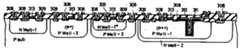
제1도는 CMOS 구조로되어 있는 1트랜지스터/1캐패시터형 DRAM의 일예를 나타낸 단면으로서, 이 제1도에 있어서 참조부호 1은 P형 실리콘기판, 2와 2*는 동일한 제조단계에서 형성되는 P형 우물영역(P-type well region), 3은 N형 우물영역, 4는 캐패시터용 절연막, 5는 캐패시터전극, 6은 트랜지스터의 게이트절연막, 7은 트랜지스터의 게이트전극. 8과 8*는 N+형 확산층(소오스, 드레인), 9는 P+형 확산층(소오스, 드레인), 10은 절연막, 11은 알미늄배선층, A는 메모리셀부, B는 주변회로부를 각각 나타낸다. 여기에서 상기 P형 우물영역(2)은 P형 기판(1)보다 불순물농도가 높게 형성되는 바, 최근에는 소프트에러를 방지하기 위해 고농도불순물의 우물영역 내에 메모리셀을 형성시키는 것이 바람직하다고 알려져 있다.FIG. 1 is a cross-sectional view showing an example of a one-transistor / capacitor type DRAM having a CMOS structure. In FIG. 1,
종래의 메모리장치에서는, 메모리셀이 형성되는 P형 우물영역(2*)의 불순물농도와 주변회로가 형성되는 P형 우물영역(2)의 불순물농도가 동일하게 되어 있으므로, 소프트에러를 억제하기 위해서는 우물영역의 불순물농도를 더 증가시킬 필요가 있었다. 그러나 회로특성이란 관점에서 볼 때, 우물영역의 불순물농도를 과도하게 증가시키는 것은, N+형 확산층(8*)과 P형 우물영역(2*)간의 확산용량을 증가시켜 접합브레이크다운전압(junction break-down voltage)을 저하시키게 됨으로 바람직하지 못하다.In the conventional memory device, the impurity concentration of the P-
한편, IC 내부구조를 미세화시키는 기술이 더욱 더 발전하게 되면, IC의 입출력회로부가 5V의 전압으로 동작한다 하더라도 내부회로는 2∼4V의 전압으로 동작시킬 필요가 있게 된다. 따라서, 전원전압의 차이에 따라 P형 우물영역(2,2*)과 같은 우물영역의 불순물농도를 적절하게 변화시켜 줄 필요가 있으나, 아직까지는 그러한 필요성을 충족시킬만한 구체적인 기술이 개발되어 있지 않다.On the other hand, as the technology for miniaturizing the IC internal structure is further developed, even if the input / output circuit part of the IC operates at a voltage of 5V, it is necessary to operate the internal circuit at a voltage of 2 to 4V. Therefore, it is necessary to appropriately change the impurity concentration of the well region such as the P-type well region (2,2* ) according to the difference in the power supply voltage, but no specific technology has been developed to satisfy such a necessity. .
본 발명은 상기와 같은 실정을 감안하여 발명된 것으로, 각기 다른 불순물농도를 갖는 우물영역을 이용하여 소프트에러와 저항전압간의 상호관계를 개선시킬 수 있는 반도체장치를 제공하고자 함에 그 목적이 있다.SUMMARY OF THE INVENTION The present invention has been made in view of the above circumstances, and an object thereof is to provide a semiconductor device capable of improving a correlation between a soft error and a resistance voltage by using a well region having different impurity concentrations.
상기한 목적을 달성하기 위한 본 발명은, 동일한 도전형이면서 표면불순물농도가 각기 다른 다수의 우물영역을 반도체기판 내에 형성하고, 다수의 우물영역 중에서 표면불순물농도가 가장 높은 우물영역 내에 한 개 또는 다수개의 메모리셀을 형성하는 점에 특징이 있다.According to the present invention for achieving the above object, a plurality of well regions having the same conductivity type and different surface impurity concentrations are formed in a semiconductor substrate, and one or more within the well region having the highest surface impurity concentration among the plurality of well regions. It is characterized in that it forms four memory cells.
더욱이 본 발명은, 제1도전형(P형) 제1우물영역들을 반도체기판(P 또는 N형)내에 형성하고, 제1도전형(P형) 또는 제2도전형(N형) 제2우물영역(한개 또는 다수개)을 형성하기 위해 제2도전형(N형) 제1우물영역을 상기 제1도전형 제1우물영역들 중에서 선택된 하나 또는 그 이상의 우물영역 내에 형성하며, 다수의 우물영역 중에서 표면불순물농도가 가장 높은 우물영역 내에 한개 또는 다수개의 메모리셀을 형성하는 점에 특징이 있다.Furthermore, in the present invention, the first conductive type (P type) first well regions are formed in the semiconductor substrate (P or N type), and the first conductive type (P type) or the second conductive type (N type) second well A second conductive type (N-type) first well region is formed in one or more well regions selected from the first conductive type first well regions to form a region (one or more), and a plurality of well regions Among them, one or more memory cells are formed in the well region having the highest surface impurity concentration.
따라서 본 발명의 기본적인 특징은, 제1도전형 불순물(P형)을 제2도전형 불순물(N형)과 부분적으로 중화시키기 위해 하나 또는 다수개의 선택된 우물영역(제1도전형)내에 제2도전형 우물영역을 형성시킴으로써, 반도체기판 내에 형성되는 여타 제1도전형 우물영역(P++, 하나 또는 다수개)보다 낮은 불순물농도를 갖는 제1도전형 우물영역(P+)을 제공할 수 있게 된다.Thus, the basic feature of the present invention is that the second conductivity within one or a plurality of selected well regions (first conductivity type) to partially neutralize the first conductivity type impurity (type P) with the second conductivity type impurity (type N). By forming the type well region, it is possible to provide the first conductive type well region P+ having a lower impurity concentration than the other first conductive well regions P++ formed in the semiconductor substrate. do.
또한, 본 발명의 기본적인 특징은, 제1도전형 불순물을 하나 또는 그 이상의 제1도전형 저농도 우물영역(P,P+)내에 도우프시켜 하나 이상의 제1도전형 고농도 우물영역(P++)을 형성시킨다는 점에 있다.In addition, a basic feature of the present invention is that one or more of the first conductivity type high concentration well regions P++ is doped by doping the first conductivity type impurities into one or more of the first conductivity type low concentration well regions P and P+ . In that it forms.
상기 방식을 통하여 3가지 형태의 각기 다른 제1도전형 영역(P형)을 얻게 되는 바, 즉 반도체기판(P)자체와, 이 반도체기판 내에 형성되는 제1도전형 우물영역(P++) 및, 제2도전형 불순물의 도우프에 의해 불순물 농도가 저하된 제1도전형 우물영역(P+)등을 얻게 된다. 더욱이, 두가지 다른 형태의 제2도전형(N형) 우물영역을 형성하는 경우에는, 각기 다른 정도의 불순물농도를 갖는 여러 가지의 제1도전형 우물영역을 얻을 수도 있게 된다.Through this method, three types of different first conductive region P-types are obtained, that is, the semiconductor substrate P itself, and the first conductive well region P++ formed in the semiconductor substrate. And the first conductivity type well region P+ having the impurity concentration lowered by the doping of the second conductivity type impurity. Further, in the case of forming two different types of second conductivity type (N-type) well regions, it is possible to obtain various first conductivity type well regions having different impurity concentrations.
이와 같은 구조를 DRAM에 적용시키는 경우에는, 가장 높은 불순물농도를 갖는 제1도전형 우물영역에 메모리셀을 형성시키기는 것이 바람직한 바, 이것은 메모리캐패시터내의 누설전류가 더 낮아져야 되고 소프트에러가 최소화되어야 할 필요가 있기 때문이다.When such a structure is applied to a DRAM, it is desirable to form a memory cell in the first conductivity type well region having the highest impurity concentration, which requires lower leakage current in the memory capacitor and minimizes soft errors. Because you need to.
더욱이, 본 발명에서는 이온주입단계를 다수의 부단계를 나누어 반도체기판의 각 부분에 도우프되는 불순물의 양을 조절함으로써 불순물농도의 선택정도를 다양하게 해서 다수의 우물영역을 형성시킬 수 있게 된다.Furthermore, in the present invention, the ion implantation step is divided into a plurality of sub-steps to adjust the amount of impurities doped to each part of the semiconductor substrate, thereby making it possible to form a plurality of well regions by varying the degree of selection of impurity concentration.
이하, 예시도면을 참조하여 본 발명의 실시예를 상세히 설명한다.Hereinafter, exemplary embodiments of the present invention will be described in detail with reference to the accompanying drawings.
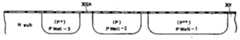
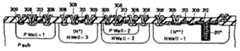
제2a도∼제2c도는 본 발명의 제1실시예에 따른 우물형 구조를 갖춘 반도체장치의 제조공정을 나타낸 단면도로서, 우선 제2a도에 나타낸 바와 같이 DRAM내에 셀영역(A)의 P형 제1우물영역(102-1)을 형성시키기 위해 배치된 P형 반도체기판(101)의 일부에 포토리소그라피법(photo-lithographic method)으로 보론을 이온주입시킨다(이 경우, 이온주입조건은 도우즈량이 2×1014cm-2, 가속전압이 100KeV이다).이와 동시에 주변회로부(B)의 P형 제2우물영역(102-2)을 형성하기 위해 배치된 반도체기판(101)의 일부에도 보론을 이온주입시킨다. 그후, 반도체구조물을 1190℃의 온도와 N2가스분위기에서 6시간정도 열처리하여 P형 우물영역(102-1,102-2)을 형성하게 되는 바, 제2a도는 이러한 열처리후에 얻어진 반도체구조를 나타낸 것이다. 이 제2a도에서 XXX는 이온주입된 보론을 나타낸다.2A to 2C are cross-sectional views showing the manufacturing process of the semiconductor device having the well-type structure according to the first embodiment of the present invention. First, as shown in FIG. 2A, the P-type material of the cell region A in the DRAM is shown. 1 Boron is ion-implanted into a portion of the P-
다음에는 도우즈량 5×1013cm-3와 가속전압 100KeV의 조건에서 레지스트막(103; resist film)을 이용하여 N형 제1우물영역(106)과 P형 제2우물영역(102-2)의 내부영역(105)을 형성하기 위해 배치된 부분에 인(104:P)을 이온주입시킨다. 그후, 반도체구조물을 1190℃의 온도와 N2가스분위기에서 4시간동안 2차로 열처리한다. 그 결과, 표면불순물농도가 5×1017cm-2인 P형 제1우물영역(107; P++)이 셀영역(A)내에 형성되고, 표면불순물농도가 2×1017cm-2인 P형 제2우물영역(105; P+)이 주변회로부(B)의 N채널영역 내에 형성되게 된다.Next, the N-type
그 다음에는 캐패시터절연막(108)과 축적전극(109; 다결정실리콘), 기록/독출용 트랜지스터의 N+형 확산층(110) 및 게이트전극(111; 다결정실리콘), 비트선용 배선층(112; 알미늄)을 셀영역(A)내에 형성하고, 더욱이 N채널 트랜지스터의 게이트전극(113; 다결정실리콘)과 P채널 트랜지스터의 게이트전극(114; 다결정실리콘), 확산영역(115,116), 각 전극에 대한 인출배선층(117; 알미늄)등을 행/열디코더와 센스앰프같은 주변회로용의 P형 제2우물영역(105)과 N형 제1우물영역(106)내에 형성함으로써, 제2c도에 나타낸 것과 같은 CMOS DRAM을 완성하게 된다.Next, the
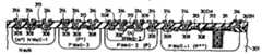
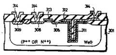
제3a도∼제3m도는 본 발명의 제1실시예에 따른 우물형 구조를 갖추고 있는 도랑형 DRAM 셀과 그 주변회로가 N형 기판상에 형성되는 경우의 제조공정을 나타낸 단면도로서, 이하 그 공정을 상세히 설명한다.3A to 3M are sectional views showing a manufacturing process in the case where a trench type DRAM cell having a well-type structure according to the first embodiment of the present invention and a peripheral circuit are formed on an N-type substrate. It will be described in detail.
우선, 제3a도에 나타낸 바와 같이 1000Å 두께의 SiO2산화막(302A)으로 덮여 있는 N형 기판(301)의 소정부분 상에 레지스트막(303A)을 형성(패터닝)한 다음, P형 불순물인 보론을 도우즈량 2×1013cm-2과 가속전압 1000KeV의 조건에서 레지스트막(303A)의 개구부를 통해 이온주입시킨다. 이러한 이온주입공정의 결과로 레지스트막(303A)의 개구부 밑에 위치하는 N형 기판(301)의 일부에 P형 불순물영역(304A)이 형성되게 된다.First, as shown in FIG. 3A, a resist
그후, 제3b도에 나타낸 바와 같이 새로운 레지스트막(303B)을 개구부와 함께 형성하고, 3×1013cm-2의 도우즈량과 100KeV의 가속전압 하에 보론을 레지스트막(303B)의 개구부를 통하여 이온주입시킨다. 이러한 이온주입공정의 결과, P형 불순물영역(304A)에 덧붙여 P형 불순물영역(304B)과 P형 불순물영역(304A+304B)이 N형 기판(301)내에 형성되게 된다.Thereafter, as shown in FIG. 3B, a new resist film 303B is formed with the openings, and boron is ionized through the openings of the resist film 303B under a dose amount of 3x1013 cm-2 and an acceleration voltage of 100 KeV. Inject. As a result of this ion implantation process, in addition to the P-
그 다음에는 레지스트막(303B)을 제거하고, 반도체구조물을 1190℃의 온도와 N2가스분위기에서 6시간동안 열처리한다. 그 결과, P형 불순물영역(304A,304B,304A+304B)이 열적으로 확산(P형 우물영역의 drive-in 확산)되어 제3c도에 나타낸 바와 같이 낮은 불순물농도(P)의 P-well-2와 중간불순물농도(P+)의 P-well-3 및 높은 불순물농도(P++)의 P-well-1이 형성되게 된다.Then, the resist film 303B is removed, and the semiconductor structure is heat-treated for 6 hours at a temperature of 1190 占 폚 and an N2 gas atmosphere. As a result, the P-
그후, 제3d도에 나타낸 바와 같이, 새로운 레지스트막(303D)을 개구부와 함께 형성한 다음, 인(N형 불순물)을 3×1013cm-2의 도우즈량과 160KeV의 가속전압 하에 레지스트막(303D)의 개구부를 통해 이온주입시킨다. 이러한 이온주입공정의 결과로 N형 불순물영역(306D)이 N형 기판(301)과 P-well-2내에 형성되게 된다.Thereafter, as shown in FIG. 3D, a new resist film 303D is formed with an opening, and then phosphorus (N-type impurity) is formed under a dosing amount of 3 x 1013 cm-2 and an acceleration voltage of 160 KeV. Ion implantation is carried out through the opening of 303D). As a result of this ion implantation process, the N-
다음에는 레지스트막(303D)을 제거하고, 반도체구조물을 1190℃의 온도와 N2가스분위기에서 4시간동안 열처리한다. 그 결과, N형 불순물영역(306D)이 열적으로 확산(N형 우물영역의 drive-in 확산)되어 제3e도에 나타낸 바와 같이 N형 기판(301)내에 N-well-1과 P-well-2내의 N-well-2가 형성되게 된다.Next, the resist film 303D is removed and the semiconductor structure is heat-treated for 4 hours at a temperature of 1190 ° C and an N2 gas atmosphere. As a result, the N-
상기한 열적인 확산공정에 있어서, N-well-2의 N형 불순물은 P-well-2의 P형 불순물에 의해 부분적으로 중화되게 된다. 따라서, N-well-2의 불순물농도(N)가 N-well-1의 불순물농도(N+)보다 낮게 설정되게 된다.In the thermal diffusion process described above, the N-type impurity of N-well-2 is partially neutralized by the P-type impurity of P-well-2. Therefore, the impurity concentration N of N-well-2 is set lower than the impurity concentration N+ of N-well-1.
다음에는 제3f도에 나타낸 바와 같이 산화막(302A)을 제거하고 필드산화막(302F)을 형성한다. 이어서, 두꺼운 레지스트막(302G)을 반도체구조물상에 형성하고, 제3g도에 나타낸 바와 같이 반응성 이온엣칭법(RIE법)이나 레이저빔을 사용하여 P-well-1의 소정부분에 메모리셀 캐패시터용 도랑(310; trench)을 형성한다. 그후, 200Å두께의 열산화막(SiO2)을 실리콘기판(레지스트막이 제거된 상태)상에 형성한다.Next, as shown in FIG. 3F, the
다음으로, 상기 도랑(310)과 그 주변의 열산화막을 엣칭하여 도랑(310)주위의 필드산화막(302G)을 선택적으로 제거하며, N형 불순물확산용으로 도우프된 다결정실리콘층(도시하지 않았음)을 반도체구조물 상에 형성한다. 그후, 반도체구조물을 열처리하여 도우프된 다결정실리콘층으로부터 도랑(310)의 표면영역으로 N형 불순물을 확산시킴으로써, 제3h도에 나타낸 바와 같이 캐패시터전극용 확산층(311)을 형성한다. 상기 도우프된 다결정실리콘층은 확산층(311)이 형성된 후에 제거된다.Next, the
다음에는 제3i도에 나타낸 바와 같이, 열산화막(302H)을 제거한 후 확산층(311)을 갖춘 반도체기판(301)상에 100Å두께의 대단히 얇은 SiO2막(302I)을 형성하게 되는데, 이 산화막(302I)은 메모리캐패시터의 유전체로서 사용되는 것이다. 또한, 확산층(311)위에 배치된 유전산화막(302I)의 일부와 함께 도랑(310)의 내부표면과 그 주위에 캐패시터전극용 다결정실리콘층(312)을 형성한다. 이어서, 소정두께(예컨대 200Å)의 산화막(302J)이 기판(301)상에 형성될 때까지 기판표면을 산화시키게 되고, 그후 제3j도에 나타낸 바와 같이 게이트전극으로 사용되는 다결정실리콘층(313)을 산화막(302J)상에 형성한다.Next, as shown in FIG. 3I, after removing the
다음에는 제3k도에 나타낸 바와 같이 소오스와 드레인영역을 형성하는 N형 확산층(308)을 레지스트막(도시되지 않았음)에 의해 P-well-1과 P-well-3의 각 전극(313)의 양쪽에 형성하고, 더욱이 N-well-1과 N-well-2의 종단부에 N형 확산층(308)을 형성한다.Next, as shown in FIG. 3k, each of the
그후, 제3l도에 나타낸 바와 같이 레지스트막(도시되지 않았음)을 사용하여 P-well-1∼P-well-3의 종단부에 P형 확산층(309)을 형성하고, 더욱이 N-well-1과 N-well-2의 각 전극(313)의 양측에 소오스 및 드레인 영역을 형성하는 P형 확산층(309)을 형성한다.Thereafter, as shown in FIG. 3L, a P-
다음에는 제3m도에 나타낸 바와 같이 기판(301)의 전표면 상에 두꺼운 SiO2막(302M; 제2산화막)을 형성하고. 이 제2산화막(302M)의 소정부분을 엣칭하여 개구부를 형성하며, N형 확산층(308)과 P형 확산층(309) 및 캐패시터전극(312)의 접속부분에 개구부를 통하여 알미늄배선층(314)을 선택적으로 형성한다.Next, as shown in FIG. 3m, a thick SiO2 film 302M (second oxide film) is formed on the entire surface of the
제3m도에 있어서, 전원전압변환회로를 구성하는 P채널 트랜지스터와 입출력회로, 입력보호회로 등은 N-well-1내에 향성되고, 센스앰프 등을 구성하는 P채널 트랜지스터는 N-well-2내에 형성된다. 또한, 메모리셀과 센스앰프를 구성하는 N채널 트랜지스터, 워드선구동기 등은 P-well-1∼P-well-3중에서 불순물농도가 가장 높은 영역, 즉 P-well--1내에 형성된다. 더욱이 주변회로 등은 P-well-2내에 형성된다.In FIG. 3m, the P-channel transistors, the input / output circuits, the input protection circuits, etc., which constitute the power supply voltage conversion circuit, are directed to the N-well-1, and the P-channel transistors, which constitute the sense amplifier, are placed in the N-well-2. Is formed. Further, the N-channel transistors, word line drivers, and the like constituting the memory cell and the sense amplifier are formed in the region with the highest impurity concentration among the P-well-1 to P-well-3, that is, P-well-1. Furthermore, peripheral circuits and the like are formed in P-well-2.
상기한 구성에 있어서, N-well-2는 P-well-2에 의해 N-well-1과 분리되어 있기 때문에 N-well-1과 N-well-2에 인가되는 전압은 각각 다른 전압레벨로 설정할 수 있게 된다. 또한, P-well-1(P++)보다 불순물농도가 높은 N형 우물영역을 도면에는 도시되지 않은 어떤 부위에 형성시킬 수도 있다.In the above configuration, since the N-well-2 is separated from the N-well-1 by the P-well-2, the voltages applied to the N-well-1 and the N-well-2 have different voltage levels. It can be set. Further, an N-type well region having a higher impurity concentration than P-well-1 (P++ ) may be formed at any portion not shown in the drawing.
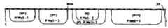
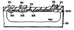
제4도는 제3m도에 도시된 DRAM이 P형 기판에 형성된 경우를 나타낸 단면도로, 제3m도에서는P-well-2 내에 N-well-2가 형성되어 있지만, 제4도에서는 N-well-3내에 P-well-2가 형성되어 있다.FIG. 4 is a cross-sectional view showing a case in which the DRAM shown in FIG. 3m is formed on the P-type substrate. In FIG. 3m, N-well-2 is formed in P-well-2. In FIG. P-well-2 is formed in three.
제5도는 제4도에 도시된 DRAM의 변형예를 나타낸 도면으로, 이 제5도에 있어서는 메모리셀용 P-well-1이 N-well-2내에 형성되고. P-well-2내의 N-well-1*은 N-well-1과 동일한 단계에서 형성되거나 N-well-1의 형성단계 직후에 즉시 형성된다.FIG. 5 is a diagram showing a modification of the DRAM shown in FIG. 4. In FIG. 5, a memory cell P-well-1 is formed in N-well-2. N-well-1* in P-well-2 is formed at the same stage as N-well-1 or immediately after formation of N-well-1.
제6도는 제5도에 도시된 DRAM의 P형 기판에 형성되는 경우를 나타낸 단면도로, 이 제6도에 도시된 구조물은 불순물의 도전형이 P형에서 N형으로 바뀌거나 이와 반대로 바뀌는 것을 제외하고는 제5도에 도시된 것과 유사하다.FIG. 6 is a cross-sectional view showing a case of forming the P-type substrate of the DRAM shown in FIG. 5, except that the conductivity type of the impurity is changed from P-type to N-type or vice versa. Is similar to that shown in FIG.
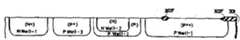
제7도는 제4도에 도시된 DRAM의 또 다른 변형예를 나타낸 도면으로, 이 실시예에서 N-well-1의 불순물농도(N++)는 가장 높게 되어 있고, 메모리셀은 이 N-well-1내에 형성되어 있다. 또한, DRAM의 주변회로는 상기 N-well-1보다 불순물농도가 낮은 N-well-2내에 형성되어 있다. 여기서, 본 실시예의 상기 설명에서 불순물농도가 가장 높다는 것은 N형 불순물에 관련된 것이므로, 예컨대 P-well-1은 N-well-1의 N형 불순물농도보다 높은 P형 불순물농도를 가지도록 형성될 수도 있다.FIG. 7 is a view showing another modified example of the DRAM shown in FIG. 4. In this embodiment, the impurity concentration (N++ ) of N-well-1 is the highest, and the memory cell has this N-well. It is formed within -1. In addition, the peripheral circuit of the DRAM is formed in the N-well-2 having a lower impurity concentration than the N-well-1. Here, the highest impurity concentration in the above description of this embodiment relates to the N-type impurity, so for example, P-well-1 may be formed to have a P-type impurity concentration higher than the N-type impurity concentration of N-well-1. have.
제8도는 제3m도에 도시된 DRAM의 변형예를 나타낸 단면도로, 이 실시예에서는 각종 전원전압이 인가되도록 되어 있는 바, 즉 외부전원전압(Ext, VCC; +5V)은 입출력회로를 구성하는 P채널 트랜지스터 등이 형성되는 N-well-1에 인가되고, 제9a도에 도시된 전압발생회로와 같은 수단에 의해 생성되는 내부전원전압(Int.VCC; +4V)은 P-well-2내에 형성된 N-well-2에 인가된다. 이 제8도의 구조물에 있어서, N-well-2와 P-well-2간의 PN 접합은 상기 Ext.VCC(+5V)와 Int.VCC(+4V)간의 전위차에 의해 역으로 바이어스되게 되는 바, 그에 따라 N-well-2는 P-well-2로부터 전기적으로 분리되게 된다. 따라서, Ext.VCC(+5V)는 비교적 높은 동작전압을 필요로 하는 입출력회로에 인가될 수 있고, 이와 동시에 Int.VCC(+4V 또는 그 이하)는 낮은 동작전압 하에서 동작할 필요가 있는 내부회로에 인가될 수 있게된다. 더욱이, P-well-1내의 메모리셀에 인가되는 낮은 부전압(Int.VBB; -2V)은 예컨대 제9b도에 도시된 전압발생회로 같은 것에서 생성될 수 있다. P-well-2와 N형 기판간의 PN 접합은 EXT.VCC(+5V) 또는 Int.VCC(+4V)와 Int.VBB(-2V)간의 전위차에 의해 역으로 바이어스되게 되는 바, 그에 따라 낮은 부전압(Int,VBB; -2V)이 사용될 수 있게 된다. 다시 말하면, 각종 레벨의 바이어스전압을 각 우물영역에 인가할 수 있게 되어 우물영역 내에 형성된 트랜지스터의 소오스-드레인 전압을 자유롭게 설정할 수 있게 된다.FIG. 8 is a cross-sectional view showing a modified example of the DRAM shown in FIG. 3m. In this embodiment, various power supply voltages are applied, that is, the external power supply voltages Ext, VCC (+ 5V) constitute an input / output circuit. The internal power supply voltage (Int.VCC; + 4V) applied to the N-well-1 in which a P-channel transistor or the like is formed and generated by the same means as the voltage generating circuit shown in Fig. 9A is stored in P-well-2. Is applied to the formed N-well-2. In the structure of FIG. 8, the PN junction between N-well-2 and P-well-2 is reversely biased by the potential difference between Ext.VCC (+ 5V) and Int.VCC (+ 4V). As a result, N-well-2 is electrically isolated from P-well-2. Thus, Ext.VCC (+ 5V) can be applied to an input / output circuit requiring a relatively high operating voltage, while Int.VCC (+ 4V or less) is an internal circuit that needs to operate under a low operating voltage. Can be applied to. Furthermore, the low negative voltage (Int. VBB; -2V) applied to the memory cell in P-well-1 can be generated, for example, in the voltage generation circuit shown in FIG. 9B. The PN junction between P-well-2 and N-type substrate is reversely biased by the potential difference between EXT.VCC (+ 5V) or Int.VCC (+ 4V) and Int.VBB (-2V). Negative voltages Int, VBB; -2V can be used. In other words, various levels of bias voltage can be applied to each well region, so that the source-drain voltage of the transistor formed in the well region can be freely set.
더욱이, 제15a도∼제15e도에 도시된 CMOS 인버터는 본 발명의 반도체장치에 적용될 수 있는 것이다.Further, the CMOS inverter shown in Figs. 15A to 15E can be applied to the semiconductor device of the present invention.
한편, 위에서 언급된 제9a도와 제9b도의 회로는 하기 논문에 게재되어 있는 것이다.Meanwhile, the circuits of FIGS. 9A and 9B mentioned above are disclosed in the following paper.
1986년 IEEE 국제고체회로회의IEEE International Solid State Conference, 1986
ISSCC 86/1986년 2월 21일 금요일ISSCC 86/1 Friday, February 21,986
강좌 XIX:다이내믹 램 272∼273페이지Course XIX: Dynamic RAM Pages 272-273
FAN 19.7:실험적인 4메가비트 CMOS DRAM 후루야마 도오루, 오사와 다카시, 와타나베 요지, 이시우치 히데미, 다나카 다케시, 오우치 가즈노리, 단고 히로유키, 나토리 겐지, 오자와 오사무, 일본국 가와사키시 도시바 반도체장치 엔지니어링 연구소/VLSI 리서치 센터FAN 19.7: Experimental 4 Megabit CMOS DRAM Toru Furuyama, Takashi Osawa, Yoshi Watanabe, Hideyoshi Ishiuchi, Takeshi Tanaka, Kazunori Ouchi, Hiroyuki Dango, Kenji Natori, Osamu Ozawa, Toshiba Semiconductor, Japan Engineering Lab / VLSI Research Center
제10도는 본 발명을 이용한 DRAM에 적용될 수 있는 도랑형 셀방식의 메모리의 구조를 나타낸 도면으로, 이 구조물은 제3m도와 유사하다[그러나 기판(301)의 도전형은 P형이나 N형이 될 수 있다]. 여기에서 게이트전극(313)은 메모리셀의 워드선으로 사용되고, 제10도의 좌측에 설치되어 있는 확산영역(308)에 접속된 알미늄배선층(314)은 메모리셀의 비트선으로 사용된다. 기타 다른 구조로된 도랑형 메모리의 예들은 다음의 미국특허명세서에 게재되어 있다.FIG. 10 is a view showing the structure of a trench type cell type memory applicable to DRAM according to the present invention, which is similar to that of FIG. 3M. However, the conductivity type of the
미국특허 번호 제4,672,410호U.S. Patent No. 4,672,410
발명자; 미우라씨 등inventor; Miura
발간일; 1987년 1월 9일Publication date; January 9, 1987
명칭; 각 메모리셀을 둘러싸는 도랑을 갖춘 반도체 메모리장치designation; Semiconductor memory device with trench surrounding each memory cell
미국특허 번호 제4,673,962호U.S. Patent No. 4,673,962
발명자; 채터지씨 등inventor; Chattersey, etc.
발간일; 1987년 1월 16일Publication date; January 16, 1987
명칭; 수직형 DRAM셀과 그 제조방법designation; Vertical DRAM Cell and Manufacturing Method
여기에서 상기 미국특허명세서에 게재된 내용들은 본 발명과 연관되어 있음에 유의해야 한다.It should be noted that the contents disclosed in the US patent specification are related to the present invention.
제11도는 본 발명을 이용한 DRAM에 적용될 수 있는 적층형(stacked type) 셀방식의 메모리구조를 나타낸 도면으로, 이 적층형 셀방식의 메모리에 있어서 메모리캐패시터는, 수십 Å 두께의 오목포트형(concave pot type) 다결정실리콘 축적노오드(312B)와, 산화막(유전체)을 매개하여 이 축적노오드(312B)의 오목부에 맞물리는 블록형 캐패시터전극(312A)으로 구성되어 있다.FIG. 11 is a diagram showing a stacked cell type memory structure applicable to DRAM according to the present invention. In the stacked cell type memory capacitor, a memory capacitor is a concave pot type having a thickness of several tens of micrometers. A polysilicon storage node 312B and a block-
제12도는 본 발명을 이용한 DRAM에 적용될 수 있는 적층형 도랑셀방식(stacked trench cell type; STT 셀방식)의 메모리구조를 나타낸 도면으로, 이 STT 구조는 제11도에 도시된 적층형 셀의 구조를 제10도의 도랑구조에 적용시킴으로써 달성된다. 본 발명에 사용되는 이러한 STT 구조는 대규모 기억용량의 DRAM, 예컨대 16메가비트의 DRAM에 적합하다.FIG. 12 is a view showing a stacked trench cell type (STT cell type) memory structure applicable to DRAM according to the present invention, and this STT structure removes the structure of the stacked cell shown in FIG. It is achieved by applying it to a 10 degree trench. This STT structure used in the present invention is suitable for large-capacity DRAM, such as 16 megabit DRAM.
제13도는 본 발명을 이용한 DRAM에 적용될 수 있는 평판형 셀방식의 메모리구조를 나타낸 도면으로, 이 구조는 제2c도의 영역(A)내에 있는 셀의 구조에 대응되는 것이다.FIG. 13 shows a planar cell type memory structure applicable to DRAM according to the present invention, which corresponds to the structure of a cell in the area A of FIG.
제14도는 본 발명에 적용될 수 있는 CMOS의 구조를 나타낸 도면으로, 이 실시예에 있어서 셀트랜지스터의 드레인결선층은 저저항의 제1다결정실리콘층(312F; 내부결선층用)과 고저항의 제2다결정실리콘층(312G; 부하저항用)으로 된 2층구조의 형태로 형성된다.14 is a view showing a structure of a CMOS that can be applied to the present invention. In this embodiment, the drain wiring layer of the cell transistor is formed of a low resistance first
이하의 간행물에 게재되는 바이폴라-CMOS 기술은 본 발명에 이용될 수 있는 종래의 메모리셀기술로 적용될 수 있는 것들이다.The bipolar-CMOS technology disclosed in the following publications are those that can be applied to the conventional memory cell technology that can be used in the present invention.
고체회로의 IEEE 학회지IEEE Journal of Solid State Circuits
VOL.SC-22, No.5, 1987년 10월 간행Published in VOL.SC-22, No.5, October 1987
제목; 실험적인 1메가비트 BiCMOS DRAMtitle;
657∼662페이지Pages 657-662
기츠가와 고로, 호리 료이치, 가와지리 요시키, 와타나베 다카오, 가와하라 다카유키, 이토오 기유, 고바야시 유타카, 오오야시 마사유키, 아사야마 교이치로, 이케다 다카히데, 가와모토 히로시.Katsugawa Koro, Hori Ryoichi, Kawajiri Yoshiki, Watanabe Takao, Kawahara Takayuki, Itou Kiyu, Kobayashi Yutaka, Oyashi Masayaki, Asayama Kyichiro, Takada Ikeda, Hiroshi Kawamoto.
408- IEDM86408- IEDM86
제목; 고속 VLSI用의 개선된 BiCMOS 기술title; Improved BiCMOS technology for high speed VLSI
408∼411페이지Pages 408 to 411
이케다.T*, 니카노.T, 몸마.N, 미야타.K, 히구치.H**, 오다카.M*, 오기우에.K*, 일본국 319-12 이바라키 히다치시 구지정 4029 히다치연구소Ikeda .T*, your Kano .T, momma .N, Miyata .K, Higuchi .H**, Oda car .M*, come Yiwu .K*, Hitachi City, Ibaraki, Japan 319-12 nine designated 4029 Hitachi Research Institute
* 일본국 198 도쿄 오우메시 이마이정 2326 장치개발센터* Device Development Center, 2326, Imai-cho, Oume-shi, 198, Japan
**일본국 185 도쿄 고쿠분지시 중앙연구소 히다치 Ltd.** Hitachi Ltd., Kokubunji, Tokyo, 185, Japan
802- IEDM86802- IEDM86
제목; 고속 메가비트 DRAM용 바이폴라 CMOS의 합체된 구조title; Integrated Structure of Bipolar CMOS for High Speed Megabit DRAM
802∼804페이지Pages 802 to 804
고바야시.Y. 오오하야시.M, 아사야마.K, 이케다.T*, 호리.R**, 이토.K**, 일본국 319-12 지바라키 히다치시 히다치 Ltd., 히다치연구소Kobayashi. Y. Oh Hayashi .M, Mt. Asa .K, Ikeda .T*, Hori .R**, Ito .K**, Chiba, Japan 319-12 Rocky Hitachi City Hitachi Ltd., Hitachi Research Institute
*일본국 198 도쿄 오우메시 히다치 Ltd., 장치개발센터* Device Development Center, Hitachi Ltd., Tokyo Ume City, 198, Japan
**일본국 185 도쿄 고쿠분지 히다치 Ltd., 중앙연구소** Japan 185 Tokyo Kokubunji Hitachi Ltd., Central R & D Center
본 발명의 반도체기억장치와 유사하게 보이면서도 실질적으로는 다른 바이폴라장치는 다음의 기술서적에 게재되어 있다.Bipolar devices, which look similar to the semiconductor memory device of the present invention but are substantially different, are described in the following technical book.
제목; 반도체장치의 물리학과 기술title; Physics and Technology of Semiconductor Devices
209페이지Page 209
저자; 에이. 에스 그로브author; a. S Grove
서클리, 캘리포니아대학, 팔로알토, 훼어차일드반도체Circleley, University of California, Palo Alto, Fairchild Semiconductor
뉴욕, 런던, 시드니, 죤 와일리 앤드 손즈 Inc.New York, London, Sydney, John Wiley & Sons Inc.
제목; 반도체장치의 물리학 제2판title; Physics of Semiconductor Devices, Second Edition
192∼197페이지Pages 192-197
저자; 에스. 엠. 스제author; s. M. Seze
뉴저지, 머레이 힐, 벨연구소 인코포레이티드New Jersey, Murray Hill, Bell Labs Incorporated
뉴욕.치체스터.브리스베인.토론토.싱가포르, 존 와일리 앤드 손즈New York, Chichester, Brisbane, Toronto, Singapore, John Wiley & Sons
와일리-인터사이언스 퍼블리케이션Wiley-Interscience Publishing
일반적으로, 바이폴라장치는 고농도불순물영역과 저농도불순물영역을 포함하지만, 그 영역들은 본 발명의 고농도불순물(P++)의 우물영역 및 저농도불순물(P+,P)의 우물영역과는 실질적으로 다르다. 구체적으로 말하자면, 메모리셀 같은 능동회로소자는 본 발명에서 고농도불순물(P++)의 우물영역 내에 형성되지만, 바이폴라장치에 있어서는 고농도불순물영역(예컨대, 에미터)이 능동회로소자의 일부로 사용된다. 여기에서 본 발명의 구조(고농도 및 저농도불순물로 된 우물영역의 결합)는 상기 바이폴라장치(에미터나 콜렉터 같은 저농도 및 고농도불순물영역의 결합)와 본질적으로 다르게 되어 있다.Generally, the bipolar device includes a high concentration impurity region and a low concentration impurity region, but the regions are substantially different from the well region of the high concentration impurity (P++ ) and the well region of the low concentration impurity (P+ , P). . Specifically, an active circuit element such as a memory cell is formed in the well region of the high concentration impurity (P++ ) in the present invention, but in the bipolar device, a high concentration impurity region (for example, an emitter) is used as part of the active circuit element. The structure of the present invention (combination of well and high concentration and low concentration impurity regions) is essentially different from the bipolar device (combination of low and high concentration impurity regions such as emitters and collectors).
본 발명은 상술한 각 실시예에만 한정되지 않고 여러 가지로 변형될 수 있는 것이다. 예컨대, 제2c도의 실시예에서는 저농도불순물의 P형 우물영역이 반대도전형(예컨대 N형에 대응하는 P형) 불순물을 사용함으로써 주변회로부(B)내에 형성되어 있지만, 우물영역의 불순물농도를 증가시키기 위해 동일도전형(예컨대 P형에 대한 P형) 불순물을 사용함으로써 셀부(A)내에 고농도불순물의 P평 우물영역을 형성시킬 수도 있게 된다.The present invention is not limited only to the above-described embodiments, but can be modified in various ways. For example, in the embodiment of FIG. 2C, the P type well region of the low concentration impurity is formed in the peripheral circuit portion B by using the opposite conductivity type (for example, P type corresponding to N type), but the impurity concentration of the well region is increased. By using the same conductivity type (e.g., P-type to P-type) impurity, it is possible to form a P flat well region of high concentration impurity in the cell portion A.
더욱이, 상기 실시예에서는 P형 제1우물영역의 불순물농도보다 낮은 불순물농도를 갖는 P형 제2우물영역을 형성시키기 위해 P형 제1우물영역 내에 N형 제1우물영역을 형성시켰지만, P형 제1우물영역 내에다가 이 P형 제1우물영역의 불순물농도보다 높은 불순물농도를 갖는 N형 제1우물영역을 형성시킴으로써 저농도 및 고농도불순물의 N형 우물영역을 형성시킬 수도 있게 된다.Further, in the above embodiment, an N-type first well region was formed in the P-type first well region to form a P-type second well region having an impurity concentration lower than that of the P-type first well region. By forming an N-type first well region having an impurity concentration higher than that of the P-type first well region within the first well region, an N-type well region of low concentration and high concentration impurity can be formed.
이상에서 설명한 본 발명에 따르면, 여러 단계의 불순물농도를 갖는 우물영역을 용이하게 형성시킴으로써, 필요한 소자를 구현하기 위해 이들 우물영역을 선택적으로 사용할 수 있게 된다. DRAM과 같은 것에 있어서는 한 개의 셀 측은 다수개의 셀을 고농도불순물의 우물영역 내에 형성시킬 수 있고, 주변회로부를 그 다음으로 불순물농도가 높은 우물영역 내에 형성시킬 수 있게 된다. 따라서, 반도체장치의 성능과 특성을 대폭적으로 향상시킬 수 있게 된다.According to the present invention described above, by easily forming a well region having impurity concentrations of various stages, it is possible to selectively use these well regions to implement a necessary device. In a DRAM or the like, one cell side can form a plurality of cells in a well region of a high concentration impurity, and a peripheral circuit portion can be formed in a well region of a next high impurity concentration. Therefore, the performance and characteristics of the semiconductor device can be significantly improved.
Claims (27)
Translated fromKoreanApplications Claiming Priority (2)
| Application Number | Priority Date | Filing Date | Title |
|---|---|---|---|
| JP62172231AJPH0752755B2 (en) | 1987-07-10 | 1987-07-10 | Method for manufacturing semiconductor device |
| JP62-172231 | 1987-07-10 |
Publications (2)
| Publication Number | Publication Date |
|---|---|
| KR890003031A KR890003031A (en) | 1989-04-12 |
| KR910010189B1true KR910010189B1 (en) | 1991-12-20 |
Family
ID=15938033
Family Applications (1)
| Application Number | Title | Priority Date | Filing Date |
|---|---|---|---|
| KR1019880008479AExpiredKR910010189B1 (en) | 1987-07-10 | 1988-07-08 | Semiconductor device |
Country Status (2)
| Country | Link |
|---|---|
| JP (1) | JPH0752755B2 (en) |
| KR (1) | KR910010189B1 (en) |
Families Citing this family (5)
| Publication number | Priority date | Publication date | Assignee | Title |
|---|---|---|---|---|
| JP2523409B2 (en)* | 1990-05-02 | 1996-08-07 | 三菱電機株式会社 | Semiconductor memory device and manufacturing method thereof |
| JP3601612B2 (en)* | 1994-09-22 | 2004-12-15 | 富士通株式会社 | Semiconductor device and manufacturing method thereof |
| JPH0955483A (en)* | 1995-06-09 | 1997-02-25 | Mitsubishi Electric Corp | Semiconductor memory device |
| JP4517410B2 (en)* | 1998-11-25 | 2010-08-04 | エルピーダメモリ株式会社 | Semiconductor device |
| JP4748224B2 (en)* | 2009-01-23 | 2011-08-17 | ソニー株式会社 | Semiconductor integrated circuit |
Family Cites Families (3)
| Publication number | Priority date | Publication date | Assignee | Title |
|---|---|---|---|---|
| JPS55160463A (en)* | 1979-06-01 | 1980-12-13 | Fujitsu Ltd | Semiconductor memory device |
| JPS60200568A (en)* | 1984-03-26 | 1985-10-11 | Nec Corp | Semiconductor memory device |
| JPS60143665A (en)* | 1984-12-10 | 1985-07-29 | Hitachi Ltd | Semiconductor memory |
- 1987
- 1987-07-10JPJP62172231Apatent/JPH0752755B2/ennot_activeExpired - Fee Related
- 1988
- 1988-07-08KRKR1019880008479Apatent/KR910010189B1/ennot_activeExpired
Also Published As
| Publication number | Publication date |
|---|---|
| JPH0752755B2 (en) | 1995-06-05 |
| JPS6415965A (en) | 1989-01-19 |
| KR890003031A (en) | 1989-04-12 |
Similar Documents
| Publication | Publication Date | Title |
|---|---|---|
| US5079613A (en) | Semiconductor device having different impurity concentration wells | |
| US6252281B1 (en) | Semiconductor device having an SOI substrate | |
| US6383860B2 (en) | Semiconductor device and method of manufacturing the same | |
| US6531363B2 (en) | Method for manufacturing a semiconductor integrated circuit of triple well structure | |
| KR100210626B1 (en) | Semiconductor memory device having peripheral and interface circuits fabricated on bulk region | |
| US6777280B2 (en) | Method for fabricating an integrated circuit with a transistor electrode | |
| US5374838A (en) | Semiconductor device having different impurity concentration wells | |
| US5238860A (en) | Semiconductor device having different impurity concentration wells | |
| KR920010193B1 (en) | Metal Insulator Semiconductor Dynamic Random Access Memory Device | |
| US6600186B1 (en) | Process technology architecture of embedded DRAM | |
| US5726475A (en) | Semiconductor device having different impurity concentration wells | |
| US5945715A (en) | Semiconductor memory device having a memory cell region and a peripheral circuit region and method of manufacturing the same | |
| KR910010189B1 (en) | Semiconductor device | |
| JPH0150114B2 (en) | ||
| JPH08111462A (en) | Semiconductor memory device and manufacturing method thereof | |
| US5917247A (en) | Static type memory cell structure with parasitic capacitor | |
| JP3400894B2 (en) | Static semiconductor memory device | |
| US5847434A (en) | Semiconductor integrated circuit device and process for manufacturing the same | |
| US6252269B1 (en) | Semiconductor memory device | |
| JPS6115362A (en) | Dynamic ram cell | |
| JP2515033B2 (en) | Method for manufacturing semiconductor static memory device | |
| JP2553322B2 (en) | Semiconductor device | |
| JP2735285B2 (en) | Semiconductor device | |
| JP3125858B2 (en) | Semiconductor storage device | |
| JP2880452B2 (en) | Semiconductor storage device |
Legal Events
| Date | Code | Title | Description |
|---|---|---|---|
| A201 | Request for examination | ||
| PA0109 | Patent application | St.27 status event code:A-0-1-A10-A12-nap-PA0109 | |
| PA0201 | Request for examination | St.27 status event code:A-1-2-D10-D11-exm-PA0201 | |
| R17-X000 | Change to representative recorded | St.27 status event code:A-3-3-R10-R17-oth-X000 | |
| P11-X000 | Amendment of application requested | St.27 status event code:A-2-2-P10-P11-nap-X000 | |
| P13-X000 | Application amended | St.27 status event code:A-2-2-P10-P13-nap-X000 | |
| PG1501 | Laying open of application | St.27 status event code:A-1-1-Q10-Q12-nap-PG1501 | |
| E902 | Notification of reason for refusal | ||
| PE0902 | Notice of grounds for rejection | St.27 status event code:A-1-2-D10-D21-exm-PE0902 | |
| T11-X000 | Administrative time limit extension requested | St.27 status event code:U-3-3-T10-T11-oth-X000 | |
| P11-X000 | Amendment of application requested | St.27 status event code:A-2-2-P10-P11-nap-X000 | |
| P13-X000 | Application amended | St.27 status event code:A-2-2-P10-P13-nap-X000 | |
| G160 | Decision to publish patent application | ||
| PG1605 | Publication of application before grant of patent | St.27 status event code:A-2-2-Q10-Q13-nap-PG1605 | |
| E701 | Decision to grant or registration of patent right | ||
| PE0701 | Decision of registration | St.27 status event code:A-1-2-D10-D22-exm-PE0701 | |
| GRNT | Written decision to grant | ||
| PR0701 | Registration of establishment | St.27 status event code:A-2-4-F10-F11-exm-PR0701 | |
| PR1002 | Payment of registration fee | St.27 status event code:A-2-2-U10-U11-oth-PR1002 Fee payment year number:1 | |
| PR1001 | Payment of annual fee | St.27 status event code:A-4-4-U10-U11-oth-PR1001 Fee payment year number:4 | |
| PR1001 | Payment of annual fee | St.27 status event code:A-4-4-U10-U11-oth-PR1001 Fee payment year number:5 | |
| PR1001 | Payment of annual fee | St.27 status event code:A-4-4-U10-U11-oth-PR1001 Fee payment year number:6 | |
| PR1001 | Payment of annual fee | St.27 status event code:A-4-4-U10-U11-oth-PR1001 Fee payment year number:7 | |
| PR1001 | Payment of annual fee | St.27 status event code:A-4-4-U10-U11-oth-PR1001 Fee payment year number:8 | |
| R18-X000 | Changes to party contact information recorded | St.27 status event code:A-5-5-R10-R18-oth-X000 | |
| PN2301 | Change of applicant | St.27 status event code:A-5-5-R10-R13-asn-PN2301 St.27 status event code:A-5-5-R10-R11-asn-PN2301 | |
| R18-X000 | Changes to party contact information recorded | St.27 status event code:A-5-5-R10-R18-oth-X000 | |
| R18-X000 | Changes to party contact information recorded | St.27 status event code:A-5-5-R10-R18-oth-X000 | |
| PR1001 | Payment of annual fee | St.27 status event code:A-4-4-U10-U11-oth-PR1001 Fee payment year number:9 | |
| PR1001 | Payment of annual fee | St.27 status event code:A-4-4-U10-U11-oth-PR1001 Fee payment year number:10 | |
| R18-X000 | Changes to party contact information recorded | St.27 status event code:A-5-5-R10-R18-oth-X000 | |
| PR1001 | Payment of annual fee | St.27 status event code:A-4-4-U10-U11-oth-PR1001 Fee payment year number:11 | |
| PR1001 | Payment of annual fee | St.27 status event code:A-4-4-U10-U11-oth-PR1001 Fee payment year number:12 | |
| PR1001 | Payment of annual fee | St.27 status event code:A-4-4-U10-U11-oth-PR1001 Fee payment year number:13 | |
| PR1001 | Payment of annual fee | St.27 status event code:A-4-4-U10-U11-oth-PR1001 Fee payment year number:14 | |
| FPAY | Annual fee payment | Payment date:20051130 Year of fee payment:15 | |
| PR1001 | Payment of annual fee | St.27 status event code:A-4-4-U10-U11-oth-PR1001 Fee payment year number:15 | |
| LAPS | Lapse due to unpaid annual fee | ||
| PC1903 | Unpaid annual fee | St.27 status event code:A-4-4-U10-U13-oth-PC1903 Not in force date:20061221 Payment event data comment text:Termination Category : DEFAULT_OF_REGISTRATION_FEE | |
| PC1903 | Unpaid annual fee | St.27 status event code:N-4-6-H10-H13-oth-PC1903 Ip right cessation event data comment text:Termination Category : DEFAULT_OF_REGISTRATION_FEE Not in force date:20061221 | |
| P22-X000 | Classification modified | St.27 status event code:A-4-4-P10-P22-nap-X000 | |
| P22-X000 | Classification modified | St.27 status event code:A-4-4-P10-P22-nap-X000 | |
| P22-X000 | Classification modified | St.27 status event code:A-4-4-P10-P22-nap-X000 | |
| R18-X000 | Changes to party contact information recorded | St.27 status event code:A-5-5-R10-R18-oth-X000 |