KR910010043B1 - Fine Line Width Formation Method Using Spacer - Google Patents
Fine Line Width Formation Method Using SpacerDownload PDFInfo
- Publication number
- KR910010043B1 KR910010043B1KR1019880009546AKR880009546AKR910010043B1KR 910010043 B1KR910010043 B1KR 910010043B1KR 1019880009546 AKR1019880009546 AKR 1019880009546AKR 880009546 AKR880009546 AKR 880009546AKR 910010043 B1KR910010043 B1KR 910010043B1
- Authority
- KR
- South Korea
- Prior art keywords
- spacer
- dry
- film
- photoresist
- line width
- Prior art date
- Legal status (The legal status is an assumption and is not a legal conclusion. Google has not performed a legal analysis and makes no representation as to the accuracy of the status listed.)
- Expired
Links
Images


Classifications
- H01L21/205—
- H—ELECTRICITY
- H01—ELECTRIC ELEMENTS
- H01L—SEMICONDUCTOR DEVICES NOT COVERED BY CLASS H10
- H01L21/00—Processes or apparatus adapted for the manufacture or treatment of semiconductor or solid state devices or of parts thereof
- H01L21/02—Manufacture or treatment of semiconductor devices or of parts thereof
- H01L21/027—Making masks on semiconductor bodies for further photolithographic processing not provided for in group H01L21/18 or H01L21/34
- H01L21/0271—Making masks on semiconductor bodies for further photolithographic processing not provided for in group H01L21/18 or H01L21/34 comprising organic layers
- H01L21/0273—Making masks on semiconductor bodies for further photolithographic processing not provided for in group H01L21/18 or H01L21/34 comprising organic layers characterised by the treatment of photoresist layers
- H01L21/0274—Photolithographic processes
- G—PHYSICS
- G03—PHOTOGRAPHY; CINEMATOGRAPHY; ANALOGOUS TECHNIQUES USING WAVES OTHER THAN OPTICAL WAVES; ELECTROGRAPHY; HOLOGRAPHY
- G03F—PHOTOMECHANICAL PRODUCTION OF TEXTURED OR PATTERNED SURFACES, e.g. FOR PRINTING, FOR PROCESSING OF SEMICONDUCTOR DEVICES; MATERIALS THEREFOR; ORIGINALS THEREFOR; APPARATUS SPECIALLY ADAPTED THEREFOR
- G03F7/00—Photomechanical, e.g. photolithographic, production of textured or patterned surfaces, e.g. printing surfaces; Materials therefor, e.g. comprising photoresists; Apparatus specially adapted therefor
- G03F7/004—Photosensitive materials
- G03F7/09—Photosensitive materials characterised by structural details, e.g. supports, auxiliary layers
- G03F7/094—Multilayer resist systems, e.g. planarising layers
- G—PHYSICS
- G03—PHOTOGRAPHY; CINEMATOGRAPHY; ANALOGOUS TECHNIQUES USING WAVES OTHER THAN OPTICAL WAVES; ELECTROGRAPHY; HOLOGRAPHY
- G03F—PHOTOMECHANICAL PRODUCTION OF TEXTURED OR PATTERNED SURFACES, e.g. FOR PRINTING, FOR PROCESSING OF SEMICONDUCTOR DEVICES; MATERIALS THEREFOR; ORIGINALS THEREFOR; APPARATUS SPECIALLY ADAPTED THEREFOR
- G03F7/00—Photomechanical, e.g. photolithographic, production of textured or patterned surfaces, e.g. printing surfaces; Materials therefor, e.g. comprising photoresists; Apparatus specially adapted therefor
- G03F7/26—Processing photosensitive materials; Apparatus therefor
- G03F7/40—Treatment after imagewise removal, e.g. baking
- H—ELECTRICITY
- H01—ELECTRIC ELEMENTS
- H01L—SEMICONDUCTOR DEVICES NOT COVERED BY CLASS H10
- H01L21/00—Processes or apparatus adapted for the manufacture or treatment of semiconductor or solid state devices or of parts thereof
- H01L21/02—Manufacture or treatment of semiconductor devices or of parts thereof
- H01L21/04—Manufacture or treatment of semiconductor devices or of parts thereof the devices having potential barriers, e.g. a PN junction, depletion layer or carrier concentration layer
- H01L21/18—Manufacture or treatment of semiconductor devices or of parts thereof the devices having potential barriers, e.g. a PN junction, depletion layer or carrier concentration layer the devices having semiconductor bodies comprising elements of Group IV of the Periodic Table or AIIIBV compounds with or without impurities, e.g. doping materials
- H01L21/30—Treatment of semiconductor bodies using processes or apparatus not provided for in groups H01L21/20 - H01L21/26
- H01L21/31—Treatment of semiconductor bodies using processes or apparatus not provided for in groups H01L21/20 - H01L21/26 to form insulating layers thereon, e.g. for masking or by using photolithographic techniques; After treatment of these layers; Selection of materials for these layers
- H01L21/3105—After-treatment
- H01L21/311—Etching the insulating layers by chemical or physical means
- H01L21/31105—Etching inorganic layers
- H01L21/31111—Etching inorganic layers by chemical means
- H01L21/31116—Etching inorganic layers by chemical means by dry-etching
- Y—GENERAL TAGGING OF NEW TECHNOLOGICAL DEVELOPMENTS; GENERAL TAGGING OF CROSS-SECTIONAL TECHNOLOGIES SPANNING OVER SEVERAL SECTIONS OF THE IPC; TECHNICAL SUBJECTS COVERED BY FORMER USPC CROSS-REFERENCE ART COLLECTIONS [XRACs] AND DIGESTS
- Y10—TECHNICAL SUBJECTS COVERED BY FORMER USPC
- Y10S—TECHNICAL SUBJECTS COVERED BY FORMER USPC CROSS-REFERENCE ART COLLECTIONS [XRACs] AND DIGESTS
- Y10S148/00—Metal treatment
- Y10S148/051—Etching
- Y—GENERAL TAGGING OF NEW TECHNOLOGICAL DEVELOPMENTS; GENERAL TAGGING OF CROSS-SECTIONAL TECHNOLOGIES SPANNING OVER SEVERAL SECTIONS OF THE IPC; TECHNICAL SUBJECTS COVERED BY FORMER USPC CROSS-REFERENCE ART COLLECTIONS [XRACs] AND DIGESTS
- Y10—TECHNICAL SUBJECTS COVERED BY FORMER USPC
- Y10S—TECHNICAL SUBJECTS COVERED BY FORMER USPC CROSS-REFERENCE ART COLLECTIONS [XRACs] AND DIGESTS
- Y10S438/00—Semiconductor device manufacturing: process
- Y10S438/942—Masking
- Y10S438/947—Subphotolithographic processing
Landscapes
- Engineering & Computer Science (AREA)
- Physics & Mathematics (AREA)
- General Physics & Mathematics (AREA)
- Condensed Matter Physics & Semiconductors (AREA)
- Manufacturing & Machinery (AREA)
- Computer Hardware Design (AREA)
- Microelectronics & Electronic Packaging (AREA)
- Power Engineering (AREA)
- Chemical & Material Sciences (AREA)
- Chemical Kinetics & Catalysis (AREA)
- General Chemical & Material Sciences (AREA)
- Inorganic Chemistry (AREA)
- Architecture (AREA)
- Structural Engineering (AREA)
- Exposure Of Semiconductors, Excluding Electron Or Ion Beam Exposure (AREA)
- Photosensitive Polymer And Photoresist Processing (AREA)
- Drying Of Semiconductors (AREA)
Abstract
Description
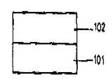
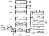
Translated fromKorean제1도는 일반적인 패턴 형성방법.1 is a general pattern forming method.
제2도는 종래의 이층 감광막에 의한 패턴 형성방법.2 is a pattern formation method using a conventional two-layer photosensitive film.
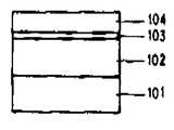
제3도는 종래의 삼층 감광막에 의한 패턴 형성방법.3 is a pattern formation method using a conventional three-layer photosensitive film.
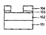
제4도는 본 발명의 이층막 패턴 형성방법.4 is a two-layer film pattern forming method of the present invention.
제5도는 본 발명의 삼층막 패턴 형성방법.5 is a three-layer film pattern forming method of the present invention.
* 도면의 주요부분에 대한 부호의 설명* Explanation of symbols for the main parts of the drawings
101 : 기판 102 : 하층감광막101
103 : 중간 산화막 104 : 상측 감광막103: intermediate oxide film 104: upper photosensitive film
105 : 증착 산화막 106 : 스페이서105: deposited oxide film 106: spacer
107 : SOG107 SOG
본 발명은 반도체 제조공정에 있어서, 미세선폭 가공기술에 관한것으로 특히 반도체소자 제조시 스페이서(Spacer)를 이용한 미세선폭 형성방법에 관한 것이다. 미세선폭 가공기술은 반도체소자 제조시 필요불가결한 기술로서 최근 반도체의 집적도가 증가함에 따라 설계규칙이 점점 줄어들고 있지만 자외선 광원(436nm)을 사용하고 기존의 공정을 사용할 경우 최소선폭은 0.8μm까지만 가능하다. 즉, 제1도에 도시한 종래의 패턴형성방법은 기판(101)위에 상측감광막(104)을 도포한 (a)도와 이를 사진 식각방법으로 노광시킨 (b)도 및 상기 노광후 현상을 한 (c)도와 같은 공정으로 다층감광막을 이용한 미세선폭패턴을 형성하였고, 제2도에 도시한 종래의 이층감광막에 의한 패턴 형성방법은 기판(101)위에 하층감광막(102)을 도포한 (a)도와, 상기 하층감광막(102)위에 상측 감광막(104)을 도포 및 노광시킨 (b)도와, 상기 상측막(104)은 현상하고 상기 하층막(102)은 노광시킨 (c)도 및 상기 하층막(102)을 현상한 (d)도와 같은 공정으로 패턴을 형성하였으며, 제3도에 도시한 종래의 삼층 감광막에 의한 패턴형성방법은 기판(101)위에 하층감광막(102)을 도포한 (a)도와, 상기 하층감광막(102)위에 중간산화막(103)을 증착하고 상측감광막(104)을 도포한 (b)도와 상기 중간 산화막(103)위에 있는 상측감광막(104)을 식각한 (c)도와, 상기 하층감광막(102)위에 있는 중간 산화막(103)을 식각한 (d)도 및 상기 하층감광막(102)을 현상한 (e)도와 같은 공정으로 패턴을 형성하였지만 상기 제1도에서 스텝(step)진 부위에서 선폭변화가 심한 문제점과, 제2도는 제3도의 방법보다는 간단하지만 상측 감광막(104)과 하층감광막(102)사이의 상호혼합(Intermixing)효과가 발생하여 노광후 현상시 많은 문제점이 발생되었다.BACKGROUND OF THE INVENTION 1. Field of the Invention The present invention relates to a fine line width processing technology in a semiconductor manufacturing process, and more particularly, to a method for forming a fine line width using a spacer when manufacturing a semiconductor device. Fine line width processing technology is an indispensable technology in the manufacture of semiconductor devices. As the integration of semiconductors increases recently, design rules are decreasing. However, when using ultraviolet light sources (436 nm) and using conventional processes, the minimum line width is only 0.8 μm. . That is, in the conventional pattern forming method shown in FIG. 1, (a) is coated with the upper
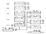
본 발명은 상기와 같은 문제점들을 해결하기 위하여 창안한 것인바, 스페이서(Spacer)형성후 상기 스페이서를 마스크로 한 건식방법으로 행하므로 상호혼합 효과가 발생하지 않도록 하였고 하층감광막을 건식현상할때 중간 산화막층이 마스크 역할을 수행하도록 하였으며 또한 상기 스페이서 만큼의 선폭을 축소하게 되므로 자외선 광원(436nm)을 사용할지라도 0.7μm이하까지 선폭가공을 가능하게 할수 있도록 한 것으로 이하 첨부된 도면에 의하여 본 발명을 상세히 설명하면 다음과 같다. 제4도는 본 발명에 의한 이층막(Bilevel)패턴 형성방법을 도시한 일실시예로서 하층감광막 도포공정(a)은 실리콘기판(101)위에 감광액을 회전 도포기(MTI Spinner)를 사용하여 하층감광막(102)을 rmp 3000에서 두께 1.5μm정도되게 도포한 뒤 컨벡션오븐(Convection oven)에서 200℃이상에서 20분 건조시킨다. 만약 하층에 스텝(Step)이 없을 경우 건식식각기인 드라이(DRIE) 102에서 C2CIF5: 50sccm, 550 Terr, 1min조건으로 플라즈마 처리를 하여 상기 하층감광막(102)을 경화시킨다.The present invention has been devised to solve the above problems, and since the spacer is formed after the formation of the spacer by a dry method using the spacer as a mask so that the intermixing effect does not occur and when the lower layer photoresist is dry, an intermediate oxide film Since the layer serves as a mask and also reduces the line width as much as the spacer, the present invention will be described in detail with reference to the accompanying drawings, which enables line width processing to 0.7 μm or less even when using an ultraviolet light source (436 nm). Is as follows. FIG. 4 is a view illustrating a method of forming a bilevel pattern according to the present invention. In the process of applying a lower layer photoresist film (a), a lower layer photoresist film is formed by using a MTI spinner on a photoresist on a
상기 하층감광막(102)위에 상층감광막(104)을 도포하는 공정 제4b도는 상기 하층감광막(102)위에 다시 회전 도포기를 사용하여 감광액을 rpm 5000-6000에서 두께 4000-5000Å정도 도포한 뒤 연화건조(Soft Bake)를 90˚±3℃에서 5분간 행한다.Step 4b of applying the upper
상기 상층감광막(104) 현상공정(c)은 5X 스테퍼(Stepper)를 사용하여 노광한뒤 D.I Water와 MF-312를 비율 1.5:1로 혼합한 현상액을 습식으로 현상한다. 산화막증착(105) 공정(d)은 실온에서 산화막을 PECVD(Plasma Enhanced Chemical Vapor Deposition)를 사용하여 4000Å정도 증착시킨다.In the developing process (c) of the upper
스페이서(106) 형성공정(e)은 상기 드라이(DRIE)102를 사용하여 C2F6/CHF/He=50/100/50sccm, 550 Terr, 1675W에서 상기 증착산화막(105)을 평면화시켜 스페이서(106)를 형성한다. 즉 스페이서(106) 형성 공정은 그림 1에서와 같이 a와 b의 두께 차이로 a두께만큼 식각 후면 b-a만큼의 스페이서(106)가 남는다.The process of forming the

음성패턴 형성공정 (f)은 상기 드라이(DRIE) 102를 사용하여 O2: 50sccm, 350m Torr, 1675W에서 하층감광막(102)을 건식 현상한다. 즉 제4e-f도에서와 같이 음성패턴을 형성하는 것은 레지스터(102)두께만큼 기언급된 공정조건으로 현상할때 음성패턴 형성공정(f)와 같은 음성패턴이 형성된다. 다음 양성패턴을 형성하기 위한 상층감광막(104) 식각공정(f′)은 상기 상층감광막(104)두께만큼 건식현상을 상기 드라이(DRIE)102를 사용하여 O2: 50sccm, 350m Torr, 1675W 조건에서 행한다. 즉 제4e-f′도는 레지스터(104)두께만큼 현상한 뒤 스페이서(106)를 제거시키면 제거공정(g′)이 된다.In the negative pattern forming process (f), the lower
제거공정(g′)에서 SOG(107)를 도포한 그림이 도포공정(h′)이며 여기서 RIE 식각을 기언급된 SOG(107) 식각 조건으로 오목부분 이외의 두께를 제거하면 평탄화공정(i′)이 된다. 평탄화공정(i′)에서 SOG를 마스크로 레지스터(102)건식 현상하면 양성패턴 형성공정(j′)과 같이 양성패턴이 형성된다. 그리고 (f′)에서 스페이서(106)의 배향(orientation)이 반대인 이유는 제4b-c도의 단계에서 마스크 양성패턴이 반전되기 때문이다.The application of
상기 스페이서(106) 제거공정(g′)은 실온 HF : NH4F=7:1비율로 혼합한 화학약품인 BHF=7:1에서 상기 스페이서(106)를 제거한다. SOG(Spin On Glass)(107) 도포공정(h′)은 상기 회전도포기를 사용하여 상기 SOG(107)를 두께 1μm 102에서 도포하거나 혹은 실리콘이나 금속막을 200℃이하에서 1μm 증착한다.In the
상기 SOG(107) 평탄화공정(i′)은 상기 SOG(107)를 드라이(DRIE)102에서 C2F6/CHF3/He=50/100/50 sccm, 550m Torr, 1675W에서 패턴이 없는 감광막까지 식각한다. 양성패턴 형성공정(j′)은 상기 드라이(DRIE)102를 사용하여 O2: 50sccm, 350Torr,1675W에서 하층감광막(102)을 건식현상한다. 제5도는 본발명에 의한 삼층막(Trilevel)패턴 형성방법을 도시한 일실시예로서 하층감광막(102) 도포공정(a)은 상기 제4도의 하층감광막(102) 도포공정(a)과 같으며 산화막증착 및 상측감광막(104) 도포공정(b)은 산화막을 실온에서 상기 PECVD를 사용하여 1000Å정도 증착시킨 후 나머지 상측감광막(104) 도포는 상기 제4도의 상측감광막 도포공정(b)과 동일 조건으로 행한다.The
상층감광막(104) 현상공정(c)도 상기 제4도의 상층감광막(104) 현상공정과 동일하며 중간층(103) 식각공정 제5d도는 상기 드라이(DRIE) 102에서 C2F6/ CHF3/He=50/100/50sccm, 550m Torr, 1675W에서 식각한다.The developing process (c) of the upper
이하 산화막 증착공정(e) 및 스페이서 형성공정(f), 음성패턴 형성공정(g), 양성패턴을 형성하기 위한 상층감광막(104) 식각공정(g′), 스페이서 제거공정(h′), SOG도포공정(i′), SOG평탄화공정(j′) 양성패턴형성공정(K′)은 각각 제4도의 산화학증착공정(d) 및 스페이서 형성공정(e), 음성패턴 형성공정(f), 양성패턴을 형성하기 위한 상층감광막(104) 식각공정(f′), 스페이서 제거공정(g′), SOG도포공정(h′), SOG평탄화공정(i′), 양성패턴 형성공정(j′)과 동일한 조건으로 행한다.Hereinafter, an oxide film deposition step (e) and a spacer forming step (f), a negative pattern forming step (g), an upper
이상에서 설명한 바와같이 본 발명은 스페이서 형성후 상기 스페이서를 마스크로 한 건식현상방법으로 행하므로 상호 혼합(Intermixing)효과가 발생하지 않는 장점이 있고 또한 제4e-f도나 제4e-f′도로 공정이 진행될 때 공정여유도가 적어 스페이서(106)가 제거되는 경우가 있을 수 있다. 그러나 제5f-g도, 제5f-g′~h′도 공정은 스페이서 자체가 마스크를 하는 경우는 없고 중간산화막(103)과 같이 마스크를 하므로 공정여유도 측면에서 장점이 있는 것이다.As described above, the present invention has the advantage that the intermixing effect does not occur since the spacer is formed by the dry development method using the spacer as a mask, and the process is performed in the 4e-f or 4e-f 'roads. When the process proceeds, there may be a case where the
Claims (4)
Translated fromKoreanPriority Applications (3)
| Application Number | Priority Date | Filing Date | Title |
|---|---|---|---|
| KR1019880009546AKR910010043B1 (en) | 1988-07-28 | 1988-07-28 | Fine Line Width Formation Method Using Spacer |
| JP1073672AJPH0269755A (en) | 1988-07-28 | 1989-03-24 | Fine line width formation method using spacers |
| US07/370,872US5023203A (en) | 1988-07-28 | 1989-06-23 | Method of patterning fine line width semiconductor topology using a spacer |
Applications Claiming Priority (1)
| Application Number | Priority Date | Filing Date | Title |
|---|---|---|---|
| KR1019880009546AKR910010043B1 (en) | 1988-07-28 | 1988-07-28 | Fine Line Width Formation Method Using Spacer |
Publications (2)
| Publication Number | Publication Date |
|---|---|
| KR900002450A KR900002450A (en) | 1990-02-28 |
| KR910010043B1true KR910010043B1 (en) | 1991-12-10 |
Family
ID=19276506
Family Applications (1)
| Application Number | Title | Priority Date | Filing Date |
|---|---|---|---|
| KR1019880009546AExpiredKR910010043B1 (en) | 1988-07-28 | 1988-07-28 | Fine Line Width Formation Method Using Spacer |
Country Status (3)
| Country | Link |
|---|---|
| US (1) | US5023203A (en) |
| JP (1) | JPH0269755A (en) |
| KR (1) | KR910010043B1 (en) |
Families Citing this family (44)
| Publication number | Priority date | Publication date | Assignee | Title |
|---|---|---|---|---|
| GB2297648B (en)* | 1991-08-31 | 1996-10-23 | Samsung Electronics Co Ltd | Semiconductor device |
| TW243541B (en)* | 1991-08-31 | 1995-03-21 | Samsung Electronics Co Ltd | |
| DE4236609A1 (en)* | 1992-10-29 | 1994-05-05 | Siemens Ag | Method for forming a structure in the surface of a substrate - with an auxiliary structure laterally bounding an initial masking structure, followed by selective removal of masking structure using the auxiliary structure as an etching mask |
| KR970000977B1 (en)* | 1993-05-21 | 1997-01-21 | 현대전자산업 주식회사 | Capacitor producing method of semiconductor device |
| KR960011664B1 (en)* | 1993-05-21 | 1996-08-24 | 현대전자산업 주식회사 | Capacitor Formation Method of Semiconductor Device |
| DE69427532T2 (en)* | 1994-02-17 | 2002-04-18 | National Semiconductor Corp., Sunnyvale | METHOD FOR REDUCING THE DISTANCE BETWEEN THE HORIZONTAL NEXT FLOATING GATES OF A FLASH EPROM ARRANGEMENT |
| US5587090A (en)* | 1994-04-04 | 1996-12-24 | Texas Instruments Incorporated | Multiple level mask for patterning of ceramic materials |
| US5523258A (en)* | 1994-04-29 | 1996-06-04 | Cypress Semiconductor Corp. | Method for avoiding lithographic rounding effects for semiconductor fabrication |
| US5494839A (en)* | 1994-05-03 | 1996-02-27 | United Microelectronics Corporation | Dual photo-resist process for fabricating high density DRAM |
| JP3317582B2 (en)* | 1994-06-01 | 2002-08-26 | 菱電セミコンダクタシステムエンジニアリング株式会社 | Method of forming fine pattern |
| KR0154164B1 (en)* | 1994-07-11 | 1998-12-01 | 김주용 | Fabricating method of semiconductor device |
| KR970007173B1 (en)* | 1994-07-14 | 1997-05-03 | 현대전자산업 주식회사 | Fine pattern formation method |
| KR0146246B1 (en)* | 1994-09-26 | 1998-11-02 | 김주용 | Method for manufacturing semiconductor device contact |
| US5628917A (en)* | 1995-02-03 | 1997-05-13 | Cornell Research Foundation, Inc. | Masking process for fabricating ultra-high aspect ratio, wafer-free micro-opto-electromechanical structures |
| US5716859A (en)* | 1995-12-22 | 1998-02-10 | The Whitaker Corporation | Method of fabricating a silicon BJT |
| US5575706A (en)* | 1996-01-11 | 1996-11-19 | Taiwan Semiconductor Manufacturing Company Ltd. | Chemical/mechanical planarization (CMP) apparatus and polish method |
| KR20000004485A (en)* | 1998-06-30 | 2000-01-25 | 김영환 | Method for forming fine patterns of semiconductor devices |
| US6352934B1 (en)* | 1999-08-26 | 2002-03-05 | Infineon Technologies Ag | Sidewall oxide process for improved shallow junction formation in support region |
| US6977203B2 (en) | 2001-11-20 | 2005-12-20 | General Semiconductor, Inc. | Method of forming narrow trenches in semiconductor substrates |
| US7456476B2 (en) | 2003-06-27 | 2008-11-25 | Intel Corporation | Nonplanar semiconductor device with partially or fully wrapped around gate electrode and methods of fabrication |
| US6909151B2 (en)* | 2003-06-27 | 2005-06-21 | Intel Corporation | Nonplanar device with stress incorporation layer and method of fabrication |
| US7154118B2 (en) | 2004-03-31 | 2006-12-26 | Intel Corporation | Bulk non-planar transistor having strained enhanced mobility and methods of fabrication |
| US7579280B2 (en)* | 2004-06-01 | 2009-08-25 | Intel Corporation | Method of patterning a film |
| US7042009B2 (en) | 2004-06-30 | 2006-05-09 | Intel Corporation | High mobility tri-gate devices and methods of fabrication |
| US7348284B2 (en)* | 2004-08-10 | 2008-03-25 | Intel Corporation | Non-planar pMOS structure with a strained channel region and an integrated strained CMOS flow |
| US7422946B2 (en) | 2004-09-29 | 2008-09-09 | Intel Corporation | Independently accessed double-gate and tri-gate transistors in same process flow |
| US7361958B2 (en)* | 2004-09-30 | 2008-04-22 | Intel Corporation | Nonplanar transistors with metal gate electrodes |
| US20060086977A1 (en) | 2004-10-25 | 2006-04-27 | Uday Shah | Nonplanar device with thinned lower body portion and method of fabrication |
| US7518196B2 (en) | 2005-02-23 | 2009-04-14 | Intel Corporation | Field effect transistor with narrow bandgap source and drain regions and method of fabrication |
| US20060202266A1 (en) | 2005-03-14 | 2006-09-14 | Marko Radosavljevic | Field effect transistor with metal source/drain regions |
| US7858481B2 (en) | 2005-06-15 | 2010-12-28 | Intel Corporation | Method for fabricating transistor with thinned channel |
| US7547637B2 (en) | 2005-06-21 | 2009-06-16 | Intel Corporation | Methods for patterning a semiconductor film |
| US7279375B2 (en) | 2005-06-30 | 2007-10-09 | Intel Corporation | Block contact architectures for nanoscale channel transistors |
| US7402875B2 (en) | 2005-08-17 | 2008-07-22 | Intel Corporation | Lateral undercut of metal gate in SOI device |
| US7479421B2 (en) | 2005-09-28 | 2009-01-20 | Intel Corporation | Process for integrating planar and non-planar CMOS transistors on a bulk substrate and article made thereby |
| US20070090416A1 (en) | 2005-09-28 | 2007-04-26 | Doyle Brian S | CMOS devices with a single work function gate electrode and method of fabrication |
| US7485503B2 (en) | 2005-11-30 | 2009-02-03 | Intel Corporation | Dielectric interface for group III-V semiconductor device |
| US20070152266A1 (en)* | 2005-12-29 | 2007-07-05 | Intel Corporation | Method and structure for reducing the external resistance of a three-dimensional transistor through use of epitaxial layers |
| US7407890B2 (en)* | 2006-04-21 | 2008-08-05 | International Business Machines Corporation | Patterning sub-lithographic features with variable widths |
| US8143646B2 (en) | 2006-08-02 | 2012-03-27 | Intel Corporation | Stacking fault and twin blocking barrier for integrating III-V on Si |
| US7772048B2 (en)* | 2007-02-23 | 2010-08-10 | Freescale Semiconductor, Inc. | Forming semiconductor fins using a sacrificial fin |
| ES2489615T3 (en)* | 2007-12-11 | 2014-09-02 | Apoteknos Para La Piel, S.L. | Use of a compound derived from p-hydroxyphenyl propionic acid for the treatment of psoriasis |
| US8362566B2 (en) | 2008-06-23 | 2013-01-29 | Intel Corporation | Stress in trigate devices using complimentary gate fill materials |
| KR101107595B1 (en)* | 2008-12-08 | 2012-01-25 | 한국전자통신연구원 | Transmission line filter structure using double spurline |
Family Cites Families (10)
| Publication number | Priority date | Publication date | Assignee | Title |
|---|---|---|---|---|
| GB1548520A (en)* | 1976-08-27 | 1979-07-18 | Tokyo Shibaura Electric Co | Method of manufacturing a semiconductor device |
| JPS54150970A (en)* | 1978-05-18 | 1979-11-27 | Mitsubishi Electric Corp | Manufacture of semiconductor device |
| JPS5834934B2 (en)* | 1980-06-21 | 1983-07-29 | 工業技術院長 | How to form microstructures |
| JPS5745227A (en)* | 1980-08-29 | 1982-03-15 | Mitsubishi Electric Corp | Manufacture of semiconductor device |
| US4373965A (en)* | 1980-12-22 | 1983-02-15 | Ncr Corporation | Suppression of parasitic sidewall transistors in locos structures |
| JPS57139965A (en)* | 1981-02-24 | 1982-08-30 | Toshiba Corp | Manufacture of semiconductor device |
| US4432132A (en)* | 1981-12-07 | 1984-02-21 | Bell Telephone Laboratories, Incorporated | Formation of sidewall oxide layers by reactive oxygen ion etching to define submicron features |
| US4455742A (en)* | 1982-06-07 | 1984-06-26 | Westinghouse Electric Corp. | Method of making self-aligned memory MNOS-transistor |
| JPS6126221A (en)* | 1984-07-14 | 1986-02-05 | Ricoh Co Ltd | Manufacture of semiconductor device or the like |
| JPS62106456A (en)* | 1985-11-01 | 1987-05-16 | Fujitsu Ltd | Manufacturing method of semiconductor device |
- 1988
- 1988-07-28KRKR1019880009546Apatent/KR910010043B1/ennot_activeExpired
- 1989
- 1989-03-24JPJP1073672Apatent/JPH0269755A/enactiveGranted
- 1989-06-23USUS07/370,872patent/US5023203A/ennot_activeExpired - Fee Related
Also Published As
| Publication number | Publication date |
|---|---|
| JPH0579980B2 (en) | 1993-11-05 |
| US5023203A (en) | 1991-06-11 |
| KR900002450A (en) | 1990-02-28 |
| JPH0269755A (en) | 1990-03-08 |
Similar Documents
| Publication | Publication Date | Title |
|---|---|---|
| KR910010043B1 (en) | Fine Line Width Formation Method Using Spacer | |
| KR0170949B1 (en) | Metal layer formation method | |
| CN1068442C (en) | Method for forming a pattern by silylation | |
| JPH05265186A (en) | Self-aligned phase shift mask and its production | |
| JP2723476B2 (en) | Method for manufacturing phase inversion mask | |
| KR920010129B1 (en) | Pattern forming method of contact hole | |
| JPH058856B2 (en) | ||
| KR0172735B1 (en) | Fabricating method for exposure aligned-key | |
| KR930006133B1 (en) | Contact hole formation method of MOS device | |
| JPH09129604A (en) | Method for forming fine pattern of semiconductor device | |
| JPS61161721A (en) | Surface flattening method | |
| KR100607776B1 (en) | Hardmask Formation Method in Semiconductor Lithography Process | |
| KR101067863B1 (en) | How to form a fine pattern | |
| JPH05283358A (en) | Method of forming contact hole in semiconductor device | |
| KR100559641B1 (en) | Submicron pattern formation method using oxide hard mask | |
| KR0138066B1 (en) | The manufacture of phase shift mask | |
| KR0172522B1 (en) | Resist Pattern Formation Method for Fine Pattern Formation | |
| KR950012541B1 (en) | Method of forming micro pattern of semiconductor device | |
| KR100310942B1 (en) | Photolithography techniques for superconducting device | |
| JP2739793B2 (en) | Manufacturing method of three-phase type phase shift reticle | |
| KR100563819B1 (en) | Method of manufacturing anti-reflection film of semiconductor device | |
| KR100524811B1 (en) | Method for forming fine pattern in semiconductor device | |
| JP2713061B2 (en) | Method of forming resist pattern | |
| KR100928513B1 (en) | Manufacturing method of semiconductor device | |
| KR100268859B1 (en) | Method for forming metal interconnector of semiconductor device |
Legal Events
| Date | Code | Title | Description |
|---|---|---|---|
| A201 | Request for examination | ||
| PA0109 | Patent application | St.27 status event code:A-0-1-A10-A12-nap-PA0109 | |
| PA0201 | Request for examination | St.27 status event code:A-1-2-D10-D11-exm-PA0201 | |
| R17-X000 | Change to representative recorded | St.27 status event code:A-3-3-R10-R17-oth-X000 | |
| PG1501 | Laying open of application | St.27 status event code:A-1-1-Q10-Q12-nap-PG1501 | |
| E902 | Notification of reason for refusal | ||
| PE0902 | Notice of grounds for rejection | St.27 status event code:A-1-2-D10-D21-exm-PE0902 | |
| P11-X000 | Amendment of application requested | St.27 status event code:A-2-2-P10-P11-nap-X000 | |
| P13-X000 | Application amended | St.27 status event code:A-2-2-P10-P13-nap-X000 | |
| G160 | Decision to publish patent application | ||
| PG1605 | Publication of application before grant of patent | St.27 status event code:A-2-2-Q10-Q13-nap-PG1605 | |
| E701 | Decision to grant or registration of patent right | ||
| PE0701 | Decision of registration | St.27 status event code:A-1-2-D10-D22-exm-PE0701 | |
| GRNT | Written decision to grant | ||
| PR0701 | Registration of establishment | St.27 status event code:A-2-4-F10-F11-exm-PR0701 | |
| PR1002 | Payment of registration fee | Fee payment year number:1 St.27 status event code:A-2-2-U10-U11-oth-PR1002 | |
| PR1001 | Payment of annual fee | Fee payment year number:4 St.27 status event code:A-4-4-U10-U11-oth-PR1001 | |
| PR1001 | Payment of annual fee | Fee payment year number:5 St.27 status event code:A-4-4-U10-U11-oth-PR1001 | |
| PR1001 | Payment of annual fee | Fee payment year number:7 St.27 status event code:A-4-4-U10-U11-oth-PR1001 | |
| FPAY | Annual fee payment | Payment date:19980929 Year of fee payment:8 | |
| PR1001 | Payment of annual fee | Fee payment year number:8 St.27 status event code:A-4-4-U10-U11-oth-PR1001 | |
| R18-X000 | Changes to party contact information recorded | St.27 status event code:A-5-5-R10-R18-oth-X000 | |
| LAPS | Lapse due to unpaid annual fee | ||
| PC1903 | Unpaid annual fee | Not in force date:19991211 Payment event data comment text:Termination Category : DEFAULT_OF_REGISTRATION_FEE St.27 status event code:A-4-4-U10-U13-oth-PC1903 | |
| PN2301 | Change of applicant | St.27 status event code:A-5-5-R10-R11-asn-PN2301 St.27 status event code:A-5-5-R10-R13-asn-PN2301 | |
| PC1903 | Unpaid annual fee | Ip right cessation event data comment text:Termination Category : DEFAULT_OF_REGISTRATION_FEE Not in force date:19991211 St.27 status event code:N-4-6-H10-H13-oth-PC1903 | |
| PN2301 | Change of applicant | St.27 status event code:A-5-5-R10-R11-asn-PN2301 St.27 status event code:A-5-5-R10-R13-asn-PN2301 | |
| PN2301 | Change of applicant | St.27 status event code:A-5-5-R10-R11-asn-PN2301 St.27 status event code:A-5-5-R10-R13-asn-PN2301 | |
| PN2301 | Change of applicant | St.27 status event code:A-5-5-R10-R11-asn-PN2301 St.27 status event code:A-5-5-R10-R13-asn-PN2301 | |
| R18-X000 | Changes to party contact information recorded | St.27 status event code:A-5-5-R10-R18-oth-X000 | |
| PN2301 | Change of applicant | St.27 status event code:A-5-5-R10-R11-asn-PN2301 St.27 status event code:A-5-5-R10-R13-asn-PN2301 | |
| PN2301 | Change of applicant | St.27 status event code:A-5-5-R10-R11-asn-PN2301 St.27 status event code:A-5-5-R10-R13-asn-PN2301 | |
| R18-X000 | Changes to party contact information recorded | St.27 status event code:A-5-5-R10-R18-oth-X000 | |
| R18-X000 | Changes to party contact information recorded | St.27 status event code:A-5-5-R10-R18-oth-X000 | |
| R18-X000 | Changes to party contact information recorded | St.27 status event code:A-5-5-R10-R18-oth-X000 | |
| R18-X000 | Changes to party contact information recorded | St.27 status event code:A-5-5-R10-R18-oth-X000 | |
| R18-X000 | Changes to party contact information recorded | St.27 status event code:A-5-5-R10-R18-oth-X000 | |
| PN2301 | Change of applicant | St.27 status event code:A-5-5-R10-R11-asn-PN2301 St.27 status event code:A-5-5-R10-R13-asn-PN2301 | |
| P22-X000 | Classification modified | St.27 status event code:A-4-4-P10-P22-nap-X000 | |
| R18-X000 | Changes to party contact information recorded | St.27 status event code:A-5-5-R10-R18-oth-X000 | |
| R18-X000 | Changes to party contact information recorded | St.27 status event code:A-5-5-R10-R18-oth-X000 |