KR910007384B1 - Formation of superconductor oxide film - Google Patents
Formation of superconductor oxide filmDownload PDFInfo
- Publication number
- KR910007384B1 KR910007384B1KR1019880011900AKR880011900AKR910007384B1KR 910007384 B1KR910007384 B1KR 910007384B1KR 1019880011900 AKR1019880011900 AKR 1019880011900AKR 880011900 AKR880011900 AKR 880011900AKR 910007384 B1KR910007384 B1KR 910007384B1
- Authority
- KR
- South Korea
- Prior art keywords
- superconducting
- magnetic field
- film
- plasma
- superconducting oxide
- Prior art date
- Legal status (The legal status is an assumption and is not a legal conclusion. Google has not performed a legal analysis and makes no representation as to the accuracy of the status listed.)
- Expired
Links
Images

Classifications
- H—ELECTRICITY
- H10—SEMICONDUCTOR DEVICES; ELECTRIC SOLID-STATE DEVICES NOT OTHERWISE PROVIDED FOR
- H10N—ELECTRIC SOLID-STATE DEVICES NOT OTHERWISE PROVIDED FOR
- H10N60/00—Superconducting devices
- H10N60/01—Manufacture or treatment
- H10N60/0268—Manufacture or treatment of devices comprising copper oxide
- H10N60/0296—Processes for depositing or forming copper oxide superconductor layers
- H10N60/0436—Processes for depositing or forming copper oxide superconductor layers by chemical vapour deposition [CVD]
- H10N60/0464—Processes for depositing or forming copper oxide superconductor layers by chemical vapour deposition [CVD] by metalloorganic chemical vapour deposition [MOCVD]
- C—CHEMISTRY; METALLURGY
- C23—COATING METALLIC MATERIAL; COATING MATERIAL WITH METALLIC MATERIAL; CHEMICAL SURFACE TREATMENT; DIFFUSION TREATMENT OF METALLIC MATERIAL; COATING BY VACUUM EVAPORATION, BY SPUTTERING, BY ION IMPLANTATION OR BY CHEMICAL VAPOUR DEPOSITION, IN GENERAL; INHIBITING CORROSION OF METALLIC MATERIAL OR INCRUSTATION IN GENERAL
- C23C—COATING METALLIC MATERIAL; COATING MATERIAL WITH METALLIC MATERIAL; SURFACE TREATMENT OF METALLIC MATERIAL BY DIFFUSION INTO THE SURFACE, BY CHEMICAL CONVERSION OR SUBSTITUTION; COATING BY VACUUM EVAPORATION, BY SPUTTERING, BY ION IMPLANTATION OR BY CHEMICAL VAPOUR DEPOSITION, IN GENERAL
- C23C16/00—Chemical coating by decomposition of gaseous compounds, without leaving reaction products of surface material in the coating, i.e. chemical vapour deposition [CVD] processes
- C23C16/22—Chemical coating by decomposition of gaseous compounds, without leaving reaction products of surface material in the coating, i.e. chemical vapour deposition [CVD] processes characterised by the deposition of inorganic material, other than metallic material
- C23C16/30—Deposition of compounds, mixtures or solid solutions, e.g. borides, carbides, nitrides
- C23C16/40—Oxides
- C23C16/408—Oxides of copper or solid solutions thereof
- C—CHEMISTRY; METALLURGY
- C23—COATING METALLIC MATERIAL; COATING MATERIAL WITH METALLIC MATERIAL; CHEMICAL SURFACE TREATMENT; DIFFUSION TREATMENT OF METALLIC MATERIAL; COATING BY VACUUM EVAPORATION, BY SPUTTERING, BY ION IMPLANTATION OR BY CHEMICAL VAPOUR DEPOSITION, IN GENERAL; INHIBITING CORROSION OF METALLIC MATERIAL OR INCRUSTATION IN GENERAL
- C23C—COATING METALLIC MATERIAL; COATING MATERIAL WITH METALLIC MATERIAL; SURFACE TREATMENT OF METALLIC MATERIAL BY DIFFUSION INTO THE SURFACE, BY CHEMICAL CONVERSION OR SUBSTITUTION; COATING BY VACUUM EVAPORATION, BY SPUTTERING, BY ION IMPLANTATION OR BY CHEMICAL VAPOUR DEPOSITION, IN GENERAL
- C23C16/00—Chemical coating by decomposition of gaseous compounds, without leaving reaction products of surface material in the coating, i.e. chemical vapour deposition [CVD] processes
- C23C16/44—Chemical coating by decomposition of gaseous compounds, without leaving reaction products of surface material in the coating, i.e. chemical vapour deposition [CVD] processes characterised by the method of coating
- C23C16/50—Chemical coating by decomposition of gaseous compounds, without leaving reaction products of surface material in the coating, i.e. chemical vapour deposition [CVD] processes characterised by the method of coating using electric discharges
- C23C16/511—Chemical coating by decomposition of gaseous compounds, without leaving reaction products of surface material in the coating, i.e. chemical vapour deposition [CVD] processes characterised by the method of coating using electric discharges using microwave discharges
- H—ELECTRICITY
- H10—SEMICONDUCTOR DEVICES; ELECTRIC SOLID-STATE DEVICES NOT OTHERWISE PROVIDED FOR
- H10N—ELECTRIC SOLID-STATE DEVICES NOT OTHERWISE PROVIDED FOR
- H10N60/00—Superconducting devices
- H10N60/01—Manufacture or treatment
- H10N60/0268—Manufacture or treatment of devices comprising copper oxide
- H10N60/0296—Processes for depositing or forming copper oxide superconductor layers
- H10N60/0436—Processes for depositing or forming copper oxide superconductor layers by chemical vapour deposition [CVD]
- H—ELECTRICITY
- H10—SEMICONDUCTOR DEVICES; ELECTRIC SOLID-STATE DEVICES NOT OTHERWISE PROVIDED FOR
- H10N—ELECTRIC SOLID-STATE DEVICES NOT OTHERWISE PROVIDED FOR
- H10N60/00—Superconducting devices
- H10N60/01—Manufacture or treatment
- H10N60/0268—Manufacture or treatment of devices comprising copper oxide
- H10N60/0296—Processes for depositing or forming copper oxide superconductor layers
- H10N60/0576—Processes for depositing or forming copper oxide superconductor layers characterised by the substrate
- H—ELECTRICITY
- H10—SEMICONDUCTOR DEVICES; ELECTRIC SOLID-STATE DEVICES NOT OTHERWISE PROVIDED FOR
- H10N—ELECTRIC SOLID-STATE DEVICES NOT OTHERWISE PROVIDED FOR
- H10N60/00—Superconducting devices
- H10N60/01—Manufacture or treatment
- H10N60/0268—Manufacture or treatment of devices comprising copper oxide
- H10N60/0661—Processes performed after copper oxide formation, e.g. patterning
- H10N60/0716—Passivating
- Y—GENERAL TAGGING OF NEW TECHNOLOGICAL DEVELOPMENTS; GENERAL TAGGING OF CROSS-SECTIONAL TECHNOLOGIES SPANNING OVER SEVERAL SECTIONS OF THE IPC; TECHNICAL SUBJECTS COVERED BY FORMER USPC CROSS-REFERENCE ART COLLECTIONS [XRACs] AND DIGESTS
- Y10—TECHNICAL SUBJECTS COVERED BY FORMER USPC
- Y10S—TECHNICAL SUBJECTS COVERED BY FORMER USPC CROSS-REFERENCE ART COLLECTIONS [XRACs] AND DIGESTS
- Y10S505/00—Superconductor technology: apparatus, material, process
- Y10S505/725—Process of making or treating high tc, above 30 k, superconducting shaped material, article, or device
- Y10S505/727—Process of making or treating high tc, above 30 k, superconducting shaped material, article, or device using magnetic field
- Y—GENERAL TAGGING OF NEW TECHNOLOGICAL DEVELOPMENTS; GENERAL TAGGING OF CROSS-SECTIONAL TECHNOLOGIES SPANNING OVER SEVERAL SECTIONS OF THE IPC; TECHNICAL SUBJECTS COVERED BY FORMER USPC CROSS-REFERENCE ART COLLECTIONS [XRACs] AND DIGESTS
- Y10—TECHNICAL SUBJECTS COVERED BY FORMER USPC
- Y10S—TECHNICAL SUBJECTS COVERED BY FORMER USPC CROSS-REFERENCE ART COLLECTIONS [XRACs] AND DIGESTS
- Y10S505/00—Superconductor technology: apparatus, material, process
- Y10S505/725—Process of making or treating high tc, above 30 k, superconducting shaped material, article, or device
- Y10S505/734—From organometallic precursors, e.g. acetylacetonates
- Y—GENERAL TAGGING OF NEW TECHNOLOGICAL DEVELOPMENTS; GENERAL TAGGING OF CROSS-SECTIONAL TECHNOLOGIES SPANNING OVER SEVERAL SECTIONS OF THE IPC; TECHNICAL SUBJECTS COVERED BY FORMER USPC CROSS-REFERENCE ART COLLECTIONS [XRACs] AND DIGESTS
- Y10—TECHNICAL SUBJECTS COVERED BY FORMER USPC
- Y10S—TECHNICAL SUBJECTS COVERED BY FORMER USPC CROSS-REFERENCE ART COLLECTIONS [XRACs] AND DIGESTS
- Y10S505/00—Superconductor technology: apparatus, material, process
- Y10S505/725—Process of making or treating high tc, above 30 k, superconducting shaped material, article, or device
- Y10S505/737—From inorganic salt precursors, e.g. nitrates
Landscapes
- Chemical & Material Sciences (AREA)
- Engineering & Computer Science (AREA)
- Manufacturing & Machinery (AREA)
- Materials Engineering (AREA)
- General Chemical & Material Sciences (AREA)
- Chemical Kinetics & Catalysis (AREA)
- Mechanical Engineering (AREA)
- Metallurgy (AREA)
- Organic Chemistry (AREA)
- Physics & Mathematics (AREA)
- Plasma & Fusion (AREA)
- Inorganic Chemistry (AREA)
- Superconductor Devices And Manufacturing Methods Thereof (AREA)
- Superconductors And Manufacturing Methods Therefor (AREA)
- Inorganic Compounds Of Heavy Metals (AREA)
Abstract
Translated fromKoreanDescription
Translated fromKorean제 1도는 본 발명에서 사용하는 초전도 산호물의 결정구조의 일례를 보이는 사시도.1 is a perspective view showing an example of the crystal structure of the superconducting corals used in the present invention.
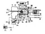
제 2도는 본 발명에서 사용되는 자기 인가 마이크로 웨이브 플라즈마 반응장치를 보이는 도시도.2 is a view showing a magnetically applied microwave plasma reactor used in the present invention.
* 도면의 주요부분에 대한 부호의 설명* Explanation of symbols for main parts of the drawings
10 : 기판 10' : 기판 호울더10: substrate 10 ': substrate holder
11 : 게이트 밸브 14 : 마이크로 웨이브 발진기11: gate valve 14: microwave oscillator
15 : 원통형 자석 16, 17 : 가스 시스템15:
19 : 압력 조절 밸브 24 : 회전 펌프19: pressure regulating valve 24: rotary pump
26 : 진공 펌프 27, 27', 28, 28' :수냉 시스템26:
31 : 플라즈마 발생 챔버 33 : 버블러31: plasma generating chamber 33: bubbler
35 : 동력원 39 : 마이크로 웨이브 유입 윈도우35 power source 39 microwave inflow window
본 발명은 초전도 산화물 세라믹 물질 및 상기 초전도 산화물 제조방법에 관한 것이다.The present invention relates to a superconducting oxide ceramic material and a method for producing the superconducting oxide.
최근 들어 초전도 세라믹 물질이 상당한 관심을 끌고 있다. 상기 물질은 Ba-La-Cu-O(BALACUO)타입 고온 초전도 산화물 형태로 IBM의 쥬리히 연구소에서 먼저 보고되었다. 또한 YBCO(YBa2CuO6-8)타입도 역시 알려져 있다.Recently, superconducting ceramic materials have attracted considerable attention. The material was first reported by IBM's Zurich Institute in the form of a Ba-La-Cu-O (BALACUO) type high temperature superconducting oxide. YBCO (YBa2 CuO6-8 ) type is also known.
그런데, 상기 타입들은 여러 가지 타입의 산화물 분말을 혼합하여 구워내서 정재의 형태로만 준비될 수 있기 때문에 90K의 Tc개시온도가 얻어진다 해도 충분히 얇은 필름은 실현 불가능하다. 게다가, 얇은 필름이 그위에 형성되는 표면부는 비-초전도 특성을 가지며 얇은 필름과 똑같은 결정구조를 갖는다는 것은 완전히 알려지지 않았다.However, since the above types can be prepared by mixing and baking various types of oxide powder only in the form of a tablet, a sufficiently thin film cannot be realized even if a Tc start temperature of 90 K is obtained. In addition, it is not entirely known that the surface portion on which the thin film is formed has non-superconducting properties and has the same crystal structure as the thin film.
다결정 산화물 구조를 갖는 상기 초전도 물질의 임계 전류밀도는 작은편이다. 이러한 문제점을 바로 잡기위해, 결정 알갱이의 모든 ab표면은(c표면을 참조, 표면은 c축방향에 직각이다) 공통으로 방향을 잡는다. 게다가, 초전도 물질과 기판의 온도 팽창계수의 차이가 크기 때문에, 초전도 물질이 650℃보다 높은 온도, 특히 900 내지 950℃의 고온에서 만들어질 때, 액체 질소의 온도에서의 냉각은 균열을 유발하여 전기콘덕턴스가 억제되는 결점이 있다. 상기한 이유 때문에, 기판의 타입을 선택하는데 어느 정도 여유가 있도록, 500℃ 또는 더 낮은 온도에서 필름 형성을 하는 것이 강력히 요구된다. 또한 초전도 산화물의 TCO(저항이 0일 때의 온도)가 높아지는 것이 아주 바람직하다. 액체 질소의 온도 (77K) 또는 더 높은 온도에서 활동이 가능한 것이 바람직하며, 90K 또는 더높은 TCO온도가 얇은 필름의 구조에서 유효한 것이 바람직하다.The critical current density of the superconducting material having a polycrystalline oxide structure is small. To correct this problem, all ab surfaces of the crystal grains (see c surface, the surface is perpendicular to the c axis direction) are oriented in common. In addition, since the difference in the coefficient of thermal expansion of the superconducting material and the substrate is large, when the superconducting material is made at a temperature higher than 650 ° C., especially at a high temperature of 900 to 950 ° C., cooling at the temperature of the liquid nitrogen causes cracking and electric The disadvantage is that conductance is suppressed. For the reasons mentioned above, film formation at 500 ° C. or lower is strongly required so that there is some margin in choosing the type of substrate. In addition, it is very desirable that higher (the temperature when the resistance is zero) of the superconducting oxide TCO. It is desirable to be able to act at a temperature of liquid nitrogen (77 K) or higher, and it is desirable that 90 K or higher TCO temperature be effective in the construction of thin films.
상기 목적을 가지고, 본 발명의 발명자는 가열공정중에 자기장을 가함으로서 초전도 물질을 제조하는 방법인 "초전도 물질 제조 방법"이란 제목의 일본국 특허출원 제62-75205호를 1987년 3월 27일 출원하였다. 본 발명은 앞서 언급한 발명을 좀더 발전시킨 것이다.With the above object, the inventor of the present invention filed March 27, 1987 to Japanese Patent Application No. 62-75205 entitled "Superconducting Material Manufacturing Method" which is a method of manufacturing a superconducting material by applying a magnetic field during the heating process. It was. The present invention further develops the aforementioned invention.
본 발명의 목적은, 상기한 종래의 장치들의 결점을 고려하여, 초전도 산화물의 TCO(저항이 0일 때의 온도)가 고온이며, 액체 질소의 온도 또는 더 높은 온도에서 활동이 가능하고, 얇은 필름의 구조로부터 TCO온도가 90K 또는 그 이상이 되는 초전도 산화물을 제공하려는 것이다.An object of the present invention, in consideration of the drawbacks of the aforementioned conventional apparatus, and TCO (temperature at which resistance is zero) of the superconducting oxide is a high temperature, can be active at a temperature or a higher temperature of liquid nitrogen, and thin It is intended to provide a superconducting oxide having a TCO temperature of 90K or higher from the structure of the film.
본 발명의 또한 목적은 액체 질소의 온도에서의 냉각이 균열을 유발하지 않으며 전기 콘덕턴스가 억제되지 않는 초전도 산화물을 제공함에 있다.It is also an object of the present invention to provide a superconducting oxide in which cooling at the temperature of liquid nitrogen does not cause cracking and the electrical conductance is not suppressed.
자기장이 사용되며 동시에 상기 자기장은 얇은 필름이 그위에 형성되는 표면부에 가해지며, 그러므로 필름의 형성중에 결정의 방향이 얻어지는 반응 가스 또는 플라즈마내의 반응 미소입자 사이의 반응에 의하여 준비되는 초전도 산화물의 얇은 필름을 준비함으로서 상기한 목적들이 본 발명에서 성취된다.A magnetic field is used and at the same time the magnetic field is applied to the surface portion where a thin film is formed thereon, so that during the formation of the film a thin layer of superconducting oxide prepared by reaction between the reactant gas or the reactant microparticles in the plasma where the direction of the crystal is obtained The above objects are achieved in the present invention by preparing a film.
본 발명의 상기한 또는 다른 목적, 특징, 이점 등은 하기되는 부수 도면과 함께 채택된 적절한 실시예를 통하여 더욱 분명해질 것이다.The above or other objects, features, advantages, and the like of the present invention will become more apparent through appropriate embodiments adopted in conjunction with the accompanying drawings.
본 발명에 있어서, 초전도 산화물의 얇은 필름은, 자기장이 사용되고, 동시에 상기 자기장은 얇은 필름이 그위에 형성되는 표면부(이제부터 "필름 형성 표면부"로 인용한다)에 가해지며, 그러므로 필름의 형성중에 결정의 방향이 얻어지는 반응 가스 또는 플라즈마내의 반응 미소입자의 반응에 의해 준비된다.In the present invention, a thin film of superconducting oxide is applied to a surface portion (hereafter referred to as "film forming surface portion") in which a magnetic field is used, and at the same time a thin film is formed thereon, thus forming a film. It is prepared by the reaction of the reaction gas or the reaction microparticles in the plasma from which the direction of the crystal is obtained.
본발명에 있어서, 활성(동작) 온도에서 냉각이 지속되어도 열팽창 계수의 차이는 균열이나 그 유사한 것을 유발하지 않는다. 그 이유는 얇은 필름의 형성온도가 200 내지 500℃ 범위로 낮기 때문이다. 상기 온도에서도 지시된 방향으로 균일하게 향한 결정축을 가진 단결정 또는 다결정이 생성된다. 이제 더 높은 임계 전류밀도를 얻기 위해, 마이크로 웨이브 플라즈마에서 아주 능률적으로 생산되는 O, O3등등과 같은 활성산소가 얇은 필름을 제조하기 위한 반응 가스로 사용된다. 또한 표면부에서 스퍼터링(손상)을 피하기 위해서, 플라즈마 CVD방법이 스퍼터링 방법 대신에 필름 형성방법으로 사용되며, 여기서 고주파수 (500MHz 내지 10GHz) 통상적으로 2.5GHz의 주파수를 갖는 마이크로 웨이브가 이용된다. 플라즈마 CVD방법에서 플라즈마가 생성될 때 에너지는 반응 가스 또는 입자에 운동에너지를 주지 않는다. 게다가 제1도에 도시된 것처럼, 초전도 산화물의 얇은 필름이 만들어질 때, 플라즈마 발생에 이용되는 자기장은 수정된 페로브스카이트(perovskeit)구조를 갖는 결정의 a, b 또는 c축에 평행하게 또는 대충 평행하게 사용된다. 동시에, 상기 자기장을 이용하여 결정의 필름 형성 표면부는 균일한 방향으로 위치하며, 자기 축상 성장이 일어난다. 또한 단결정이 성장되는 경우에는, 자기 에피택셜 성장이 일어난다.In the present invention, even if cooling is continued at the active (operating) temperature, the difference in the coefficient of thermal expansion does not cause cracking or the like. This is because the formation temperature of the thin film is low in the range of 200 to 500 ° C. Even at this temperature, single crystals or polycrystals are produced with crystal axes oriented uniformly in the indicated directions. Now, in order to obtain higher critical current densities, free radicals such as O, O3, etc., which are produced very efficiently in microwave plasma, are used as reaction gases to produce thin films. In addition, in order to avoid sputtering (damage) at the surface portion, the plasma CVD method is used as a film forming method instead of the sputtering method, where microwaves having a frequency of high frequency (500 MHz to 10 GHz) and typically 2.5 GHz are used. In the plasma CVD method, when plasma is generated, energy does not give kinetic energy to the reaction gas or particles. In addition, as shown in FIG. 1, when a thin film of superconducting oxide is made, the magnetic field used for plasma generation is parallel or parallel to the a, b or c axis of the crystal with a modified perovskeit structure. It is used roughly in parallel. At the same time, the film-forming surface portion of the crystal is located in a uniform direction by using the magnetic field, and magnetic axial growth occurs. In addition, when a single crystal is grown, magnetic epitaxial growth occurs.
결론적으로 0.1 또는 그 이상을 사용하여 자기장을 가함으로서 얇은 필름을 형성하며 동시에 표면부에 플라즈마를 생성하는 동안에, 저온에서 적절하게는 200 내지 500℃에서 표면부의 방향을 맞추는 것이 실현가능하다. 동시에 반응가스 또는 반응 입자들은 마이크로 웨이브에 의해 만들어진 활성가스 또는 가스 함유활성산소내에서 상호적으로 플라즈마 반응을 하기가 쉬워지며, 필름 형성 표면부 위에 초전도 산화물 반응 생성물은 상호 일치한 결정축을 갖는 필름을 형성한다.In conclusion it is feasible to orient the surface portion at low temperatures, suitably from 200 to 500 ° C., while forming a thin film by applying a magnetic field using 0.1 or more and simultaneously generating a plasma on the surface portion. At the same time, the reaction gas or reaction particles are easily subjected to plasma reaction in the activated gas or gas-containing active oxygen produced by microwave, and the superconducting oxide reaction products on the film-forming surface portion form a film having mutually coinciding crystal axes. Form.
상기 방법에 의해, 예컨대, c표면(표면은 ab축에, 특히 ab표면에 평행하다)의 방향에서 임계 전류 밀도는 1×10A/㎠ 또는 더 큰 값으로 개선된다. (상기 경우에 있어서, ab표면은 기판의 표면에 평행한 방향으로 될 수 있다. )By this method, for example, in the direction of the c surface (surface is parallel to the ab axis, in particular parallel to the ab surface), the critical current density is improved to a value of 1x10 A / cm 2 or larger. (In this case, the ab surface may be in a direction parallel to the surface of the substrate.)
본 발명에서 사용되는 대표적인 초전도 산화물은 주기율표에서 Ⅱa족 및 Ⅲa족 원소 및 구리를 포함하는 산화물이다.Representative superconducting oxides used in the present invention are oxides comprising Group IIa and Group IIIa elements and copper in the periodic table.
본 발명의 초전도 물질은 일반적으로(A1-XBX)YCuZOW의 식으로 표현될 수 있는데, 여기서 x=0.1 내지1,y=2.0 내지 4.0, 되도록이면 2.5내지 3.5, Z=1.0 내지 4.0, 되도록 1.5 내지 3.5, W=4.0 내지 10.0 되도록이면 6 내지 8이다.The superconducting material of the present invention may be generally represented by the formula (A1-X BX )Y CuZ OW , where x = 0.1 to 1, y = 2.0 to 4.0, preferably 2.5 to 3.5, Z = 1.0 to 4.0, preferably 1.5 to 3.5, and W = 4.0 to 10.0, preferably 6 to 8.
대표적인 한예로는 AB2Cu3O6-8의 식으로 표현되는 수정된 페로브스카이트 구조를 갖는 물질이 있다. A는 이트륨족에서 선택된 원소 및 다른 란탄족에서 선택된 원소들중 한 종류 또는 여러 종류의 원소이다. 이트륨족은 Y(이트륨), Gb(가돌리늄), Yb(이테르븀), Eu(유로퓸) Tb(테르븀), Dg(디스프로슘), Ho(홀뮴), Er(에르븀), Tm(툴륨), Lu(투테륨), Sc(스칸듐) 및 다븐 란탄족으로 구성되는 그룹으로 규정된다-물리 및 화학 사전(이와나미 쇼멘,1963년 4월 1일 간행)One representative example is a material having a modified perovskite structure represented by the formula AB2 Cu3 O6-8 . A is one or several kinds of elements selected from yttrium and other lanthanides. Yttrium groups include Y (yttrium), Gb (gadolinium), Yb (ytterbium), Eu (Europium) Tb (terbium), Dg (dysprosium), Ho (holmium), Er (erbium), Tm (thulium), and Lu (tute) ), Sc (Scandium), and the Dan Lantan Group-Physical and Chemical Dictionary (Iwanami Shomen, published April 1, 1963)
B는 Ba(바륨), Sr(스트론튬), Ca(칼슘)중에서 선택되는 한 종류 또는 여러 종류의 원소이다.B is one or several kinds of elements selected from Ba (barium), Sr (strontium) and Ca (calcium).
본 발명에서 설명되는 초전도 산화물은 제1도에 도시된 결정구조를 가지며, 이는 수정된 페로브스카이트 구조이다. 상기 구조는 구리 (2) 및 그 옆에 산소(5)를 포함하는 평면과 다음에 위치한 구리(3) 및 산소 (6)를 포함하는 또 다른 평면, 산소공백(7), 구리(2'), 산소(5')를 갖는다. 상기 구조는 주기율표의 Ⅲa족에서 원소(1), 예컨데 Y, 및 주기율표의 Ⅱa족에서 원소(4), 예컨데 Ba를 갖는다.The superconducting oxide described in the present invention has the crystal structure shown in FIG. 1, which is a modified perovskite structure. The structure comprises a plane comprising copper (2) and oxygen (5) beside it, and another plane comprising copper (3) and oxygen (6) located next, an oxygen blank (7), copper (2 '). , Oxygen (5 '). The structure has element (1) in group IIIa of the periodic table, eg Y, and element 4 in group IIa of the periodic table, eg Ba.
본 발명의 발명자는, 초전도성을 발생하는 메카니즘으로서, 층구조를 갖는 산소(5), (5')와 상기 층의 중심에 위치한 구리(2), (2')의 상호작용에 의하여 쌍을 이루는 전자들(전자쌍)은 표면(ab축에 형성된 표면, 특히 c표면에 평행한 표면)을 전위한다는 것을 제안하였다. 현재까지 BCS 이론에 근거하여 음향양자의 상호작용히 전자쌍 형성의 원인이 되는 것으로 생각되었다.The inventor of the present invention, as a mechanism for generating superconductivity, is paired by the interaction of oxygen (5), (5 ') having a layer structure and copper (2), (2') located at the center of the layer. It has been suggested that electrons (electron pairs) displace the surface (the surface formed on the ab axis, especially the surface parallel to the c surface). To date, it has been thought that the interaction of acoustic quantum causes electron pair formation based on BCS theory.
그런데, 본 발명의 발명자는 상기 얇은 판자모양의 구조사이의 상부 및 하부 산소 공백(7)(도시도의 상부측 또는 하부측에 위치한 또 다른 공백이 원자 시스템에서 존재한다)이 서로간에 또 스크루 자성체인 희토류 원소(1)와 결합할 때 마그논으로 알려진 유사입자가 발생되며, 이 유사입자는 반대 방향으로 회전하는 한쌍의 전자를 형성하는데 매개물로 작용한다는 이론을 가정하였다. 특히, 마그논은 도면의 c축방향으로 파동하며(ab표면에 직각 방향으로 마그논의 파동은 전자쌍에서 가장 잘 반사된다) 상기 마그논은 상호 반대 방향으로 회전하는 전자쌍중 하나의 전자를 끌어들여 다른 전자에 의해 반발된다. 마그논은 완전히 분명한 것이 아니라 내면적으로 움직이며, 전자쌍은 얇은 판자 모양의 구조를 갖는 표면에서 ((2),(5)로부터 만들어진 표면 및 (2'), (5')로부터 만들어진 표면) 각각의 a-b축에 평행한 방향으로 전위한다.The inventors of the present invention, however, have a screw magnetic body between the upper and lower oxygen vacancies 7 (another vacancies located on the upper side or the lower side of the figure are present in the atomic system) between the lamellar structures. When combined with the phosphorus rare earth element (1), it is assumed that similar particles known as magnons are generated, which act as a medium to form a pair of electrons rotating in opposite directions. In particular, the magnon waves in the c-axis direction of the drawing (the wave of the magneton in the direction perpendicular to the surface ab is best reflected in the electron pair) and the magneton attracts electrons from one of the pairs of electrons rotating in opposite directions. Repulsed by the former. Magnons are not entirely clear but move internally, and the electron pairs are separated from each other (surfaces made from (2) and (5) and surfaces made from (2 ') and (5') on surfaces having a thin board-like structure). Displace in the direction parallel to ab axis.
또한, 산소 공백의 파동은 음향 양자의 파동이라고 여겨지며 따라서 음향 양자가 마그논의 매개를 통하여, 간접적으로 전자쌍의 형성을 야기한다고 생각되는 BCS 이론을 보충하는 패턴을 구비하는 것이 가능하다.In addition, the wave of oxygen vacancies is considered to be a wave of acoustic quantum and thus it is possible to have a pattern that complements the BCS theory that the acoustic quantum indirectly causes the formation of electron pairs through the media of magnon.
상기 작용의 원리에 있어서 자기장이 주요 효과를 야기하기 때문에, 필름 형성 기간중 외부소오스로부터의 프라즈마 대기를 통하여 인가되는 자기장 및 전기장 사이에 상호반응이 행해져서 상호 작용을 위한 반응 가스로부터의 또는 미소 반응 입자의 플라즈마를 생산한다. 더욱이 ,플라즈마 발생에 이용되는 자기장이 활용되어 필름 형성 표면부는 유효 영역에서 상기 자기장에 평행으로 또는 직각으로 위치되며, 그것에 의해 모든 결정은 필름 형성 기간중에 지정된 방향으로 균일하게 위치한다.Since the magnetic field in the principle of the action causes the main effect, the interaction between the magnetic field and the electric field applied through the plasma atmosphere from the external source during the film formation period is performed to react from or from the reaction gas for the interaction Produce a plasma of particles. Moreover, the magnetic field used for plasma generation is utilized so that the film forming surface portion is located parallel or perpendicular to the magnetic field in the effective area, whereby all crystals are uniformly positioned in the designated direction during the film forming period.
게다가, 상기 자기장에 직각 방향으로 특히 초전도성을 갖는 동안 전류가 흐르는 ab표면의 방향으로 마이크로 웨이브 전기장을 가함으로서, 상기 방향 설정의 용이성이 촉진될 수 있다. 특히, 전기 및 자기장의 활성적 상호 이용을 통하여, 상기 반응 압력은 일반적으로 알려진 플라즈마 CVD방법 및 ECR(전자 사이클로브론 공명) 방법에서 사용되는 10-3내지 0.1torr의 저압력이 아니라, 가능한 하이브리드 공명 영역에서 플라즈마 발생이 함께하는 1 내지 800torr의 고 플라즈마 밀도의 아주 높은 압력이다. 여기서, 반응 가스, 반응 입자 및 활성 산소를 상호 사용하여 성취하려는 반응을 수행함으로서, 반응 생성물은 자기장을 따라서 c축으로 방향으로 잡는다.Furthermore, by applying a microwave electric field in the direction perpendicular to the magnetic field in the direction perpendicular to the flowing current while having superconductivity, the ease of setting the direction can be facilitated. In particular, through active mutual use of electric and magnetic fields, the reaction pressure is not as low as 10−3 to 0.1 torr used in commonly known plasma CVD methods and ECR (electron cyclotron resonance) methods, but possible hybrid resonances. Very high pressure with high plasma density of 1 to 800 torr with plasma generation in the region. Here, by performing the reaction to be achieved by using the reaction gas, the reaction particles and the active oxygen together, the reaction product is directed in the c axis along the magnetic field.
이러한 이유로, 축의 반응 생성물은 자기장의 방향에 따라 방향이 설정되며 표면부에 저장된다. 따라서, 필름을 손쉽게 만느는 것이 가능하며 기판의 타입에 대한 제한이 완화된다. 또한 가열하는 중에 자기장을 인가하여 다결정의 각각의 결정축이 일치되거나 대체로 일치되는 다결정 필름을 형성 가능한 것이 바람직하다. 저온에서 자기 에피택셜 성장이 일어나는 것이 바람직하며, 특히 방향축이 성장표면과 일치되는 결정방향을 갖는 기판을 사용하여 단결정 박막이 형성되는 것이 바람직하다.For this reason, the reaction product of the axis is oriented according to the direction of the magnetic field and stored in the surface portion. Thus, it is possible to easily make a film and the restriction on the type of substrate is relaxed. It is also preferable that a magnetic field is applied during heating to form a polycrystalline film in which the respective crystal axes of the polycrystals coincide or are generally coincident. It is preferable that magnetic epitaxial growth takes place at low temperature, and in particular, it is preferable that a single crystal thin film is formed using a substrate having a crystal direction whose direction axis coincides with the growth surface.
상기 경우에 있어, 본 발명에서 사용되는 초전도 산화물은 저온에서 단결정 필름으로부터 얻어진다. 게다가, c평면을 따라 임계 전류 밀도는 2 또는 더 높은 차수의 크기로 c평면에 정상적인 것보다 크다. 이러한 이유로, 다결정을 사용할 때, 분산된 결정 방향을 갖는 다결정은 높은 임계 전류 밀도를 얻기 위하여 한 방향으로 위치한 결정축을 갖도록 배열되는 것이 특히 중요하다.In this case, the superconducting oxide used in the present invention is obtained from a single crystal film at low temperature. In addition, the critical current density along the c plane is greater than normal to the c plane with magnitudes of two or higher orders. For this reason, when using polycrystals, it is particularly important that polycrystals with dispersed crystal directions be arranged with crystal axes located in one direction to obtain a high critical current density.
본 발명은 초전도 산화물을 형성하는 박막 형성방법에 관한 것인데, 여기서 초기 물질 원소의 유기 반응 가스, 예비적으로 초기 물질을 구어내어 생성되는 초전도 산화물의 잘게 분할된 미소 입자 또는 초기 물질의 영류의 미소 입자들은 대기 압력하에서 또는 풍부한 활성가스가 존재하는 감소된 대기하에서 플라즈마로 유입 또는 흩뿌려진다.The present invention relates to a method for forming a thin film for forming a superconducting oxide, wherein an organic reaction gas of an initial material element, finely divided microparticles of a superconducting oxide produced by preliminarily baking an initial material, or a microparticle of permanent current of an initial material They are introduced or scattered into the plasma at atmospheric pressure or in a reduced atmosphere with abundant active gas present.
본 발명에 있어서, 필름을 형성한 후 요구되는 같은 반응롱서의 가열 어니일링을 하는 중에, 결정의 많은 부분 또는 전부는, 특히 다결정이론 배열된 결정은, 자기장을, 0.1 테스라(T) 또는 더 큰 값이 적절하며 통상 0.3 내지 5T로 상기 자기장과 같은 방향으로 또는 그것과 근접한 재배열된 방향으로, 인가함으로서 성장도리 수 있음이 발견되었다. 그리고 자기장의 c축 방향에서 결정이 손쉽게 제공됨이 발견되었다.In the present invention, during the heating annealing of the same reaction cooker required after forming the film, many or all of the crystals, in particular the crystals arranged in polycrystalline theory, have a magnetic field of 0.1 Tesla (T) or more. It has been found that large values are suitable and can be grown by application, usually in the same direction as the magnetic field or in a rearranged direction close to it, typically 0.3 to 5T. And it was found that crystals were readily provided in the c-axis direction of the magnetic field.
상기한 방법에 따라 결정 입자는 다결정으로 발전하여 좀더 크게 한다. 이번에는, 인접한 결정이 똑같은 결정축을 공통으로 소유하기 때문에, 결정 경제면에서의 장벽은 제거되려는 경향이 농후해지며, 단결정 구조가 얻어질 수 있다. 이제, 각각의 결정은 ab표면에서 모두 조절될 수 있다(표면은 c축에 직각), 결론적으로, 본 발명의 방법에 의하면, 무작위 결정방향의 경우에 있어서 현재 102A/cm2(77K)에 가지 이르는 임계 전류 밀도는, ab표면에 평행하게 흐르는 전류에서 104내지 102A/cm2(77K에서 측정)까지 증가하여, 밀도에 있어서 단결정과 동일하게 되거나 또는 약 1/5 수준으로 접근할 수 있다. 이제, 넓은 영역의 단결정 구조 박막을 만드는 것이 좀더 쉬어지며, 상기한 바는 초전도 산화물에 대해 이상적이다.According to the method described above, the crystal grains develop into polycrystals and are made larger. This time, since adjacent crystals share the same crystal axis in common, the barrier in the crystal economy is more likely to be removed, and a single crystal structure can be obtained. Now, each crystal can be adjusted at the ab surface (surface is perpendicular to the c-axis), concludingly, according to the method of the present invention, in the case of random crystallization direction, the current 102 A / cm2 (77K) The critical current density leading to increases from 104 to 102 A / cm2 (measured at 77K) at a current flowing parallel to the ab surface, becoming equal to a single crystal in density or approaching about 1/5 level. can do. It is now easier to make a wide area single crystal structure thin film, which is ideal for superconducting oxides.
본 발명에 있어서, 상기한 축 배열을 한 초전도 박막을 준비함에 있어, 자기장은 박막 표면이 그위에 생성되는 표면부에 직각 또는 수평으로 인가되며, 자기장에 직각으로 활성 산소를 발생하기 위한 마이크로 웨이브 전기장을 인가함으로서, 필름이 형성되는 온도는 효과적으로 낮아진다.In the present invention, in preparing the superconducting thin film having the above-described axial arrangement, the magnetic field is applied at right angles or horizontally to the surface portion on which the thin film surface is formed, and a microwave electric field for generating active oxygen at right angles to the magnetic field. By applying, the temperature at which the film is formed is effectively lowered.
또한, 필름 형성 표면부를 구성하는 기판의 결정축이 자기장에 의해 조절된 결정의 배열 방향을 따르도록 하는 것이 효과적이다. 예를 들어, (100)방향을 갖는 MgO(산화 마그네슘), SrTiO3(스트론튬 산화 티타늄), YSZ(니트륨 안정화 지르콘)의 결정 기판이 이용될 수 있으며, 자기장은 필름 형성 표면부에 직각방향으로 인가되어, 여기서 필름 형성 표면부에 평행한 ab표면 형성이 가능하다. 또한, (110)방향을 갖는 상기 결정 기판을 사용하여, 자기장이 필름 형성 표면부에 평행하게 인가될 때, 필름이 형성된 후 가열 및 자기장 어니일링에 의해 필름 형성 표면부에 직각 방향으로 형성되는 ab표면을 얻는 것이 가능하다. 이제 단결정 박막 또는 단결정과 유사한 모양의 다결정을 포함하는 박막을 얻는 것이 실현 가능하다.Moreover, it is effective to make the crystal axis of the board | substrate which comprises a film formation surface part follow the arrangement direction of the crystal adjusted by the magnetic field. For example, crystal substrates of MgO (magnesium oxide), SrTiO3 (strontium oxide) and YSZ (nitrium stabilized zircon) having a (100) direction may be used, and the magnetic field is perpendicular to the film forming surface portion. Is applied, whereby ab surface formation parallel to the film forming surface portion is possible. Further, using the crystal substrate having the (110) direction, when a magnetic field is applied in parallel to the film forming surface portion, ab is formed at right angles to the film forming surface portion by heating and magnetic field annealing after the film is formed. It is possible to get a surface. It is now feasible to obtain a single crystal thin film or a thin film comprising a polycrystal having a shape similar to that of a single crystal.
[제 1실시예][First Embodiment]
이제 제2도를 참고로 하면, 상기 도면은 본 발명에서 사용되는 자기 인가 마이크로 웨이브 플라즈마 CVD장치를 도시한다.Referring now to FIG. 2, the figure illustrates a magnetically applied microwave plasma CVD apparatus used in the present invention.
상기 도면의 장치는 하기된 것을 구비한다. 대기압 또는 감소된 압력에서 유지될 수 있는 플라즈마 발생챔버(31), 예비 공간(12), 자기장을 발생하는 원통형 전자석(15), 전자석(15)을 위한 동력원(35), 마이크로 웨이브 발진기(14), 배기가스 시스템용 진공 펌프(26), 회전펌프(24), 압력조절밸브(19),기판 호울더(10'), 필름 형성을위한 기판(10), 마이크로 웨이브 유입 윈도우(39)다수의 가스 시스템(16)(17), 다수의 수냉 시스템(28)(28'), 기판(10) 및 호울더(10')를 움직이기 위한 봉(29), 봉(29)의 내부를 통하여 필름이 형성될 표면부를 적당한 온도로 냉각하고 유지하기 위한 다수의 수냉 시스템(27)(27'), 기판 호울더 (10')에는, 플라즈마 발생 챔버(31)내에서 플라즈마로부터 과열되는 기관표면을 적절한 온도로 전환하며 기판을 특유한 온도 예컨대 200내지 500℃로 유지하기 위해 완충층(21)(21') 및 냉각층(22)이 제공된다. 냉각층(22)은 모두 강자성체인 철, 니켈 또는 코발트로 형성되며, 시스템(27)(27')의 냉각수가 순환하도록 일부분에 구멍이 나있다. 완충층(21)(21')은 세라믹, 스테인레스 스틸, 유리와 같은 비-자성, 열저항 물질로 구성된다. 강자성체로 구성된 냉각층(22)은 기판의 표면에서 자기장을 강하게 하여, 과열에 의해 상자성으로 감소하는 피하기 위해 완충층(21,21')에 의해 열로부터 차단된다.The apparatus of the figure has the following.
먼저, 박막 형성을 위한 기판(10)은 기판 호울더(10')은 기판 호울더(10')에 설치되며, 상기 시스템은 게이트 밸브(11)를 통하여 플라즈마 발생 챔버(31)에 위치한다. 본 발명의 상기 실시예에 있어서 실리콘 웨이퍼가 기판으로 시용되어 그 상층 표면의 한 부분위에 IC를 위해 형성되는 절연필름을 구비하며, (100)또는 (110)표면을 갖는 MgO, SiTiO3, YSZ타입도 역시 기판으로 사용될 수 있다.First, the
대기압에서 동작할 때, 밸브(19)는 닫히고 밸브(23)는 열린다. 또한, 감소 압력에서 동작할 때, 밸브(19) 및 (25)는 열리고 밸브(23)는 닫히며, 진공펌프(26) 및 회전 펌프(24)가 동작된다.When operating at atmospheric pressure,
반응 가스 또는 미소 입자가 섞여있는 액체(32)는 혼합되어 버블러(33)에 넣어진다. 화학 증기반응법이 사용되는 경우에, 산소(17)는 팁(34)을 통하여 산소와 함께 플라즈마 발생 챔버(31)로 방출되는 액체(32)로 넘쳐흐른다.The liquid 32 in which the reaction gas or the fine particles are mixed is mixed and put into the bubbler 33. When chemical vapor reaction is used,
분무법이 사용되는 경우, 팁(34)은 분무 노즐로 사용될 수 있다. 산소 또는 공기는 압력이 가해질 수 있으며 가스 시스템(16)에서 유입되고 액체(32)를 사용하는 용액은 압력하에서 팁(34)을 통하여 방출된다.If a spray method is used, the tip 34 may be used as a spray nozzle. Oxygen or air may be pressurized and a solution entering the
제조공정에 있어서, 1×10⁻⁴또는 더 낮은 진공이 기계 보존장치(진공) 펌프(26) 및 회전 펌프(24)를 사용하여 전체 시스템에 우선 가해진다. 다음으로 비-생선가스 (이것은 분해 반응후에 그 스스로 고체를 형성하지 않는 산화가스다. ), N2O, NO, N2O, 공기 또는 산소 예컨대, 산소(6)는 2000SCCM 가스 시스템 (16)을 통과하여 30torr로 압력이 가해지는 플라즈마 발생 챔버(31)로 유입된다. 500MHz의 또는 더 큰 외부 마이크로 웨이브, 예컨대 2.45GHz의 주파수를 가진 마이크로 웨이브(30-2)는 0.5 내지 5KW, 예컨대 1.5KW의 강도로 마이크로 웨이브 발진기(14)에서 인가된다. 또한, (28,28')로 도시된 수냉식의 자석(15)을 사용하여 자기장(30-1)이 인가되며, 여기서 전기 전류가 자석(15)을 통해 흘러서 기판(10)의 표면에서 약 1T의 임계값을 얻으며 하이브리드 공명을 하는 고밀도 플라즈마가 플라즈마 발생챔버(31)에서 발생된다. 이때 자기장(30-1)과 전기장(30-2)은 서로 직각으로 있는다. 도면상에서, 자기장(30-1)은 필름이 형성되는 표면부에 직각으로 인가된다. 상기 고밀도 플라즈마를 이용하여 거의 100% 이온화한 활성 산소가 생성될 수 있다.In the manufacturing process, 1 × 10⁻⁴ or lower vacuum is first applied to the entire system using the mechanical preservation (vacuum) pump 26 and the
다음으로, 용액은 상기 반응 시스템에서 초전도 산화물을 형성하는 유기 원소들로 구성는데, 상기 유기 원소는 예컨대, Y(OC2H5)3(트리에톡시 이트륨), Ba(OC2H5)3(트리에톡시 바륨), CuBr3(브롬화구리) 등등과 같은 알킬화 또는 할로겐화 화합물로서, 필림을 형성한후 벤젠 또는 알콜 등등과 같은 유기용액에서 또는 1 : 2 : 3 비율의 Y : Ba : Cu 수용액에서 용해된다. 예를 들어, 상기 혼합 용액을 통해 산소가 넘쳐흘러 상기 용액은 플라즈마를 통과하여 산소와 함께 유입된다.Next, the solution consists of organic elements which form superconducting oxides in the reaction system, for example Y (OC2 H5 )3 (triethoxy yttrium), Ba (OC2 H5 )3 Alkylated or halogenated compounds such as (triethoxy barium), CuBr3 (copper bromide), etc., which form a film and then in an organic solution such as benzene or alcohol or the like, or an aqueous solution of Y: Ba: Cu in a ratio of 1: 2: 3 Dissolve in For example, oxygen flows through the mixed solution, and the solution flows through the plasma and flows in with the oxygen.
덧붙여서, 다른 방법으로서 YBr3, BaBr2, CuBr2또는 Y(NO3)3, Ba(NO3)2, Cu(N03)2등등과 같은 암모니아 -중화염 생성물이 수용액 또는 유기용액에 용해되며, 고 압력하에서 산소 또는 공기가 상기 용액으로 붙어들어오는 분무법을 사용하여 자기장이 인가 되는 반응실로 유입된다. 운성가스로서의 산소의 반응가스에 대한 비율은 3000에서 1의범위에 있다. (본 경우에 100)In addition, ammonia-neutralized salt products such as YBr3 , BaBr2 , CuBr2 or Y (NO3 )3 , Ba (NO3 )2 , Cu (N03 )2, etc. may be dissolved in an aqueous solution or an organic solution. In a high pressure, oxygen or air is introduced into the reaction chamber to which a magnetic field is applied using a spraying method in which the solution is attached. The ratio of oxygen as a gas to the reaction gas is in the range of 3000 to 1. (100 in this case)
또한 다른 방법으로서, 주기율표의 Ⅱa족 및 Ⅲa족 중의 원소와 구리를 함유한 전도성 산화물의 합성물을 미리 준비하여 잘게 가루로 만들어 용액으로 혼합되며, 이 혼합용액은 분무기 또는 버블러 (33)에 의해 분무되고 플라즈마 발생챔버(31)로 방출되어서 자기장 공간에서 산화 반응이 수행되어 완성된다.As another method, a composite of an element of Groups IIa and IIIa of the Periodic Table and a conductive oxide containing copper is prepared in advance, finely pulverized and mixed into a solution, and the mixed solution is sprayed by an atomizer or bubbler 33. Then, it is discharged into the
상기 방법에서 , 마이크로 웨이브 에너지 및 자기장을 상호 이용하여 하이브리드 공명이 얻어질 때, 플라즈마 온도는 1150℃(전도성 산화물의 용융온도 )보다 훨씬 높으며, 3000 내지 10,000℃ 범위로 높아져서, 그런 고 에너지에서 여기되는 반응원자는 충분히 활성화되고 고유한 결정구조로 필름 형성 표면부위에 형성된다. 상기 초전도 산화물의 박막이 기판 호울더(10')위의 기판의 필름-형성 표면부위에 축적될 수 있으며, 상기 기판의 표면부는 냉각층(22)에 의해 저온으로 냉각되어 기판자체의 온도는 200 내지 500℃의 낮은 범위내에 있는다.In this method, when hybrid resonance is obtained by mutually using the microwave energy and the magnetic field, the plasma temperature is much higher than 1150 ° C (melting temperature of the conductive oxide), and is raised in the range of 3000 to 10,000 ° C, thereby being excited at such high energy. The reactant atoms are sufficiently activated and are formed on the film forming surface with a unique crystal structure. The thin film of superconducting oxide may accumulate on the film-forming surface portion of the substrate on the substrate holder 10 ', and the surface portion of the substrate is cooled to a low temperature by the
그러면, 필름이 형성된 후 400℃에서 어니일링을 하여 제1도에 도시된 것처럼, 1㎛ 내지 1mm의 두께를 갖는 사방형 결정의 수정된 페로브스카이트 구조를 갖는 초전도 산화물 박막을 형성하는 것이 가능하다.It is then possible to form a superconducting oxide thin film with a modified perovskite structure of tetragonal crystals having a thickness of 1 μm to 1 mm by annealing at 400 ° C. after the film is formed. .
제2도에서, 고리모양의 자석(15)이 자기장(30-1)을 발생하는데 사용된다.In FIG. 2, an
결론적으로, 플라즈마 발생 챔버(31)내에는 전기 및 자기장이 상호 작용을 하는 영역(875 가우스 t 185 가우스이내)이 있으며 좀더 센 자기장 강도를 갖는 많은 다른 영역들이 있다.In conclusion, there are regions within the
이제, 기판(10)은 최대 자기장을 갖는 영역 (여기서는 자석(15) 둘레로 중심을 둔 단면이다)에 위치한다. 그러므로, 제1도에 도시된 배열상이 경우에서, 자기장(30-1)은 기판의 필름 형성 표면부에 직각으로 인가되며, 전기장(30-2)은 상기 표면에 평행하게 인가 된다. 자석의 강도로부터, 하이브리드 공명 조건을 만족시키는 875 가우스의 영역이 플라즈마 발생 챔버(31)내의 필름 형성 표면과 가스를 유입하는 노즐(34) 사이의 공간에서 생성될 수 있다.Now, the
산화 초전도성 필름을 생성하기 위한 물질은 하이브리드 공명 영역에서 활성화된 분해 반응을 통하여 c축을 따라 자기장의 방향으로 기판이 필름 형성 표면부위에 필름으로 형성된다.The material for producing the oxidative superconducting film is formed of a substrate on the film formation surface in the direction of the magnetic field along the c axis through the decomposition reaction activated in the hybrid resonance region.
이때 만들어진 초전도 산화물 필림의 임계 전류 밀도는 8.8×10⁴A/cm2으로 기판 표면에 평행하게 측정된다.The critical current density of the superconducting oxide film produced at this time is measured in parallel to the substrate surface at 8.8 × 10⁴ A / cm2 .
특히, 제1도에 도시된 결정구조는 필름이 형성되고, 그뒤에 어니일링하는 시간에 충분히 만들어 진다. 또한, x-선 분석의 결과에 의하면 c축은 자기장에 평행한 방향으로, 특히 필름 형성표면부에 직각 방향으로 형성된다는 것을 알 수 있다.In particular, the crystal structure shown in FIG. 1 is sufficiently made at the time that the film is formed and then annealed. The results of the x-ray analysis also show that the c-axis is formed in a direction parallel to the magnetic field, in particular in a direction perpendicular to the film forming surface portion.
[제2실시예]Second Embodiment
성분요소로서 Y0.5Yb0.5BaSrCu3O6-8의 식으로 표현되는 물질이 사용된다. 특히 기판(10)과 호울더 (10')는 도면상 평면에 대해 직각으로 위치하며 (도면상에서 축방향) 기판은 500℃로 유지된다. 상기 방법에 있어, c축은 직각방향으로 초전도 산화물 박막의 ab표면을 가지며 필름 형성 표면부를 따라 만들어 질 수 있다. 다른 조건들은 제1실시예와 사실상 동일하다. 결론적으로, 예컨대 유리, 알루미나 ZrO2등등과 같은 다결정 또는 비결정 구조 기판의 필름 형성 표면부위에 형성되는 초전도 산화물 박막에 대하여 3.6×10⁴A/cm2의 임계 전류 밀도 및 93K 의 TCO가 얻어진다.As the component element, a substance represented by the formula Y0.5 Yb0.5 BaSrCu3 O6-8 is used. In particular, the
[제3실시예]Third Embodiment
제1실시예의 기판이 MgO(100) 또는 SrTiO3(100)의 단결정으로 바꿔진다. 필름 형성표면부위에 필름을 형성하는데 2T의 자기장이 인가되며, 기판 온도는 450℃로 유지된다. 3.5㎛ 두께의 1cm2또는 좀더 큰 단결정 박막이 기판상에 얻어진다. 2.3 ×10⁶A/cm2(77K)임계 전류 밀도 및 97K의 Tco가 얻어진다.The substrate of the first embodiment is replaced with a single crystal of MgO 100 or SrTiO3 (100). A magnetic field of 2T is applied to form a film on the film formation surface, and the substrate temperature is maintained at 450 ° C. 3.5 cm thick 1 cm2 or larger single crystal thin films are obtained on the substrate. A 2.3 × 10⁶ A / cm2 (77K) critical current density and 97 K of Tco are obtained.
[제4실시예]Fourth Embodiment
제2실시예의 기판은 MgO(100) 또는 SrTiO3(100)의 단결정으로 바꿔진다. 2T의 자기장이 필름형성 표면부에 인가되며, 기판온도는 450℃로 유지된다. 약5mm2, 3㎛ 두께의 단결정 박막이 기판상에 얻어진다. ab 표면과 평행한 표면상에서 1.7 ×10⁶A/cm2의 임계 전류 밀도 및 95K의 Tco가 얻어진다.The substrate of the second embodiment is replaced with a single crystal of MgO 100 or SrTiO3 (100). A magnetic field of 2T is applied to the film forming surface portion, and the substrate temperature is maintained at 450 ° C. A single crystal thin film of about 5 mm2 , 3 μm thick is obtained on the substrate. A critical current density of 1.7 x 10⁶ A / cm2 and a Tco of 95K are obtained on a surface parallel to the ab surface.
[제5실시예][Example 5]
이번 실시예에서, 제1실시예에서 만들어진 초전도 산화물을 갖는 기판은 마이크로웨이브 플라즈마의 활성화된 산소 대기에서 300 내지 500℃의 온도를 15시간 동안 가열 어니일링된다. 이때, 자기장(30-1)은 제2도에 도시된 장치에 의해서 미리 준비된 결정 표면에 대응하는 c축 방향으로 인가된다. 또한, 전기장 (30-2)은 자기장과 직각 방향으로 103내지 5×10⁴V/cm2값으로 인가된다. 결론적으로, Tco를 약 100K보다 높게 증가시키는 것이 가능하며, 230 내지 280K가 얻어진다.In this embodiment, the substrate having the superconducting oxide made in the first embodiment is heat annealed at a temperature of 300 to 500 ° C. for 15 hours in an activated oxygen atmosphere of the microwave plasma. At this time, the magnetic field 30-1 is applied in the c-axis direction corresponding to the crystal surface prepared in advance by the apparatus shown in FIG. Further, the electric field 30-2 is applied at a value of 103 to 5 x 10⁴ V / cm2 in the direction perpendicular to the magnetic field. In conclusion, it is possible to increase Tco higher than about 100 K, with 230-280 K being obtained.
본 발명에 있어서, 얻어진 물질은 박막의 형태로 된다. 그런데, 시장에서의 요구에 따라, 3내지 30 두께의 필름 구조, 띠구조, 와이어 구조와 같은 다른 형태도 역시 얻어질 수 있다.In the present invention, the obtained material is in the form of a thin film. By the way, depending on the market demand, other forms such as 3 to 30 thick film structures, strip structures, and wire structures can also be obtained.
앞서 언급된 본 발명의 장치를 사용하여, 결정축에 순응하는 박막 초전도 산화물을 생성하는 것이 가능하며, 상기 초전도 산화물은 액체 질소의 온도 또는 더 높은 온도에서 동작하는데 상기 조건은 현재까지 실현불가능했다. 또한 비결정유리, 실리콘 산화물, 실리콘 질화물 등등과 같은 기판의 표면상에 방향설정이 된 다결정 초전도 산화물 박막을 제조하는 것도 가능하다. 결정 구조의 성장이 기판 결정축과 방향이 일치하는 경우에 있어서, 상기물질은 반도체와 직접적인 산화반응을 수행하지 않고도 반도체 집적회로의 전극부에서 전기적 접촉이 가능한 단자선으로 이용하는 것이 처음으로 가능해지는데, 왜냐하면 방향 설정된 필름이 200 내지 500℃범위의 기판온도에서 얻어질 수 있기 때문이다.Using the apparatus of the present invention mentioned above, it is possible to produce thin film superconducting oxides that conform to the crystal axis, which superconducting oxides operate at or above the temperature of liquid nitrogen, which conditions have not been realized to date. It is also possible to produce polycrystalline superconducting oxide thin films oriented on the surface of substrates such as amorphous glass, silicon oxide, silicon nitride and the like. In the case where the growth of the crystal structure coincides with the substrate crystal axis, it is possible for the first time that the material is used as a terminal line in which electrical contact is possible at the electrode portion of the semiconductor integrated circuit without performing a direct oxidation reaction with the semiconductor. This is because oriented films can be obtained at substrate temperatures in the range of 200 to 500 ° C.
덧붙여서, 상기 방법에 따라 얻어진 화합물질의 다결정 구조를 갖는 얇은 판자모양의 구조를 형성하기 위하여, 다양한 주기율표 Ⅱa족 및 Ⅲa족중의 여러가지 원소들의 혼합물이 얻어질 수 있다. 본 발명에서 설명한 바와 같이 가열하는 중에 자기장을 인가함으로서 더 균일한 분자 배열이 얻어질 수 있으므로, 최종 화합물에서 빈공간을 제거하여 결정 알갱이 경제면에서 장벽의 높이를 줄이는 것이 가능하여 더 높은 Tco및 개시Tc가 달성될 수 있음이 추측된다.In addition, in order to form a thin board-like structure having a compound polycrystalline structure obtained according to the above method, a mixture of various elements in various periodic table IIa and IIIa groups can be obtained. Since a more uniform molecular arrangement can be obtained by applying a magnetic field during heating as described in the present invention, it is possible to reduce the height of the barrier in terms of crystal grain economy by removing voids in the final compound, resulting in higher Tco and initiation. It is assumed that Tc can be achieved.
다음으로, 다른 형태의 실시예들은 참고로 본 발명의 설명하겠다. 상기 실시예들에서는, 또다른 단계가 포함되는데, 특히, 초전도 특성에 손상을 주는 반응가스 또는 반응 미소 입자가 동시에 첨가되며 ,자기장을 사용하여 플라즈마에서 상호 반응이 행해지고, 상기 자기장은 동시에 필름 형성 표면부에 인가되어, 그것에 의해 필름 형성을 하는 동안 결정의 방향설정을 달성한다. 상기 비-초전도 물질이 기판의 상층부위에 제공된다. 상기 비-초전도 물질에 결정축에 순응하는 같은 결정 구조를 갖는 초전도 산화물을 얇게 씌움으로서, 두층이 같은 열팽창 계수를 갖는 2-층구조가 얻어진다. 그러므로, 2-층구조가 기판 사이의 열팽창 계수의 차이 때문에 균열이나 그 유사한 것이 발생하지 않으며, 활성온도로 물질을 유지하기 위해 냉각이 가해질 때에도, 특유한 결정축의 방향으로 방향 설정된 단결정 또는 다결정이 생성된다. 그러면, 비-초전도 물질위에 얇은 층으로 만들어진 초전도 박막에서 높은 임계 전류 밀도를 달성하기 위하여, 상기 박막을 제조함에 있어서 아주 고 효율로 마이크로웨이브 플라즈마를 가지고 만들어진 O, O3등등과 같은 반응 산소가 반응 가스로서 사용된다. 필름 형성 표면부위에 스퍼터링을 할 때 초전도 산화물 및 필름 형성 표면부의 물질에서 혼합된 위상이 발생하는 것을 방지하기 위하여, 스퍼터링 방법 또는 1KHz 내지 1MHz의 저주파수 플라즈마 CVD방법은 사용되지 않는다. 대신에 고주파수 (500MHz 내지 10GHz) 마이크로웨이브, 통상적으로 2.45GHz가 사용되며, 플라즈마가 형성될 때 에너지는 반응 가스 또는 입자에 운동 에너지로서 주어지지 않는다. 초전도 산화물의 박막이 생성될 때 플라즈마를 발생시키는 자기장이 동시에 사용되어서, 제1도에 도시된 것과 같은 수정된 페로브스카이트 구조를 갖는 결정의 a, b, c 축은 인가된 것에 순응하는 원하는 방향에 대해 평행하게 또는 대체로 평행하게 된다.Next, other forms of embodiments will be described with reference to the present invention. In the above embodiments, another step is included, in particular reaction gases or reaction microparticles damaging the superconducting properties are added at the same time, the mutual reaction is carried out in a plasma using a magnetic field, and the magnetic field simultaneously forms a film forming surface Applied to the portion, thereby achieving crystal orientation during film formation. The non-superconducting material is provided on top of the substrate. By thinly superimposing the non-superconducting material on the superconducting oxide having the same crystal structure conforming to the crystal axis, a two-layer structure in which the two layers have the same coefficient of thermal expansion is obtained. Therefore, the two-layer structure does not cause cracks or the like due to the difference in coefficient of thermal expansion between the substrates, and even when cooling is applied to maintain the material at the active temperature, single crystals or polycrystals oriented in the direction of the specific crystal axis are produced. . Then, in order to achieve a high critical current density in a superconducting thin film made of a thin layer on a non-superconducting material, reactive oxygen such as O, O3, etc. made with a microwave plasma with very high efficiency in producing the thin film is reacted. It is used as a gas. In order to prevent the mixed phase from occurring in the superconducting oxide and the material of the film forming surface when sputtering on the film forming surface portion, the sputtering method or the low frequency plasma CVD method of 1 KHz to 1 MHz is not used. Instead high frequency (500 MHz to 10 GHz) microwaves, typically 2.45 GHz, are used, where energy is not given to the reactant gas or particles as kinetic energy when plasma is formed. When a thin film of superconducting oxide is produced, a magnetic field generating plasma is used simultaneously so that the a, b and c axes of the crystal with a modified perovskite structure as shown in FIG. Parallel to or substantially parallel to.
상기 자기장에 의하여, 결정의 성장표면의 균일한 방향으로 위치하며, 자기 에피택셜 성장이 일어난다. 또한, 단결정이 성장하는 경우에도 자기 에픽택셜 성장이 일어난다. 결과적으로, 박막이 형성하는 동안에 필름 형성 동안 플라즈마를 생성하는데 이용되는 0.1T 또는 그 이상의 자기장을 인가함으로서, 필름형성표면부에서 필름의 방향 설정을 하는 것이 가능해진다. 동시에 반응가스 또는 반응 입자들은 마이크로웨이브에 의해 만들어진 활성 산소 또는 가스 함유 활성 산소내에서 플라즈마 반응을 하며, 초전도 산화물 반응 생성물이 필름 형성 표면부위에 상호 일치된 결정축을 갖는 필름을 형성한다. 상기 방법에 의해, 예컨대 c표면(ab축 특히 ab표면에 평행한 표면)의 방향에서 임계 전류 밀도는 1×10⁶A/cm2또는 더 큰 값으로 개선된다. (이번 경우에, ab표면은 기판의 표면과 평행한 방향으로 있을 수 있다. )The magnetic field is located in a uniform direction of the crystal growth surface, and magnetic epitaxial growth occurs. In addition, magnetic epitaxial growth also occurs when single crystals grow. As a result, by applying a magnetic field of 0.1T or more that is used to generate plasma during film formation during thin film formation, it becomes possible to orient the film at the film formation surface portion. At the same time, the reaction gas or reaction particles undergo a plasma reaction in the active oxygen or gas-containing active oxygen produced by the microwave, and the superconducting oxide reaction product forms a film having crystal axes coinciding with each other on the film forming surface. By this method, for example in the direction of the c surface (surface parallel to the ab axis, in particular the ab surface), the critical current density is improved to 1 × 10⁶ A / cm2 or larger. (In this case, the ab surface may be in a direction parallel to the surface of the substrate.)
상기 실시예들에서, 초전도 산화물 및 그 제조방법은 전술한 실시예들과 동일하므로, 자세한 설명은 생략하겠다.In the above embodiments, the superconducting oxide and the method of manufacturing the same are the same as the above embodiments, detailed description thereof will be omitted.
상기 실시예에서 사용되는 첨가물들은 구리(Cu), 희토류 원소, 철(Fe), 니켈(Ni), 코발트(Co), 실리콘(Si), 게르마늄(Ge), 브롬(B), 알루미늄(Al), 갈륨(Ga), 인(P), 티타늄(Ti), 탄타륨(Ta), 마그네슘(Mg)을 포함하는 그룹중에서 선택되며, 1 내지 30원자%의 양이 사용된다. 특별히 바람직한 원소는 알루미늄 또는 마그네슘이다. 필름이 형성될 때 상기 원소들이 2 내지 10원자%로 첨가되면, 비-초전도 특성을 갖는 필름이 얻어진다. 그러면 첨가물이 더해지지 않은 필름, 특히 똑같은 결정구조 및 결정축을 갖는 초전도 필름이 비-초전도 필름의 상부 또는 하부에 얇은층으로 씌워져서 열팽이계수의 차이가 존재치 않으며 따라서 실제 사용상 온도에서 균열이 발생하지 않는다.Additives used in the above examples are copper (Cu), rare earth elements, iron (Fe), nickel (Ni), cobalt (Co), silicon (Si), germanium (Ge), bromine (B), aluminum (Al) , Gallium (Ga), phosphorus (P), titanium (Ti), tantalum (Ta), magnesium (Mg) is selected from the group containing, the amount of 1 to 30 atomic% is used. Particularly preferred elements are aluminum or magnesium. If the elements are added at 2 to 10 atomic percent when the film is formed, a film having non-superconducting properties is obtained. Then, a film without additives, in particular a superconducting film having the same crystal structure and crystal axis, is covered with a thin layer on the top or the bottom of the non-superconducting film so that there is no difference in coefficient of thermal expansion and thus cracks at the actual operating temperature I never do that.
상기 실시예에서, 먼저 기존 실시예와 똑같은 원리를 이용하여 비-초전도 필름이 형성되며, 다음으로 초전도 필름이 형성되어 비-초전도 필름에 얇은 층으로 씌워진다.In this embodiment, first, a non-superconducting film is formed using the same principle as the previous embodiment, and then a superconducting film is formed and covered with a thin layer on the non-superconducting film.
상기 방법에 있어서, 다결정 구조내의 결정 알갱이는 점점 커질 수 있으며, 인접한 결정들이 동일한 결정축을 공통으로 가지기 때문에, 결정 경계면에서의 장벽은 제거되려는 성향을 더욱 많이 가져서 단결정 구조가 얻어질 수 있다. 이제 각각의 결정들은 모두 ab표면(c표면에 직각인표면)에 배열될 수 있다. 결론적으로, 본 발명의 방법에 의하면, 비-초전도물질과 동일한 구조의 초전도 산화물이 어떤 첨가물이 없이도 만들어지며 비-초전도 물질의 필름 위에 형성되어, 랜덤 결정 방향 설정의 경우에 현재까지 102A/cm2(77K)인 임계 전류 밀도는, ab표면에 평행하게 흐르는 전류에서 104내지 106A/cm2(77K에서 측정)까지 증가하며, 단결정과 전기 밀도가 동일하게 되거나 약 1/5 수준으로 접근할 수 있다.In the above method, the grains of crystals in the polycrystalline structure can be made larger, and since adjacent crystals have the same crystal axis in common, the barrier at the crystal interface has more tendency to be removed so that a single crystal structure can be obtained. Each of the crystals can now be arranged on the ab surface (surface perpendicular to the c surface). In conclusion, according to the method of the present invention, a superconducting oxide of the same structure as the non-superconducting material is made without any additives and is formed on the film of the non-superconducting material, up to 102 A / cm2 (77K) of the critical current density is, in parallel to a current flowing in the
본 발명에서, 상기한 결정 배열을 가진 초전도 박막을 생성함에 있어서, 자기장은 필름 형성표면부에 대해 직각 또는 수평 관계로 인가되며, 활성 산소를 발생시키기 위해 자기장과 직각으로 마이크로웨이브 전기장을 인가함으로서, 필름이 형성되는 온도는 효과적으로 낮춰진다.In the present invention, in producing a superconducting thin film having the above-described crystal arrangement, the magnetic field is applied in a perpendicular or horizontal relationship to the film forming surface portion, by applying a microwave electric field perpendicular to the magnetic field to generate active oxygen, The temperature at which the film is formed is effectively lowered.
이제 특유한 실시예에 대해 설명하겠는데 상기 실시예를 실행하는 방법은 기본적으로 제1 내지 제5실시예와 동일하다. 여기에서, 초전도 필름을 형성하기 이전에는 완전히 똑같은 방법이 비-초전도 필름을 생성 하는데에 사용된다(초전도성을 파괴하는 첨가물이 초전도 물질을 형성 하는원소의 유기 용액에 첨가된다는 점이 예외다). 비-초전도 필름의 형성에 관한 설명만을 하겠고 초전도 필름 형성에 관한 설명은 생략하겠다.A specific embodiment will now be described, but the method of implementing the embodiment is basically the same as the first to fifth embodiments. Here, before forming the superconducting film, exactly the same method is used to produce the non-superconducting film (except that an additive that destroys the superconductivity is added to the organic solution of the element forming the superconducting material). Only the description regarding the formation of the non-superconducting film will be described, and the description regarding the formation of the superconducting film will be omitted.
[제6실시예]Sixth Embodiment
초전도 특성을 파괴하는 첨가물을 사용하여 비-초전도 필름이 먼저 형성된다는 점을 제외하면, 본 실시예에서 사용되는 방법은 제1실시예에서 사용되는 방법에 따른다. 사용되는 첨가물은 예컨데 Al(C2H5)3, Mg(C2H5)3등등과 같은 반응 가스 및 AlBr3, MgBr2, AlCl3, MgCl3등등과 같은 할로겐화 물질들이었다. 상기 첨가물은 초전도성을 발생하기 위한 용액에 규정된 양으로, 예로서, 10원자%로 첨가된다. 산소는 버블링에 의해 혼합 용액에 첨가되며 상기 용액은 산소와 함께 플라즈마로 유입된다.The method used in this embodiment is in accordance with the method used in the first embodiment, except that a non-superconducting film is first formed using additives that destroy the superconducting properties. Additives used were, for example, reaction gases such as Al (C2 H5 )3 , Mg (C2 H5 )3 and the like and halogenated materials such as AlBr3 , MgBr2 , AlCl3 , MgCl3 and the like. The additive is added to the solution for generating superconductivity in a prescribed amount, for example 10 atomic%. Oxygen is added to the mixed solution by bubbling and the solution enters the plasma with oxygen.
비-초전도 산화물 박막을 제조하기 위한 물질은 하이브리드 공명의 영역에서 활성화된 분해 반응이 행해지며, 필름은 c축 및 자기장에 평행하게 형성된다(자기장과 직각인 방향은 자기장을 받아서 활성화되는 기판(10)의 필름 형성 표면 부위로 나온다).The material for producing the non-superconducting oxide thin film is subjected to activated decomposition reaction in the region of hybrid resonance, and the film is formed parallel to the c-axis and the magnetic field (the direction perpendicular to the magnetic field is subjected to the magnetic field to activate the
이때 형성되는 비-초전도 산화물 필름은 Ⅲa1-xXxⅡa2-yYyCu3O6-8X의 일반식으로 표현되는데, 여기서 X와 Y는 첨가물이며, x=0.01 내지 0.3, y=0.01 내지 0.3 이다. 상기 표현식에서, X=Al, Y=Mg, x=0.02, y=0.03이다. 상기 물질은 3×10⁴Ωcm2의 특유한 저항을 가지며 액체질소 온도에서 전혀 초전도성을 보이지 않는다.X-선 분석의 결과에 의하면 상기필름이 자기장과 동일한 방향으로 c축을 갖는 수정된 페로브스카이트 구조를 갖는 것을 분명히 알 수 있다.The non-superconducting oxide film formed at this time is IIIa1-xXxIIa2-yYyCu3O6-8Represented by the general formula of X, where X and Y are additives, and x = 0.01 to 0.3 and y = 0.01 to 0.3. In the above expression, X = Al, Y = Mg, x = 0.02, y = 0.03. The material is 3 × 10⁴Ωcm2It has a unique resistance of and shows no superconductivity at all in liquid nitrogen temperatures.The results of the X-ray analysis clearly show that the film has a modified perovskite structure with a c-axis in the same direction as the magnetic field.
[제7실시예][Example 7]
일반식 Y0.5Yb0.5-xAlxBaSrCu3O6-8으로 표현되는 물질이 구성요소로 사용되는데, 여기서, x=0.01 내지 0.3이며 예로서 x=0.1일 때 Y0.5Yb0.4Al0.1BaSrCu3O6-8으로 주어진다. 특히, 제2도의 장치에서, 기판(10) 및 기판 호울더(10')는 제2도에 직각으로 위치하며(표면은 도면상에서 오른쪽에서 왼쪽방향으로 향한다). 기판의 온도는 500℃로 유지된다. 상기 방법으로 필름 형성 표면부에 평행한 c축과 직각방향으로 비-초전도 산화물 박막의 ab표면을 형성하는 것이 가능하다. 결론적으로, 수정된 페로브스카이트 구조를 갖는 비-초전도 물질의 박막이 예컨대 유리, 알루미나, ZrO2등등과 같은 다결정 또는 비결정 구조 기판의 필름 형성표면위에서 얻어지며, 10Ωcm의 특유한 저항이 얻어진다.A material represented by the general formula Y0.5 Yb0.5-x Alx BaSrCu3 O6-8 is used as a component, wherex 0.51 to 0.3 and for example x = 0.1, Y0.5 Yb0.4 Al0.1 BaSrCu3Given by O6-8 . In particular, in the apparatus of FIG. 2, the
[제8실시예][Example 8]
제6실시예에서의 기판은 MgO(100)또는 SrTiO3(100)의 단결정으로 바꿔진다. 2T의 자기장이 필름 형성 표면 부위의 필름으로 인가되며 기판의 온도는 450℃로 유지된다. Y0.9Al0.1Ba2Cu3O6-8의 일반식으로 표현되는 비-초전도 산화물의 박막이 기판위에 3㎛두께로 형성된다. 이제 YBa2Cu3O6-8의 일반식으로 표현되는 초전도 산화물의 박막이 비-초전도 필름위에 2㎛두께로 형성된다. 상기 방법으로 기판위에 1cm2또는 더 큰 단결정 박막이 얻어 질 수 있다.The substrate in the sixth embodiment is replaced with a single crystal of MgO 100 or SrTiO3 (100). A magnetic field of 2T is applied to the film at the film forming surface area and the temperature of the substrate is maintained at 450 ° C. A thin film of non-superconducting oxide represented by the general formula of Y0.9 Al0.1 Ba2 Cu3 O6-8 is formed on the substrate with a thickness of 3 μm. A thin film of superconducting oxide, represented by the general formula of YBa2 Cu3 O6-8, is now formed on the non-superconducting film with a thickness of 2 μm. In this way a 1 cm2 or larger single crystal thin film can be obtained on the substrate.
3.3×10⁶A/cm2의 임계 전류밀도 및 99K의 Tco가 얻어진다. 기판의 근저에서 열 뒤틀림이 존재하지 않으므로 상기 물질은 개선된 것임을 추측할 수 있다.A critical current density of 3.3 × 10⁶ A / cm2 and a Tco of 99K are obtained. It can be inferred that the material is improved since there is no thermal distortion at the base of the substrate.
[제9실시예][Example 9]
제6실시예에서의 기판은 MgO(110) 또는 SrTiO3(110)의 단결정으로 바꿔진다. 2T의 자기장이 필름 형성 표면부위의 필름에 인가되며 기판의 온도는 450℃로 유지된다. YBa2Cu3O6-8의 일반식으로 표현되는 약5mm2크기의 단결정 박막이 기판위에 3㎛ 두께로 형성된다. 그 다음에, 일반식 Y1Ba2-xMgxCu3O6-8으로 표현되는 물질이 여기에서 x=0.01 내지 0.3이며 예로서 Y1Ba1.9Mg0.1Cu3O6-8이 비-초전도 산화물의 박막에 대해 보호막으로서 0.2㎛ 두께로 형성된다. 2.2×10⁶A/cm2의 임계 전류 밀도가 ab 표면에 평행한 방향으로 초전도 물질에 대해 얻어지며 97K의 Tco가 달성된다. 또한, 104
본 발명에 의하면 균일하게 방향 설정된 결정축을 가지며, 액체 질소의 온도와 동등한 또는 더 높은 온도에서 사용할 수 있는 비-초전도 산화물의 박막을 구비하는 것이 가능하다. 상기된 바는 이전에는 불가능하였다. 또한 비-초전도 산화물과 같은 결정축 및 같은 구조를 가지며 같은 방법으로 마련되는 초전도 산화물의 박막을 구비하며, 상기 초전도 산화물의 비-초전도 산화물의 위, 아래 또는 양측면에 얇은축으로 만드는 것이 실현 가능하다. 상기한 이유 때문에 온도 변화가 있을 때에도, 상기 초전도 산화물은 그것이 절연물과 맞닿는 주변에서 열팽창 뒤틀림을 받지 않으며 고 신뢰성을 보인다. 유리, 실리콘 산화물, 실리콘 질화물 등등으로 만들어진 비결정 구조의 기판 표면위에 방향 설정된 다결정 산화물 비-초전도 박막을 형성하는 것도 또한 가능하다.According to the invention it is possible to have a thin film of non-superconducting oxide which has a uniformly oriented crystal axis and which can be used at a temperature equal to or higher than that of liquid nitrogen. What has been said above has not been possible before. It is also possible to have a thin film of superconducting oxide having the same crystal axis and the same structure as the non-superconducting oxide and provided in the same manner, and to make a thin axis above, below or both sides of the non-superconducting oxide of the superconducting oxide. Even when there is a temperature change for the reasons mentioned above, the superconducting oxide does not undergo thermal expansion distortion around its contact with the insulator and shows high reliability. It is also possible to form oriented polycrystalline oxide non-superconducting thin films on a substrate surface of an amorphous structure made of glass, silicon oxide, silicon nitride and the like.
본 발명에 따라 사용되는 초전도 세라믹은 (A1-xBx)yCuzOw의 화학량 구조식에 일치하여 준비되는데 여기서는 A주기율표의 Ⅲa족중 하나 또는 다수의 원소로, 예컨대 희토류 원소이며, B는 주기율표의 Ⅱa족중 하나 또는 다수의 원소로, 예컨대, 베릴륨 및 마그네슘을 포함하는 알카리 토류 금속이며, x=0 내지 1; y=2.0 내지 4.0 되도록 2.5 내지 3.5; 1.0 내지 4.0 되도록 1.5 내지 3.5; w=4.0 내지 10.0되도록 6.0 내지 8.0이다. 또한, 본 발명에 따라 사용되는 초전도 세라믹은 (A1-xBx)yCuzOw의 화학량적 구조식에 일치하여 준비되는데 여기서 A는 Bi, Sb, As와 같은 주기율표 Ⅴb족의 하나 또는 다수의 원소이며, B는 주기율표 Ⅱa족중 하나 또는 다수의 원소로서 예컨대 베릴륨 및 마그네슘을 포함하는 알카리 토류 금속이며, x=0.3 내지 1; y = 2.0 내지 4.0 되도록 2.5 내지 3.5; z = 1.0 내지 4.0 되도록 1.5 내지 3.5; w=4.0 내지 10.0되도록 9.0 내지 8.0이다. 상기 일반 구조식의 예로는 BiSrCaCaCu2Ox및 Bi4Sr3Ca3Ca3Cu4Ox가 있다. 구조식 Bi4SryCa3Cu4Ox(y는 1.5근처)에 일치하는 것으로 확인된 개시 Tc및 Tco샘플은40 내지 60K로 측정되며, 이는 그리 높은 값이 아니다. 화학량적 구조식 Bi4Sr4Ca2Cu4Ox및 Bi2Sr3Ca2Cu2Ox에 따르는 샘플에서 상대적으로 높은 임계 온도가 얻어진다. 산소의 비율을 지정하는 숫자는 6 내지 10으로 예컨대 8.1근처에 있다.The superconducting ceramics used in accordance with the invention are prepared in accordance with the stoichiometric structural formula of (A1-x Bx )y Cuz Ow , wherein one or more elements of group IIIa of the A periodic table are, for example, rare earth elements, and B is One or more elements of the Group IIa group of the periodic table, such as alkaline earth metals including beryllium and magnesium, wherein x = 0 to 1; 2.5 to 3.5 such that y = 2.0 to 4.0; 1.5 to 3.5, such as 1.0 to 4.0; 6.0-8.0 so that w = 4.0-10.0. In addition, the superconducting ceramics used according to the present invention are prepared in accordance with the stoichiometric structural formula of (A1-x Bx )y Cuz Ow , where A is one or more of the group Vb of the periodic table such as Bi, Sb, As. And B is an alkaline earth metal comprising, for example, beryllium and magnesium, as one or more elements of Group IIa of the Periodic Table, x = 0.3 to 1; 2.5 to 3.5 such that y = 2.0 to 4.0; 1.5 to 3.5 such that z = 1.0 to 4.0; 9.0 to 8.0 so that w = 4.0 to 10.0. Examples of the general structural formulas include BiSrCaCaCu2 Ox and Bi4 Sr3 Ca3 Ca3 Cu4 Ox . The starting Tc and Tco samples found to conform to the structural formula Bi4 Sry Ca3 Cu4 Ox (y is around 1.5) are measured from 40 to 60K, which is not very high. Relatively high critical temperatures are obtained in samples according to the stoichiometric structures Bi4 Sr4 Ca2 Cu4 Ox and Bi2 Sr3 Ca2 Cu2 Ox . The numbers specifying the proportion of oxygen are 6 to 10, for example around 8.1.
Claims (13)
Translated fromKoreanApplications Claiming Priority (6)
| Application Number | Priority Date | Filing Date | Title |
|---|---|---|---|
| JP62231887AJPS6476903A (en) | 1987-09-16 | 1987-09-16 | Apparatus for producing oxide superconducting material |
| JP62-231884 | 1987-09-16 | ||
| JP62231884AJPH0817253B2 (en) | 1987-09-16 | 1987-09-16 | Method for forming oxide superconducting film |
| JP62-231885 | 1987-09-16 | ||
| JP62-231887 | 1987-09-16 | ||
| JP62231885AJP2660246B2 (en) | 1987-09-16 | 1987-09-16 | Superconducting device |
Publications (2)
| Publication Number | Publication Date |
|---|---|
| KR890005815A KR890005815A (en) | 1989-05-17 |
| KR910007384B1true KR910007384B1 (en) | 1991-09-25 |
Family
ID=27331823
Family Applications (1)
| Application Number | Title | Priority Date | Filing Date |
|---|---|---|---|
| KR1019880011900AExpiredKR910007384B1 (en) | 1987-09-16 | 1988-09-15 | Formation of superconductor oxide film |
Country Status (4)
| Country | Link |
|---|---|
| US (2) | US5162296A (en) |
| EP (1) | EP0308266A3 (en) |
| KR (1) | KR910007384B1 (en) |
| CN (1) | CN1016388B (en) |
Families Citing this family (29)
| Publication number | Priority date | Publication date | Assignee | Title |
|---|---|---|---|---|
| EP0267513B1 (en)* | 1986-11-10 | 1998-08-12 | Semiconductor Energy Laboratory Co., Ltd. | Microwave enhanced CVD method and apparatus |
| US6677001B1 (en)* | 1986-11-10 | 2004-01-13 | Semiconductor Energy Laboratory Co., Ltd. | Microwave enhanced CVD method and apparatus |
| JPH0672306B2 (en) | 1987-04-27 | 1994-09-14 | 株式会社半導体エネルギー研究所 | Plasma processing apparatus and plasma processing method |
| DE69016283T3 (en)* | 1989-06-30 | 1998-04-02 | Sumitomo Electric Industries | Substrate with a superconducting layer. |
| EP0450394A3 (en)* | 1990-03-20 | 1991-10-23 | Fujitsu Limited | Method and apparatus for forming superconductor layer |
| JPH07108765B2 (en)* | 1990-04-13 | 1995-11-22 | 東京工業大学長 | Method for producing oxide superconductor thin film by molecular beam epitaxy |
| KR930011413B1 (en) | 1990-09-25 | 1993-12-06 | 가부시키가이샤 한도오따이 에네루기 겐큐쇼 | Plasma cvd method for using pulsed waveform |
| US5779802A (en)* | 1990-12-10 | 1998-07-14 | Imec V.Z.W. | Thin film deposition chamber with ECR-plasma source |
| US6110531A (en)* | 1991-02-25 | 2000-08-29 | Symetrix Corporation | Method and apparatus for preparing integrated circuit thin films by chemical vapor deposition |
| US5648114A (en)* | 1991-12-13 | 1997-07-15 | Symetrix Corporation | Chemical vapor deposition process for fabricating layered superlattice materials |
| US6432554B1 (en) | 1992-02-10 | 2002-08-13 | Iap Research, Inc. | Apparatus and method for making an electrical component |
| US5689797A (en)* | 1992-02-10 | 1997-11-18 | Iap Research, Inc. | Structure and method for compaction of powder-like materials |
| US5405574A (en)* | 1992-02-10 | 1995-04-11 | Iap Research, Inc. | Method for compaction of powder-like materials |
| US6273963B1 (en) | 1992-02-10 | 2001-08-14 | Iap Research, Inc. | Structure and method for compaction of powder-like materials |
| US5611139A (en)* | 1992-02-10 | 1997-03-18 | Iap Research, Inc. | Structure and method for compaction of powder-like materials |
| JP3008970B2 (en)* | 1993-07-27 | 2000-02-14 | 財団法人国際超電導産業技術研究センター | Oxide crystal film having Y123 type crystal structure |
| KR0139876B1 (en)* | 1993-09-14 | 1998-08-17 | 사토 후미오 | Method of forming a metal oxide film |
| US5458086A (en)* | 1993-10-13 | 1995-10-17 | Superconductor Technologies, Inc. | Apparatus for growing metal oxides using organometallic vapor phase epitaxy |
| US6811887B2 (en) | 1996-07-29 | 2004-11-02 | Iap Research, Inc. | Apparatus and method for making an electrical component |
| US7362015B2 (en)* | 1996-07-29 | 2008-04-22 | Iap Research, Inc. | Apparatus and method for making an electrical component |
| US6436252B1 (en) | 2000-04-07 | 2002-08-20 | Surface Engineered Products Corp. | Method and apparatus for magnetron sputtering |
| JP2002343161A (en)* | 2001-05-10 | 2002-11-29 | Univ Tohoku | Method for producing yttrium-based high-temperature superconducting tape |
| US6868778B2 (en)* | 2001-09-14 | 2005-03-22 | Iap Research, Inc. | System and method for loading a plurality of powder materials in an electromagnetic compaction press |
| US8512798B2 (en)* | 2003-06-05 | 2013-08-20 | Superpower, Inc. | Plasma assisted metalorganic chemical vapor deposition (MOCVD) system |
| CN101509122B (en)* | 2009-04-08 | 2012-01-25 | 青岛科技大学 | Process for producing microwave plasma of cuprous iodide semi-conducting film |
| US8592346B2 (en)* | 2010-08-02 | 2013-11-26 | The Texas A&M University System | Textured powder wires |
| CN102730738B (en)* | 2012-06-12 | 2014-06-04 | 北京航空航天大学 | Preparation method of binary or multi-constituent composite rare earth oxide nanoparticles |
| CN113488354A (en)* | 2021-05-27 | 2021-10-08 | 福达合金材料股份有限公司 | Silver tin oxide electric contact material and preparation method thereof |
| CN115717237B (en)* | 2022-10-25 | 2024-11-08 | 新优势产业集团有限公司 | Plasma CVD apparatus with superconducting magnet |
Family Cites Families (8)
| Publication number | Priority date | Publication date | Assignee | Title |
|---|---|---|---|---|
| JPH0635323B2 (en)* | 1982-06-25 | 1994-05-11 | 株式会社日立製作所 | Surface treatment method |
| US4668365A (en)* | 1984-10-25 | 1987-05-26 | Applied Materials, Inc. | Apparatus and method for magnetron-enhanced plasma-assisted chemical vapor deposition |
| US4760008A (en)* | 1986-01-24 | 1988-07-26 | Semiconductor Energy Laboratory Co., Ltd. | Electrophotographic photosensitive members and methods for manufacturing the same using microwave radiation in magnetic field |
| US4776918A (en)* | 1986-10-20 | 1988-10-11 | Hitachi, Ltd. | Plasma processing apparatus |
| US4975411A (en)* | 1987-05-19 | 1990-12-04 | Fonar Corporation | Superconductors and methods of making same |
| US4963524A (en)* | 1987-09-24 | 1990-10-16 | Semiconductor Energy Laboratory Co., Ltd. | Sputtering device for manufacturing superconducting oxide material and method therefor |
| US4939121A (en)* | 1988-10-20 | 1990-07-03 | General Dynamics Corporation, Electronics Division | Method and apparatus for inducing grain orientation by magnetic and electric field ordering during bulk superconductor synthesis |
| US5032568A (en)* | 1989-09-01 | 1991-07-16 | Regents Of The University Of Minnesota | Deposition of superconducting thick films by spray inductively coupled plasma method |
- 1988
- 1988-09-15KRKR1019880011900Apatent/KR910007384B1/ennot_activeExpired
- 1988-09-16CNCN88107276Apatent/CN1016388B/ennot_activeExpired
- 1988-09-16EPEP88308627Apatent/EP0308266A3/ennot_activeWithdrawn
- 1990
- 1990-06-08USUS07/535,302patent/US5162296A/ennot_activeExpired - Fee Related
- 1992
- 1992-05-13USUS07/882,525patent/US5262396A/ennot_activeExpired - Fee Related
Also Published As
| Publication number | Publication date |
|---|---|
| EP0308266A3 (en) | 1989-08-16 |
| CN1016388B (en) | 1992-04-22 |
| US5162296A (en) | 1992-11-10 |
| EP0308266A2 (en) | 1989-03-22 |
| CN1034285A (en) | 1989-07-26 |
| KR890005815A (en) | 1989-05-17 |
| US5262396A (en) | 1993-11-16 |
Similar Documents
| Publication | Publication Date | Title |
|---|---|---|
| KR910007384B1 (en) | Formation of superconductor oxide film | |
| US4963524A (en) | Sputtering device for manufacturing superconducting oxide material and method therefor | |
| Scheel et al. | Problems in epitaxial growth of high-Tc superconductors | |
| US5258364A (en) | Method of shaping superconducting oxide material | |
| Qiu | High-temperature superconductors | |
| JPH0817253B2 (en) | Method for forming oxide superconducting film | |
| US5179073A (en) | Method of shaping superconducting oxide material | |
| EP0349341A2 (en) | Method of improving and/or producing oxide superconductor | |
| JP2660246B2 (en) | Superconducting device | |
| EP0433294B1 (en) | Method of producing a semiconductor device incorporating a superconductor | |
| JP2713343B2 (en) | Superconducting circuit fabrication method | |
| JPH0556283B2 (en) | ||
| JPH0817254B2 (en) | Method for forming oxide superconducting material | |
| JPH01100022A (en) | Method for producing superconducting thin films | |
| JPH0556282B2 (en) | ||
| JP2603688B2 (en) | Superconducting material reforming method | |
| Kuppusami et al. | Processing and properties of thin films of high critical temperature superconductors | |
| JPH0556281B2 (en) | ||
| JP2683689B2 (en) | Method for producing oxide superconducting thin film | |
| JPH0195575A (en) | Formation of oxide superconducting material | |
| JP2564562B2 (en) | How to make superconducting material | |
| JP2668532B2 (en) | Preparation method of superconducting thin film | |
| KR101456152B1 (en) | Superconductor and method of forming the same | |
| Miyazawa et al. | High‐Tc superconducting thin films | |
| JPH0764678B2 (en) | Method for producing superconducting thin film |
Legal Events
| Date | Code | Title | Description |
|---|---|---|---|
| A201 | Request for examination | ||
| PA0109 | Patent application | St.27 status event code:A-0-1-A10-A12-nap-PA0109 | |
| PA0201 | Request for examination | St.27 status event code:A-1-2-D10-D11-exm-PA0201 | |
| R17-X000 | Change to representative recorded | St.27 status event code:A-3-3-R10-R17-oth-X000 | |
| PG1501 | Laying open of application | St.27 status event code:A-1-1-Q10-Q12-nap-PG1501 | |
| G160 | Decision to publish patent application | ||
| PG1605 | Publication of application before grant of patent | St.27 status event code:A-2-2-Q10-Q13-nap-PG1605 | |
| E701 | Decision to grant or registration of patent right | ||
| PE0701 | Decision of registration | St.27 status event code:A-1-2-D10-D22-exm-PE0701 | |
| GRNT | Written decision to grant | ||
| PR0701 | Registration of establishment | St.27 status event code:A-2-4-F10-F11-exm-PR0701 | |
| PR1002 | Payment of registration fee | St.27 status event code:A-2-2-U10-U11-oth-PR1002 Fee payment year number:1 | |
| PR1001 | Payment of annual fee | St.27 status event code:A-4-4-U10-U11-oth-PR1001 Fee payment year number:4 | |
| PR1001 | Payment of annual fee | St.27 status event code:A-4-4-U10-U11-oth-PR1001 Fee payment year number:5 | |
| FPAY | Annual fee payment | Payment date:19960819 Year of fee payment:6 | |
| PR1001 | Payment of annual fee | St.27 status event code:A-4-4-U10-U11-oth-PR1001 Fee payment year number:6 | |
| LAPS | Lapse due to unpaid annual fee | ||
| PC1903 | Unpaid annual fee | St.27 status event code:A-4-4-U10-U13-oth-PC1903 Not in force date:19970926 Payment event data comment text:Termination Category : DEFAULT_OF_REGISTRATION_FEE | |
| PC1903 | Unpaid annual fee | St.27 status event code:N-4-6-H10-H13-oth-PC1903 Ip right cessation event data comment text:Termination Category : DEFAULT_OF_REGISTRATION_FEE Not in force date:19970926 | |
| PN2301 | Change of applicant | St.27 status event code:A-5-5-R10-R13-asn-PN2301 St.27 status event code:A-5-5-R10-R11-asn-PN2301 | |
| P22-X000 | Classification modified | St.27 status event code:A-4-4-P10-P22-nap-X000 | |
| P22-X000 | Classification modified | St.27 status event code:A-4-4-P10-P22-nap-X000 | |
| P22-X000 | Classification modified | St.27 status event code:A-4-4-P10-P22-nap-X000 |