KR910004265B1 - Semiconductor laser system and manufacture method and light head - Google Patents
Semiconductor laser system and manufacture method and light headDownload PDFInfo
- Publication number
- KR910004265B1 KR910004265B1KR1019880003050AKR880003050AKR910004265B1KR 910004265 B1KR910004265 B1KR 910004265B1KR 1019880003050 AKR1019880003050 AKR 1019880003050AKR 880003050 AKR880003050 AKR 880003050AKR 910004265 B1KR910004265 B1KR 910004265B1
- Authority
- KR
- South Korea
- Prior art keywords
- semiconductor laser
- chip
- chips
- laser
- parallel
- Prior art date
- Legal status (The legal status is an assumption and is not a legal conclusion. Google has not performed a legal analysis and makes no representation as to the accuracy of the status listed.)
- Expired
Links
- 239000004065semiconductorSubstances0.000titleclaimsdescription205
- 238000000034methodMethods0.000titleclaimsdescription30
- 238000004519manufacturing processMethods0.000titledescription5
- 230000003287optical effectEffects0.000claimsdescription138
- 229910000679solderInorganic materials0.000claimsdescription35
- 230000010355oscillationEffects0.000claimsdescription29
- 230000004075alterationEffects0.000claimsdescription12
- 239000000463materialSubstances0.000claimsdescription9
- 238000002844meltingMethods0.000claimsdescription8
- 230000008018meltingEffects0.000claimsdescription8
- 230000010287polarizationEffects0.000claimsdescription8
- 230000005540biological transmissionEffects0.000claimsdescription7
- 239000000758substrateSubstances0.000claimsdescription3
- 230000008878couplingEffects0.000claims2
- 238000010168coupling processMethods0.000claims2
- 238000005859coupling reactionMethods0.000claims2
- 230000005284excitationEffects0.000claims1
- 230000005855radiationEffects0.000claims1
- 239000010410layerSubstances0.000description36
- 230000007246mechanismEffects0.000description19
- 230000008569processEffects0.000description18
- 238000001514detection methodMethods0.000description14
- 238000000926separation methodMethods0.000description12
- 230000008859changeEffects0.000description10
- 238000006073displacement reactionMethods0.000description8
- 238000009413insulationMethods0.000description7
- 201000009310astigmatismDiseases0.000description6
- 238000010586diagramMethods0.000description6
- 239000011521glassSubstances0.000description6
- 238000001465metallisationMethods0.000description6
- 229910000980Aluminium gallium arsenideInorganic materials0.000description5
- 239000000919ceramicSubstances0.000description5
- 238000004891communicationMethods0.000description5
- 238000009429electrical wiringMethods0.000description5
- 229910015363Au—SnInorganic materials0.000description4
- 238000009826distributionMethods0.000description4
- 229910020220Pb—SnInorganic materials0.000description3
- 230000000694effectsEffects0.000description3
- 230000010365information processingEffects0.000description3
- 229910045601alloyInorganic materials0.000description2
- 239000000956alloySubstances0.000description2
- 239000012299nitrogen atmosphereSubstances0.000description2
- 230000002093peripheral effectEffects0.000description2
- 238000007747platingMethods0.000description2
- 238000007639printingMethods0.000description2
- 238000003672processing methodMethods0.000description2
- 230000009467reductionEffects0.000description2
- 230000008929regenerationEffects0.000description2
- 238000011069regeneration methodMethods0.000description2
- 238000007493shaping processMethods0.000description2
- 238000002834transmittanceMethods0.000description2
- 229910000531Co alloyInorganic materials0.000description1
- 229910001374InvarInorganic materials0.000description1
- XUIMIQQOPSSXEZ-UHFFFAOYSA-NSiliconChemical compound[Si]XUIMIQQOPSSXEZ-UHFFFAOYSA-N0.000description1
- 229910001128Sn alloyInorganic materials0.000description1
- 239000012790adhesive layerSubstances0.000description1
- 239000006117anti-reflective coatingSubstances0.000description1
- 230000015572biosynthetic processEffects0.000description1
- 229910017052cobaltInorganic materials0.000description1
- 239000010941cobaltSubstances0.000description1
- GUTLYIVDDKVIGB-UHFFFAOYSA-Ncobalt atomChemical compound[Co]GUTLYIVDDKVIGB-UHFFFAOYSA-N0.000description1
- 230000008602contractionEffects0.000description1
- 239000005357flat glassSubstances0.000description1
- 229910052737goldInorganic materials0.000description1
- 238000003384imaging methodMethods0.000description1
- 239000011810insulating materialSubstances0.000description1
- 239000012212insulatorSubstances0.000description1
- 230000002452interceptive effectEffects0.000description1
- 230000001678irradiating effectEffects0.000description1
- 230000005389magnetismEffects0.000description1
- 230000014759maintenance of locationEffects0.000description1
- 238000010309melting processMethods0.000description1
- 229910052759nickelInorganic materials0.000description1
- 239000005304optical glassSubstances0.000description1
- 230000005693optoelectronicsEffects0.000description1
- 230000003647oxidationEffects0.000description1
- 238000007254oxidation reactionMethods0.000description1
- 230000010363phase shiftEffects0.000description1
- 238000010248power generationMethods0.000description1
- 238000010791quenchingMethods0.000description1
- 230000002441reversible effectEffects0.000description1
- 230000035945sensitivityEffects0.000description1
- 229910052710siliconInorganic materials0.000description1
- 239000010703siliconSubstances0.000description1
- 238000010583slow coolingMethods0.000description1
- 229910052719titaniumInorganic materials0.000description1
Images


Classifications
- H—ELECTRICITY
- H01—ELECTRIC ELEMENTS
- H01S—DEVICES USING THE PROCESS OF LIGHT AMPLIFICATION BY STIMULATED EMISSION OF RADIATION [LASER] TO AMPLIFY OR GENERATE LIGHT; DEVICES USING STIMULATED EMISSION OF ELECTROMAGNETIC RADIATION IN WAVE RANGES OTHER THAN OPTICAL
- H01S5/00—Semiconductor lasers
- H01S5/06—Arrangements for controlling the laser output parameters, e.g. by operating on the active medium
- H—ELECTRICITY
- H01—ELECTRIC ELEMENTS
- H01S—DEVICES USING THE PROCESS OF LIGHT AMPLIFICATION BY STIMULATED EMISSION OF RADIATION [LASER] TO AMPLIFY OR GENERATE LIGHT; DEVICES USING STIMULATED EMISSION OF ELECTROMAGNETIC RADIATION IN WAVE RANGES OTHER THAN OPTICAL
- H01S5/00—Semiconductor lasers
- H01S5/02—Structural details or components not essential to laser action
- H01S5/022—Mountings; Housings
- H01S5/02208—Mountings; Housings characterised by the shape of the housings
- H01S5/02212—Can-type, e.g. TO-CAN housings with emission along or parallel to symmetry axis
- G—PHYSICS
- G11—INFORMATION STORAGE
- G11B—INFORMATION STORAGE BASED ON RELATIVE MOVEMENT BETWEEN RECORD CARRIER AND TRANSDUCER
- G11B7/00—Recording or reproducing by optical means, e.g. recording using a thermal beam of optical radiation by modifying optical properties or the physical structure, reproducing using an optical beam at lower power by sensing optical properties; Record carriers therefor
- G11B7/12—Heads, e.g. forming of the optical beam spot or modulation of the optical beam
- G11B7/125—Optical beam sources therefor, e.g. laser control circuitry specially adapted for optical storage devices; Modulators, e.g. means for controlling the size or intensity of optical spots or optical traces
- G11B7/127—Lasers; Multiple laser arrays
- H—ELECTRICITY
- H01—ELECTRIC ELEMENTS
- H01S—DEVICES USING THE PROCESS OF LIGHT AMPLIFICATION BY STIMULATED EMISSION OF RADIATION [LASER] TO AMPLIFY OR GENERATE LIGHT; DEVICES USING STIMULATED EMISSION OF ELECTROMAGNETIC RADIATION IN WAVE RANGES OTHER THAN OPTICAL
- H01S5/00—Semiconductor lasers
- H01S5/02—Structural details or components not essential to laser action
- H01S5/024—Arrangements for thermal management
- H—ELECTRICITY
- H01—ELECTRIC ELEMENTS
- H01S—DEVICES USING THE PROCESS OF LIGHT AMPLIFICATION BY STIMULATED EMISSION OF RADIATION [LASER] TO AMPLIFY OR GENERATE LIGHT; DEVICES USING STIMULATED EMISSION OF ELECTROMAGNETIC RADIATION IN WAVE RANGES OTHER THAN OPTICAL
- H01S5/00—Semiconductor lasers
- H01S5/40—Arrangement of two or more semiconductor lasers, not provided for in groups H01S5/02 - H01S5/30
- H01S5/4025—Array arrangements, e.g. constituted by discrete laser diodes or laser bar
- H—ELECTRICITY
- H01—ELECTRIC ELEMENTS
- H01S—DEVICES USING THE PROCESS OF LIGHT AMPLIFICATION BY STIMULATED EMISSION OF RADIATION [LASER] TO AMPLIFY OR GENERATE LIGHT; DEVICES USING STIMULATED EMISSION OF ELECTROMAGNETIC RADIATION IN WAVE RANGES OTHER THAN OPTICAL
- H01S5/00—Semiconductor lasers
- H01S5/02—Structural details or components not essential to laser action
- H01S5/022—Mountings; Housings
- H01S5/0225—Out-coupling of light
- H01S5/02253—Out-coupling of light using lenses
Landscapes
- Physics & Mathematics (AREA)
- Optics & Photonics (AREA)
- Condensed Matter Physics & Semiconductors (AREA)
- General Physics & Mathematics (AREA)
- Electromagnetism (AREA)
- Semiconductor Lasers (AREA)
- Optical Head (AREA)
Abstract
Translated fromKoreanDescription
Translated fromKorean제 1a 도는 본 발명에 의한 반도체 레이저 장치의 제 1 의 실시예를 도시하는 평면도.1A is a plan view showing a first embodiment of a semiconductor laser device according to the present invention.
제 1a 도는 제 1a 도의 측면도.1a or side view of FIG. 1a.
제 2a 도는 상기 제 1a 도의 중심부를 확대해서 도시한 평면도.FIG. 2A is an enlarged plan view of the center of FIG. 1A; FIG.
제 2b 도는 제 2a 도의 측면도.2b or a side view of FIG. 2a.
제 3 도는 상기 실시예를 광 디스크 장치에 응용한 예를 도시하는 구성도.3 is a configuration diagram showing an example in which the above embodiment is applied to an optical disk device.
제 4 도는 본 발명의 제 2 실시예를 도시하는 평면도.4 is a plan view showing a second embodiment of the present invention.
제 5 도는 본 발명의 제 3 실시예를 도시하는 측면도.5 is a side view showing a third embodiment of the present invention.
제 6 도는 본 발명의 제 4 실시예를 도시하는 평면도.6 is a plan view showing a fourth embodiment of the present invention.
제 7 도는 본 발명의 제 5 실시예의 일부를 단면으로 도시한 사시도.7 is a perspective view showing a part of a fifth embodiment of the present invention in cross section.
제 8 도는 제 5 실시예의 중심부 확대 평면도.8 is an enlarged plan view of the center of the fifth embodiment.
제 9 도는 제 5 실시예의 조립 장치의 구성도.9 is a configuration diagram of an assembling apparatus of a fifth embodiment.
제 10 도는 본 발명의 다른 실시예를 도시하는 광 자기디스크 장치의 광 헤드 구성도10 is an optical head configuration diagram of an optical magnetic disk device showing another embodiment of the present invention.
제 11 도는 제 10 도에 도시한 측면도.11 is a side view shown in FIG.
제 12 도는 제 10 도에 있어서의 광 헤드에 사용되는 반도체 레이저 장치의 평면도.12 is a plan view of a semiconductor laser device used for the optical head shown in FIG.
제 13 도는 트랙 어긋남의 문제를 설명하는 설명도.13 is an explanatory diagram for explaining the problem of track misalignment.
본 발명은 레이저 빔 사이에 근접한 여러개의 독립한 반도체 레이저 칩으로 되는 반도체 레이저 장치와 그 제조방법 및 그것을 사용한 광 헤드에 관한 것이다.BACKGROUND OF THE
현재, 광 디스크 장치나 레이저 빔 프린터 고속화의 고성능화를 목표로한 연구가 한창 진행되고 있다. 광 디스크 장치에 관해서는 여러개의 광 스포트를 사용해서 기록 직후의 여러 체크 기능이나 기록, 재생, 소거기능 또는 2트랙 동시에 기록, 재생을 행하는 병렬처리 기능을 실현하는 방법이 생각되고 있다(예를들면 일본국 특허공개공보 소화61-196446호 참조). 또, 레이저 빔 프린터에 있어서는 마찬가지로 여러개의 광 스포트를 사용하는 것에 의해 기록 속도를 향상시키는 것이 생각되고 있다. 상기 방법을 실현하는 수단의 하나로서 반도체 레이저 어레이의 이용이 검토되고 있다. 상기 반도체 레이저 어레이를 적재한 종래의 반도체 레이저 장치에는 예를들면, 제47회 응용물리학회 학술강연회 예고집. 27p-T-10, p.159(1986년 발행)에 기재되어 있는 바와같이, 모놀리식형과 하이브리드형이 있다.At present, the research which aims at high performance of optical disk apparatus and laser beam printer high speed is in full swing. Regarding the optical disk device, a method of using a plurality of optical spots to realize various check functions immediately after recording, a recording, reproducing, erasing function, or a parallel processing function of simultaneously recording and reproducing two tracks has been conceived (for example, Japanese Patent Laid-Open No. 61-196446). Similarly, in the laser beam printer, it is conceivable to improve the recording speed by using a plurality of optical spots. The use of a semiconductor laser array is considered as one of means for implementing the said method. For example, the 47th Society for Applied Physics Academic Seminars of the conventional semiconductor laser device loaded with the semiconductor laser array. As described in 27p-T-10, p. 159 (issued in 1986), there are monolithic and hybrid types.
모놀리식형은 1개의 반도체 레이저 칩상에 여러개의 반도체 레이저를 어레이화 한 것으로, 그 발광 스포트 간격은 통상 100μm 정도가 최소 한계이다. 하이브리드형은 여러개의 반도체 레이저 칩을 마운트 평면상에 병렬로 배치한 것으로, 그 발광 스포트 간격의 최소 한계는 150μm 정도이다.In the monolithic type, a plurality of semiconductor lasers are arrayed on one semiconductor laser chip, and the emission spot spacing is usually at a minimum of about 100 m. In the hybrid type, several semiconductor laser chips are arranged in parallel on a mount plane, and the minimum limit of the light emission spot spacing is about 150 µm.
또, 종래의 반도체 레이저 장치에 있어서의 어느것의 형에서도 상기 장치에 포함되는 여러개의 반도체 레이저 칩의 발진파장은 동일하였다.Moreover, the oscillation wavelength of the several semiconductor laser chips contained in the said apparatus was the same in any type in the conventional semiconductor laser apparatus.
광 디스크 장치나 레이저 빔 프린터에 있어서는 조여들어간 여러개의 레이저 광의 집광 스포트 간격은 수μm 내지 수십μm로 취하는 것이 요구된다. 그래서, 광 디스크 장치나 레이저 빔 프린터에 사용되는 조리개 광학계의 상의 배율에도 의하지만, 반도체 레이저 장치의 발광 스포트 간격은 100μm 이하인 것이 바람직하다. 이것은 상기 반도체 레이저 장치에 연결하는 광학 렌즈계의 유효시야가 한정되어 있고, 렌즈를 수차가 없는 가까운 축 영역에서 사용할 필요가 있기 때문이다. 이 요구는 광학 렌즈계를 소형화하려고 하면 더욱 어렵게 된다.In an optical disk apparatus or a laser beam printer, it is required to take the condensing spot spacing of several tightened laser lights from several micrometers to several tens of micrometers. Therefore, although it depends also on the magnification of the image of the aperture optical system used for the optical disk apparatus and the laser beam printer, it is preferable that the light emission spot spacing of the semiconductor laser apparatus is 100 m or less. This is because the effective field of view of the optical lens system connected to the semiconductor laser device is limited, and it is necessary to use the lens in the near axial region where there is no aberration. This demand becomes even more difficult when attempting to miniaturize the optical lens system.
종래의 모놀리식형 반도체 레이저 어레이의 경우는 발광 스포트 간격 즉, 반도체 레이저의 어레이 간격을 100μm 이하로 하면, 레이저끼리 열적 및 전기적으로서로 간섭하여 레이저를 독립으로 변조시키는 것이 곤란하게 된다. 따라서, 레이저 발광 스포트 간격을 100μm 이하로 하는데는 기술적으로 큰 문제가 있다.In the case of the conventional monolithic semiconductor laser array, if the emission spot spacing, that is, the array spacing of the semiconductor lasers is 100 m or less, it is difficult to mutually modulate the lasers independently by interfering with the lasers thermally and electrically. Therefore, there is a technical problem in making the laser emission spot spacing 100 μm or less.
한편, 반도체 레이저를 평면상으로 병렬 배치한 종래의 하이브리드형에서는 레이저 활성층의 가장 가까운 곳에서 레이저 칩을 절단하지 않으면 안되고, 레이저에 왜곡의 열화가 생겨서 레이저 수명이 짧게 된다는 문제가 발생한다. 따라서 발광 스포트 간격은 역시 100μm 이하로 좁게할 수가 없다.On the other hand, in the conventional hybrid type in which semiconductor lasers are arranged in parallel on a plane, the laser chip must be cut at the closest portion of the laser active layer, which causes a problem that the laser life is shortened due to distortion of the laser. Therefore, the emission spot interval cannot be narrowed to 100 μm or less.
그러나, 광 디스크 장치에 있어서 디스크의 회전 기다림없이 리얼 타임에 기록 재생을 행하는데는 라이트 소거용에 고출력, 재생용에 저잡음의 최저 2개의 반도체 레이저가 필요하다. 또, 반도체 레이저의 발진파장이 같으면, 신호 검출계에서 빔을 공간적으로 분리하지 않으면 안되고, 광학계가 복잡하게 되어 소형화, 저렴화의 면에서 불리하다. 그러나, 모놀리식형에서는 파장, 출력 및 잡음 특성이 다른 레이저를 어레이화 하는 것은 반도체 제조 프로세스상 매우 곤란하다.However, in the optical disk apparatus, at least two semiconductor lasers of high power for light erasing and low noise for reproduction are required for recording and reproducing in real time without waiting for the rotation of the disk. In addition, if the oscillation wavelength of the semiconductor laser is the same, the beam must be spatially separated from the signal detection system, and the optical system becomes complicated, which is disadvantageous in terms of miniaturization and cost reduction. However, in the monolithic type, it is very difficult in the semiconductor manufacturing process to array lasers having different wavelengths, outputs and noise characteristics.
한편, 반도체 레이저 장치를 광 헤드로써 사용한 광 디스크 장치의 디스크면 상의 스포트 간격 ℓ은 레이저 다이오드 간격 d와 조준 렌즈의 열림구멍 수 NAc와 포커스 렌즈의 열림구멍 수 NAf로 결정되어On the other hand, the spot spacing ℓ on the disk surface of the optical disk device using the semiconductor laser device as the optical head is determined by the laser diode spacing d, the opening hole number NAc of the aiming lens and the opening hole number NAf of the focus lens.

로 된다. 반도체 레이저에서 출사하는 빔을 유효하게 집결해서 기록이나 소거를 달성하기 위해서는 NAc가 예를들면 0.2 이상의 조준 렌즈가 통상 널리 사용되고 있다. 또, 기록용의 광 헤드에서는 NAf가 예를들면 0.5의 포커스 렌즈가 널리 사용되고 있다. 그래서, 모놀리식형 반도체 레이저 어레이를 사용한 상기 종래예와 같은 광 헤드에서는 d

디스크면 상의 스포트 간격이 40μm이면 광 디스크 장치에 있어서는 트랙 어긋남이 약 0.13μm로 되고 이것은 허용되는 트랙 어긋남을 초월하고 만다.If the spot spacing on the disk surface is 40 µm, the track shift becomes about 0.13 µm in the optical disk apparatus, which exceeds the allowable track shift.
본 발명의 목적은 특성이 다른 반도체 레이저를 여러개 적재하고 또한, 상기 반도체 레이저의 발광 스포트 간격을 100μm 이하로 하는 것이 가능한 반도체 레이저 장치를 얻는 것에 있다.An object of the present invention is to obtain a semiconductor laser device capable of stacking a plurality of semiconductor lasers having different characteristics and setting the emission spot spacing of the semiconductor laser to 100 m or less.
본 발명의 다른 목적은 파장이 다른 여러개의 레이저 빔을 소정위치에 색수차 없이 조사하는 것이 가능한 반도체 레이저 장치를 얻는 것에 있다.Another object of the present invention is to obtain a semiconductor laser device capable of irradiating several laser beams having different wavelengths to a predetermined position without chromatic aberration.
본 발명의 또 다른 목적은 발광 스포트 간격 100μm 이하의 반도체 레이저를 소정의 위치에 배치하는 것이 가능한 반도체 레이저 장치의 제조방법을 제공하는데 있다.It is still another object of the present invention to provide a method of manufacturing a semiconductor laser device capable of disposing a semiconductor laser having a light emission spot interval of 100 m or less at a predetermined position.
본 발명의 목적은 디스크면 상의 2개의 스포트 간격을 40μm 이하, 더 나아가서는 20μm 이하로 할 수가 있는 2빔 광 헤드를 제공하는 것에 있다. 또, 2개의 빔의 분사가 용이하고, 얇은형으로 하는 것이 가능한 2빔 광 헤드를 제공하는 것에 있다.It is an object of the present invention to provide a two-beam optical head capable of setting two spot spacings on a disk surface to 40 µm or less, further 20 µm or less. Another object of the present invention is to provide a two-beam optical head which can easily eject two beams and can be made thin.
상기 목적은 하이브리드형의 반도체 레이저 장치에 있어서, 2개의 반도체 레이저 칩은 공간을 두고 서로 마주대하는 2개의 면에 각각 분리해서 고착하는 내장 구조를 채용하는 것에 의해서 달성된다.The above object is achieved by employing a built-in structure in which two semiconductor laser chips are separately fixed to two surfaces facing each other with a space therebetween.
상기 해결수단에 의하면, 2개의 반도체 레이저의 활성층을 약간의 공간을 두고 근접시키는 것이 가능하게 된다. 즉, 하이브리드형의 반도체 레이저 장치에 의해 2개의 반도체 레이저 칩은 공간을 두고 서로 마주대하는 2개면에 각각 분리해서 고착하는 것에 의해서, 종래의 반도체 레이저 칩에 특별한 가공을 행하지 않아도, 전극과 활성층 간격의 2배 정도까지의 반도체 레이저의 발광 스포트 간격을 좁게 할 수가 있어, 100μm 이하의 간격을 용이하게 실현할 수 있다.According to the above solution, it is possible to bring the active layers of the two semiconductor lasers close to each other with some space. That is, the two semiconductor laser chips are separated and fixed to two surfaces facing each other with a space by a hybrid semiconductor laser device, so that the gap between the electrode and the active layer can be eliminated even without special processing on the conventional semiconductor laser chip. It is possible to narrow the light emission spot interval of the semiconductor laser up to about 2 times, and it is possible to easily realize the interval of 100 μm or less.
또, 하이브리드형이기 때문에 특성이 다른 반도체 레이저를 적재하는 것이 가능하다. 또, 상기 반도체 레이저는 각각 독립 분리한 위치에서 장치에 부착되므로, 레이저끼리의 열적 및 전기적인 간섭이 일어나지 않고, 각각의 레이저를 독립으로 변조시킬 수가 있다.In addition, because of the hybrid type, it is possible to load semiconductor lasers having different characteristics. In addition, since the semiconductor lasers are attached to the devices at positions separated from each other, thermal and electrical interference between the lasers does not occur, and each laser can be independently modulated.
본 발명의 반도체 레이저 장치의 제조방법에 있어서는, 각 반도체 레이저는 각각 개별적으로 위치결정되어서 유지되어 각 반도체 레이저를 기본으로 고정하는 것에 의해 조립된다. 이 경우에 각 반도체 레이저는 각각 지지체에 부착되고, 이 각각의 지지체는 접착제층에 의해 기체에 고정하도록 하는 것이 바람직하다.In the method of manufacturing a semiconductor laser device of the present invention, each semiconductor laser is individually positioned and held, and assembled by fixing each semiconductor laser as a basis. In this case, it is preferable that each semiconductor laser is attached to the support, and each support is fixed to the substrate by an adhesive layer.
본 발명의 광 헤드에 있어서는, 2개의 반도체 레이저 칩을 대향시켜서 배치하고, 2개의 반도체 레이저 칩에서 방사되는 2개의 레이저 빔은 동일한 렌즈계에 의해서 디스크면 상에 2개의 스포트로써 수렴시킨다. 또한, 2개의 반도체 레이저 칩에 파장이 다른 것을 사용하고, 레이저 칩과 빔 스플리터 사이에 1/2 파장판을 배치한다.In the optical head of the present invention, two semiconductor laser chips are disposed to face each other, and two laser beams emitted from the two semiconductor laser chips converge by two spots on the disk surface by the same lens system. In addition, two wavelength laser chips are used with different wavelengths, and a half wave plate is disposed between the laser chip and the beam splitter.
2개의 반도체 레이저 칩을 대향시켜서 배치하는 것에 의해, 2개의 발광점 간격을 약 10μm까지 가깝게 할 수가 있다.By arranging two semiconductor laser chips so as to face each other, the distance between the two light emitting points can be made close to about 10 m.
앞서 기술한 예에 따라서, 포커스 렌즈의 열림구멍 수 NAf를 0.5, 조준 렌즈의 NAc를 0.2, 2개의 반도체의 레이저의 발광점 간격 d를 10μm로 하면, 디스크면 상의 스포트 간격 ℓ은 4μm로 되고, 스포트 간격 40μm 이하, 더 나아가 20μm 이하를 충분히 달성할 수가 있다According to the above-described example, if the opening aperture number NAf of the focus lens is 0.5, the NAc of the aiming lens is 0.2, and the light emitting point spacing d of the lasers of the two semiconductors is 10 µm, the spot interval l on the disk surface is 4 µm. Spot interval of 40 µm or less, furthermore, 20 µm or less can be sufficiently achieved
또, 파장이 다른 반도체 레이저 칩을 사용하면, 파장 분리 프리즘등에 의해서 용이하게 2개의 빔을 분리할 수 있다. 또 1/2 파장판은 반도체 레이저 출사 빔의 편광방향을 광 헤드 평면내 방향으로 변환하고, 따라서 광학부품을 동일 평면내에 배치할 수 있어 광 헤드를 얇은형으로 할 수 있다.In addition, when a semiconductor laser chip having a different wavelength is used, two beams can be easily separated by a wavelength separation prism or the like. In addition, the half wave plate converts the polarization direction of the semiconductor laser emission beam into the optical head in-plane direction, and therefore the optical components can be arranged in the same plane, thereby making the optical head thin.
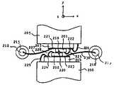
본 발명의 실시예를 도면과 함께 설명한다. 제 1a 도는 본 발명에 의한 반도체 레이저 장치의 제 1 실시예를 도시하는 평면도이며, 제 1b 도는 그 측면도, 제 2a 도는 제 1a 도 중심부의 확대 평면도, 제 2b 도는 그 측면도이다.An embodiment of the present invention will be described with reference to the drawings. FIG. 1A is a plan view showing a first embodiment of a semiconductor laser device according to the present invention. FIG. 1B is a side view thereof, FIG. 2A is a magnified plan view of the center of FIG. 1A, and FIG. 2B is a side view thereof.
제 1a 도, 제 1b 도에 도시하는 제 1 실시예는 광 디스크 장치용의 반도체 레이저 장치이다. 제 1a 도 내지 제 2b 도에 있어서, 반도체 레이저 칩(1) 및 (2)는 각각 서브 마운트(9) 및 (10)에 탑재되고, 또 서브 마운트(9)는 마운트(30)을 거처서 블럭(31)에 탑재되며, 서브 마운트(10)은 직접 블럭(31)에 탑재되어 있다. 또, 레이저 광 모니터용의 포트 다이오드(21)도 마찬가지로 블럭(31)에 탑재되어 있다. 단자(23), (24), (25)는 각각 글라스(27), (28), (29)에 의해 기체(34)에 기밀 접착되어 있다. 블럭(31)과 렌즈(32)를 끼워넣은 캡(33) 및 단자 (26)은 기체(34)에 용접되어 있다.The first embodiment shown in Figs. 1A and 1B is a semiconductor laser device for an optical disk device. 1A to 2B, the
상기 기체(34)에는 나사구멍(35), (36)이 열려져 있고, 상기 블럭(31) 및 각 단자(23), (24), (25), (26)을 포함하는 중심부분(37)은 상기 캡(33)과 기체(34)에 의해 기밀 봉지되어 있다.Screw holes 35 and 36 are opened in the
상기 반도체 레이저 칩(1)은 발진파장 780nm의 AlGaAs계 반도체 레이저이고, 저잡음 특성을 가지며 광 디스크의 재생에 사용된다. 레이저 광은 제 2a 도에 도시하는 활성층(3)의 위치에서 출사한다. 상기 레이저 칩(1)의 n측이 전극면(5), p측이 전극면(6)이다. 전극면(5)와 활성층(3)의 거리는 약 5μm이다.The
한편, 반도체 레이저 칩(2)는 발진파장 830mm의 AlGaAs계 반도체 레이저이고, 고출력 특성을 가지며 광 디스크의 라이트 소거에 사용된다. 반도체 레이저 핍(2)의 p측이 전극면(7), n측이 전극면(8)이다. 레이저 광은 전극면(7)에서 약 5μm 떨어진 활성층(4)의 위치에서 출사한다.On the other hand, the
서브 마운트(9) 및 (10)은 SiC 세라믹스로 되고 그 표면에는 전기 배선을 위해 부분적으로 Au/Ni/Ti의 메털라이즈를 시행하고 있다{메털라이즈 면은(11), (12), (13), (14)}.The
포토 다이오드(21)은 0.8μm 파장대 SiPIN 포토 다이오드에서 상면은 수광면으로 되어 있고, 상기 반도체 레이저 칩(1) 및 (2)에서 출사하는 레이저 광의 광 파워를 다음에 기술하는 바와 같이 시분할로 모니터 한다.In the
레이저 광의 출사 각도는 10∼40°로 넓으며 포토 다이오드(21)에는 양쪽의 반도체 레이저에서의 광이 입사하므로 공간적으로는 2개의 레이저 광이 분리해 있지 않다. 따라서, 이 상태대로는 각각의 레이저 광의 광 파워를 독립으로 모리터하는 것은 불가능하다. 그래서, 특정한 시간 영역내에 1개씩 차례로 반도체 레이저를 발진시키는 것에 의해 1개의 포토 다이오드를 사용해서 각각의 레이저 광의 광 파워를 시간적으로 분리하여 독립으로 모니터할 수가 있다. 예를들면, 계산기용 코드 데이타 기록 광 디스크의 경우는 트랙 1개에 1개소에 있는 교대 섹터 또는 여러개 트랙에 1줄 있는 교대 트랙상을 광 스포트가 주행하고 있는 시간이나, 비디오용 광 디스크의 경우는 트랙 1둘레에 1개소 있는 수직동기, 귀선기간이 레이저 광의 파워 모니터용의 시간영역으로써 이용할 수 있다. 이 시간 영역내에 먼저 한쪽의 반도체 레이저만을 발진시켜 광 파워를 모니터하고, 다음에 또 한쪽의 반도체 레이저만을 발진시켜 광 파워를 모니터하면, 각각의 레이저 광의 파워 모니터를 시분할 독립으로 행할 수 있다.The emission angle of the laser light is wide at 10 to 40 °, and since light from both semiconductor lasers is incident on the
단자(23), (24), (25), (26), 마운트(30), 블럭(31), 캡(33) 및 기체(34)의 재료는 예를들면 코발트 또는 Cu로 이들의 표면에는 Au/Ni 도금이 되어 있다. 렌즈(32)는 예를들면, 양면 비구면 글라스 렌즈이다. 레이저 광의 빔 특성이나 광학계의 규격에 의해서 렌즈(32)의 표면 형상은 회전 대상의 타원면, 포물면, 쌍곡면 또는 회전비대상의 곡율 반경을 갖는면 형상 또는 그들을 합성한 면 형상에 가공된다. 상기 렌즈(32)에 의해 반도체 레이저 칩(1) 및 (2)에서 출사한 레이저 광은 구면수차가 보정된 한쪽으로 치우치지 않은 평행빔으로 되어서 반도체 레이저 장치에서 출사한다. 평행광속으로 할 필요가 없을 경우나 평행광속으로 하는 광학계를 별도로 마련할 경우에는 상기 렌즈(32)를 설치할 필요가 없는 것은 물론이다.The materials of the
반도체 레이저 칩(1) 및 (2)와 서브 마운트(9) 및 (10), 서브 마운트(9)와 마운트(30), 서브 마운트(10)과 블럭(31), 마운트(30)과 블럭(31), 포토 다이오드(21)과 블럭(31) 각각의 사이는 모두 접착을 땜납으로 행하고, 조립공정에 따라서 각각 융점이 다른 땜납 예를들면, Au-Sn, Pb-Sn, In-Sn합금등을 사용하였다.
반도체 레이저 칩(1), (2)의 전기 배선은 다음과 같이 행하였다. 전극면(5)는 와이어(15)에서, 메털라이즈면(12)는 와이어(16)을 거쳐서 단자(23)에 접속하고, 전극면(6)은 메털라이즈면(11) 및 와이어(17)을 거쳐 마운트(30) 및 블럭(31), 기체(34)를 각각 경유해서 단자(26)에 접지되어 있다. 전극면(7)은 와이어(18), 메틸라이즈면(13), 와이어(19), 블럭(31), 기체(34)를 각각 거쳐서 단자(26)에 접지되어 있다. 전극면(8)은 메털라이즈면(13), 와이어(20)을 거쳐서 단자(24)에 접속되어 있다. 포토 다이오드(21)의 수광면 측은 와이어(22)를 거쳐서 단자(25)에 접속하고, 반대측은 블럭(31), 기체(34)를 거쳐서 단자(26)에 접지되어 있다. 와이어(15), (16), (17), (18), (19), (20), (22)는 모두 Au선이다.The electrical wiring of the
다음에, 본 반도체 레이저 장치를 조립하는 대략적인 공정을 설명한다. 우선 포토 다이오드(21)을 블럭(31)의 소정의 위치에 Au-Sn 땜납에 의해 접착해 놓는다. 다음에, 반도체 레이저 칩(1), (2)를 각각 서브 마운트(9), (10)에 Au-Sn 땜납에 의해 접착한다. 서브 마운트(9)를 마운트(30)의 소정 위치에 또, 서브 마운트(10)을 블럭(31)의 소정 위치에 Pb-Sn 땜납에 의해 접착한다. 그리고 마운트(30)을 블럭(31)에 밀착시켜서 가로로 움직이게 하면서 활성층(4)에 대한 활성층(3)의 위치를 조절한 후 In-Sn 땜납에 의해 고정한다. 블럭(31)은 상기 공정 종료후에 기체(34)에 용접하여도 좋고, 상기 공정 전에 미리 용접해 두어도 좋다. 땜납은 공정의 순서나 반도체 레이저 장치의 내열성의 규격등에 의해서 다른 종류의 땜납을 사용하는 것도 있다.Next, an outline process of assembling the present semiconductor laser device will be described. First, the
또, 반도체 레이저 칩(2)의 부착 위치는 반도체 레이저 칩(1)의 부착 위치보다도 레이저 광 출사 방향으로 수 μm 내지 수십 μm뒤에 비켜서 있다. 이것은 레이저(1), (2)의 파장에 의해서 렌즈(32)의 재료 글라스 굴절율이 상이하므로, 이색 수차를 보정하기 위해서이다. 비켜서는 거리는 렌즈(32)의 굴절율 차가 반도체 레이저(1) 및 (2)의 파장차에 대략 비례하는 것때문에 마찬가지로 파장차에 대략 비례한다. 조립 공정에 있어서, 반도체 레이저 칩(2)를 서브 마운트(10)에 부착할 때에 미리 비켜서 놓으면, 나중에는 반도체 레이저 칩(1), 서브 마운트(9), (10), 마운트(30), 블럭(31)의 상면을 각각 가지런히 맞추어서 조립해 가면 된다.In addition, the attachment position of the
상기 본 실시예에 의한 광 디스크용 광학 헤드에서는 리얼 타임에서 저잡음 재생과 고출력 라이트 소거가 가능하다. 그리고도, 2개의 반도체 레이저 칩에 대해서 동일한 광학계에서 끝나기 때문에 광학 헤드를 소형으로 할 수가 있다.In the optical head for an optical disc according to the present embodiment, low noise reproduction and high output light erasing are possible in real time. In addition, since the two semiconductor laser chips end in the same optical system, the optical head can be made compact.
또한, 본 실시예에서 기술한 바와같이, 한쌍의 반도체 레이저 칩(1), (2)는 공간을 두고 서로 마주대한 2개의 면(11), (13)에 각각 분리해서 고착하여 전극면(5), (7)를 대략 평행으로 또한 대향하는 위치로 배치하면, 활성층(3), (4) 사이의 간격 즉, 발광 스포트 간격을 용이하게 50μm로 할 수가 있다. 따라서, 유효시야가 보다 작은 소형 렌즈를 사용할 수 있기 때문에, 광학 헤드를 보다 더 경량 소형화할 수 있다. 여기에서, 발광 스포트 간격을 50μm로 하여도 반도체 레이저 칩(1)과 (2)는 전기적으로 완전히 분리되어 있으며, 또한 각각 오목자 형의 블럭(31)의 떨어진 위치에 부착되어 있으므로, 상기 레이저(1)과 (2)는 전기적으로도 열적으로도 서로 간섭하는 일이 없고, 따라서 종래의 반도체 레이저 장치와 달리 필요 이상의 간섭대책을 시행할 필요가 없다.In addition, as described in the present embodiment, the pair of
또, 2개의 반도체 레이저 칩(1), (2)의 발진파장이 상이하므로, 신호 검출계에 있어서 2줄의 레이저 빔의 신호 분리를 광학 파장 필터를 사용해서 파장 분리하는 것만으로 간편하게 행할 수가 있다. 이 때문에, 발진파장이 같을 경우의 복잡한 광학계를 생략할 수가 있다.In addition, since the oscillation wavelengths of the two
상기한 점에서 본 실시예에 의하면 광 디스크용 광학 헤드의 크기를 종래의 1/2 이하도 소형화할 수 있고 그리고도, 가동부 광학계의 경량화에 의해 액추에이터의 고속 동작이 가능하게 되어 광 디스크의 액세스 시간이 약 30% 단축된다.In view of the foregoing, according to the present embodiment, the optical head for optical disks can be made smaller than 1/2 of the size of the conventional optical disks, and the actuator can be operated at high speed by reducing the weight of the moving part optical system. This is reduced by about 30%.
본 제 1 실시예의 반도체 레이저 장치를 광 디스크 장치에 응용한 예를 제 3 도에 도시한다. 반도체 레이저 장치(71)의 내부에는 발진파장이 830nm에서 고출력인 레이저 칩(101) (이하, LD1라 칭한다)과 780nm의 저잡음인 레이저 칩(102) (이하 LD2라 칭한다)의 2개의 반도체 레이저 칩이 제 1 실시예에 도시한 바와같이 근접해서 배치되어 있다(오른쪽 위의 원내에 부분확대도를 도시한다). 상기 2개의 반도체 레이저 칩 LD1 및 LD2에서 출사한 광은 조준렌즈(72) 및 빔 정형 광학계(73)을 통하는 것에 의해서 원형 강도 분포를 갖는 평행 광속으로 된다. 여기에 사용한 반도체 레이저 장치(71)의 캡에는 렌즈 대신에 평판 글라스가 끼워 넣어져 있다. 여기에서, 빔 정형 광학계(73)은 규격에 의해 생략할 경우도 있다. 평행 광속은 빔 스플리터(74),λ/4판(75)를 통과하여, 조리개 렌즈(76)에 의해서 광 디스크(77)상의 기록막(701)에 직경 약 1μm의 집광 스포트로써 조여 들어간다.3 shows an example in which the semiconductor laser device of the first embodiment is applied to an optical disk device. Inside the semiconductor laser device 71 are two semiconductor laser chips, a laser chip 101 (hereinafter referred to as LD1) having a high output at 830 nm and a laser chip 102 (hereinafter referred to as LD2) having a low noise of 780 nm. As shown in this first embodiment, they are arranged in close proximity (showing a partial enlargement in the circle on the upper right). The light emitted from the two semiconductor laser chips LD1 and LD2 passes through the aiming
LD1의 집광 스포트 SP1은 LD2의 집광 스포트 SP2에 대해서 회전하는 광 디스크(77)의 트랙(84)상에서 선행하고 있고, SP1에서 정보의 기록(라이트, 소거), SP2에서 재생이나 에러 체크를 행한다(왼쪽 아래의 원내에 부분 확대도를 도시한다).The condensing spot SP1 of LD1 is preceded on the track 84 of the
광 디스크(77)의 트랙(84)에 있어서, 상기 SP1과 SP2의 간격 D1은 LD1과 LD2의 발광 스포트 간격 d1과 조준 렌즈(72)의 조리개 렌즈(76)으로 되는 조리개 광학계의 횡의 증배율 m1로 구하여진다. 조준 렌즈(72)의 초점 거리를 fc, 조리개 렌즈(76)의 초점 거리를 fF로 하면 조리개 광학계의 횡의 증배율 m1은In the track 84 of the
m1= fF/ fC.............................................................................. (1)m1 = fF / fC ......................... .................................... (One)
로 된다. 따라서, 광 디스크(77) 상에서의 집광 스포트 간격 D1과 반도체 레이저의 발광 스포트 간격 d1의 관계는It becomes Therefore, the relationship between the condensing spot spacing D1 on the
D1= m1d1= (fF/fC)d1............................................................... (2)D1 = m1 d1 = (fF / fC ) d1 ................................. .............................. (2)
에서 주어진다. 광 디스크 장치에 있어서 D1의 규격은 조리개 렌즈(76)의 상의 시야, 신호 처리 방식, 디스크 포매트 등을 고려해서 결정된다. 실제로 D1은 50μm 이하, 바람직하게는 20μm 이하로 설정되는 경우가 많다. 그런데, 조리개 광학계에는 색수차가 있기 때문에 파장이 다른 레이저 광을 같은 광학계에서 조여들면 집광 스포트 SP1과 SP2의 초점위치가 레이저 광 진행방향에 어긋난다. 초점 제어는 어느것인가 한쪽의 집광 스포트에서 행하기 때문에 다른쪽의 집광 스포트는 초점 어긋남을 일으키는 것으로 된다. 상기 초점어긋남이 생기지 않도록 하기 위해서는, 미리 LD1과 LD2를 레이저 광 출사 방향에 대해서 앞뒤로 어긋나게 해서 설치하여 2개의 레이저의 발광 스포트를 광축 방향으로 어긋나게 해두면 된다. 여기에서, 조리개 렌즈(76), 조준 렌즈(72)로 되는 조리개 광학계 전체의 색수차가 C(μm/nm), LD1, LD2 사이의 발진파장 차가 △λ(nm)이면 처음의 초점 위치의 어긋남 D2는Is given in In the optical disk apparatus, the standard of D1 is determined in consideration of the field of view of the
D2= △λ·C ....................................................................... (3)D2 = Δλ · C ..................................... (3)
로 된다. 조리개 광학계의 종상의 배율 m2는It becomes The vertical magnification m2 of the aperture optical system is
m2= (fF/fC)2.......................................................................... (4)m2 = (fF / fC )2 ... ................................... (4)
이기 때문에 LD1과 LD2의 부착 위치가 필요한 어긋남량 d2는Therefore, the shift amount d2 that requires the attachment position of LD1 and LD2 is
d2= D/m2= (△λ·C)/ (fF/ fC)2............................................(5)d2= D / m2= (△ λC) / (fF/ fC)2............................................(5)
에서 주어진다. 이것에 의해 LD1을 레이저 광 출사 방향에 대해서 LD2보다도 d2만 뒤에 부착해 두면 LD1, LD2의 광 디스크(77) 사이에서의 초점 위치는 일치한다. 단, d2의 값은 LD1, LD2의 양쪽에 비점수차가 없는 경우의 값이다.Is given in For the LD1 As a result the laser light emitting direction than LD2 d2 Keeping attached behind only the focal position between the LD1, LD2 of the
실제로는 사용한 발진파장 780nm의 레이저 LD2가 비점수차를 갖고 있었기 때문에 d2를 보정할 필요가 있다. LD2의 발광점(최소 착란원의 중심위치로 생각한다)은 비점격차의 1/2만 레이저 끝면에서 레이저 칩내부로 들어가 있다고 생각되므로, LD2의 비점격차를 △Z로 하면 LD1과 LD2의 부착위치의 어긋남량 d2'는In practice, d2 must be corrected because the laser LD2 having the oscillation wavelength of 780 nm used has astigmatism. Since the light emitting point of LD2 (which is considered as the center of the confusion circle) is only 1/2 of the non-point difference, it is considered that the laser tip enters the laser chip inside the laser tip. The deviation of d2 ' is
d2'= d2+ (△Z/2) .................................................................. (6)d2 ' = d2 + (△ Z / 2) ..................... ............................. (6)
로 된다. LD1, LD2의 양쪽에 비점수차가 있을 경우는It becomes If there is astigmatism between both LD1 and LD2
d2"= d2+ (△ZS-△ZL) / 2d2 " = d2 + (△ ZS- △ ZL ) / 2
로 된다. 단, △ZS는 단파장으로 발진하는 LD2의 비점격차, △ZL은 장파장으로 발진하는 LD1의 비점격차이다.It becomes However, ΔZS is the non-point difference of LD2 oscillating at short wavelength, and ΔZL is the non-point difference of LD1 oscillating at long wavelength.
다음에, 집광 스포트 간격 D1과 LD1, LD2의 위치어긋남량 d2를 (2), (6)식을 사용하여 계산한다.Next, the position shift amount d2 of the condensing spot spacing D1 and LD1 and LD2 is calculated using the formulas (2) and (6).
예를들면, fF=3.3mm, fC=8.75mm, d1=50μm, C =0.05μm/nm, Δλ = 830-780 =50nm, ΔZ =16μm의 경우 D1=19μm, d2'=26μm이다. 상기 D1의 값은 광 디스크의 리얼 타임 기록 재생을 행하는데 충분히 적합한 것이다. 상기 d2"의 값은 LD1과 LD2를 반도체 레이저 장치에 고착하는 공정에 있어서, 충분하게 제어가능한 값이다. 실제로 상기의 수치에 따라서 광 디스크 장치를 조립한 바, SP1과 SP2의 초점 거리는 일치해 있고 양호한 집광 스포트 특성이 얻어지고 있다.For example, fF = 3.3mm, fC = 8.75mm, d1 = 50μm, C = 0.05μm / nm, Δλ = 830-780 = 50nm, ΔZ = 16μm, D1 = 19μm, d2 ' = 26 μm. The value of D1 is sufficiently suitable for real time recording and reproducing of an optical disc. The value of d2 " is a sufficiently controllable value in the process of fixing LD1 and LD2 to the semiconductor laser device. In fact, when the optical disk device is assembled according to the above numerical values, the focal length of SP1 and SP2 is Matching and good condensing spot characteristics are obtained.
광 디스크(77)에서 반사한 2개의 파장 광은 빔 스플리터(74)에서 반사되어 광학 파장 필터(78)에 의해서 파장 분리된다. 예를들면, 파장 λ=830nm은 전투과, 파장λ=780nm은 전반사의 광학 파장 필터를 사용한 경우는 검출 광학계(79)에는 λ=830nm의 광만이, 검출 광학계(80)에는 λ=780nm의 광만이 입사한다. 파장 분리 특성을 더욱 향상시키기 위해서는 (1) 광학 파장 필터(78)를 2매 사용하고, 또는 (2) 양면에 파장 분리막이 부착된 필터를 사용하는 등의 방법을 취하면 좋다. 검출 광학계(79)의 출력은 신호처리 회로(81)로 들어가고, 오토 포커스나 트래킹등의 광점 제어신호 또는 디스크상에 미리 기록되어 있는 어드레스 정보등을 얻는다. 한편, 검출 광학계(80)의 출력은 신호처리 회로(82)로 들어가 기록의 재생이나 에러 체크를 행한다. 반도체 레이저 장치(71)은 구동회로(83)에 의해서 제어된다.The two wavelength light reflected by the
기록시 LD1은 기록(라이트, 소거)정보에 따라서 구동회로(83)에 의해 펄스 변조되고, LD2는 저출력에서 직류 구동되어 신호처리 회로(81)에 의해서 광점 제어하면서 신호처리 회로(82)에 의해서 에러 체크를 행한다. 재생시 LD1, LD2모두 저출력에서 직류 구동시켜 신호처리 회로(81)에서 광점 제어신호를 얻으면서 신호처리 회로(82)에서 재생신호를 얻는다. 재생에서는 LD1을 발진시키지 않고서 LD2만으로 광점 제어와 재생과의 양쪽을 행하는 방식도 있다. LD1, LD2나 신호처리 회로(81), (82)의 역할은 신호 처리방식이 상이함에 의해서 변경할 수 있다.At the time of writing, LD1 is pulse-modulated by the
상기 광 디스크 장치의 실시예에 있어서 LD2로써 사용한 발진파장 780nm의 저잡음 레이저는 고주파 중첩등의 수단을 사용하지 않아도 좋다는 점에서 신호 재생에 적합해 있지만, 반면 종래로부터 비점수차가 크다는 단점이 있었다. 이 단점에 대해서는 조준 렌즈(72)의 열림 구멍수를 예를들면, 0.2이하로 하는 것에 의해서 충분히 대처할 수 있으므로 광 디스크 장치로써는 문제가 없다.In the embodiment of the optical disk device, the low-noise laser of 780 nm oscillation wavelength used as LD2 is suitable for signal reproduction in that it is not necessary to use means such as high frequency superposition, but has a disadvantage in that astigmatism is large. This disadvantage is sufficiently addressed by setting the number of opening holes of the aiming
이상, 본 발명의 제 1실시예와 이것을 광 디스크 장치에 응용한 예에 대하여 기술하였다. 본 발명의 주안점은 2개의 반도체 레이저 발광 스포트 간격을 좁히기 위해서 반도체 레이저의 활성층에 가까운 측의 전극면끼리 대향시키는 것과 같은 형태로 배치한 것에 있으므로, 본 발명은 상기한 구성 부품이나 규격, 방식등에 의해서 한정되는 것은 아니다. 용도에 따라서 반도체 레이저나 다른 주변 부품의 규격을 변경하는 것이 가능하다. 본 실시예에 있어서, 1쌍의 반도체 레이저 칩이 각각 분리해서 고착되어 있는 2개의 면은 반드시 평행한 2평면으로는 한정하지 않고, 서로 경사진 면이나 곡면상에 반도체 레이저 칩이 고착되는 것도, 반도체 레이저 장치에 이어지는 광학계의 규격등의 때문에 경우에 따라서는 있을 수 있다.In the above, the first embodiment of the present invention and an example in which this is applied to an optical disk device have been described. The main point of the present invention is to arrange the electrode faces on the side close to the active layer of the semiconductor laser so as to narrow the gap between the two semiconductor laser emission spots. It is not limited. It is possible to change the specifications of semiconductor lasers and other peripheral components depending on the application. In the present embodiment, the two surfaces on which the pair of semiconductor laser chips are separated and fixed to each other are not limited to two parallel planes, but the semiconductor laser chips are also fixed to the inclined surfaces or curved surfaces. In some cases, such as because of the specification of the optical system following the semiconductor laser device.
또, 면상으로의 반도체 레이저 칩의 고착위치는 임의로 선택할 수 있다. 본 실시예에서 사용한 블럭은 오목자형을 하고 있지만, 조립공정이나 조립장치등의 형편에 따라 다른 구조의 블럭 형성, 예를들면 4각 기둥형 블럭을 2개 사용할 경우도 일어날 수 있다. 본 실시예에서는 2개의 반도체 레이저로써 발진파장 780nm 저잡음 레이저와 830nm 고출력 레이저를 사용했지만 이들 특성의 조합은 임의이다. 파장, 출력, 잡음 특성이 같은 경우도 목적에 의해서 있을 수 있다. 또, 2개의 레이저 발광 분포가 다른것이라도 좋다. 추기형이나 광 자기형, 광 디스크에 한정하지 않고, 반도체 레이저의 한쪽을 급냉 기록용 또, 한쪽을 서냉 소거용으로써 상 변화형 가역 광 디스크에도 본 발명은 당연히 응용가능하다. 포토 다이오드에 관해서는 차폐판등을 사용해서 2개의 레이저 빔을 공간적으로 분리하여 2개의 레이저 파워를 독립으로 모니터할 수도 있다. 또, 본 발명의 용도는 광 디스크에 한정하는 것이 아니고 예를들면, 본 실시예와 마찬가지의 구성에서 발광 스포트 간격을 보다 근접시켜 렌즈를 적당한 초점 거리의 것으로 바꾸면, 본 발명을 파장 다중 광 통신에 사용할 수도 있다. 또한, 반도체 레이저 칩 대신에 끝면 발광형 발광 다이오드등의 발광 소자를 사용하거나, 반도체 레이저와 포토 다이오드나 이들의 구동 회로를 집적한 광 전자 직접회로(Opto Electronic Integrated Circuits, 약칭 OEIC)를 사용하여도 본 발명의 효과가 충분히 발휘되는 것은 물론이다.In addition, the fixing position of the semiconductor laser chip on the surface can be arbitrarily selected. The block used in this embodiment has a concave shape, but may also occur in the case of forming a block having a different structure depending on circumstances such as an assembling process or an assembling device, for example, using two quadrangular pillar blocks. Although the oscillation wavelength 780 nm low noise laser and 830 nm high output laser were used as two semiconductor lasers in this embodiment, the combination of these characteristics is arbitrary. The same wavelength, output, and noise characteristics may be due to the purpose. Moreover, two laser emission distributions may differ. The present invention is naturally applicable to a phase change type reversible optical disc by not only being a write-once type, a magneto-optical type or an optical disc, but also one of the semiconductor lasers for quench recording and one for slow cooling erase. As for the photodiode, two laser beams may be spatially separated using a shielding plate or the like to monitor two laser powers independently. In addition, the use of the present invention is not limited to the optical disk. For example, in the same configuration as that of the present embodiment, when the lens is replaced with a suitable focal length, the light emission spot spacing is closer to the wavelength multiplex optical communication. Can also be used. In addition, instead of using a semiconductor laser chip, a light emitting device such as an end emitting light emitting diode may be used, or an optoelectronic integrated circuit (OEIC) integrated with a semiconductor laser and a photodiode or a driving circuit thereof may be used. It goes without saying that the effect of the present invention is sufficiently exhibited.
제 4 도에 도시하는 제 2 실시예는 광 디스크 병렬 전송용 반도체 레이저 장치를 설명하는 것이다. 상기 제 1 실시예를 4개 나란히 서 있는 것과 같은 구성으로 되어 있다. 8개의 반도체 레이저(38), (39)는 각각 2개의 서브 마운트(40)을 거쳐서 2개의 블럭(41)에 적재되어 있다. 전기적으로는 8개의 반도체 레이저(38), (39)에서 서브 마운트(40)상의 부분 메털라이즈면(도시하지 않음)과 8줄의 와이어를 거쳐서 각각 8개의 단자(42)에 접속되어 있고, 레이저의 독립 변조가 가능하다. 같은 열에 있는 4개의 레이저(38)은 발진파장 780nm의 저잡음 레이저, 다른 열의 4개의 레이저(39)는 발진파장 830nm의 고출력 레이저이다. 레이저(38)과 레이저(39)의 상대하는 것끼리의 조합으로 레이저 4개의 쌍이 이루어진다. 1쌍의 레이저에 대해서 보면 공간을 두고 서로 마주 대하는 2개의 면에 각각 레이저가 분리해서 고착되어 있고, 레이저의 전극면끼리는 대향하는 것과 같은 형태로 배치되어 있다. 상대한 1쌍의 반도체 레이저로 제 1 실시예와 마찬가지로 광 디스크의 리얼 타임 기록 재생을 행한다. 인접하는 같은 발진파장의 레이저끼리는 각각 광 디스크의 제각기 다른 위치를 트래킹하고 있다. 또, 각 레이저의 부착위치는 물론 색수차나 광 디스크의 트랙 피치등을 고려해서 배치하였다. 레이저(38)의 열과 레이저(39)의 열이 경사지게 어긋나고 있는 것도, 트래킹 위치 조정을 위한 것이다.The second embodiment shown in FIG. 4 describes a semiconductor laser device for optical disk parallel transmission. The first embodiment has the same configuration as standing four side by side. Eight
본 실시예에 의하면, 광 디스크의 4개의 트랙을 동시에 기록 재생할 수가 있어 4병렬 전송이 가능하게 되므로, 전송 속도가 4배 고속으로 되는 효과가 있다. 또한, 레이저의 갯수를 멀티화하면 보다 더 전송 속도가 향상하는 것은 말할 것도 없다.According to this embodiment, since four tracks of the optical disc can be recorded and reproduced at the same time and four parallel transmission is possible, there is an effect that the transmission speed is four times higher. It goes without saying that multiplying the number of lasers further improves the transmission speed.
제 5 도에 도시하는 제 3 의 실시예의 반도체 레이저 장치는 2개의 반도체 레이저(43), (44)가 활성층(45), (46)에 가까운 쪽의 전극면(48), (49)가 서로 접착되어 일체화 되고 있다. 전극면(50)은 마운트(52)의 표면의 메털라이즈면(51)에 접착된다. 전극면(47), (49), 메털라이즈면(51)은 각각 와이어(52), (54), (55)에 의해서 단자(56), (57), (58)에 전기접속된다. 단자(57)을 접지로 취하면 레이저(43) 및 (44)의 독립변조가 가능하다. 본 실시예에 의하면 반도체 레이저(43), (44)의 동시 발진 상태, (43)의 발진상태, (44)의 발진상태, 무발진 상태의 4개의 상태에 의해 2비트의 정보를 송신하는 것이 가능하고, 예를 들면 광 통신에 사용된다. 또, 반도체 레이저(43), (44)의 발진파장을 상이하게 하면 파장 다중 광 통신에도 적용할 수 있다. 또 동시 발진시키면 1개의 장치로 종래의 2배의 광 출력을 낼 수가 있고, 고출력 반도체 레이저 장치로써도 유효하였다.In the semiconductor laser device of the third embodiment shown in FIG. 5, two
제 6 도에 도시하는 제 4 실시예는 레이저 빔 프린터용 반도체 레이저 장치이다. 마운트(66) 및 (67) 상에 각각 적재된 반도체 레이저(59) 및 (60)이 절연층(63)을 거쳐서 접착되어 있다. 상기 반도체 레이저(59) 및 (60)은 어느것도 발진파장 830nm의 AlGaAs계의 고출력 레이저이다. 상기 절연층(63)에는 저열전도성의 전기 절연재를 사용하였다. 또, 레이저(59) 및 (60)은 좌우 대칭은 아니고 활성층(61) 및 (62)의 위치가 중심에서 치우치고 있지만, 이것은 레이저(59) 및 (60)의 칩 형성시에 있어서의 절단을 상기 활성층(61), (62)에 왜곡의 열화가 생기지 않을 정도로 고의로 어긋나게 해서 행한 것이다. 이것에 의해, 전기배선용의 와이어(64), (65)가 본딩하기 쉽게 되었다.A fourth embodiment shown in FIG. 6 is a semiconductor laser device for a laser beam printer. The
본 실시예에 의하면 종래의 반도체 레이저 장치에서는 불가능하였던 발광 스포트 간격이 얻어진다. 즉, 활성층(61), (62)의 도면의 세로방향의 간격을 10μm, 도면 가로방향의 간격을 약 50μm로 할 수가 있었다.According to this embodiment, a light emission spot interval that is impossible with the conventional semiconductor laser device is obtained. That is, the intervals in the longitudinal direction of the drawings of the
본 장치를 사용해서 레이저(59), (60)을 독립 변조시키면서 도면 가로방향으로 레이저 빔을 주사시키면 1스캔에서 2행의 프린트를 행할 수가 있어 종래의 1레이저 빔 프린터에 비해서 프린트 속도가 2배 고속으로 된다. 또, 발광 스포트 간격이 충분히 작으므로, 본 장치에 연결되는 주사 광학계의 크기는 1레이저 빔의 경우와 거의 변하지 않고, 경량 소형으로 할 수 있다.When the laser beam is scanned in the horizontal direction of the drawing while independently modulating the
그런데 2개의 레이저(59), (60)은 절연층(63)을 거쳐서 접착되어 있고, 또한 열의 발생원인 활성층(61) 및 (62)는 약 50μm 떨어져 있으므로, 상기 레이저(61), (62) 사이의 열적 및 전기적인 간섭은 일어나지 않는다. 단, 활성층을 50μm 떨어지게 했기 때문에 프린트를 행할때에 2개의 레이저(59), (60)의 변조의 동기를 취할 필요가 있다. 이 때문에 제어계에 포토 다이오드를 사용하였다. 상기 포토 다이오드의 수광면을 2줄의 주사빔이 통과하면 2개의 전기 펄스가 발생한다. 상기 2개의 전기 펄스 사이의 시간차는 활성층(59), (60)의 도면 가로방향의 간격에 대응하기 때문에 이 시간차의 분 만큼 레이저(59), (60) 사이의 변조 타이밍을 어긋나게 해서 조절해 주면 동기를 행하는 것이 가능하다.By the way, the two
또, 본 실시예의 장치를 멀티화하면 더욱 레이저 빔 프린터의 고속화를 실현할 수 있는 것은 물론이다. 또, 본 실시예는 레이저 빔 프린터에 한정하지 않고, 광 디스크나 광 통신등의 광 정보 처리 장치에도 응용할 수가 있다.Moreover, it goes without saying that the speed of the laser beam printer can be further increased by multiplying the apparatus of this embodiment. The present embodiment is not limited to a laser beam printer, but can also be applied to optical information processing devices such as optical disks and optical communications.
다음에, 본 발명의 제 5 실시예를 제 7 도, 제 8 도, 제 9 도를 사용하여 설명한다.Next, a fifth embodiment of the present invention will be described with reference to FIGS. 7, 8, and 9.
제 5 실시예에서는 제 1 실시예의 반도체 레이저 장치와 비교해서 2개의 반도체 레이저 칩의 전극면끼리 서로 대향하도록 배치했다는 점에서는 마찬가지이지만, 반도체 레이저 장치의 패케이지 구조가 약간 다르고, 제 1 실시예보다도 또 2개의 반도체 레이저 칩의 고정밀도 위치 결정 조립이 행하기 쉬운 구조로 되어 있다.The fifth embodiment is the same in that the electrode faces of the two semiconductor laser chips are arranged to face each other as compared with the semiconductor laser device of the first embodiment, but the package structure of the semiconductor laser device is slightly different, compared to that of the first embodiment. Moreover, it has a structure which is easy to perform high precision positioning assembly of two semiconductor laser chips.
본 제 5 실시예는 예를들면, 리라이트형 광 디스크 장치의 리얼 타임 소거, 기록, 재생용으로 사용된다.This fifth embodiment is used, for example, for real time erasing, recording and reproduction of a rewrite type optical disk device.
제 7 도는 본 제 5 실시예의 반도체 레이저 장치의 전체 사시도이다. 제 8 도는 그 중심부의 정면도이다.7 is an overall perspective view of the semiconductor laser device of the fifth embodiment. 8 is a front view of the central portion thereof.
제 9 도는 본 반도체 레이저 장치의 조립장치를 도시하는 도면이다.9 is a diagram showing an assembling apparatus of the present semiconductor laser device.
제 7 도, 제 8 도에 있어서, 레이저(201), (202)는 서브 마운트(203), (204)를 거쳐서 블럭(205), (206)에 부착되어 있다. 블럭(205), (206)은 땜납(207), (208)에 의해서 기체(209)에 고정되어 있다. 단자(212), (213)은 글라스(215), (216)에 의해서 기체(209)에 기밀 접착되고, 기체(209)는 전기 절연되어 있다. 단자(214)는 기체(209)에 용접된 접지 단자이다. 기체(209)에 열려진 구멍(217), (218)은 본 반도체 레이저 장치 부착용이 나사 구멍이다. 레이저(201), (202), 서브 마운트(203), (204), 블럭(205), (206)등의 중심 부분은 캡(210)과 창(211)에 의해서 기밀봉지되어 있다.7 and 8, the
레이저(201)은 발진파장 830nm의 고출력 기록, 소거용 AlGaAs계 반도체 레이저, 레이저(202)는 발진파장 780n의 저잡음 재생용 AlGaAs계 반도체 레이저이다. 레이저(201), (202)의 공진기의 길이는 약 300μm, 소자의 두께는 약 100μm이다. 레이저(201), (202)는 와이어(225), (228)을 끌어내기 쉽게 하기 위해서 활성층(219), (220) (즉, 발광 스포트)의 위치를 레이저 칩의 중심에서 비켜서 칩을 절단하였다(제 8 도).The
서브 마운트(203), (204)는 SiC 세라믹스(전기절연체)로 되고, 두께는 약 200μm이다. 서브 마운트(203), (204)에는 레이저(201), (202)의 구동용의 전기 배선을 행하기 위해서 부분적으로 Au, Ni, Ti의 메털라이즈(221), (222), (223), (224)가 행해지고 있다. 레이저(201), (202)의 상부 전극은 각각 와이어(225), (228), 메털라이즈 (222), (224), 와이어(226), (229)를 거쳐서 블럭(205), (206)에 전기접속되어 접지(단자 214)에 연결되어 있다. 레이저(201), (202)의 하부 전극은 각각 메털라이즈(221), (223), 와이어(227), (230)을 거쳐서 레이저 구동용의 단자(212), (213)에 전기접속되어 있다. 와이어(225), (226), (227), (228), (229), (230)에는 모두 Au선을 사용하였다.The
블럭(205), (206)의 재료에는 레이저(201), (202)에서 발생하는 열을 효율 좋게 벗어나기 위해서 열전도율이 높은 Cu를 사용했다. 블럭(205), (206)의 치수는 세로 1.5mm×가로 1.5mm×높이 2.0mm이다.In the materials of the
기체(209), 단자(212), (213), (214) 및 캡(210)은 글라스(215), (216)과 열팽창율이 가까운 코발트합금(열팽창율 5×10⁻⁶℃-1)로 된다.The
창(211)은 레이저(201), (202)에서 출사한 레이저 빔 광을 투과하는 광학 글라스이다. 글라스 면에서 레이저 광의 반사를 방지하기 위해 무반사 코팅을 행하고 있다.The
레이저(201), (202)와 서브 마운트(203), (204) (메털라이즈 221, 223), 서브 마운트(203), (204)와 블럭(205), (206)은 각각 Au-Su 땜납(융점 280℃)에 의해서 고정되어 있다.The
레이저(201), (202)의 위치 맞춤할 때 사용하는 땜납(207), (208)은 Au-Sn 땜납보다도 융점이 낮은 Pb-Sn 땜납(융점 183℃)으로 된다. 블럭(205), (206) 및 기체(209)에는 땜납에 대한 습윤성을 높이기 위해 Au/Ni 도금을 행하였다.The
레이저(201), (202)의 활성층(219), (220)의 상대 위치 즉, 발광 스포트의 상대 위치의 조립 규격은 x, y, z 각 축방향(제 8 도)에 대해서 x=0±1m, y=25±1μm, z=22±2μm로 되어 있다. 이들의 조립 규격은 본 반도체 레이저 장치에 연결하는 광학계에서의 요구에 의해 결정된다. z축 방향에 관해서 레이저(202)의 끝면을 레이저(201)의 끝면보다 22μm 정도 높게한 것은 상기 광학계의 색수차를 보정하기 위해서이다. 또, 여기에 기술한 규격은 반도체 장치에 사용되는 방법에 의해서 변경할 수 있다.The assembly specification of the relative positions of the
제 9 도는 제 5 의 실시예의 반도체 레이저 장치의 조립 장치의 구성도이다. 이 조립 장치는 상기 규격의 반도체 레이저 장치의 최종적인 위치 결정, 고정을 행하는 것이다. 반도체 레이저 장치는 모두 그 위치에 가조립된 상태에서 조립 장치의 히터(234)상에 부착되어 규격을 충족시키도록 조정된 후 조립 장치에서 떼어내진다.9 is a configuration diagram of an assembling apparatus of the semiconductor laser device of the fifth embodiment. This assembling apparatus performs final positioning and fixing of the semiconductor laser apparatus of the said standard. The semiconductor laser apparatuses are all attached to the heater 234 of the assembly apparatus in a state of being preassembled at the position thereof, adjusted to meet the specifications, and then detached from the assembly apparatus.
이하, 조립 장치에 대해서 설명한다. 시료대(232), 미동대(微動坮) (235), (236), 지주(243)은 진동제거대(231)에 단단하게 고정되어 있다. 반도체 레이저 장치가 부착되는 히터(234)는 단열판(233)을 거쳐서 시료대(232)에 고정되어 있다. 기구(239), (240)은 반도체 레이저 장치의 블럭(205), (206)을 체크해서 유지하기 위한 기구이다. 기구(239), (240)은 각각 단열판(237), (238)을 거쳐서 미동대(235), (236)에 부착되어 있다. 반도체 레이저 장치의 상태는 TV 카메라(244)에 의해서 확대 관찰할 수가 있다. 반도체 레이저 장치의 정면상은 대물렌즈(241), 경통(242)를 통해서 TV 카메라(244)의 촬상면에 영사한다. TV 카메라(244)에서 촬영한 영상은 배선(245)에서 영상 처리 장치(246)에 연결하여 배선(247)을 통해서 TV 모니터(248)에 영사되어 나온다. 경통(242)는 지주(243)에 부착되어 있다.Hereinafter, the assembly apparatus will be described. The sample table 232, the moving table 235, 236, and the
다음에 조립 장치에 대해서 상세히 설명한다. 진동 제거대(231)은 견고하고 강성이 높아 우수한 진동제거 특성을 가지므로, 서브 마이크론 오더의 정밀 조립에 적합하다.Next, the assembly apparatus will be described in detail. Since the
히터(234)에는 온도 조절 장치(도시하지 않음)가 연결되어 있고, 설정온도에서 ±1℃ 이내에서 안정하게 유지할 수가 있다. 땜납(207), (208)을 녹일때에는 220℃, 땜납(207), (208)을 굳힐 때에는 170℃로 온도를 설정했다. 히터(234)상면의 실제 온도는 온도 조절 장치에 표시된다. 히터(234)의 재료에는 열팽창율이 작은(〈1×10⁻⁶℃-1) 슈퍼인바 합금을 사용했으므로 온도 변화(50℃=220-170℃)에 의한 히터(234)의 열변위를 ±1μm 이내로 억제할 수가 있었다. 또, 단열판(233)을 사용해서 히터(234)의 열이 시료대(232)에 전해져 열팽창에 의해서 시료대(232)의 위치가 변화하는 것을 방지하였다. 따라서, 조립시에 기체(209)의 위치는 충분히 제어된다. 단열판(233)의 재료는 저열팽창, 단열성 세라믹스(열팽창 계수 -1.3×10⁻⁶℃-1)이다. 또, 땜납(207), (208)의 산화를 방지하기 위해서 땜납(207), (208) 근방은 N2분위기로 하였다.A heater (not shown) is connected to the heater 234 and can be stably maintained within ± 1 ° C at the set temperature. The temperature was set at 220 ° C. when the
그런데, 히터(234)에는 반도체 레이저 장치를 부착하기 위해서 기체(209)를 잡는 기구(도시하지 않음)가 붙어 있다. 또, 반도체 레이저 장치의 단자(212), (213), (214)가 끼워 넣어지도록 소케트(도시하지 않음)를 붙였다. 소케트는 레이저(201), (202) 구동용 전원의 펄스 발생기(도시하지 않음)에 전기접속되어 있다.By the way, the heater 234 is equipped with the mechanism (not shown) which catches the base |
시료대(232)는 x, y, z축 방향으로 거칠은 움직임, 미세한 움직임을 행할 수 있다. 이 시료대(232)에 의해서 히터(234)에 부착한 반도체 레이저 장치 전체의 위치를 움직이게 할 수가 있다.The
기구(239), (240)의 재료는 저열 팽창성의 슈퍼인바 합금으로 했다. 히터(234)의 온도변화(50℃)에 있는 기구(239), (240)의 열변위는 ±0.5μm 이내로 억제되어 있다. 따라서, 조립시에 블럭(205), (206)의 위치 즉, 레이저(201), (202)의 위치를 충분히 제어할 수 있다. 기구(239), (240)이 블럭(205), (206)을 잡을때 척의 개폐에는 전자석을 이용했다. 기구(239), (240)의 선단은 블럭(205), (206)이 유지하기 쉽도록 블럭(205), (206)의 형상에 맞추어서 가공했다. 또, 히터(234)의 열을 미동대(235), (236)으로 전하지 않기 위해 단열판(237), (238)을 사용하였다. 단열판(237), (238)의 재료는 단열판(33)과 같은 저열팽창성, 단열성 세라믹스로 하였다.The materials of the
미동대(235), (236)은 정밀 미동 기구와 피에조 소자에 의해서 x, y, z의 3축에 관해서 ±0.1μm, θx, θy, θz의 3축에 관해서 ±0.1°의 미동 조정을 행할 수가 있다. 미동대(235), (236)을 움직이게 하는 것에 의해서 기구(239), (240)으로 유지한 블럭(205), (206)의 위치를 움직이게 하여 레이저(201), (202)의 활성층(219), (220)의 위치를 앞서 기술한 규격에 맞추어서 조정할 수가 있다.The
또, 기구(239), 단열판(237), 미동대(235)와 기구(240), 단열판(238), 미동대(236)은 좌우 대칭으로 만들어져 있다. 이렇게 하는 것에 의해서, 온도변화(50℃)에 의한 열변위 즉 블럭(205), (206)의 위치 변화는 좌우 대칭으로 일어난다. 레이저(201), (202)의 활성층(219), (220)의 위치 관계는 상대적으로 일치되어 있으면 좋은 것이기 때문에, 대칭으로 일어나는 위치 변화는 조립에 있어서 그다지 문제가 되지 않는다.Moreover, the mechanism 239, the heat insulation board 237, the moving
활성층(219), (220)의 위치 맞춤은 땜납(207), (208)을 용해시킨 상태에서 레이저(201), (202)를 펄스 발생기(도시하지 않음)에 의해서 구동시켜, TV 모니터(248)의 영상을 보고 활성층(219), (220)의 위치(발광 스포트)를 확인하면서 행한다. 영상의 핀트는 경통(242)와 지주(243) 사이에 있는 미동 기구(경통(242)의 뒤이므로 보이지 않음)를 움직여서 맞춘다.Positioning of the
대물 렌즈(241)의 배율은 TV 카메라(244)나 TV 모니터(248)의 해상도 및 대물 렌즈(241)의 초점심도등을 고려해서 선택하였다. 여기에서는 40배, 초점심도 0.7μm의 대물 렌즈로 했다. TV 카메라(244)는 레이저(201), (202)의 발진파장 830nm, 780nm에 대해서 감도가 좋은 실리콘 비디오 카메라를 사용하였다.The magnification of the
영상처리 장치(246)은 광 강도가 큰 부분을 강조하여 화면에 콘트라스트를 붙이기 위해 사용하였다. 이것에 의해 활성층(219), (220)의 위치 즉, 발광 스포트의 위차가 판별하기 쉽게 되었다. 또, 영상처리 장치(246)에 의해서 위치 맞춤용의 기준선(249), (250), (251)을 화면에 표시시켰다. 이 기준선(249), (250), (251)의 위치는 미리 실제 치수에 대해서 고정해 놓았다. 화면상의 기준선(250), (251)의 간격은 실제 치수에서는 25μm에 상당한다. 또, 화면의 해상도에 대응한 실제 위치의 분해능력 한계는 0.2μm이다. 또, 화면상에는 기준선(249)상의 광 강도 분포(252)가 표시되어 있다.The
이상, 제 9 도에 의해 조립 장치를 설명하였다. 그러면, 본 제 5 실시예의 반도체 레이저 장치의 조립 공정을 설명한다.In the above, the assembly apparatus was demonstrated by FIG. Next, the assembling process of the semiconductor laser device of the fifth embodiment will be described.
A. 가조립 공정.A. Preassembled Process.
제 9 도의 조립 장치에 의한 조립을 행하기 전에 반도체 레이저 장치를 가조립해 놓는다. 가조립에서는 제 7 도의 반도체 레이저 장치의 캡(210)과 창(211)만이 없는 상태까지 조립한다. 레이저(201), (202), 서브 마운트(203), (204), 블럭(205), (206)등을 서로 고정하여 블럭(205), (206)과 기체(209)를 각각 땜납(207), (208)에 의해서 고정해 놓는다. 이때, 활성층(219), (220)의 위치는 대체로 소정의 위치 근방에 맞추어 놓는다.(x=0±10μm, y=25±10μm, z=0±10μm 정도). 또, 전기 배선(와이어(225), (226), (227), (228) (229), (230))도 행하여 둔다.Before assembling by the assembling apparatus of FIG. 9, the semiconductor laser device is temporarily assembled. In the provisional assembly, assembly is performed until only the
B. 장착공정.B. Mounting Process.
가조립한 반도체 레이저 장치를 조립 장치의 히터(234)에 부착한다. 즉, 앞서 기술한 소케트에 단자(212), (213), (214)를 끼워넣어 기체(209)를 잡는다.The temporarily assembled semiconductor laser device is attached to the heater 234 of the assembly device. That is, the
C. 블럭 유지 공정.C. Block Retention Process.
상기 공정에서 히터(234)에 부착한 반도체 레이저 장치 전체의 위치를 적절한 위치로 시료대(232)에 의해서 움직이게 한다. 그리고, 미동대(235), (236)에 의해서 기구(239), (240)의 위치를 적절한 위치로 움직이게 한후, 기구(239), (240)의 전자 척을 닫아서 블럭(205), (206)을 각각 개별로 유지한다. 이때 블럭(205), (206)의 유지가 견고하게 행하여진 것을 확인한다.In this process, the position of the entire semiconductor laser device attached to the heater 234 is moved by the
D. 핀트 맞춤 공정.D. Focus fit process.
경통(242)의 위치를 상하로 움직여 TV 모니터(248)의 화면상에 레이저(201), (202)의 상이 대체로 양쪽다 찍히도록 핀트 조절을 한다. 여기서, 대체로라 말함은 가조립 상태에서는 레이저(201), (202) 끝면이 높이(z축 방향)는 ±10μm 정도 불안정해 있기 때문이다. 대물 렌즈(241)의 초점 심도는 0.7μm이므로, 레이저(201), (202)의 양쪽이 동시에 뚜렷이 찍히지 않는다. 핀트 조절과 동시에 화면의 콘트라스트나 밝기등도 조절해 둔다.By moving the position of the
E. 땜납 용해 공정.E. Solder Melting Process.
히터(234)의 온도 조절 장치의 설정 온도를 220℃로 높인다. 히터(234)의 지시온도가 183℃를 넘는 것과 거의 동시에, 땜납(207), (208)이 녹는다. 땜납(207), (208)이 녹았다는 것은 땜납(207), (208) 그면의 광택을 보던가 또는, 미동대(235), (236)을 약간 움직여 블럭(205), (206)이 자유로히 움직이는가 어떤가를 조사하는 것에 의해서 확인할 수 있다.The set temperature of the thermostat of the heater 234 is raised to 220 ° C. The
F. 레이저 구동 공정.F. Laser Driven Process.
펄스 발생기에 의해서 단자(212)와 (214), (213)과 (214) 사이에 각각 전류를 흐르게하여 레이저(201), (202)를 펄스 발진시킨다. 활성층(219), (220)의 중심이 강하게 빛나므로, 그 위치를 TV 모니터(248)의 화면에서 검출할 수 있다. 여기서 펄스 발진시키는 것은 레이저(201), (202)의 온도가 200℃ 정도 올라가 있으므로, 연속 발전시키는 것을 할수 없기 때문이다.The pulse generator oscillates the
G. 레이저 위치 맞춤 공정.G. Laser Positioning Process.
미동대(235), (236)을 각각 개별로 조작해서 TV 모니터(248)의 화면을 보면서 활성층(219), (220)의 상대적인 위치를 소정의 위치로 맞춘다. 조작으 미동대 마다에 x, y, z, θx, θy, θz축에 대하여 행한다. 먼저, z축 방향(화면 수직방향)에 관해서 미동시켜 활성층(219), (220)의 영상의 핀트를 정확히 맞춘다(발광 스포트가 최소로 된다). 다음에, 화면상의 활성층(219), (220)의 위치가 기준선(249), (250), (251)의 교차점상에 오도록, 그리고 광 강도 분포(252)의 2개의 피크 강도가 최대값을 취하도록 위치 조절을 행한다. 그리고나서, 대물 렌즈(241)이나 경통(242)의 색수차등을 고려해서 z축 방향에 관해서 레이저(201), (202)의 위치를 맞춘다. 이번에는 레이저(201)의 위치를 그대로 하고 레이저(202)의 위치를 상방(+z축 방향)으로 보냈다. 또 레이저(201),(202)에 비점수차가 있을 경우는(x, y축 방향) 레이저 비점 격차의 중심위치를 z축 방향의 화면상의 핀트 위치로 하였다.Each of the moving
H. 땜납 공정.H. Solder Process.
히터(234)의 온도 조절 장치의 설정 온도를 170℃로 내린다. 땜납(207), (208)의 융점은 183℃이기 때문에, 용해하고 있던 땜납(207), (208)이 굳어져 블럭(205), (206)이 기체(209)에 대해서 고정된다. 제 9 도의 설명에서 기술한 바와같이 히터(234) 근방의 기구(239), (240), 시료대(232)등의 열변위량은 반도체 레이저 장치의 규격의 오차 범위내로 억제되어 있다. 따라서, 히터(234)의 온도가 50℃ 강하했다고 하여도 레이저(201), (202) (블럭 205, 206)의 상대적인 위치는 충분히 제어된채로이고, 소정의 위치에서 어긋나는 일은 없다. 또, 열변위와 동시에 땜납(207), (208)의 체적수축이 일어나지만, 레이저(201), (202) (블럭 205, 206)의 상대적인위치는 기구(239), (240)에 의해서 조정의 위치에 유지되어 있으므로 문제는 없다. 이렇게 해서, 땜납(207), (208)이 고체화한 단계에서, 레이저(201), (202)의 상대적인 위치가 규격을 충족시키는 충분한 정밀도로 결정된다. 이번에는 행하지 않았지만 또, 고정밀도의 조립이 필요한 경우에는 기구(239), (240), 히터(234), 블럭(205), (206)등의 열변위량이나 땜납(207), (208)의 체적변화량을 미리 견적하여 이 분량만큼 위치를 오프 세트해서 맞출 수도 있다.The set temperature of the thermostat of the heater 234 is reduced to 170 ° C. Since the melting points of the
I. 레이저 정기 공정.I. Laser Regular Process.
땜납(207), (208)이 완전히 고체화하면, 펄스 발생기의 전류값을 0으로해서 레이저 1,2의 발진을 멈추게 한다.When the
J. 기구 떼어내기 공정.J. Instrument Removal Process.
각각 개별로 유지하고 있던 블럭(205), (206)에서 기구(239), (240)을 떼어낸다. 이때 여분의 외력을 블럭(205), (206)에 가하지 않도록 충분한 주의를 한다.The
K. 떼어내기 공정.K. Detaching Process.
이미 최종적인 위치 결정, 고정이 완료한 반도체 레이저 장치를 히터(234)의 잡음 기구에서 떼어낸다.The semiconductor laser device, which has already been finally positioned and fixed, is removed from the noise mechanism of the heater 234.
L. 냉각 공정.L. Cooling Process.
반도체 레이저 장치의 온도는 아직 170℃ 정도이므로, 이것을 평상 온도까지 냉각한다. 이때 블럭(205), (206)의 열수축이 일어나지만, 블럭(205), (206) 자신의 치수가 작으므로 수축량도 작아, 레이저(201), (202)의 상대적인 위치에 있어서 문제는 되지 않는다. 만일, 또 고정밀도의 조립 정밀도가 필요할 경우에는 이수축량을 미리 견적해서 레이저 위치 맞춤 공정에 있어서 그 분량만큼 레이저(201), (202)의 위치를 오프 세트하여 맞추면 된다.Since the temperature of a semiconductor laser device is still about 170 degreeC, it cools to normal temperature. At this time, thermal contraction of the
M. 캡 부착 공정.M. Cap attachment process.
제 9 도의 조립 장치와는 별도의 장치(도시하지 않음)을 사용해서 창(211)이 붙은 캡(210)을 기체(209)에 N2분위기 중에서 용접한다. 레이저(201), (202), 서브 마운트(203), (204), 블럭(205), (206)등의 중심 부분은 기밀 봉지된다.The
N. 완성.N. Complete.
이상 기술한 공정을 거쳐서 본 제 5 실시예의 반도체 레이저 장치가 완성된다.Through the above-described steps, the semiconductor laser device of the fifth embodiment is completed.
상기 조립 공정에 의해서 제 5 실시예의 반도체 레이저 장치를 실제로 1000개 제작하였다. 이들 제품의 레이저(201), (202)의 발광 스포트 위치를 검사한 바, 평균해서 x=0.0±0.2μm, y=25.0±0.8μm, z=22.0±0.9μm이고, x, y, z 어느것의 값도 규격을 충분히 충족시키고 있었다.By the above assembly process, 1000 semiconductor laser devices of the fifth embodiment were actually manufactured. The light emission spot positions of the
본 제 5 실시예에 있어서, 상기와 같이 서브 마이크론 오더의 고정밀도의 위치결정 조립을 행할 수 있었던 것은 다음 이유에 의한다. 첫째 이유는 제 9 도의 조립 장치의 각 부분에 저열팽창성 재료를 사용했으므로 히터(234)의 온도 변화에 의한 열변위가 작게 억제되었기 때문이다. 둘째 이유는 제 9 도를 보면 아는 바와 같이 조립 장치가 대칭적인 구조를 하고 있기 때문이다. 열변위도 각 축에 관해서 대칭으로 일어나므로 레이저(201), (202)의 상대적인 위치가 거의 빗나가는 일이 없다. 셋째 이유는 기구(239), (240)에 의해서 블럭(205), (206) 각각을 개별로 유지했기 때문이다. 반도체 레이저 장치를 구조적으로 말하면, 블럭(205), (206) 각각의 땜납(207), (208)의 층을 마련했기 때문이다. 이렇게 하는 것에 의해서, 레이저(201), (202) 위치 맞춤 후의 땜납(207), (208) 고정중에도 레이저(201), (202) 사이의 상대적인 위치 관계는 유지된다. 따라서 위치어긋남이 생기지 않는다.In the fifth embodiment, the high precision positioning assembly of the submicron order can be performed as described above for the following reason. The first reason is that since the low thermally expandable material is used for each part of the assembling apparatus of FIG. 9, the thermal displacement due to the temperature change of the heater 234 is suppressed small. The second reason is that as shown in FIG. 9, the assembly apparatus has a symmetrical structure. Thermal displacement also occurs symmetrically with respect to each axis, so that the relative positions of the
상기한 바와같이, 본 제 5 실시예에 기술한 반도체 레이저 장치와 그 조립 장치를 사용하면, 간단한 작업으로 고정밀도 위치 결정, 고정을 행할 수 있으므로, 반도체 레이저 장치의 생산성이 향상하는 효과가 있다. 즉, 본 제 5 실시예에 의해서 높은 부가가치를 갖는 반도체 레이저 장치를 용이하게 실용화할 수 있도록 되었다. 광 디스크 장치 뿐만 아니라, 레이저 빔 프린터등의 광 응용기기, 광 컴퓨터 등의 광 정보처리 장치, 광 다중 통신등의 광 통신 기기 등의 광학계의 소형화, 고속화, 다기능화를 실현할 수 있고, 광산업에 주는 파급 효과는 크다.As described above, when the semiconductor laser device described in the fifth embodiment and its assembling device are used, high-precision positioning and fixing can be performed by a simple operation, thereby improving the productivity of the semiconductor laser device. That is, according to the fifth embodiment, the semiconductor laser device having a high added value can be easily put into practical use. Not only an optical disk device but also an optical application device such as a laser beam printer, an optical information processing device such as an optical computer, and an optical system such as an optical communication device such as an optical multiplexing device can be miniaturized, increased in speed, and versatile. The ripple effect is great.
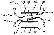
다음에, 본 발명을 광 자기 디스크 장치의 광 헤드에 사용한 다른 실시예를 설명한다. 제 10 도는 광 헤드의 광학계 구성을 도시하는 평면도이고, 제 11 도는 측면도이다. 반도체 레이저 칩(301)은 파장 830nm, 출력 30mW에서 기록용 레이저 빔을 방사한다. 반도체 레이저 칩(302)는 파장 780nm의 저출력 저잡음 레이저 칩에서 재생용 레이저 빔을 방사한다. 2개의 레이저 빔은 조준 렌즈(303)에서 평행 광속으로 되고, 1/2 파장판(304)와 빔 스플리터(305)를 통과하여, 미러(306)에서 반사되어 포커스 렌즈(307)에서 광 자기 디스크(308)의 트랙(309)상에 기록용 스포트(311)과 재생용 스포트(312)로써 조여들어간다. 2개의 스포트(311)과 (312)의 반사 빔은 포커스 렌즈(307)에서 또 다시 평행 광속으로 되어 미러(306)에서 반사되고, 빔 스플리터(305)에서 반사되어 파장 분리 프리즘(313)으로 입사한다. 파장 분리 프리즘(313)은 파장 830nm의 빔을 통과시켜 780nm의 빔을 반사하는 것이다. 따라서, 파장830nm의 기록용 빔은 파장 분리 프리즘(313)을 통과하여, 볼록 렌즈(314), 원주 렌즈(315), 나이프 에지(316) 및 분할형 광 검출기(317)되는 초점 어긋남 검출 및 트랙 어긋남 검출 광학계로 인도된다. 이 검출 광학계의 초점 어긋남 검출 원리나 트랙 어긋남 검출 원리에 대해서는 일본국 특허공개공보 소화57-108811호에 상세하게 기술되어 있다. 한편, 파장 780nm의 재생용 빔은 파장 분리 프리즘(313)에서 반사되어 검광자(318)과 광 검출기(319)로 되는 검광자형 광 자기신호 검출 광학계로 인도된다.Next, another embodiment in which the present invention is used for the optical head of the magneto-optical disk device will be described. 10 is a plan view showing the optical system configuration of the optical head, and FIG. 11 is a side view. The
2개의 반도체 레이저 칩(301)과 (302)는 SiC 세라믹의 서브 마운트(324)와 (329)를 거쳐서 마운트(320)에 탑재되어 있다. 제 12 도는 2개의 반도체 레이저 칩(301),(302)의 탑재 상황을 조준 렌즈(303)측에서 본것으로 서브 마운트(324)와 (329)의 표면에는 패턴 전극이 형성되어 있고, 리이드선(325),(330)에 각각 접속되어 있다. 레이저 칩(301)과 (302)의 전극면(322)와 (327)은 리이드선(323)과 (328)에 각각 접속되어 있다. 전극면(322)와 (327)의 간격은 17㎛이다.Two
레이저 광은 활성층(321)과 (326)에서 각각 방사되어, 활성층(321)과 전극면(322)의 간격은 약 5㎛, 활성층(326)과 전극면(327)의 간격은 약 5㎛이다. 따라서, 2개의 반도체 레이저 칩의 발광점 간격 d는 237㎛이다. 조준 렌즈(303)의 열림 구멍 수 NAc는 0.2, 포커스 렌즈(307)의 열림구멍 수 NAf는 0.53이고, 디스크 상에서 기록용 스포트(311)과 재생용 스포트(312)의 간격 ℓ은 10㎛이다.The laser light is emitted from the
광 디스크(308)의 트랙(309)는 회전에 의해서 편심한다. 트랙 편심량은 통상 최대 약 100μm이다. 이 때문에, 2빔 광 헤드에서는 트랙 어긋남이 생긴다. 이것을 제 13 도를 사용해서 설명한다. 원(331)은 점(332)를 중심으로 하는 반경 a의 트랙으로 한다. 2개의 스포트(333)과 (334)는 ℓ만큼 떨어져서 원(331)의 트랙상에 있다. 다음에, 트랙이 편심한 경우를 생각한다. 예를들면, 트랙이 원(331)의 위치에서 스포트(333)을 중심으로 만큼 회전하여 파선 원(331')로 되었다고 한다. 편심한 트랙의 중심을 점(332'), 또 스포트(334)가 위치하고 있던 트랙상의 점의 새로운 파선 원상의 위치를 점(334')로 표시한다. 점(332)와 점(332')의 간격이 트랙 편심량 W이고, 점(334)와 점(334')의 간격이 트랙 어긋남량 ΔTR이다. 근사적으로The

이기 때문에, 편심량 W에 의해서 생기는 트랙 어긋남량 ΔTR은,Therefore, the track shift amount ΔTR generated by the eccentricity W is

이다. 예를들면, 직경 90mm의 광 디스크의 가장 안쪽 둘레 트랙의 반경은 약 30mm이기 때문에 ℓ=40μm, W=100μm, a=30μm로 하면, 위의 식에서 ΔTR≒0.133μm이다.to be. For example, since the radius of the innermost circumferential track of the optical disk having a diameter of 90 mm is about 30 mm, when L = 40 µm, W = 100 µm, and a = 30 µm, ΔTR ≒ 0.133 µm in the above equation.
그러나, 기록 피트의 중심 위치를 2진화된 기록 데이타의「1」에 대응시키는 피트 센터 기록방식에서는 일반적으로 트랙 어긋남 허용값은 0.13μm 이다. 트랙 어긋남이 0.13μm 이상으로 되면 재생신호의 감소와 인접한 트랙에 기록되어 있는 피트에 의한 누화의 증가에 의해서 재생시의 오율이 증가하여 실용적이 아니다. 트랙 어긋남을 0.13μm 이하로 하기 위해서는 2개의 소프트 간격을 40μm 이하로 할 필요가 있다.However, in the pit center recording method in which the center position of the recording pit corresponds to " 1 " When the track deviation becomes 0.13 µm or more, the error rate during reproduction increases due to the reduction of the reproduction signal and the increase in crosstalk due to the pit recorded in the adjacent track, which is not practical. In order to make track deviation 0.13 micrometers or less, it is necessary to make two
또한, 기록 피트의 에지 위치를 2진화된 기록 데이타의「1」에 대응시키는 피트 에지 기록 방식에서 기록밀도는 2배로 되지만, 트랙 어긋남 허용량은 약 절반인 0.07μm 정도 이하이다. 트랙 어긋남이 0.07μm 이상으로 되면, 재생신호의 위상 어긋남이 크게 되고, 재생시의 오율이 증가하여 실용적이 아니다. 트랙 어긋남을 0.07㎛ 이하로 하기 위해서는 2개의 스포트 간격을 약 20㎛ 이하로 할 필요가 있다. 따라서, 본 실시예의 광 헤드는 피트 센터 기록 방식의 광 자기 디스크에도, 피트 에지 기록방식의 광 자기 디스크에도 사용 할 수가 있다.In addition, in the pit edge recording method in which the edge position of the recording pit corresponds to " 1 " of the binarized recording data, the recording density is doubled, but the track shift allowable amount is about half of 0.07 μm or less. When the track shift becomes 0.07 µm or more, the phase shift of the reproduction signal becomes large, and the error rate during reproduction increases, which is not practical. In order to make the track shift 0.02 micrometers or less, it is necessary to make two spot spaces about 20 micrometers or less. Therefore, the optical head of this embodiment can be used for a pit center recording type magneto-optical disk or a pit edge recording type magneto-optical disk.
광 헤드를 얇게 하는데는 제 10 도와 같이 광학 부품을 1평면내에 배치하는 것이 좋다. 빔 스플리터(305)나 파장 분리 프리즘(313)에서 분리하는 빔도 이 평면내에 포함되는 것이 좋다. 광 이용 효율이나 신호 검출 효율에서 빔 스플리터(305)는 예를들면, P편광 투과율이 약 70%이고, S편광 반사율이 100%의 특성의 것을 사용하여 제 10 도와 같이 디스크에서의 반사빔을 빔 스플리터(305)에서 반사하여 검출 광학계로 인도하는 구성으로 한다. 즉, 반도체 레이저(301),(302)에서의 빔을 P편광으로 해서 빔 스플리터(305)에 입사하면, 투과율 70%의 높은 광 이용 효율이 얻어지고, 디스크에서의 반사 빔에 포함되는 광 자기 신호 성분인 S편광 성분은 효율종게 반사해서 검출 광학계에 도달할 수가 있다. 그러나, 2개의 레이저 칩(301)과 (302)를 대향시킨 경우, 2개의 레이저 칩(301),(302)에서 방사되는 레이저 광의 직선 편광 방향은 제 10 도의 지면과 수직 방향이다. 이것은 빔 스플리터(305)의 S편광 방향이다. 그래서 1/2 파장판(304)를 레이저 칩(301) 및 (302)와 빔 스플리터(305) 사이에 배치하고, 2개의 레이저 빔의 직선 편광 방향을 90도 회전시켜 P편광으로 한다. 1/2 파장판 대신에 예를들면, 패러데이 소자등도 사용할 수 있다.In order to make the optical head thin, it is preferable to arrange the optical component in one plane as in the tenth degree. The beam splitting by the
본 실시예와 같이, 파장이 다른 레이저 칩을 사용하면, 파장 분리 프리즘(313)에 의해서 간단히 2개의 빔을 분리할 수가 있다. 한편, 조준 렌즈(303)이나 포커스 렌즈(307)에는 색수차가 있고, 레이저 칩(301)의 출사 끝면과 레이저 칩(302)의 출사 끝면을 동일 평면에 나란히 하면, 2개의 스포트(311)과 (312)의 초점 위치가 어긋난다. 예를들면, 본 실시예에 사용한 조준 렌즈(303)과 포커스 렌즈(307)을 합친 모든 렌즈계의 색수차는 0.038㎛/nm이고, 50nm의 파장차에 의해 1.9㎛ 어긋난다. 따라서, 이것을 보상하기 위해서, 파장 780nm의 레이저 칩(302)를 파장 830nm의 레이저 칩(301)보다도 광 축에 따라서 조준 렌즈(303) 쪽으로 약 13㎛ 어긋나게 해서 있다.As in the present embodiment, when laser chips having different wavelengths are used, the two beams can be easily separated by the wavelength separation prism 313. On the other hand, there is chromatic aberration in the aiming
본 발명은 상기 실시예에 한정하는 일없이 예를들면, 상변화형의 공 디스크 장치나 추기형 광 디스크 장치 또, 광 카드 장치등에도 사용할 수가 있다.The present invention can be used in, for example, a phase change blank disk device, a recordable optical disk device, an optical card device, and the like without being limited to the above embodiments.
이것에 의해, 광 디스크면 상의 스포트 간격을 최소 40㎛까지 좁게 하는 것이 가능하게 되고, 디스크 편심에 의해서 생기는 트랙 어긋남이 적고, 충분히 실용적인 2빔 광 헤드를 실현할 수가 있다. 또한 2개의 빔 분리가 1개의 광학 소자를 사용하는 것만으로 용이하게 행할 수 있고, 또한 얇은형의 2빔 광 헤드가 가능하게 된다.This makes it possible to narrow the spot distance on the optical disk surface to at least 40 µm, thereby realizing a sufficiently practical two-beam optical head with less track deviation caused by disk eccentricity. Moreover, two beam separation can be performed easily only by using one optical element, and a thin two-beam optical head becomes possible.
상기한 바와같이 본 발명에 의한 반도체 레이저 장치는 여러개의 반도체 레이저 칩으로 되는 반도체 레이저 장치에 있어서, 적어도 한쌍의 레이저 칩이 공간을 두고 서로 마주대하는 2개의 면에 각각 분리해서 고착되어 있는 것 또는 적어도 한쌍의 반도체 레이저 칩의 전극면끼리가 대략 평행 또는 서로 대향하도록 배치되어 있는 것에 의해 여러개의 특성을 달리하는 반도체 레이저 칩의 적재가 가능하게 되고, 그리고도 열적 및 전기적인 간섭을 일으키는 일없이, 상기 반도체 레이저 칩 사이의 발광 스포트 간격을 100㎛ 이하로 좁게 할 수가 있으므로, 예를들면 광 디스크 장치의 소형화, 고속화나 레이저 빔 프린터의 고속화등 반도체 레이저 장치와 그 주변기가 즉, 광 정보 처리 장치의 기능을 향상시킨다는 효과가 있다.As described above, the semiconductor laser device according to the present invention is a semiconductor laser device comprising a plurality of semiconductor laser chips, in which at least one pair of laser chips are separately fixed to two surfaces facing each other with a space therebetween, or at least The electrode faces of a pair of semiconductor laser chips are arranged so as to be substantially parallel or opposite to each other, so that a semiconductor laser chip having various characteristics can be loaded, and without causing thermal and electrical interference, Since the light emission spot spacing between the semiconductor laser chips can be narrowed to 100 μm or less, for example, the functions of the semiconductor laser device and its peripheral devices, such as the miniaturization and speed of the optical disk device and the speed of the laser beam printer, that is, the functions of the optical information processing device. It is effective to improve.
Claims (20)
Translated fromKorean

Applications Claiming Priority (6)
| Application Number | Priority Date | Filing Date | Title |
|---|---|---|---|
| JP62-70268 | 1987-02-26 | ||
| JP62070268AJP2533871B2 (en) | 1987-03-26 | 1987-03-26 | Semiconductor laser device |
| JP87-70268 | 1987-03-26 | ||
| JP87-226339 | 1987-09-11 | ||
| JP62226339AJP2765839B2 (en) | 1987-09-11 | 1987-09-11 | 2-beam optical head |
| JP62-226339 | 1987-09-11 |
Publications (2)
| Publication Number | Publication Date |
|---|---|
| KR880011963A KR880011963A (en) | 1988-10-31 |
| KR910004265B1true KR910004265B1 (en) | 1991-06-25 |
Family
ID=26411434
Family Applications (1)
| Application Number | Title | Priority Date | Filing Date |
|---|---|---|---|
| KR1019880003050AExpiredKR910004265B1 (en) | 1987-03-26 | 1988-03-22 | Semiconductor laser system and manufacture method and light head |
Country Status (2)
| Country | Link |
|---|---|
| US (1) | US4901325A (en) |
| KR (1) | KR910004265B1 (en) |
Families Citing this family (51)
| Publication number | Priority date | Publication date | Assignee | Title |
|---|---|---|---|---|
| JPH0719929B2 (en)* | 1989-03-28 | 1995-03-06 | 三菱電機株式会社 | Semiconductor laser device |
| EP0721753B1 (en)* | 1991-02-20 | 2000-01-26 | Sunrise Medical HHG Inc. | Deformity back system |
| JP2677716B2 (en)* | 1991-03-15 | 1997-11-17 | シャープ株式会社 | Semiconductor laser device |
| US5617441A (en)* | 1991-10-21 | 1997-04-01 | Rohm Co. Ltd. | Light source unit and its manufacturing method, adjusting method and adjusting apparatus |
| JPH05114159A (en)* | 1991-10-22 | 1993-05-07 | Canon Inc | Multibeam optical bead |
| US5293032A (en)* | 1992-02-10 | 1994-03-08 | Sydney Urshan | Digital data optical recording and playback system |
| US5640188A (en)* | 1992-12-18 | 1997-06-17 | Xerox Corporation | Multiple diode laser employing mating substrates |
| US5500768A (en)* | 1993-04-16 | 1996-03-19 | Bruce McCaul | Laser diode/lens assembly |
| US5625189A (en)* | 1993-04-16 | 1997-04-29 | Bruce W. McCaul | Gas spectroscopy |
| US5448071A (en)* | 1993-04-16 | 1995-09-05 | Bruce W. McCaul | Gas spectroscopy |
| US5615052A (en)* | 1993-04-16 | 1997-03-25 | Bruce W. McCaul | Laser diode/lens assembly |
| US5360761A (en)* | 1993-05-07 | 1994-11-01 | Xerox Corporation | Method of fabricating closely spaced dual diode lasers |
| US5324387A (en)* | 1993-05-07 | 1994-06-28 | Xerox Corporation | Method of fabricating asymmetric closely-spaced multiple diode lasers |
| US5521931A (en)* | 1993-11-22 | 1996-05-28 | Xerox Corporation | Nonmonolithic arrays of accurately positioned diode lasers |
| US5576752A (en)* | 1993-11-22 | 1996-11-19 | Xerox Corporation | Offset mounting of nonmonolithic multiwavelength lasers |
| US5355382A (en)* | 1993-11-22 | 1994-10-11 | Xerox Corporation | Composite laser array support |
| US5402436A (en)* | 1993-12-29 | 1995-03-28 | Xerox Corporation | Nonmonolithic array structure of multiple beam diode lasers |
| JPH08111562A (en)* | 1994-10-11 | 1996-04-30 | Mitsubishi Electric Corp | Array-type semiconductor laser device and manufacture thereof |
| US5638393A (en)* | 1994-12-07 | 1997-06-10 | Xerox Corporation | Nonmonolithic multiple laser source arrays |
| JPH0997943A (en)* | 1995-09-28 | 1997-04-08 | Denso Corp | Stucked semiconductor |
| US6205264B1 (en)* | 1998-04-14 | 2001-03-20 | Lucent Technologies Inc. | Optical assembly with improved dimensional stability |
| JP4062648B2 (en)* | 1998-12-25 | 2008-03-19 | シャープ株式会社 | Semiconductor laser and manufacturing method thereof |
| US6819646B1 (en)* | 1999-01-19 | 2004-11-16 | Matsushita Electric Industrial Co., Ltd. | Optical pickup, optical information recording/reproducing apparatus using the same, and phase variable wave plate used in the pickup and the apparatus |
| JP2000223791A (en)* | 1999-02-04 | 2000-08-11 | Sharp Corp | Semiconductor laser device and method of manufacturing the same |
| US6410904B1 (en)* | 1999-11-22 | 2002-06-25 | Brother Kogyo Kabushiki Kaisha | Multi-beam emitting device |
| WO2002065461A2 (en)* | 2001-01-08 | 2002-08-22 | Zen Research (Ireland), Ltd. | Method and apparatus for writing multiple tracks of an optical disk |
| JP4097949B2 (en)* | 2001-04-20 | 2008-06-11 | シャープ株式会社 | Spatial optical transmission system |
| JP2003094716A (en) | 2001-09-20 | 2003-04-03 | Dainippon Screen Mfg Co Ltd | Image recorder and light source unit |
| EP1309048A1 (en)* | 2001-11-06 | 2003-05-07 | Agilent Technologies, Inc. (a Delaware corporation) | Electronic or opto-electronic packages |
| JP2003163405A (en)* | 2001-11-26 | 2003-06-06 | Sony Corp | Double-wavelength semiconductor laser element, astigmatism corrector plate used therefor, and method of arrangement thereof |
| TW200405634A (en)* | 2002-06-03 | 2004-04-01 | Sony Corp | Two-wavelength optical element |
| US7061949B1 (en)* | 2002-08-16 | 2006-06-13 | Jds Uniphase Corporation | Methods, apparatus, and systems with semiconductor laser packaging for high modulation bandwidth |
| US6901086B2 (en)* | 2002-10-30 | 2005-05-31 | Chian Chiu Li | Stack-type diode laser device |
| EP1677397A4 (en)* | 2003-10-24 | 2008-03-19 | Pioneer Corp | Semiconductor laser and manufacturing method |
| CN1839524A (en)* | 2003-12-05 | 2006-09-27 | 日本先锋公司 | Process for fabricating semiconductor laser device |
| JP4466503B2 (en)* | 2005-08-08 | 2010-05-26 | ソニー株式会社 | Semiconductor laser |
| TW200947893A (en)* | 2008-05-08 | 2009-11-16 | Truelight Corp | Dual-wavelength laser element for fiber communication |
| CN101587216B (en)* | 2008-05-20 | 2013-03-20 | 光环科技股份有限公司 | Dual Wavelength Laser Components for Fiber Optic Communications |
| JP5324894B2 (en)* | 2008-11-21 | 2013-10-23 | パナソニック株式会社 | Semiconductor device and manufacturing method thereof |
| JP2010226078A (en)* | 2009-02-24 | 2010-10-07 | Sony Corp | Light-emitting device and method of manufacturing same |
| JP2010199204A (en)* | 2009-02-24 | 2010-09-09 | Sony Corp | Light-emitting device and method of manufacturing the same |
| JP2011014624A (en)* | 2009-06-30 | 2011-01-20 | Sanyo Electric Co Ltd | Method of manufacturing semiconductor laser device, and semiconductor laser device |
| US20130051024A1 (en)* | 2011-08-31 | 2013-02-28 | Moshe Amit | Optical Transmitter Assembly, Optical Transceivers Including the Same, and Methods of Making and Using Such Optical Transmitter Assemblies and Optical Transceivers |
| DE102013224420A1 (en) | 2013-05-13 | 2014-11-13 | Osram Gmbh | Laser component and method for its production |
| US20160036192A1 (en)* | 2014-04-25 | 2016-02-04 | Lasermax, Inc. | Methods for making a laser core |
| US10297975B2 (en) | 2015-10-27 | 2019-05-21 | Mitsubishi Electric Corporation | Laser light source module |
| WO2019205153A1 (en)* | 2018-04-28 | 2019-10-31 | 深圳市大疆创新科技有限公司 | Laser diode packaging module, transmitting apparatus, ranging apparatus, and electronic device |
| CN112074759B (en) | 2018-04-28 | 2024-11-05 | 深圳市大疆创新科技有限公司 | Light detection and ranging sensor with multiple transmitters and multiple receivers and associated systems and methods |
| WO2019205163A1 (en) | 2018-04-28 | 2019-10-31 | SZ DJI Technology Co., Ltd. | Light detection and ranging sensors with multiple emitters and multiple receivers, and associated systems and methods |
| US11714282B2 (en)* | 2019-03-29 | 2023-08-01 | Meta Platforms Technologies, Llc | Compact array light source for scanning display |
| US12000567B2 (en) | 2020-04-15 | 2024-06-04 | Nichia Corporation | Light source device including first substrate supporting first and second laser diodes and second substrate supporting third laser diode |
Family Cites Families (7)
| Publication number | Priority date | Publication date | Assignee | Title |
|---|---|---|---|---|
| GB1040792A (en)* | 1964-02-24 | 1966-09-01 | Nat Res Dev | Optical systems for lasers |
| JPS5946434B2 (en)* | 1978-01-10 | 1984-11-12 | キヤノン株式会社 | semiconductor laser equipment |
| US4477730A (en)* | 1981-04-09 | 1984-10-16 | Fujitsu Limited | Laser apparatus |
| JPS6071289A (en)* | 1983-09-28 | 1985-04-23 | Fuji Photo Film Co Ltd | Thermal recording material |
| US4686678A (en)* | 1984-03-27 | 1987-08-11 | Nec Corporation | Semiconductor laser apparatus with isolator |
| JPS61196446A (en)* | 1985-02-26 | 1986-08-30 | Sony Corp | Photomagnetic recording device |
| JPS61231789A (en)* | 1985-04-08 | 1986-10-16 | Matsushita Electric Ind Co Ltd | Semiconductor laser device |
- 1988
- 1988-03-22KRKR1019880003050Apatent/KR910004265B1/ennot_activeExpired
- 1988-03-25USUS07/173,658patent/US4901325A/ennot_activeExpired - Lifetime
Also Published As
| Publication number | Publication date |
|---|---|
| US4901325A (en) | 1990-02-13 |
| KR880011963A (en) | 1988-10-31 |
Similar Documents
| Publication | Publication Date | Title |
|---|---|---|
| KR910004265B1 (en) | Semiconductor laser system and manufacture method and light head | |
| US5687155A (en) | Optical integrating element and integration type optical pickup device using the same | |
| US6487224B1 (en) | Laser diode assembly | |
| KR100461704B1 (en) | Optical Head | |
| JP2533871B2 (en) | Semiconductor laser device | |
| JP2004325826A (en) | Fixing method and fixed structure of optical member | |
| US20020089913A1 (en) | Light source device for an optical head apparatus and method relating thereto | |
| US20070177488A1 (en) | Optical module and optical recording and/or reproducing apparatus | |
| JP2002094166A (en) | Light source device | |
| JPS58196634A (en) | Light source for optical head | |
| JP2835778B2 (en) | Optical head and its adjustment method | |
| JP2002042365A (en) | Light source device for optical head device | |
| JPH0433550Y2 (en) | ||
| JP2000268387A (en) | Semiconductor light source module manufacturing method and semiconductor light source module | |
| JP3157596B2 (en) | Light head | |
| US20050162994A1 (en) | Two-wavelength optical element | |
| JPH0719376B2 (en) | Light head | |
| JP3518904B2 (en) | Optical pickup | |
| JPH08339570A (en) | Optical head for optical recording and reproducing device | |
| JP2888317B2 (en) | Optical pickup device | |
| JP2004047096A (en) | Optical head for optical recording and reproducing device | |
| Carlin et al. | Durable optical disk system-an update | |
| JPH0765398A (en) | Light emitting and receiving element device | |
| JP2003022556A (en) | Semiconductor laser module and module for integrated optical pickup | |
| JP2002056569A (en) | Optical pickup and information recording / reproducing device |
Legal Events
| Date | Code | Title | Description |
|---|---|---|---|
| A201 | Request for examination | ||
| PA0109 | Patent application | Patent event code:PA01091R01D Comment text:Patent Application Patent event date:19880322 | |
| PA0201 | Request for examination | Patent event code:PA02012R01D Patent event date:19880322 Comment text:Request for Examination of Application | |
| PG1501 | Laying open of application | ||
| E902 | Notification of reason for refusal | ||
| PE0902 | Notice of grounds for rejection | Comment text:Notification of reason for refusal Patent event date:19901130 Patent event code:PE09021S01D | |
| G160 | Decision to publish patent application | ||
| PG1605 | Publication of application before grant of patent | Comment text:Decision on Publication of Application Patent event code:PG16051S01I Patent event date:19910528 | |
| E701 | Decision to grant or registration of patent right | ||
| PE0701 | Decision of registration | Patent event code:PE07011S01D Comment text:Decision to Grant Registration Patent event date:19910917 | |
| GRNT | Written decision to grant | ||
| PR0701 | Registration of establishment | Comment text:Registration of Establishment Patent event date:19910927 Patent event code:PR07011E01D | |
| PR1002 | Payment of registration fee | Payment date:19910927 End annual number:3 Start annual number:1 | |
| PR1001 | Payment of annual fee | Payment date:19940611 Start annual number:4 End annual number:4 | |
| PR1001 | Payment of annual fee | Payment date:19950614 Start annual number:5 End annual number:5 | |
| PR1001 | Payment of annual fee | Payment date:19960620 Start annual number:6 End annual number:6 | |
| PR1001 | Payment of annual fee | Payment date:19970623 Start annual number:7 End annual number:7 | |
| PR1001 | Payment of annual fee | Payment date:19971223 Start annual number:8 End annual number:10 | |
| PR1001 | Payment of annual fee | Payment date:20010612 Start annual number:11 End annual number:11 | |
| PR1001 | Payment of annual fee | Payment date:20020618 Start annual number:12 End annual number:12 | |
| PR1001 | Payment of annual fee | Payment date:20030612 Start annual number:13 End annual number:13 | |
| PR1001 | Payment of annual fee | Payment date:20040607 Start annual number:14 End annual number:14 | |
| PR1001 | Payment of annual fee | Payment date:20050531 Start annual number:15 End annual number:15 | |
| PR1001 | Payment of annual fee | Payment date:20060613 Start annual number:16 End annual number:16 | |
| FPAY | Annual fee payment | Payment date:20070604 Year of fee payment:17 | |
| PR1001 | Payment of annual fee | Payment date:20070604 Start annual number:17 End annual number:17 | |
| EXPY | Expiration of term | ||
| PC1801 | Expiration of term |