KR910001773B1 - Energy focused surface reaction using cluster beams - Google Patents
Energy focused surface reaction using cluster beamsDownload PDFInfo
- Publication number
- KR910001773B1 KR910001773B1KR1019880701310AKR880701310AKR910001773B1KR 910001773 B1KR910001773 B1KR 910001773B1KR 1019880701310 AKR1019880701310 AKR 1019880701310AKR 880701310 AKR880701310 AKR 880701310AKR 910001773 B1KR910001773 B1KR 910001773B1
- Authority
- KR
- South Korea
- Prior art keywords
- clusters
- cluster
- reactant
- energy
- reaction
- Prior art date
- Legal status (The legal status is an assumption and is not a legal conclusion. Google has not performed a legal analysis and makes no representation as to the accuracy of the status listed.)
- Expired
Links
Images


Classifications
- C—CHEMISTRY; METALLURGY
- C23—COATING METALLIC MATERIAL; COATING MATERIAL WITH METALLIC MATERIAL; CHEMICAL SURFACE TREATMENT; DIFFUSION TREATMENT OF METALLIC MATERIAL; COATING BY VACUUM EVAPORATION, BY SPUTTERING, BY ION IMPLANTATION OR BY CHEMICAL VAPOUR DEPOSITION, IN GENERAL; INHIBITING CORROSION OF METALLIC MATERIAL OR INCRUSTATION IN GENERAL
- C23C—COATING METALLIC MATERIAL; COATING MATERIAL WITH METALLIC MATERIAL; SURFACE TREATMENT OF METALLIC MATERIAL BY DIFFUSION INTO THE SURFACE, BY CHEMICAL CONVERSION OR SUBSTITUTION; COATING BY VACUUM EVAPORATION, BY SPUTTERING, BY ION IMPLANTATION OR BY CHEMICAL VAPOUR DEPOSITION, IN GENERAL
- C23C14/00—Coating by vacuum evaporation, by sputtering or by ion implantation of the coating forming material
- C23C14/22—Coating by vacuum evaporation, by sputtering or by ion implantation of the coating forming material characterised by the process of coating
- C23C14/24—Vacuum evaporation
- C23C14/32—Vacuum evaporation by explosion; by evaporation and subsequent ionisation of the vapours, e.g. ion-plating
- C—CHEMISTRY; METALLURGY
- C23—COATING METALLIC MATERIAL; COATING MATERIAL WITH METALLIC MATERIAL; CHEMICAL SURFACE TREATMENT; DIFFUSION TREATMENT OF METALLIC MATERIAL; COATING BY VACUUM EVAPORATION, BY SPUTTERING, BY ION IMPLANTATION OR BY CHEMICAL VAPOUR DEPOSITION, IN GENERAL; INHIBITING CORROSION OF METALLIC MATERIAL OR INCRUSTATION IN GENERAL
- C23C—COATING METALLIC MATERIAL; COATING MATERIAL WITH METALLIC MATERIAL; SURFACE TREATMENT OF METALLIC MATERIAL BY DIFFUSION INTO THE SURFACE, BY CHEMICAL CONVERSION OR SUBSTITUTION; COATING BY VACUUM EVAPORATION, BY SPUTTERING, BY ION IMPLANTATION OR BY CHEMICAL VAPOUR DEPOSITION, IN GENERAL
- C23C14/00—Coating by vacuum evaporation, by sputtering or by ion implantation of the coating forming material
- C23C14/22—Coating by vacuum evaporation, by sputtering or by ion implantation of the coating forming material characterised by the process of coating
- C23C14/221—Ion beam deposition
- H—ELECTRICITY
- H01—ELECTRIC ELEMENTS
- H01L—SEMICONDUCTOR DEVICES NOT COVERED BY CLASS H10
- H01L21/00—Processes or apparatus adapted for the manufacture or treatment of semiconductor or solid state devices or of parts thereof
- H01L21/02—Manufacture or treatment of semiconductor devices or of parts thereof
- H01L21/04—Manufacture or treatment of semiconductor devices or of parts thereof the devices having potential barriers, e.g. a PN junction, depletion layer or carrier concentration layer
- H01L21/18—Manufacture or treatment of semiconductor devices or of parts thereof the devices having potential barriers, e.g. a PN junction, depletion layer or carrier concentration layer the devices having semiconductor bodies comprising elements of Group IV of the Periodic Table or AIIIBV compounds with or without impurities, e.g. doping materials
- H01L21/28—Manufacture of electrodes on semiconductor bodies using processes or apparatus not provided for in groups H01L21/20 - H01L21/268
- H01L21/283—Deposition of conductive or insulating materials for electrodes conducting electric current
- H01L21/285—Deposition of conductive or insulating materials for electrodes conducting electric current from a gas or vapour, e.g. condensation
- H01L21/28506—Deposition of conductive or insulating materials for electrodes conducting electric current from a gas or vapour, e.g. condensation of conductive layers
- H01L21/28512—Deposition of conductive or insulating materials for electrodes conducting electric current from a gas or vapour, e.g. condensation of conductive layers on semiconductor bodies comprising elements of Group IV of the Periodic Table
- H01L21/28518—Deposition of conductive or insulating materials for electrodes conducting electric current from a gas or vapour, e.g. condensation of conductive layers on semiconductor bodies comprising elements of Group IV of the Periodic Table the conductive layers comprising silicides
- H—ELECTRICITY
- H01—ELECTRIC ELEMENTS
- H01L—SEMICONDUCTOR DEVICES NOT COVERED BY CLASS H10
- H01L21/00—Processes or apparatus adapted for the manufacture or treatment of semiconductor or solid state devices or of parts thereof
- H01L21/02—Manufacture or treatment of semiconductor devices or of parts thereof
- H01L21/04—Manufacture or treatment of semiconductor devices or of parts thereof the devices having potential barriers, e.g. a PN junction, depletion layer or carrier concentration layer
- H01L21/18—Manufacture or treatment of semiconductor devices or of parts thereof the devices having potential barriers, e.g. a PN junction, depletion layer or carrier concentration layer the devices having semiconductor bodies comprising elements of Group IV of the Periodic Table or AIIIBV compounds with or without impurities, e.g. doping materials
- H01L21/30—Treatment of semiconductor bodies using processes or apparatus not provided for in groups H01L21/20 - H01L21/26
- H01L21/302—Treatment of semiconductor bodies using processes or apparatus not provided for in groups H01L21/20 - H01L21/26 to change their surface-physical characteristics or shape, e.g. etching, polishing, cutting
- H01L21/306—Chemical or electrical treatment, e.g. electrolytic etching
- H01L21/3065—Plasma etching; Reactive-ion etching
- H—ELECTRICITY
- H01—ELECTRIC ELEMENTS
- H01J—ELECTRIC DISCHARGE TUBES OR DISCHARGE LAMPS
- H01J2237/00—Discharge tubes exposing object to beam, e.g. for analysis treatment, etching, imaging
- H01J2237/06—Sources
- H01J2237/08—Ion sources
- H01J2237/0812—Ionized cluster beam [ICB] sources
- Y—GENERAL TAGGING OF NEW TECHNOLOGICAL DEVELOPMENTS; GENERAL TAGGING OF CROSS-SECTIONAL TECHNOLOGIES SPANNING OVER SEVERAL SECTIONS OF THE IPC; TECHNICAL SUBJECTS COVERED BY FORMER USPC CROSS-REFERENCE ART COLLECTIONS [XRACs] AND DIGESTS
- Y10—TECHNICAL SUBJECTS COVERED BY FORMER USPC
- Y10S—TECHNICAL SUBJECTS COVERED BY FORMER USPC CROSS-REFERENCE ART COLLECTIONS [XRACs] AND DIGESTS
- Y10S438/00—Semiconductor device manufacturing: process
- Y10S438/961—Ion beam source and generation
Landscapes
- Engineering & Computer Science (AREA)
- Chemical & Material Sciences (AREA)
- Physics & Mathematics (AREA)
- General Physics & Mathematics (AREA)
- Power Engineering (AREA)
- Microelectronics & Electronic Packaging (AREA)
- Computer Hardware Design (AREA)
- Manufacturing & Machinery (AREA)
- Condensed Matter Physics & Semiconductors (AREA)
- Metallurgy (AREA)
- Organic Chemistry (AREA)
- Mechanical Engineering (AREA)
- Materials Engineering (AREA)
- Chemical Kinetics & Catalysis (AREA)
- Plasma & Fusion (AREA)
- Physical Or Chemical Processes And Apparatus (AREA)
- ing And Chemical Polishing (AREA)
- Physical Vapour Deposition (AREA)
- Chemical Vapour Deposition (AREA)
- Physical Deposition Of Substances That Are Components Of Semiconductor Devices (AREA)
- Drying Of Semiconductors (AREA)
Abstract
Translated fromKoreanDescription
Translated fromKorean제1도는 단일 클러스터 비임을 제조하는 클러스터 비임 증착 장치의 개략적인 설명도이고,1 is a schematic illustration of a cluster beam deposition apparatus for producing a single cluster beam,
제2도는 2개의 클러스터 비임을 제조하는 클러스터 비임 증착 장치의 개략적인 설명도이며,2 is a schematic illustration of a cluster beam deposition apparatus for manufacturing two cluster beams,
제3도는 클러스터 공급원의 일측 단면도이고,3 is a cross-sectional side view of a cluster source,
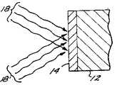
제4도는 에너지가 가해진 에칭 반응을 설명하는 것으로서, 기판 및 그 표면의 일측 단면도이며,4 is a cross-sectional view of one side of the substrate and its surface, illustrating an energy-etched etching reaction,
제5도는 에너지가 가해진 피막 증착 반응을 설정하는 것으로서, 기판 및 그 표면의 일측 단면도이고,5 is a cross sectional view of one side of the substrate and its surface, which sets up an energy-induced film deposition reaction,
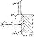
제6도는 외부에서 도입된 2가지 반응물을 사용하고 에너지가 가해진 피막 증착 반응을 설명하는 것으로서, 기판 및 그 표면의 일측 단면도이며,6 is a cross-sectional view of one side of the substrate and its surface, illustrating an energized film deposition reaction using two externally introduced reactants,
제7도는 반응물 및 에너지를 공급하는 2개의 클러스터 비임을 사용하는 에너지가 가해진 피막 증착 반응을 설명하는 것으로서, 기판 및 그 표면의 일측 단면도이다.FIG. 7 illustrates an energized film deposition reaction using a reactant and two cluster beams to supply energy, and is a cross-sectional side view of the substrate and its surface.
본 발명은 표면에 에너지를 집중(intensive)시키는 화학 반응, 더욱 구체적으로는 표면 반응에 있어서 반응물과 에너지가 모두 외부에서 공급되는 표면 화학 반응에 관한 것이다.The present invention relates to a chemical reaction that concentrates energy on a surface, and more particularly to a surface chemical reaction in which both reactants and energy are supplied from the outside in the surface reaction.
표면에서는 여러 가지 유형의 화학 반응이 일어나거나 진행될 수 있다. 대부분의 접촉 반응 및 반응물이 외부원으로부터 공급되는 반응의 생성물로서 얻어지는 피막의 증착(deposition)과 같은 일부반응에 있어서, 표면은 반응이 일어날 수 있는 반응 영역은 제공하지만, 그 자체가 화학 반응물이 되지는 않는다. 다른 반응, 예컨대 표면의 에칭 또는 원자나 분자를 포함하는 표면 반응에 의해 형성된 반응 생성물로서의 피막의 성장과 같은 반응에서는 표면 그 자체가 하나의 반응물을 제공함으로써 반응에 관여한다.Various types of chemical reactions can occur or progress on the surface. In some reactions, such as the deposition of a coating, in which most contact reactions and reactants are obtained as a product of a reaction supplied from an external source, the surface provides a reaction zone where the reaction can occur, but does not itself become a chemical reactant. Does not. In other reactions, such as the growth of a coating as a reaction product formed by etching of a surface or surface reaction involving atoms or molecules, the surface itself is involved in the reaction by providing one reactant.
많은 표면 반응은 산업상 대단히 중요하거나 중요한 것일 수 있다. 접촉 반응은 화학 제품을 생산하기 위해 널리 사용된다. 피막의 일부가 반응하여 제거되는 화학적인 처리 방법인 피막의 화학적인 에칭은 미소 전자 가공 기술의 주요한 특징이다. 화학 증착법에서와 같이 표면에서의 피막의 반응성 증착은 다른 방법으로는 제조될 수 없는 전자 및 광학적인 응용을 위한 특수한 유형의 피막 제조를 가능하게 해준다.Many surface reactions can be very important or important in industry. Contact reactions are widely used to produce chemicals. Chemical etching of the coating, a chemical treatment method in which part of the coating reacts and is removed, is a major feature of the microelectronic processing technology. As in chemical vapor deposition, reactive deposition of the coating on the surface allows for the production of special types of coatings for electronic and optical applications that cannot be produced by other methods.
표면에서 일어나는 많은 반응들은 반응 에너지 장벽을 넘기위해 에너지의 투입을 필요로 한다. 대부분의 화학 반응들은 반응물에 에너지를 가했을 때 촉진되며, 보다 빠른 화학 반응은 표면 반응 이용의 경제성을 개선한다. 대부분의 통상적인 에너지 제공 방법은 지지 기판을 통해 표면을 가열함으로써 표면의 반응물에 에너지를 제공한다. 이 방법은, 반응 생성물로서 피막을 증착시키는데 응용될 경우, 이미 증착된 층도 함께 가열하게 되는 단점이 있다. 이와 같이 이미 증착된 층이 가열되면 바람직하지 못한 층간 확산이 일어날 수 있으며, 이렇게 될 경우 서로 다른 층들이 서로의 상부에 증착된다.Many reactions that take place on the surface require the input of energy to cross the reactive energy barrier. Most chemical reactions are accelerated by energizing the reactants, and faster chemical reactions improve the economics of using surface reactions. Most conventional energy provision methods provide energy to the reactants on the surface by heating the surface through a support substrate. This method has the disadvantage that when applied to deposit a coating as a reaction product, the already deposited layer is also heated together. Undesired interdiffusion can occur when the already deposited layer is heated, in which case different layers are deposited on top of each other.
표면에서 일어나는 반응에 에너지를 제공하기 위한 또다른 방법은 레이저 광선이나 자외선 광선 등을 사용하여 표면에 에너지를 집중시키는 방법이다. 이 방법은 부분적으로 성공적이었으나, 투사광을 적당히 조정하여 그 에너지가 반응물의 에너지와 결함되도록 집중시켜야 한다. 집중되는 광은 고에너지 준위를 전달하기 위해 가능한한 강해야 하지만. 그 강도는 표면에 열을 전달하는 것만으로 제한되는 것이 바람직하다. 열의 일부는 기판의 냉각에 의해 제거될 수 있지만, 표면층의 의도하지 않은 가열 및 용융은 표면 반응 중에 도입될 수 있는 동력의 한가지 제한 요인이 된다. 표면에 에너지를 제공하기 위한 또다른 방법은 표면에 플라즈마를 발생시키는 방법이다. 그러나, 플라즈마장(場)은 종종 표면에 추가의 반응물을 운반하는 능력을 제한하고, 투입 에너지량을 조절하기 어려우므로 표면에 바람직하지 못한 부작용을 일으킬 수 있다.Another way to provide energy for reactions on the surface is to concentrate energy on the surface using laser or ultraviolet light. This method has been partially successful, but requires the proper adjustment of the projected light so that its energy is concentrated with the energy of the reactants. The focused light should be as strong as possible to deliver high energy levels. Its strength is preferably limited to only transferring heat to the surface. Some of the heat can be removed by cooling the substrate, but unintentional heating and melting of the surface layer is one limiting factor of the power that can be introduced during the surface reaction. Another method for providing energy to the surface is to generate a plasma on the surface. However, plasma fields often limit the ability to carry additional reactants to the surface and are difficult to control the amount of energy input, which can cause undesirable side effects on the surface.
따라서, 표면 반응의 이용이 양호하게 확정되고, 산업상 널리 사용되며, 적어도 몇가지 유형의 반응에 에너지를 제공해야 한다는 필요성은 인식하고 있지만, 반응의 진행에 따라 표면에 반응물과 에너지를 동시에 도입하는 데에는 여전히 어려움이 따른다. 따라서, 표면에 조절 가능한 방식으로 반응물과 에너지를 함께 제공할 수 있는 기술의 필요성이 있게 된다. 본 발명은 이러한 필요성을 이행하고, 추가로 이와 관련된 잇점들을 제공한다.Thus, while the use of surface reactions is well established, widely used industrially, and recognized the need to provide energy for at least some types of reactions, it is important to simultaneously introduce reactants and energy to the surface as the reaction proceeds. Still difficult. Thus, there is a need for a technique that can provide reactants and energy together in an adjustable manner on the surface. The present invention fulfills this need and further provides advantages in this regard.
발명의 요약Summary of the Invention
본 발명은 표면 반응에 반응물과 에너지를 양호하게 조절된 방식으로 동시에 도입하는 기술에 관한 것이다. 에너지는, 표면에 도입되기 전에, 외부에서 도입되는 반응종(反應種)에 직접 조절 가능한 방식으로 가해진다. 반응종의 첨가는 표면에 인접한 공간 전하에 의해 제한되지 않는다. 이 방법은 매우 가변적이며, 에칭, 피막 증착 및 접촉 반응과 같은 여러가지 유형의 표면 반응에 사용될 수 있다. 기판 표면은 반응물의 강력한 도입에 의해 손싱되지 않는다. 이 방법은 또한 표면의 불순물을 연속적으로 청소하고, 표면 결함을 감소 내지는 제거한다.The present invention is directed to a technique for simultaneously introducing reactants and energy into a surface reaction in a well controlled manner. Energy is applied in a directly adjustable manner to the reactive species introduced from the outside before being introduced to the surface. The addition of reactive species is not limited by the space charge adjacent to the surface. This method is very variable and can be used for various types of surface reactions, such as etching, film deposition, and contact reactions. The substrate surface is not compromised by the strong introduction of reactants. The method also continuously cleans the surface of impurities and reduces or eliminates surface defects.
본 발명에 의하면, 외부에서 에너지를 얻는 표면 화학 반응의 수행 방법은 휘발성 반응종을 2 내지 약10.000 단위 함유하는 클러스터(cluster)을 형성하는 단계, 이 클러스터를 표면을 향해 가속하는 단계 및 클러스터를 표면에 충돌시킴으로써 클러스터가 붕해되어 표면 화학 반응에 반응물과 에너지를 공급하는 단계로 이루어진다.According to the present invention, a method of performing a surface chemical reaction for obtaining energy from the outside may include forming a cluster containing 2 to about 10,000 units of volatile reactive species, accelerating the cluster toward the surface, and surface the cluster. This impinges upon the clusters disintegrating and supplying reactants and energy to the surface chemical reaction.
본 명세서에 사용된 바와 같이, 클러스터는 구성 단위들이 약하게 결합한 접합체로서, 전형적으로 클러스터의 균일 또는 불균일 핵생성을 이용하여 농축시킴으로써 형성된다. "단위 (units)"는 클러스터 중에서 각기 독립적으로 존재하지만, 이하 논의되는 이유로 해서 클러스터로 형성되는 원자, 분자 또는 착물이 될 수 있다. 클러스터는 전자 충격에 의해 이온화되지만, 바람직하기로는 하나가 이온화되거나, 또는 많아야 수개의 이온 하전을 띄도록 약하게 이온화되는 것이 좋다. 즉, 각 클러스터의 단위들이 개별적으로 이온화되는 것이 아니라, 전체 클러스터로부터 단지 한개 내지는 수개의 전자가 제거된다. 클러스터는 전기장과 이온화된 클러스터의 반응에 의해 발생되는 가속 전위에 의해 기판을 향해 가속된다. 전형적으로, 클러스터는 구성 단위 한개 질량의 1000배나 되는 큰 질량을 갖기 때문에, 생성된 클러스터 비임은 그 자체 내의 공간 하전에 의해 분산되지 않는다As used herein, clusters are conjugates in which the structural units are weakly bonded, typically formed by concentrating using the homogeneous or heterogeneous nucleation of the clusters. "Units" are each independently present in a cluster, but may be atoms, molecules or complexes formed into clusters for the reasons discussed below. The clusters are ionized by electron bombardment, but preferably one is ionized or weakly ionized to at most several ionic charges. That is, the units of each cluster are not ionized individually, but only one or several electrons are removed from the entire cluster. The cluster is accelerated towards the substrate by an acceleration potential generated by the reaction of the electric field with the ionized cluster. Typically, because the cluster has a mass as large as 1000 times the mass of one structural unit, the resulting cluster beam is not dispersed by the space charge in itself.
클러스터가 표적 기판의 표면에 충돌했을때, 클러스터는 즉시 클러스터를 이루는 개개의 단위들로 붕해된다. 각 단위들은 클러스터 전체 에너지를 클러스터 중의 전체 단위 수로 나눈 것과 같은 작은 에너지를 갖기 때문에, 표면에 거의 손상을 주지 않고, 결함이 거의 생기지 않는다. 클러스터 단위들은 표면 위의 오염물질을 제거하기에 충분한 에너지를 갖기 때문에, 증착과 동시에 표면을 청소한다. 클러스터의 붕해에 의해 생성된 단위들은 또한 표면 위의 다른 반응들이나 반응종에 에너지를 주어 이동하거나 반응하기에 충분한에너지를 갖게 한다. 피막이 증착되고 있는 경우, 반응종과 비반응종들의 이동은 표면을 본 방법에 필요한 온도보다 훨씬 더 높은 온도로 가열했을 경우와 동일한 결과를 제공함과 동시에 증착된 피막의 균일성을 증가시킨다. 그러나, 이미 증착된 층들은 가열되지 않기 때문에, 이미 증착되어 내부에 매립된 구조는 변화되지 않는다.When the cluster impinges on the surface of the target substrate, the cluster immediately disintegrates into individual units that make up the cluster. Since each unit has a small energy such as the total energy of the cluster divided by the total number of units in the cluster, it hardly damages the surface and hardly causes defects. Since the cluster units have enough energy to remove contaminants on the surface, the surface is cleaned simultaneously with deposition. The units produced by the disintegration of the clusters also energize other reactions or reactive species on the surface to have enough energy to move or react. When the coating is being deposited, the migration of reactive and non-reactive species gives the same results as heating the surface to a temperature much higher than the temperature required for the method, while increasing the uniformity of the deposited film. However, since the already deposited layers are not heated, the structure already deposited and embedded therein does not change.
클러스터를 형성하는 단위들에 의해 공급되는 반응물은 표면에서의 반응이 요구하는데 따라 여러가지 종류의 것이 될 수 있다. 예를 들면, 표면 반응은 표면의 에칭이 될 수 있고, 이 경우 에칭제가 클러스터의 반응종 단위로서 제공된다. 이 실시 태양에 의하면, 표면의 에칭 방법은, 각 클러스터마다 휘발성의 반응성 에칭제종을 함유하는 단위들을 2 내지 약 10,000개 함유하는 클러스터들을 형성하는 단계, 이러한 클러스터를 이온화하는 단계, 그 클러스터를 표면을 향해 가속시키는 단계 및 상기 클러스터를 표면에 충돌시킴으로써 클러스터가 붕해되어 에칭제종과 에너지를 표면에서의 에칭 반응에 제공하는 단계로 이루어진다.The reactants supplied by the units forming the cluster can be of various kinds depending on the reaction required at the surface. For example, the surface reaction may be an etching of the surface, in which case the etchant is provided as a reactive species unit of the cluster. According to this embodiment, the method of etching a surface comprises forming clusters containing from 2 to about 10,000 units containing volatile reactive etchant species for each cluster, ionizing such clusters, Accelerating towards the surface and impinging the cluster on the surface to provide etchant species and energy to the etching reaction on the surface.
통상의 방법으로 에칭되거나 또는 특정한 방식으로 에칭시켜야 하는 반도체 재료에 사용하기에 바람직한 형태의 에칭제는 해리하여 할로겐을 유리시키거나 또는 에너지화된 표면 환경내에서 화학적으로 반응성으로되는 할로겐을 함유하는 분자들이다. 이와 같은단위로는 CCl4, CF4및 NF3가 있다. 이 단위들은 클러스터를 형성하는데, 형성된 클러스터는 이온화되어 실리콘과 같은 전형적인 반도체 표면을 향해 가속된다. 충돌시 에너지를 얻은 단위들은 해리하여 유리 할로겐을 생성하고, 이 유리 할로겐은 표면 원자와 반응한다. 반응 생성물은 휘발성이며, 에칭된 재료는 가스상 염화물이나 불화물 행태로서 표면을 이탈한다. 클러스터 비임은 일반적으로 표면에 대해서 집중되어 일반적인 에칭 청소를 달성하거나, 또는 조절된 방식으로 집중되어 표면중에 대응하는 패턴 선택적으로 에칭할 수 있다.Etching agents of the preferred form for use in semiconductor materials that are etched in a conventional manner or must be etched in a particular manner dissociate to release halogens or molecules containing halogens that are chemically reactive within an energized surface environment. admit. Such units include CCl4 , CF4 and NF3 . These units form clusters, which are ionized to accelerate towards a typical semiconductor surface, such as silicon. The energy units in the collision dissociate to produce free halogens, which react with surface atoms. The reaction product is volatile and the etched material leaves the surface as a gaseous chloride or fluoride behavior. The cluster beams may generally be concentrated to the surface to achieve general etch cleaning, or may be concentrated in a controlled manner to selectively etch the corresponding pattern in the surface.
본 발명의 또다른 응용에 의하면, 반응 생성물의 피막을 표면위에 증착시킬 수 있다. 이러한 피막은 클러스터 반응물과 기판 사이의 반응에 의해 생성된 안정한 단일 반응층을 구성할 수 있다. 예를 들면, 질화실리콘 층을 실리콘 기판의 표면에 만들고자 하는 경우, 휘발성의 반응성 질소 함유 단위를 클러스터 형태로 형성하여 표면에 대해서 집중시킴으로써 수행할 수 있다. 이와 같은 경우에, 피막은 확산 운동이 본질적으로 기판 재료 반응물의 공급을 중단시킬 때까지 두꺼워져, 더 이상 성장하지 않게 된다. 표면에 공급되는 모든 반응 생성물이 외부에서 공급되고, 적어도 일부가 에너지를 얻은 클러스터에 의해 공급될 때, 반응 생성물은 또한 임의로 두꺼운 층으로 형성된 피막을 구성할 수 있다. 일례로서, 임의의 두께를 갖는 텅스텐피막은 표면에 대해서 W(CO)6와 같은 텅스텐을 함유하는 화합물의 클러스터를 집중시킴으로써 성장시킬수 있다. 클러스터는 에너지를 얻어 분해되어 표면에 텅스텐을 증착시키고, 휘발성의 일산화탄소종이 표면으로부터 빠져나간다. 본 발명의 또 다른 형태에서는, 다른 반응종을 표면의 외부로부터 제공할 수 있기 때문에, 클러스터 반응종 및 다를 반응종은 표면에서 에너지화 된 상태의 반응물이 될 것이다. 일례로, 표면에 AsH3클러스터와 테트라메틸갈륨이 함께 증착되고 휘발성 수소 및 에탄종이 유리된 후 표면을 이탈함과 동시에 비소화갈륨 피막을 형성한다.According to another application of the invention, a coating of the reaction product can be deposited on the surface. Such coatings may constitute a stable single reaction layer produced by the reaction between the cluster reactant and the substrate. For example, when a silicon nitride layer is to be made on the surface of a silicon substrate, it can be performed by forming volatile reactive nitrogen containing units in cluster form and concentrating on the surface. In such a case, the coating is thickened until the diffusion motion essentially stops the supply of the substrate material reactant and no longer grows. When all reaction products supplied to the surface are supplied externally and at least a part is supplied by the energized clusters, the reaction products may also constitute a film formed of an arbitrarily thick layer. As an example, a tungsten coating having any thickness can be grown by concentrating a cluster of tungsten containing compounds such as W (CO)6 on the surface. The cluster gets energy to decompose to deposit tungsten on the surface, and volatile carbon monoxide species escape from the surface. In another embodiment of the present invention, since other reactive species can be provided from the outside of the surface, the cluster reactive species and the other reactive species will be reactants in the energized state at the surface. In one example, AsH3 clusters and tetramethylgallium are deposited together on the surface and volatile hydrogen and ethane species are released, leaving the surface and simultaneously forming a gallium arsenide film.
이 방법에 의하면, 표면위에 반응 피막을 형성하는 방법은 피막으로 증착되는 휘발성 반응종의 단위들을 각 클러스터 마다 2 내지 약 10,000개 함유하는 클러스터를 형성하는 단계, 클러스터를 이온화하는 단계, 클러스터를 표면을 향해 가속시키는 단계 및 클러스터를 표면에 충돌시킴으로써 클러스터가 분해되어 표면에서의 증착 반응에 반응종과 에너지를 제공하는 단계로 이루어지며, 클러스터로부터 제공된 반응종을 포함하는 화학 반응의 결과로서 상기 피막이 형성된다. 이 반응은 클러스터에 의해 제공된 단일 반응물을 포함할 수 있다. 이 반응은 또한 표면 자체 또는 다른 외부 공급원에 의해 제공되는 다수의 반응종을 포함할 수 있다.According to this method, a method of forming a reactive film on a surface comprises forming a cluster containing 2 to about 10,000 units of each volatile reactive species deposited into the film, ionizing the cluster, and clustering the surface of the cluster. Accelerating towards the surface and impinging the cluster onto the surface to decompose the cluster to provide reactive species and energy to the deposition reaction on the surface, the coating being formed as a result of a chemical reaction comprising the reactive species provided from the cluster. . This reaction may comprise a single reactant provided by the cluster. This reaction may also include a number of reactive species provided by the surface itself or other external sources.
본 발명의 또 다른 별법은 각각 반응종을 공급하는 2이상의 클러스터 형태를 표면에 집중시킬 수 있는 방법이다. 이 방법은 반응이 진행하는데 고준위의 에너지를 필요로 하는 경우에 특히 유용한데, 그 이유는 각 반응물 단위가 고준위의 에너지를 운반하기 때문이다. 이 실시 태양에 의하면, 외부로부터 에너지를 얻어 표면에서의 화학 반응을 달성하는 방법은 휘발성 반응종을 2 내지 약 10,000단위 함유하는 제 1클러스터를 형성하는 단계, 제 1클러스터를 이온화하는 단계, 제 1클러스터를 표면을 향해 가속시키는 단계, 제 1클러스터를 표면상에 충돌시킴으로써 제 1클러스터를 붕해시켜 제 1반응물 및 에너지를 표면에서의 화학 반응에 제공하는 단계, 제 2반응종을 함유하는 단위를 2 내지 약 10,000개 함유하는 제 2클러스터를 형성하는 단계, 제 2클러스터를 이온화하는 단계, 제 2 클러스터를 표면을 향해 가속시키는 단계 및 제 2클러스터를 표면에 충돌시킴으로써 제 2클러스터를 붕해해서 제 2반응물 및 에너지를 표면에서의 화학 반응에 제공하는 단계로 이루어진다. 전형적으로, 제1 및 제2유형의 클러스터들은 본질적으로 동시에 표면에 제공되거나, 또는 일정 간격으로 계속해서 적당한 비율로 제공되어, 목적하는 화학 반응을 소정의 화학양론적인 반응으로 되도록한다. 클러스터 공급원의 하나 또는 양쪽 모두가 펄스되는 경우에도 에너지를 얻은 반응종들은 전형적으로 반응이 일어날 수 있는 충분히 긴 시간 동안 표면위에 체류하게 되는데 이런 의미에서 그 클러스터 공급원들은 동시에 작용한다고 볼 수 있다.Another alternative of the present invention is a method in which two or more cluster forms, each supplying reactive species, can be concentrated on the surface. This method is particularly useful when the reaction requires a high level of energy, because each reactant unit carries a high level of energy. According to this embodiment, a method of obtaining energy from the outside to achieve a chemical reaction on a surface comprises forming a first cluster containing 2 to about 10,000 units of volatile reactive species, ionizing the first cluster, Accelerating the cluster toward the surface, disintegrating the first cluster by impinging the first cluster on the surface to provide the first reactant and energy to the chemical reaction at the surface, and the unit containing the second reactive species. Forming a second cluster containing from about 10,000 to about 10,000, ionizing the second cluster, accelerating the second cluster towards the surface, and disintegrating the second cluster by impinging the second cluster against the surface to react the second reactant. And providing energy to the chemical reaction at the surface. Typically, clusters of the first and second types are provided on the surface at essentially the same time, or continuously at appropriate intervals in suitable proportions, such that the desired chemical reaction is brought into the desired stoichiometric reaction. Even if one or both of the cluster sources are pulsed, the energized reactive species typically stay on the surface for a long enough time for the reaction to occur, in which sense the cluster sources act simultaneously.
비휘발성 물질로 된 클러스터를 형성하지 않은 반응성 가스와 동시에 표면에 대해서 집중시킴으로써 반응 피막을 증착시키는 방법은 이미 공지되어 있다. 휘발성 반응종의 단위들로 된 클러스터를 형성하는 본 방법은 상기 방법에 비해 주요한 기술적인 잇점과 상업적인 잇점을 갖는다(본 명세서 및 당 업계에서 사용되는 "휘발성" 물질은 실온 또는 약간 높은 온도에서 가스를 형성하는 반면에, "비휘발성" 물질은 실온 또는 약간 높은 온도에서 고체이기 때문에, 그의 증기 분압을 얻기 위해서는 고온으로 가열해야만 한다). 비휘발성 물질의 클러스터 형성 효율은 수 퍼센트 정도로 작다. 즉, 전형적인 크기의 장치에서 1초당 단지 1012내지 1013개의 클러스터가 형성된다. 휘발성 물질의 클러스터 형성 효율은 75% 이상으로 훨씬 높은 경우도 있다. 즉, 비교 장치에서 1초당 1015내지 1016개의 클러스터가 형성된다. 따라서, 본 방법은 비휘발성의 클러스터 물질을 사용하는 경우보다 여러 배 더 높은 클러스터 흐름을 제공한다. 따라서, 휘발성 클러스터를 사용할 경우, 대규모의 공업적인 실시가 가능하다.It is already known to deposit a reaction film by concentrating on the surface simultaneously with a reactive gas which does not form a cluster of nonvolatile materials. The method of forming clusters of units of volatile reactive species has major technical and commercial advantages over the method (the "volatile" materials used herein and in the art are characterized by gas at room temperature or slightly higher temperature). On the other hand, since the "non-volatile" material is solid at room temperature or slightly higher temperature, it must be heated to high temperature to obtain its vapor partial pressure). Cluster formation efficiency of nonvolatile materials is as small as a few percent. That is, in a typical sized device only 1012 to 1013 clusters are formed per second. The efficiency of cluster formation of volatiles is often much higher than 75%. That is, 1015 to 1016 clusters are formed per second in the comparison apparatus. Thus, the method provides many times higher cluster flow than with nonvolatile cluster materials. Therefore, when using a volatile cluster, large scale industrial implementation is possible.
본 발명의 방법은 반응물 및 에너지 모두를 클러스터 형태로 표면에 제공함으로써 당업계의 표면 화학 반응에 있어서 중요한 발전을 제공한다는 사실을 알 수 있을 것이다. 피막 증착이 처리 공정의 목적인 경우, 또 다른 중요한 잇점은 표면 청소와, 균일하고, 극히 완벽하고도 치밀한 피막을 제공할 수 있는 추진력이 제공된다는 점이다. 본 발명의 다른 특징 및 잇점들은 첨부 도면과 함께 실시예에 의해 본 발명의 원리를 설명하는 하기의 보다 상세한 설명으로부터 명백해질 것이다.It will be appreciated that the methods of the present invention provide significant advances in surface chemical reactions in the art by providing both reactants and energy to the surface in the form of clusters. If film deposition is the purpose of the treatment process, another important advantage is that it provides surface cleaning and the driving force to provide a uniform, extremely complete and dense coating. Other features and advantages of the present invention will become apparent from the following more detailed description of the principles of the invention by way of example in conjunction with the accompanying drawings.
바람직한 실시예의 상세할 설명DETAILED DESCRIPTION OF THE PREFERRED EMBODIMENT
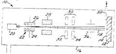
본 발명의 방법은 기판 위에 클러스터를 생성 및 증착시키기 위한 장치로 수행되는데, 이 장치의 한 형태가 제1도에 증착 장치(10)으로서 도시되어 있다. 표면(14)가 있는 기판(12)는 클러스터 비임 (18)이 표면(14)에 대해서 집중될 수 있도록 진공실(16)에 장착된다.The method of the present invention is carried out with an apparatus for creating and depositing clusters on a substrate, one form of which is shown as deposition apparatus 10 in FIG.
클러스터들은 초기에 초음파 노즐원(20)에서 발생된다. 현재의 클러스터 제조원(20)으로서 바람직한 유형을 제1도에서 개략적으로 설명하고, 제3도에서 더욱 상세하게 검토한다. 클러스터 중의 반응종의 성질에 따라 여러가지 유형의 노즐원이 사용될 수 있다.Clusters are initially generated at the
클러스터를 구성하는 물질은 "구조 단위(structural units)" 또는 "단위"로서 제공된다. 이 용어들은 본 명세서에 사용된 바와 같이, 반응종을 포함하는 원자, 단순 분자, 복합 분자, 또는 착물을 의미할 수 있다. 단위들은 증기원(20)에서 클러스터로 형성된다.The substances that make up the cluster are provided as "structural units" or "units". These terms, as used herein, may refer to atoms, simple molecules, complex molecules, or complexes containing reactive species. The units are formed in clusters in the
증기원(20)에 의해 방출된 클러스터들은 일반적으로 양호하게 평행화(平行化; collimation)되며, 전하를 운반하지 않는다. 클러스터들은 이온화기(22)로 들어가 전자 충격에 의해 다수의 클러스터들이 양(陽)으로 이온화 됨으로써, 클러스터들은 이어서 기판(12)를 향해 가속될 수 있다. 바람직한 이온화기(22)에서는 약 50-100 볼트의 양전위하에서 약 10-30 밀리암페어의 전류를 가지고 전자들이 음극(24)에서 양극(26)으로 방출된다. 전자들의 경로는 미리 이온화되지 않은 클러스터 비임(18)의 비행선을 가로질러 차단한다. 전자들 중 일부가 입자의 일부와 충돌하고, 그에 따라 입자들은 양으로 하전된다. 따라서, 클러스터 자체를 양으로 하전된 것으로 보고, 이하 이온들로 이루어지는 클러스터라기 보다는 단위들로 이루어지는 클러스터라고 말하는 것이 편리하다. 클러스터들이 기판(12)를 향해 조절 가능하게 가속될 수 있도록 낮은 이온화 수준이 요구된다.Clusters released by the
클러스터 비임(18) 중의 이온화된 클러스터들은 질량 분리기(28)로 들어가, 클러스터화되지 않은 원자 및 이온들과, 바람직한 크기보다 훨씬 크거나 작은 크기의 클러스터들이 제거된다. 표면(14)에 도달하는 대부분의 클러스터들은 최소 크기 이상이어야 한다. 즉, 각 클러스터 내의 최소 단위수를 초과하는 것이 바람직하다. 그렇지 않으면, 표면(14)에 충돌하여 클러스터가 붕해된 후, 반응종을 함유하고 있는 보다 작은 클러스터로부터 유래한 단위들은 과도한 에너지를 갖게 될 것이다. 이 과도한 에너지는 클러스터의 붕해 및 후속 화학 반응 도중 표면에 충돌 손상을 일으킬수 있다. 대부분의 표면 물질에 있어서 손상 역치는 단위당 20-50eV 범위이다.Ionized clusters in
질량 분위기(28)은 임의의 조작 가능한 방법에 의해 소정의 크기 범위보다 더 작은 이온 및 클러스터들을 제거한다. 질량 분리기는 정전기 또는 자기(磁氣)기술, 바람직하기로는 정전기 기술에 의해 소정의 크기보다 더 작은 크기의 이온 및 클러스터들을 분리할 수 있다. 필요에 따라서, 소정의 크기보다 더 큰 클러스터들은 제2분리 단계에서 잔존 범위로부터 분리시킴으로써, 오직 소정 크기의 범위를 갖는 클러스터만이 클러스터 비임 중에 잔존할 수 있다.
특정 크기 범위의 단일 이온화된 클러스터들을 주로 함유하는 클러스터 비임(18)은 이어서 정전 가속기(30)에 의해 기판(12)를 향해 가속되며, 가속기 중의 제 1유공(有孔, apertured) 전극(32)는 제2유공 전극(34)보다 더 양전위에서 유지된다. 이온화된 클러스터 비임(18)은 전극(32) 및 (34)의 소공을 통과하여 전위차에 의해 가속된다. 제2유공전극(34)는 전형적으로 제1유공전극(32)보다 약 1,000-10,000볼트 더 낮은 전압을 가지므로 이온화기(22)와 동일한 전압에서의 부유가 가능하게 된다. 1000개의 원자로 된 단일 하전된 클러스터가 1000볼트의 전압차가 유지된 전극(32) 및 (34)를 통과할 때 1000eV의 에너기가 비임의 클러스터에 가해진다. 클러스터의 이 고에너지 및 고질량은 클러스터가 기판(12)의 표면(14)를 침투할 수 있게 해 준다. 충동시 클러스터는 1-10eV의 비교적 작은 에너지를 갖는 클러스터의 각 단위들로 붕해된다. 단위당 작은 에너지는 단위가 표면(14)를 침투하는 것을 허용하지 않으며, 만일 침투하지 않을 경우 표면 및 표면상의 구조가 파괴될 것이다. 한편, 단위당 1-10eV 정도의 에너지는 피막의 균일한 표면 구조형성에 도움이 된다.The
에너지를 얻은 클러스터는 이어서 비임(18)를 좌우로 주사 또는 라스터(raster)시킬 수 있는 촛점 조정 및 편향 전극(36)으로 들어감으로써, 표면(14)위에 소정의 형태로 패턴을 형성할 수 있다. 일반적으로 표면(14)를 노출시켜야 할 경우, 전극(36)은 사용할 필요가 없다.The energized cluster can then form a pattern in the desired shape on the
장치(10)에서, 제1반응물은 클러스터 비임(18)로서 제공되고, 제2반응물은 제2의 외부원에 의해 제공되는 경우에 사용하기 위하여, 임의의 반응물 투입구(38)을 제공함으로써 표면(14)에 제2반응물을 도입시킬 수 있다. 이 실시 태양에서, 제2반응물은 클러스터화되지 않은 형태로 제공된다.In the apparatus 10, the first reactant is provided as a
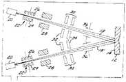
2개의 클러스터 비임 (18) 및 (18')를 동시에 표면(14)에 집중시킬 수 있도록 제2반응물은 클러스터 형태로도 역시 제공될 수 있다. 이 방법은 제2도에 도시되어 있는데, 여기에는 하나의 진공실(16)내에 2개의 장치(10)이 갖추어진다.The second reactant may also be provided in the form of a cluster so that two
제1도 또는 제2도의 장치 (10)에서, 클러스터들은 적당한 유형의 클러스터 공급원에 의해서 생성된다. 바람직한 펄스식 클러스터 공급원(40)이 제3도에 도시되어 있다. 펄스식 클러스터 공급원(40)은 클러스터로 형성하고자 하는 휘발성 물질을 공급하는 가스 라인(44)에 의해 압축되는 중공체(中空體) (42)를 포함한다. 밸브(80)은 가스 라인(44)로 가는 가스의 흐름을 조절한다. 임의의 제2가스 라인(45)는 제2가스를 중공체(42)에 공급할 수 있으며, 밸브(82)는 제2가스라인(45)로 가는 제2가스의 흐름을 조절한다. 펄스식 클러스터 공급원(40)은 오직 단일 가스, 또는 가스 혼합물을 가지고 작동시킬 수 있다. 제2가스가 사용될 경우에는, 이 가스는 중공체(42) 중에 동시에 또는 프로그램된 방식으로 도입되는 아르곤 등의 불활성 운반 가스일 수 있다. 또한, 제 2가스는 클러스터 비임 (18) 중의 클러스터들이 하나의 클러스터 내에 2종의 단위들을 모두 포함하는 그러한 제 2반응성 가스일 수도 있다.In the apparatus 10 of FIG. 1 or FIG. 2, clusters are created by a suitable type of cluster source. A preferred
가스는 통상 직경이 약 0.05㎝(약 0.02인치)인 좁은 목부(48)을 갖는 초음파 노즐(46)을 통해 분출된다. 가스가 이 목부(48)을 출발한 후 팽창하는 팽창부(50)의 최대 출구 직경은 목부(48)의 직경보다 더 크며, 통상 약 0.635㎝(약 1/4인치)이다. 분출된 가스는 초음파 노즐(46)을 통과하여 팽창되고, 반응종을 함유하는 단위군(單位群)들이 농축되어 클러스터를 형성한다. 가스가 팽창함에 따라 가스는 냉각되어 과포화되고, 이에 따라 가스 기류중에 작은 클러스터들의 균일한 핵생성이 유도된다. 또한, 핵생성은 불균일한 핵생성에 의해 펄스식 클러스터 공급원(40)의 초음파 노즐(46)의 내벽에서 일어날 수도 있다. 상기한 바와 같이, 클러스터 공급원(40)은 반응종을 함유하는 클러스터화 되지 않은 단위들, 소형 클러스터들, 소정의 크기를 갖는 클러스터들 및 대형 클러스터들을 생산한다. 소정의 크기를 갖는 클러스터들만이 질량 분리기(28)에 의해 선택된다.The gas is blown out through an
클러스터 공급원(40)은 목부(48)의 바로 상류 위치에 초음파 노즐(46)을 폐쇄하는 밸브 플런저 (52)를 제공함으로써 펄스 또는 불연속적인 방식으로 클러스터들을 분출하도록 만들 수 있다. 밸브 플런저 (52)는 통상 밸브 플런저 (52)의 축(56)에 대해서 작용하는 코일 스프링(54)에 의해 폐쇄된다. 이어서, 밸브 플런저(52)는 전자기 밸브 작동기(58)에 의해 개방 위치로 이동한다. 밸브 작동기(58)은 전류가 가해질 때 자기장을 형성하며, 자기장은 축(56)을 자기장 내로 이동시킨다.The
이 기계적인 구조를 사용하면, 밸브 플런저(52)는 폭발 또는 펄스 가스가 초음파 노즐(46)을 통해 방출될 수 있도록 신속하게 개방 및 폐쇄되도록 만들 수 있다. 사용율(duty cycle), 즉 가스가 클러스터 공급원 (40)을 통과하고 나서 다시 통과하는 데 걸리는 시간은 클러스터들의 수에 따라 클러스터 비임(18)로서 표면(14)에 전달되도록 선택 및 조절된다. 전형적인 사용율은 2밀리초 동안 통과시키고 (on), 98밀리초 동안 통과시키지 않음 (off)으로써 불연속적인 비임을 발생시킬 수 있다. 이와 같은 교대 사용율은 반응에 유리한 영향을 미치거나, 또는 펌핑 장치가 비교적 작거나 또는 매 가스폭발시마다 극히 높은 농도의 클러스터들이 요구되는 핌핑 장치에 대한 가스부하를 감소시키기 위해 사용될 수 있다. 용량이 큰 펌핑 장치를 사용할 수 있는 경우에는 교대 사용율이 필요하지 않을 수도 있다.Using this mechanical structure, the valve plunger 52 can be made to open and close quickly so that an explosion or pulsed gas can be released through the
본 발명의 바람직한 응용예로서 클러스터 비임(18)에 의해 표면(14)을 에칭하는 방법을 제4도에서 개략적으로 설명한다. 클러스터 비임(18)은 양호하게 평행화되어, 기판(12)에 선명하게 음각된 홈(60)을 에칭한다. 이런 유형의 응용에서 클러스터들은 기판(12)의 재료와 반응하여 표면(14)를 이탈할 수 있는 휘발성 반응생성물을 형성하는 반응물로 이루어지는 구조 단위들로 형성된다. 예를 들면, 기판(12)가 실리콘인 경우, CCl4, CF4, 또는 NF3와 같은 할로겐을 함유하는 반응종을 포함하는 단위들로부터 클러스터들을 형성함으로써 홈(60)을 표면(14)에 에칭시킬 수 있다. 에너지를 얻은 클러스터들은 표면과 충돌시 붕해되고, 할로겐은 실리콘과 반응하여 휘발성 반응 생성물을 형성한다. 이 반응은 평행화된 클러스터 비임(18)이 표면(14)와 만나는 영역으로 제한되며, 클러스터 비임이 표면상에서 충돌하는 패턴으로 기판 재료를 효과적으로 제거한다.As a preferred application of the present invention, a method of etching the
본 발명의 또다른 바람직한 실시 상태가 제5도에 도시되어 있다. 제5도에서 클러스터 비임(18)의 단위로서 공급된 반응물은 기판(12)를 구성하는 재료와 반응하여 기판(12)의 표면위에 반응 생성물 피막(62)를 형성한다. 피막(62)는 기판 반응물 및 클러스터 비임으로부터의 반응물이 피막(62)를 통해 서로 맞닿아 더 이상 확산되지 않을때까지 그 두께가 성장하여 피막(62)에 더 많은 반응생성물을 형성한다. 따라서, 피막(62)의 성장은 그 자체를 제한한고 있다. 피막(62)의 이런 유형의 성장례는 기판(12)가 실리콘이고, 클러스터 비임(18)이 질소 또는 산소를 갖는 단위들을 함유함으로써 에너지를 얻는 반응에서 질화규소나 산화규소 피막(62)가 형성되는 경우에 일어난다.Another preferred embodiment of the invention is shown in FIG. In FIG. 5, the reactant supplied as a unit of the
제5도는 또한 또 다른 바람직한 실시 상태를 설명하기 위해 사용될 수 있다. 다른 방법에서, 피막(62)는 클러스터 비임(18)로서 공급되어 표면(14)위에 피막으로서 잔존하는 반응 생성물을 형성하는 단위들의 분해에 의해 형성된다. 이런 유형의 피막은 바응종이 클러스터 비임으로 공급되는 한, 무한정 두꺼워질 수 있다. 이런 유형의 반응예로서는 표면에 대해서 W(CO)6의 클러스터를 집중시킴으로써 표면에 텅스텐 피막을 형성하는 반응을 들 수 있다. 클러스트들이 붕해됨으로써 에너지를 얻는 반응에서 W(CO)6분자들은 분해되어 표면에 텅스텐 반응 생성물을 증착시킨다. 일산화탄소, 즉 휘발성 반응 생성물은 표면을 이탈하여 진공 장치를 통해 펌핑된다.5 may also be used to illustrate another preferred embodiment. In another method, the
본 발명의 또 다른 바람직한 실시예가 제6도에 도시되어 있다. 이 실시예에서 제1반응물은 클러스터 비임(18)의 단위로서 공급되고, 제2반응물은 다른 외부원, 즉 본 실시예에서 제 1반응물은 클러스터 비임(18)의 단위로서 공급되고, 제 2반응물은 다른 외부원, 즉 본 실시예에서는 투입구(38)로부터 표면(14)의 상부영역에 공급된다. 공급된 제2반응물은 표면(14)의 상부에 반응물운(反應物雲, reactant cloud)(64)를 형성한다. 방응물운 중의 반응물은 표면(14)에 에너지를 얻은 반응종과 반응하며 표면 클러스터 비임(18)의 작용을 통해 증착되고 에너지를 얻게 된다. 고체 반응 생성물은 잔류하여 피막(66)을 형성하는 반면에, 휘발성 반응 생성물은 표면으로부터 이탈되어 펌핑된다. 이런 유형의 반응례에서는 클러스터 비임의 클러스터로서 에너지를 갖고 있는 AsH3반응물을 공급하고, 투입구(38)를 통해 테트라메틸갈륨을 공급하는 반응을 들 수 있다. 이 두가지 반응물은 반응하여 피막(66) 형태로 비소화갈륨 반응 생성물을 생성하고, 수소 및 메탄의 휘발성 반응 생성물은 표면을 이탈한다.Another preferred embodiment of the present invention is shown in FIG. In this embodiment the first reactant is supplied as a unit of the
또 다른 바람직한 실시예가 제 7도에 설명되어 있다. 이 실시예에서는 제 2도에 나타낸 장치를 사용하여 에너지를 갖게 된 2종의 반응물을 표면(14)에 대해서 집중시켰다. 두가지 반응물은 2개의 별도의 클러스터 공급원 및 비임 조절 장치에 의해 생성된 2개의 분리된 클러스터 비임(18) 및 (18')로서 공급된다. 또한, 고체 반응 생성물은 표면(14)에 잔류하여 피막(68)를 형성하고, 휘발성 반응 생성물은 표면에서 이탈되어 펌핑된다. 이와 같은 2중으로 에너지를 얻는 반응례로서는 2가지 반응성 실란 및 메탄(또는 프로판)가스의 클러스터를 동시에 분사함으로써 탄화규소를 형성하는 것을 들 수 있다. 이제, 본 발명의 방법은 클러스터 비임 중의 클러스터로서 적어도 1종의 반응물을 공급함으로써 에너지를 얻는 표면 화학 반응을 유도하는 신규 방법을 제공한다는 것을 이해할 것이다. 클러스터들이 표면에서 붕해될 때, 비임중의 반응물 및 비임의 에너지가 표면에 방출된다. 반응물에 전달되는 에너지는 충분하며, 외부 에너지원을 반응물에 연결할 필요가 없다. 기판은 그의 저면으로부터 적당히 냉각될 수 있다. 에너지를 얻은 반응물은 이어서 표면 화학 반응 상태로 들어간다.Another preferred embodiment is described in FIG. In this example, the two reactants, which are energized, are concentrated on the
예시의 목적상 본 발명의 특정 실시예를 가지고 상세히 설명하였지만, 본 발명의 정신 및 범위로부터 벗어남이 없이 여러가지 변형을 가할 수 있다. 따라서, 본 발명은 단지 첨부된 특허청구의 범위에 의해서만 한정되어서는 아니 된다 .While specific embodiments of the invention have been described in detail for purposes of illustration, various modifications may be made without departing from the spirit and scope of the invention. Therefore, the present invention should not be limited only by the appended claims.
Claims (17)
Translated fromKoreanApplications Claiming Priority (4)
| Application Number | Priority Date | Filing Date | Title |
|---|---|---|---|
| US0L7380 | 1987-02-20 | ||
| US017,380 | 1987-02-20 | ||
| US07/017,380US4740267A (en) | 1987-02-20 | 1987-02-20 | Energy intensive surface reactions using a cluster beam |
| PCT/US1987/003043WO1988006194A1 (en) | 1987-02-20 | 1987-11-19 | Energy intensive surface reactions using a cluster beam |
Publications (2)
| Publication Number | Publication Date |
|---|---|
| KR890700693A KR890700693A (en) | 1989-04-26 |
| KR910001773B1true KR910001773B1 (en) | 1991-03-23 |
Family
ID=21782265
Family Applications (1)
| Application Number | Title | Priority Date | Filing Date |
|---|---|---|---|
| KR1019880701310AExpiredKR910001773B1 (en) | 1987-02-20 | 1987-11-19 | Energy focused surface reaction using cluster beams |
Country Status (7)
| Country | Link |
|---|---|
| US (1) | US4740267A (en) |
| EP (1) | EP0417067B1 (en) |
| JP (1) | JPH01502203A (en) |
| KR (1) | KR910001773B1 (en) |
| DE (1) | DE3789814T2 (en) |
| HK (1) | HK107394A (en) |
| WO (1) | WO1988006194A1 (en) |
Families Citing this family (50)
| Publication number | Priority date | Publication date | Assignee | Title |
|---|---|---|---|---|
| DE3628443C1 (en)* | 1986-08-21 | 1988-02-11 | Dornier System Gmbh | Process for the production of amorphous layers |
| US5031408A (en)* | 1988-04-19 | 1991-07-16 | The Boeing Company | Film deposition system |
| US4902572A (en)* | 1988-04-19 | 1990-02-20 | The Boeing Company | Film deposition system |
| US5030319A (en)* | 1988-12-27 | 1991-07-09 | Kabushiki Kaisha Toshiba | Method of oxide etching with condensed plasma reaction product |
| JPH03111578A (en)* | 1989-06-29 | 1991-05-13 | Toshiba Corp | Thin film forming method and thin film forming apparatus |
| US5082685A (en)* | 1989-07-24 | 1992-01-21 | Tdk Corporation | Method of conducting plasma treatment |
| US5205902A (en)* | 1989-08-18 | 1993-04-27 | Galileo Electro-Optics Corporation | Method of manufacturing microchannel electron multipliers |
| US5015323A (en)* | 1989-10-10 | 1991-05-14 | The United States Of America As Represented By The Secretary Of Commerce | Multi-tipped field-emission tool for nanostructure fabrication |
| JPH0452273A (en)* | 1990-06-18 | 1992-02-20 | Mitsubishi Electric Corp | Thin film forming equipment |
| JP2662321B2 (en)* | 1991-05-31 | 1997-10-08 | 科学技術振興事業団 | Surface treatment method using ultra-slow cluster ion beam |
| US5286331A (en)* | 1991-11-01 | 1994-02-15 | International Business Machines Corporation | Supersonic molecular beam etching of surfaces |
| DE4227237C2 (en)* | 1992-08-19 | 1995-08-10 | Juergen Dr Gspann | Process for agglomerate beam lithography |
| JPH0737807A (en)* | 1993-07-21 | 1995-02-07 | Hitachi Ltd | Surface treatment method using atomic and molecular beams and apparatus therefor |
| EP0652308B1 (en)* | 1993-10-14 | 2002-03-27 | Neuralsystems Corporation | Method of and apparatus for forming single-crystalline thin film |
| KR100192228B1 (en)* | 1995-08-04 | 1999-06-15 | 한갑수 | Manufacturing Method of Tin Oxide Thin Film |
| US6162512A (en)* | 1996-04-19 | 2000-12-19 | Korea Institute Of Science And Technology | Process for modifying surfaces of nitride, and nitride having surfaces modified thereby |
| US6152074A (en)* | 1996-10-30 | 2000-11-28 | Applied Materials, Inc. | Deposition of a thin film on a substrate using a multi-beam source |
| DE19713637C2 (en) | 1997-04-02 | 1999-02-18 | Max Planck Gesellschaft | Particle manipulation |
| JP3036506B2 (en)* | 1998-02-26 | 2000-04-24 | 日本電気株式会社 | Method of manufacturing batch aperture for electron beam exposure apparatus |
| DE19814871A1 (en)* | 1998-04-02 | 1999-10-07 | Max Planck Gesellschaft | Method and device for targeted particle manipulation and deposition |
| WO2000036631A1 (en)* | 1998-12-11 | 2000-06-22 | Surface Technology Systems Limited | Plasma processing apparatus |
| US6375790B1 (en) | 1999-07-19 | 2002-04-23 | Epion Corporation | Adaptive GCIB for smoothing surfaces |
| US6613240B2 (en)* | 1999-12-06 | 2003-09-02 | Epion Corporation | Method and apparatus for smoothing thin conductive films by gas cluster ion beam |
| US6498107B1 (en) | 2000-05-01 | 2002-12-24 | Epion Corporation | Interface control for film deposition by gas-cluster ion-beam processing |
| AUPR179500A0 (en)* | 2000-11-30 | 2000-12-21 | Saintech Pty Limited | Ion source |
| US20030019428A1 (en)* | 2001-04-28 | 2003-01-30 | Applied Materials, Inc. | Chemical vapor deposition chamber |
| JP2005512312A (en)* | 2001-10-11 | 2005-04-28 | エピオン コーポレイション | GCIB processing to improve interconnect vias and improved interconnect vias |
| WO2004044954A2 (en)* | 2002-11-08 | 2004-05-27 | Epion Corporation | Gcib processing of integrated circuit interconnect structures |
| US7154086B2 (en)* | 2003-03-19 | 2006-12-26 | Burle Technologies, Inc. | Conductive tube for use as a reflectron lens |
| US20080073516A1 (en)* | 2006-03-10 | 2008-03-27 | Laprade Bruce N | Resistive glass structures used to shape electric fields in analytical instruments |
| EP2747120B1 (en)* | 2006-10-30 | 2017-12-20 | Japan Aviation Electronics Industry, Limited | Method of smoothing solid surface with gas cluster ion beam |
| US8835880B2 (en)* | 2006-10-31 | 2014-09-16 | Fei Company | Charged particle-beam processing using a cluster source |
| US8303833B2 (en)* | 2007-06-21 | 2012-11-06 | Fei Company | High resolution plasma etch |
| US8372489B2 (en)* | 2007-09-28 | 2013-02-12 | Tel Epion Inc. | Method for directional deposition using a gas cluster ion beam |
| US7794798B2 (en)* | 2007-09-29 | 2010-09-14 | Tel Epion Inc. | Method for depositing films using gas cluster ion beam processing |
| US20090233004A1 (en)* | 2008-03-17 | 2009-09-17 | Tel Epion Inc. | Method and system for depositing silicon carbide film using a gas cluster ion beam |
| US20090314963A1 (en)* | 2008-06-24 | 2009-12-24 | Tel Epion Inc. | Method for forming trench isolation |
| US8202435B2 (en)* | 2008-08-01 | 2012-06-19 | Tel Epion Inc. | Method for selectively etching areas of a substrate using a gas cluster ion beam |
| US8313663B2 (en) | 2008-09-24 | 2012-11-20 | Tel Epion Inc. | Surface profile adjustment using gas cluster ion beam processing |
| US8304033B2 (en)* | 2009-02-04 | 2012-11-06 | Tel Epion Inc. | Method of irradiating substrate with gas cluster ion beam formed from multiple gas nozzles |
| US8097860B2 (en)* | 2009-02-04 | 2012-01-17 | Tel Epion Inc. | Multiple nozzle gas cluster ion beam processing system and method of operating |
| US20100193898A1 (en)* | 2009-02-04 | 2010-08-05 | Tel Epion Inc. | Method for forming trench isolation using gas cluster ion beam processing |
| US7968422B2 (en)* | 2009-02-09 | 2011-06-28 | Tel Epion Inc. | Method for forming trench isolation using a gas cluster ion beam growth process |
| US8237136B2 (en)* | 2009-10-08 | 2012-08-07 | Tel Epion Inc. | Method and system for tilting a substrate during gas cluster ion beam processing |
| US20110084214A1 (en)* | 2009-10-08 | 2011-04-14 | Tel Epion Inc. | Gas cluster ion beam processing method for preparing an isolation layer in non-planar gate structures |
| US8048788B2 (en)* | 2009-10-08 | 2011-11-01 | Tel Epion Inc. | Method for treating non-planar structures using gas cluster ion beam processing |
| US8338806B2 (en) | 2010-05-05 | 2012-12-25 | Tel Epion Inc. | Gas cluster ion beam system with rapid gas switching apparatus |
| US8173980B2 (en) | 2010-05-05 | 2012-05-08 | Tel Epion Inc. | Gas cluster ion beam system with cleaning apparatus |
| US9540725B2 (en) | 2014-05-14 | 2017-01-10 | Tel Epion Inc. | Method and apparatus for beam deflection in a gas cluster ion beam system |
| DE102016119791A1 (en)* | 2016-10-18 | 2018-04-19 | scia Systems GmbH | Method and device for processing a surface of a substrate by means of a particle beam |
Family Cites Families (7)
| Publication number | Priority date | Publication date | Assignee | Title |
|---|---|---|---|---|
| US4218495A (en)* | 1975-07-18 | 1980-08-19 | Futaba Denshi Kogyo K.K. | Schottky barrier type solid-state element |
| EP0061906B1 (en)* | 1981-03-26 | 1987-06-10 | Inoue-Japax Research Incorporated | A method of, and an apparatus for, processing a workpiece with energetic particles and a product processed thereby |
| JPS58106750A (en)* | 1981-12-18 | 1983-06-25 | Toshiba Corp | Focused ion beam processing method |
| US4541890A (en)* | 1982-06-01 | 1985-09-17 | International Business Machines Corporation | Hall ion generator for working surfaces with a low energy high intensity ion beam |
| US4411733A (en)* | 1982-06-18 | 1983-10-25 | Bell Telephone Laboratories, Incorporated | SPER Device for material working |
| JPS59207631A (en)* | 1983-05-11 | 1984-11-24 | Semiconductor Res Found | Dry process employing photochemistry |
| US4559096A (en)* | 1984-06-25 | 1985-12-17 | The United States Of America As Represented By The United States Department Of Energy | Method of precisely modifying predetermined surface layers of a workpiece by cluster ion impact therewith |
- 1987
- 1987-02-20USUS07/017,380patent/US4740267A/ennot_activeExpired - Lifetime
- 1987-11-19DEDE3789814Tpatent/DE3789814T2/ennot_activeExpired - Fee Related
- 1987-11-19WOPCT/US1987/003043patent/WO1988006194A1/enactiveIP Right Grant
- 1987-11-19KRKR1019880701310Apatent/KR910001773B1/ennot_activeExpired
- 1987-11-19EPEP88900287Apatent/EP0417067B1/ennot_activeExpired - Lifetime
- 1987-11-19JPJP88500653Apatent/JPH01502203A/enactiveGranted
- 1994
- 1994-10-06HKHK107394Apatent/HK107394A/enunknown
Also Published As
| Publication number | Publication date |
|---|---|
| JPH01502203A (en) | 1989-08-03 |
| EP0417067A1 (en) | 1991-03-20 |
| HK107394A (en) | 1994-10-14 |
| DE3789814D1 (en) | 1994-06-16 |
| WO1988006194A1 (en) | 1988-08-25 |
| EP0417067B1 (en) | 1994-05-11 |
| JPH0548301B2 (en) | 1993-07-21 |
| US4740267A (en) | 1988-04-26 |
| DE3789814T2 (en) | 1994-08-25 |
| KR890700693A (en) | 1989-04-26 |
Similar Documents
| Publication | Publication Date | Title |
|---|---|---|
| KR910001773B1 (en) | Energy focused surface reaction using cluster beams | |
| US6207282B1 (en) | Substrate surface treatment method | |
| JP4926067B2 (en) | Ionizer and method for gas cluster ion beam formation | |
| US7060989B2 (en) | Method and apparatus for improved processing with a gas-cluster ion beam | |
| US8328982B1 (en) | Low-temperature, converging, reactive gas source and method of use | |
| KR100242483B1 (en) | Neutral Particle Beam Irradiation Apparatus | |
| US7855374B2 (en) | Gas cluster ion beam emitting apparatus and method for ionization of gas cluster | |
| JPH06275545A (en) | Formation of compound thin film using gas cluster ion | |
| US5640009A (en) | Fast atom beam source | |
| EP0183254A2 (en) | Plasma CVD apparatus and method for forming a diamond-like carbon film | |
| US5089289A (en) | Method of forming thin films | |
| CN113181855A (en) | Method for completing reaction and etching on surface by using cluster beam energy | |
| JP3363040B2 (en) | Fast atom beam source | |
| JP3582885B2 (en) | Method and apparatus for smoothing diamond | |
| CN112151349A (en) | Apparatus and method for reducing particle contamination in gas cluster ion beam processing equipment | |
| JPH08259400A (en) | Diamond etching method and apparatus | |
| JPH09223594A (en) | Beam source and micro-working method | |
| US5231259A (en) | Radiation manufacturing apparatus | |
| KR900008155B1 (en) | Thin film formation method and apparatus | |
| JP2000265277A (en) | Formation of film using electron beam plasma | |
| RU2620534C2 (en) | Method of coating and device for its implementation | |
| JPH07335395A (en) | Plasma generation method and film forming method, etching method, semiconductor deposition method and doping method using the same | |
| JPH03219597A (en) | High speed atomic beam radiator | |
| JPS63216964A (en) | Thin film forming equipment | |
| JP2004530792A (en) | Method of forming nanocrystal beam |
Legal Events
| Date | Code | Title | Description |
|---|---|---|---|
| A201 | Request for examination | ||
| PA0105 | International application | St.27 status event code:A-0-1-A10-A15-nap-PA0105 | |
| PA0201 | Request for examination | St.27 status event code:A-1-2-D10-D11-exm-PA0201 | |
| R17-X000 | Change to representative recorded | St.27 status event code:A-3-3-R10-R17-oth-X000 | |
| PG1501 | Laying open of application | St.27 status event code:A-1-1-Q10-Q12-nap-PG1501 | |
| E902 | Notification of reason for refusal | ||
| PE0902 | Notice of grounds for rejection | St.27 status event code:A-1-2-D10-D21-exm-PE0902 | |
| P11-X000 | Amendment of application requested | St.27 status event code:A-2-2-P10-P11-nap-X000 | |
| P13-X000 | Application amended | St.27 status event code:A-2-2-P10-P13-nap-X000 | |
| G160 | Decision to publish patent application | ||
| PG1605 | Publication of application before grant of patent | St.27 status event code:A-2-2-Q10-Q13-nap-PG1605 | |
| E701 | Decision to grant or registration of patent right | ||
| PE0701 | Decision of registration | St.27 status event code:A-1-2-D10-D22-exm-PE0701 | |
| GRNT | Written decision to grant | ||
| PR0701 | Registration of establishment | St.27 status event code:A-2-4-F10-F11-exm-PR0701 | |
| PR1002 | Payment of registration fee | St.27 status event code:A-2-2-U10-U12-oth-PR1002 Fee payment year number:1 | |
| FPAY | Annual fee payment | Payment date:19940304 Year of fee payment:4 | |
| PR1001 | Payment of annual fee | St.27 status event code:A-4-4-U10-U11-oth-PR1001 Fee payment year number:4 | |
| LAPS | Lapse due to unpaid annual fee | ||
| PC1903 | Unpaid annual fee | St.27 status event code:A-4-4-U10-U13-oth-PC1903 Not in force date:19950324 Payment event data comment text:Termination Category : DEFAULT_OF_REGISTRATION_FEE | |
| PC1903 | Unpaid annual fee | St.27 status event code:N-4-6-H10-H13-oth-PC1903 Ip right cessation event data comment text:Termination Category : DEFAULT_OF_REGISTRATION_FEE Not in force date:19950324 |