KR910000178B1 - Framing timing extraction circuit - Google Patents
Framing timing extraction circuitDownload PDFInfo
- Publication number
- KR910000178B1 KR910000178B1KR1019900011866AKR900011866AKR910000178B1KR 910000178 B1KR910000178 B1KR 910000178B1KR 1019900011866 AKR1019900011866 AKR 1019900011866AKR 900011866 AKR900011866 AKR 900011866AKR 910000178 B1KR910000178 B1KR 910000178B1
- Authority
- KR
- South Korea
- Prior art keywords
- signal
- error
- bits
- data
- bit
- Prior art date
- Legal status (The legal status is an assumption and is not a legal conclusion. Google has not performed a legal analysis and makes no representation as to the accuracy of the status listed.)
- Expired
Links
Images


Classifications
- H—ELECTRICITY
- H04—ELECTRIC COMMUNICATION TECHNIQUE
- H04N—PICTORIAL COMMUNICATION, e.g. TELEVISION
- H04N7/00—Television systems
- H04N7/08—Systems for the simultaneous or sequential transmission of more than one television signal, e.g. additional information signals, the signals occupying wholly or partially the same frequency band, e.g. by time division
- H—ELECTRICITY
- H03—ELECTRONIC CIRCUITRY
- H03M—CODING; DECODING; CODE CONVERSION IN GENERAL
- H03M13/00—Coding, decoding or code conversion, for error detection or error correction; Coding theory basic assumptions; Coding bounds; Error probability evaluation methods; Channel models; Simulation or testing of codes
- H03M13/37—Decoding methods or techniques, not specific to the particular type of coding provided for in groups H03M13/03 - H03M13/35
- H03M13/43—Majority logic or threshold decoding
Landscapes
- Engineering & Computer Science (AREA)
- Physics & Mathematics (AREA)
- Probability & Statistics with Applications (AREA)
- Theoretical Computer Science (AREA)
- Multimedia (AREA)
- Signal Processing (AREA)
- Error Detection And Correction (AREA)
- Detection And Prevention Of Errors In Transmission (AREA)
Abstract
Translated fromKoreanDescription
Translated fromKorean제1도는 야외 실험에서 수신된 데이타의 에러 비트수 분포의 평균치의 예를 나타낸 도면.1 is a diagram showing an example of an average value of error bit number distributions of data received in an outdoor experiment.
제2도는 야외 실험에서 송수신된 신호를 삽입 배열한 경우 수신 데이타의 에러 비트수 분포의 평균치의 예를 나타낸 도면.2 is a diagram showing an example of an average value of the distribution of the number of error bits of received data when the signals transmitted and received are inserted and arranged in an outdoor experiment.
제3도는 1 패킷(packet)중의 에러 비트수의 분포를 나타낸 도면.3 is a diagram showing the distribution of the number of error bits in one packet.
제4도는 파형 왜곡 지역에서 1 패킷중의 에러 비트수의 분포를 나타낸 도면.4 is a diagram showing the distribution of the number of error bits in one packet in a waveform distortion area.
제5도 및 제6도는 임펄스 지역 및 파형 왜곡 지역에 있는 각각의 1 패킷중의 에러 버스트 길이의 분포를 나타낸 도면.5 and 6 show the distribution of error burst lengths in each packet in the impulse region and the waveform distortion region.
제7도 및 제8도는 전형적인 임펄스 지역 및 파형 왜곡 지역에 있는 각각의 b/n(%)에 대한 에러 블럭의 주파수비의 누적 분포를 나타낸 도면.7 and 8 show the cumulative distribution of the frequency ratios of the error blocks for each b / n (%) in the typical impulse region and the waveform distortion region.
제9도는 에러 정정 및 디코딩 회로의 구성의 일례를 나타낸 블럭선도.9 is a block diagram showing an example of the configuration of an error correction and decoding circuit.
제10도는 본 발명에 따른 신호 송신 회로의 일례를 나타낸 블럭선도.10 is a block diagram showing an example of a signal transmission circuit according to the present invention.
제11도는 본 발명에 따른 에러 정정 및 디코딩 회로의 다른 일례에 대한 블럭선도.11 is a block diagram of another example of an error correction and decoding circuit according to the present invention.
제12도는 본 발명에 따른 실제 문자 코드 방송용 수신기에 적용되는 회로의 블럭선도.12 is a block diagram of a circuit applied to an actual character code broadcasting receiver according to the present invention.
제13도는 본 발명에 따른 다수결 논리 회로의 블럭선도.13 is a block diagram of a majority vote logic circuit in accordance with the present invention.
제14도는 본 발명에 따른 에러 정정 동작에 관한 플로우챠트.14 is a flowchart of an error correction operation according to the present invention.
제15도는 본 발명을 실시하는데 이용되는 회로예에 대한 블럭선도.Fig. 15 is a block diagram of a circuit example used to implement the present invention.
제16도는 문자 코드 방송 시스템에 사용되는 패킷 신호예에 대한 파형도.16 is a waveform diagram for an example of a packet signal used in a character code broadcasting system.
제17도는 본 발명에 따른 패킷 신호에 대한 제1예를 나타낸 도면.17 shows a first example of a packet signal according to the present invention.
제18도는 본 발명에 따른 패킷 신호에 대한 제2예를 나타낸 도면.18 shows a second example of a packet signal according to the present invention;
제19도는 본 발명에 따른 패킷 신호에 대한 제3예를 나타낸 도면.19 shows a third example of a packet signal according to the present invention;
제20도는 제19도에 도시된 바와 같이 각각의 비트 정보의 반전 정보를 가한 패킷 신호의 제4예에 있어서의 혼신호 디코딩용 ROM의 일례로 나타낸 도면.FIG. 20 is a diagram showing an example of a mixed-signal decoding ROM in the fourth example of a packet signal to which inversion information of each bit information is added as shown in FIG.
제21도는 본 발명에 따른 제1에러 정정 및 검출 회로에 대한 블럭선도.21 is a block diagram of a first error correction and detection circuit in accordance with the present invention.
제22도는 제1에러 정정 및 검출 회로의 제어 순서에 대한 플로우챠트.22 is a flowchart of the control sequence of the first error correction and detection circuit.
제23도는 본 발명에 따른 제2에러 정정 및 검출 회로에 대한 블럭선도.23 is a block diagram of a second error correction and detection circuit in accordance with the present invention.
제24도는 제2에러 정정 및 검출 회로의 제어 순서에 대한 플로우챠트.24 is a flowchart of the control sequence of the second error correction and detection circuit.
제25도는 다수결 논리 회로의 작동 설명도.25 is an operation explanatory diagram of a majority vote logic circuit.
제26도는 본 발명에 따른 에러 검출 회로예에 대한 블록선도.26 is a block diagram of an error detection circuit example according to the present invention.
제27도는 컴퓨터 시뮬레이션에 의해 에러가 정정된 후 정확한 수신율을 나타낸 도면.FIG. 27 is a diagram showing an accurate reception rate after an error is corrected by computer simulation.
제28a도, 제28b도, 제28c도 및 제28d도는 제1도의 에러 정정 및 검출회로의 동작 순서에 대한 플로우챠트.28A, 28B, 28C, and 28D are flowcharts for the operation sequence of the error correction and detection circuit of FIG.
제29도는 에러 검출 회로의 다른 예에 대한 블럭선도.29 is a block diagram of another example of an error detection circuit.
제30도는 전송된 분자 코드 신호 구성에 대한 선두.30 is the head of the transmitted molecular code signal configuration.
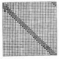
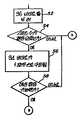
제31도는 본 발명에 따른 페레이밍(framing) 타이밍 추출 원리는 설명하기 위한 예시도.31 is an exemplary diagram for explaining the principle of framing timing extraction according to the present invention.
제32도는 본 발명을 적용한 일실시예에 의한 전송될 신호의 구성도.32 is a block diagram of a signal to be transmitted according to an embodiment of the present invention.
제33도는 중앙 처리 장치(CPU)에 가해진 후의 패킷 신호를 나타낸 도면.FIG. 33 shows packet signals after being applied to a central processing unit (CPU). FIG.
제34도는 수신측에서의 비트 조작(에러 프레이밍 타이밍)을 설명하기 위한 도면.34 is a diagram for explaining bit manipulation (error framing timing) on the receiving side.
제35도는 수신측에서의 비트 조작(정확한 프레이밍 타이밍)을 설명하기 위한 도면.35 is a diagram for explaining bit manipulation (accurate framing timing) on the receiving side.
제36a도 및 제36b도는 본 발명에 따른 패킷 신호 에러 정정 순서에 대한 플로우챠트.36A and 36B are flowcharts for a packet signal error correction procedure according to the present invention.
제37도는 본 발명에 따른 신호 취입(fetching)회로에 대한 블럭선도.37 is a block diagram of a signal fetching circuit according to the present invention.
제38도는 클럭-런-인(clock-rum-in) 신호의 유무를 검출하는 회로예에 대한 블럭선도.38 is a block diagram of a circuit example for detecting the presence or absence of a clock-rum-in signal.
제39도는 CPU의 RAM에 기억된 36 바이트 데이타를 표시한 도면.FIG. 39 shows 36-byte data stored in the RAM of the CPU. FIG.
제40도는 본 발명에 사용될 실제 프레이밍 위상 검색 순서에 대한 플로우챠트.40 is a flowchart for the actual framing phase search order to be used in the present invention.
* 도면의 주요부분에 대한 부호의 설명* Explanation of symbols for main parts of the drawings
101,302,403,609,1106,2109 : 신드롬 레지스터101,302,403,609,1106,2109: syndrome register
109,341,405,612,1107,1302,1501,2110 : 다수결 논리 회로109,341,405,612,1107,1302,1501,2110: Majority logic circuit
201 : 패리티 레지스터 301,404,632,1103,2103 : 데이타 레지스터201:
412,1109 : 에러 상태 레지스터 408 : 펄스 발생기412,1109: error status register 408: pulse generator
409 : 로드 및 정정 레지스터 509,2402 : 비교기409: Load and
611 : 에러 상태 레지스터 601,1104,1301,2108,3806 : 타이밍 발생기611:
1108 : 정정 게이트 회로 1105 : 로드 게이트 회로1108: correction gate circuit 1105: load gate circuit
1300 : 데이타 선택기 1502 : 감산 회로1300: data selector 1502: subtraction circuit
2118 : 에러 검출 회로 2400 : 인코더2118: error detection circuit 2400: encoder
2401 : 카운터 2402 : 카운터2401: counter 2402: counter
3801 : 지연 회로 3802 : 어드레스 제어 장치3801: delay circuit 3802: address control device
3005 : 에러 정정 회로3005: error correction circuit
본 발명은 TV 신호의 수직 귀선 소거 기간 동안에 디지털 신호로서 코드화된 문자, 도형 정보를 다중 전송하는 코드 방식 문자 방송에 적합한 코드의 에러 제어에 관한 것으로서, 특히, 문자 코드 방송 시스템에 사용하기 위한 프레이밍 타이밍 검출 회로에 관한 것이다.BACKGROUND OF THE
텔레비젼 신호를 사용함으로써 문자 및 그래프를 일반 가정용 텔레비젼 수상기의 표시기에 표시하기 위해 실제 문자 방송 시스템(유럽 및 북미에서는 문자 방송임)은 여러 나라에게 급속히 실현되어 가고 있다. 이 시스템에서 문자 및 그래픽 정보는 디지털 코드로 변환되고 수직 귀선 소거 기간동안 텔레비젼 신호와 다중 송신된다.By using television signals, real text broadcasting systems (which are text broadcasts in Europe and North America) are rapidly being realized in many countries to display text and graphs on the indicators of ordinary home television receivers. In this system, character and graphic information is converted into digital codes and multiplexed with the television signal during the vertical blanking period.
문자 방송으로는 두가지 방식을 생각할 수 있다. 즉, 문자 및 그래픽 정보를 도트(dot) 형태로 분리시킴으로써 문자 및 그래픽 정보를 전송하는 패턴 방식 문자 방송과, 문자 및 그래픽 정보를 코드로 변환함으로써 문자 및 그래픽 정보를 전송하는 패턴 방식 문자 방송과, 문자 및 그래픽 정보를 코드로 변환함으로써 문자 및 그래픽 정보를 전송하는 코드 방식 문자 방송이 있다. 패턴 방식 문자 방송은 일본의 무선 기술 상담에 의한 보고서가 체신청 장관에서 제출된 후 1982년 12월 일본에서 문자 방송용 표준 방식으로 공식적으로 설정되었다. 한편 코드 방식 문자 방송은 이제까지 개발된 패턴 방식 문자 방송과 겸용될 수 있고 코드화 신호를 이용할 경우 여러 종류의 서비스를 통신할 수도 있는 것으로 생각된다.There are two ways to think about text broadcasting. That is, a pattern type text broadcast for transmitting character and graphic information by separating text and graphic information into dots, and a pattern type text broadcast for transmitting text and graphic information by converting text and graphic information into codes; There is a coded text broadcast that transmits text and graphic information by converting text and graphic information into codes. Pattern-type text broadcasting was officially established in December 1982 as the standard method for text broadcasting in Japan after a report by the Japanese Radio Technology Consultation was submitted by the Minister of Communications. On the other hand, it is thought that coded text broadcasting can be combined with the patterned text broadcasting developed so far and that various types of services can be communicated using coded signals.
코드 방식 문자 방송은 패턴 방식 문자 방송에 비해 고전송 효율, 시스템의 다양성 및 고신장력 등과 같은 장점을 구비한다. 그러나 다른 한편으로는 코드 바식 문자 방송은 수상기의 문자 발생기용으로 사용될 고가의 ROM과, 전송 선로에 비트 에러가 있을 경우 에러 정보가 표시되는 것과 같은 단점을 구비한다. 그러나 최근의 LSI 기술의 진보와 워드 프로세서의 광범위한 보급 및 이용에 따라 ROM의 가격은 대량 생산으로 낮아지고 있다.Code-based text broadcasting has advantages such as high transmission efficiency, system versatility, and high tension compared to pattern-based text broadcasting. On the other hand, code bar text broadcasting has disadvantages such as expensive ROM to be used for the character generator of the receiver and error information displayed when there is a bit error in the transmission line. However, with the recent advances in LSI technology and the widespread adoption and utilization of word processors, the price of ROM has been reduced to mass production.
이미 언급된 일본의 실험적 문자 코드 방송 시스템에서는 8 비트나 16 비트를 포함하는 블록 중의 1 비트의 에러를 정정하기 위해 (8,4) 해밍(Hamming) 코드와 (8,4), 해밍 코드(16,11)가 사용되었다. 이 시스템은 비트 에러가 작은 우수한 전송 선로와 함께 사용되도록 하나 많은 임펄스 잡음이 실재하여 한 연속 비트 주기동안 한 블록에 비트 에러가 실재하게 될 경우나, 비트 에러율이 10-2정도로 전송 선로 특성이 불량할 경우 에러 정정 기능을 충분히 행할 수 없는 단점이 있다.In the aforementioned experimental character code broadcasting system in Japan, the Hamming code (8,4), the Hamming code (16,), and the like are used to correct an error of one bit of a block including 8 bits or 16 bits. 11) was used. This system is designed to be used with excellent transmission line with small bit error, but there is a lot of impulse noise, so if a bit error occurs in one block for one continuous bit period, or the transmission line characteristic is bad with bit error rate of 10-2 In this case, there is a disadvantage that the error correction function cannot be performed sufficiently.
다른 한편으로, 문자 방송을 위한 에러 정정 작동을 할 때에 문자 코드 방송 코드의 개시를 표시하는 "프레이밍 동기 재생"은 중요한 문제이다.On the other hand, "framing synchronous reproduction" indicating the start of the character code broadcast code is an important problem in the error correction operation for the text broadcast.
텔레비젼 수상기측에서 프레이밍 타이밍을 재생시키기 위한 시스템에서는 코드화 문자의 직전에 전송된 프레이밍 코드의 일정 비트 패턴에 주목해서, 그 패턴을 수신이 끝난 시점이 프레이밍 타이밍으로 판단해서 수신 처리를 행하는 방식을 채택하고 있다. 이 프레이밍 코드에 있어서 비트 패턴은 코드간의 거리(즉, 코드간의 서로 일치하지 않는 비트수)가 3이상이 정해진다. 따라서 한 비트 에러만을 정정할 수 있다.The system for reproducing the framing timing on the television receiver side adopts a method of paying attention to a certain bit pattern of the framing code transmitted immediately before the coded character, judging the pattern as the framing timing, and performing the reception process. have. In this framing code, the bit pattern has a distance between the codes (that is, the number of bits that do not coincide with each other) of three or more. Therefore, only one bit error can be corrected.
그러나 실제 텔레비젼 전송 선로는 디지털 데이타 전송 선로로 적합하지 않아서 임펄스 잡음, 왜곡 파형, 고스트 방해 등으로 인해 프레이밍 코드 에러가 생긴다. 따라서 테렐비젼 코드를 수신할 때 프레이밍 코드의 주기성을 이용함으로써 전방 보호를 하는 등 여러 가지 대책이 취해야 하는 단점이 있다.However, real television transmission lines are not suitable for digital data transmission lines, resulting in framing code errors due to impulse noise, distortion waveforms, and ghost disturbances. Therefore, there are disadvantages in that various countermeasures should be taken, such as forward protection by using the periodicity of the framing code when receiving a terrellvision code.
본 발명의 제1목적은 충분한 에러 정정 기능을 발휘할 수 있는 에러 정정 방법을 제공하는 것이다.A first object of the present invention is to provide an error correction method capable of exhibiting a sufficient error correction function.
본 발명의 제2목적은 TV 신호의 수직 귀선 기간에 디지털 신호로서 코드화한 문자·도형 정보를 다중 전송하는 코드 방식 문자 방송의 에러 제어에 적합한 에러 정정 코드로서, 다수결 논리 코드를 선택하여, 이 다수결 논리 코드를 적절히 디코드함으로서 복수개 비트의 에러 정정을 행할 수 있는 에러 정정 방법을 제공하는데 있다.A second object of the present invention is an error correction code suitable for error control of a code type text broadcasting in which a character and figure information coded as a digital signal is multiplied in a vertical retrace period of a TV signal. It is an object of the present invention to provide an error correction method capable of performing error correction of a plurality of bits by appropriately decoding a logic code.
본 발명의 제3목적은 에러 정정 능력을 향상시킴과 동시에 처리 시간의 단축을 도모한 에러 정정 디코딩 방법을 제공하는데 있다.It is a third object of the present invention to provide an error correction decoding method which improves error correction capability and shortens processing time.
본 발명의 제4목적은 문자 코드 방송의 에러 검출이 불가능한 경우에도 에러 정정 비트수가 많은 경우는 에러 검출로서 취급해서 에러 정정의 확률을 감소시키도록 구성한 에러 검출 회로를 제공하는데 있다.A fourth object of the present invention is to provide an error detection circuit configured to reduce the probability of error correction by treating it as error detection when the number of error correction bits is large even when error detection of character code broadcasting is impossible.
본 발명의 제5목적은 프레이밍 코드 추출 회로가 수신측에서 제거되더라도 확실히 프레이밍 타이밍을 재생해서 얻어지도록 구성한 프레이밍 타이밍 검출 회로를 제공하는 것이다.A fifth object of the present invention is to provide a framing timing detection circuit configured such that even if the framing code extraction circuit is removed on the receiving side, the framing timing detection circuit can be obtained by surely reproducing the framing timing.
문자 정보 방송을 위한 방송 시스템에서 상기 목적을 달성하기 위해 본 발명에 따라 방송된 문자 정보에 포함된 에러를 정정하는 에러 정정 방법에는, 한 패킷에 최대 길이의 블록을 갖춘 무작위 다중 에러 정정 코드를 선택하고, 무작위 다중 에러 정정 코드를 최소 한 비트만큼 단축하며, 다수의 패킷을 포함하는 데이타 신호를 문자 정보를 포함하는 문자 코드 신호로서 형성하며, 에러 정정 가능성을 증가시키기 위해 문자 코드 신호로 수신된 데이타 신호를 소정의 행이 모두 1로 구성된 행렬로 승산시키며, 승산된 데이타 신호로부터 문자 정보를 디코딩하는 단계로 이루어진다.In order to achieve the above object in a broadcasting system for text information broadcasting, an error correcting method for correcting an error included in the text information broadcasted according to the present invention is selected by selecting a random multiple error correction code having a maximum length block in one packet. And shorten the random multiple error correction code by at least one bit, and form a data signal comprising a plurality of packets as a character code signal containing character information, and receive the data received as a character code signal to increase the possibility of error correction. And multiplying the signal by a matrix of all ones, and decoding character information from the multiplied data signal.
여기서, 문자 정보 방송을 위해 다수결 논리차 세트 순환 코드의 형태로 191 정보 비트 및 82 패리티 비트로 구성된 273 데이타 비트 신호가 선택되고, 무작위 다중 에러 정정 비트는 한 비트만큼 단축되어 272 데이타 비트가 한 패킷을 형성한다. 또한, 각각의 데이타 신호는 190 정보 비트 및 82 패리티 비트로 구성된 272 데이타 비트를 구비한다.Here, for character information broadcasting, a 273 data bit signal consisting of 191 information bits and 82 parity bits is selected in the form of a majority decision logic set cyclic code, and the random multiple error correction bits are shortened by one bit so that 272 data bits Form. Each data signal also has 272 data bits consisting of 190 information bits and 82 parity bits.
또 다른 예로써, 문자 정보 방송을 위해 다수결 논리차 세트 순환 코드의 형태로 191 정보 비트 및 82 패리티 비트로 구성된 273 데이타 비트를 포함하는 신호가 선택되고, 무작위 다중 에러 정정 코드가 9 비트만큼 단축되어 264 데이타 비트가 한 패킷을 형성한다. 이 경우 각각의 데이타 신호는 182 정보 비트와 82 패리티 비트로 구성된 264 데이타 비트를 구비한다.As another example, a signal comprising 273 data bits consisting of 191 information bits and 82 parity bits in the form of a majority voted difference set cyclic code is selected for character information broadcasting, and the random multiple error correction code is shortened by 9 bits to 264. The data bits form a packet. Each data signal in this case has 264 data bits consisting of 182 information bits and 82 parity bits.
송신측 및 수신측을 갖춘 방송 시스템에 있어서, 본 발명에 따른 송신측과 수신측 사이의 전송 선로에서 에러를 정정하기 위한 에러 정정 시스템은, 이 시스템의 송신측에는 한 패킷에 최장 블럭을 갖춘 무작위 다중 에러 정정 코드를 발생시키는 수단과, 무작위 다중 에러 정정 코드를 최소 1 비트만큼 단축시키는 수단과, 다수의 패킷을 포함하는 데이타 신호를 형성하는 수단과, 데이타 신호 전송 수단을 포함하며, 수신측에는 전송된 신호 수신 수단과, 에러 정정 가능성을 증가시키기 위해 전송된 데이타 신호를 예정된 행이 모두 1로 구상된 행렬로 승산시키는 수단과, 승산된 데이타 신호로부터 정보를 디코딩하는 수단을 포함한다.In a broadcasting system having a transmitting side and a receiving side, an error correction system for correcting an error in a transmission line between a transmitting side and a receiving side according to the present invention includes a random multiplex having the longest block in one packet on the transmitting side of the system. Means for generating an error correction code, means for shortening the random multiple error correction code by at least one bit, means for forming a data signal comprising a plurality of packets, and means for transmitting a data signal, Means for receiving the signal, means for multiplying the transmitted data signal by a matrix in which all of the predetermined rows are designed to increase the probability of error correction, and means for decoding information from the multiplied data signal.
본 에러 정정 시스템에서, 무작위 다중 에러 정정 코드 발생 수단은 다수결 논리차 세트 순환 코드의 형태로 191 정보 비트 및 82 패리티 비트로 구성된 273 데이타 비트를 발생시키는 수단을 포함한다. 무작위 다중 에러 정정 코드를 단축시키는 수단은 272 데이타 비트로 구성된 한 패킷을 제공하기 위해 신호를 한 비트만큼 단축시키는 수단을 포함한다. 데이타 신호를 형성하는 수단은 각각 190 정보 비트 및 82 패리티 비트로 구성된 272 데이타 비트를 갖춘 다수의 패킷을 포함하는 데이타 신호를 형성하는 수단을 포함한다.In the present error correction system, the random multiple error correction code generating means comprises means for generating 273 data bits consisting of 191 information bits and 82 parity bits in the form of a majority voted logical set cyclic code. Means for shortening the random multiple error correction code include means for shortening the signal by one bit to provide a packet of 272 data bits. The means for forming the data signal comprises means for forming a data signal comprising a plurality of packets having 272 data bits, each consisting of 190 information bits and 82 parity bits.
또 다른 예에서 무작위 다중 에러 정정 코드 발생 수단을 다수결 논리차 세트 순환 코드의 형태로 191 정보 비트 및 82 패리티 비트로 구성된 273데이타 비트를 포함하는 신호를 발생시키는 수단을 포함한다. 무작위 다중 에러 정정 코드를 단축시키는 수단은 264 데이타 비트로 구성된 한 패킷을 제공하기 위해 신호를 9 비트만큼 단축시킨 수단을 포함한다. 데이타 신호 형성 수단은 각각 182 정보 비트 및 82 패리티 비트로 구성된 264 데이타 비트를 갖춘 다수의 패킷을 포함하는 데이타 신호를 형성하는 수단을 구비한다.In another example, the means for generating a random multiple error correction code comprises means for generating a signal comprising 273 data bits consisting of 191 information bits and 82 parity bits in the form of a majority decision logic set cyclic code. The means for shortening the random multiple error correction code includes means for shortening the signal by 9 bits to provide a packet of 264 data bits. The data signal forming means comprises means for forming a data signal comprising a plurality of packets having 264 data bits each consisting of 182 information bits and 82 parity bits.
에러 수정 시스템은 데이타 신호를 1 비트만큼 순환시키는 수단과, 정보 비트를 수신하고 수신된 정보를 다수의 비트만큼 순환시키는 수단을 구비하여 다수결 논리 차동 세트 순환 코드에 대해 신드롬(syndrome)출력에 응답하여 한 패킷당 9 비트 이상되는 에러는 순환 수단에 의해 정정될 수 있게 되는 것이 좋다.The error correction system includes means for circulating the data signal by one bit, and means for receiving the information bits and circulating the received information by a plurality of bits in response to a syndrome output for a majority vote logical differential set cyclic code. An error of more than 9 bits per packet can be corrected by the circulation means.
한 패킷에서의 정보는 다수의 비트로 각각 구성된 다수의 집단으로 분리되어 다수의 집단이 분리된 패킷에 의해 전송되는 것이 좋다. 한 패킷에는 34 패킷에 대한 정보 기억 능력을 갖추고, 패킷 신호가 메모리로 쓰여지거나 메모리로부터 판독될 때 표준 배열을 갖춘 패킷 신호를 얻기 위해 소정의 알고리즘에 따라 억세스되는 메모리가 제공된다.The information in one packet is divided into a plurality of groups each composed of a plurality of bits, so that the plurality of groups are transmitted by the separated packets. One packet is provided with a memory having information storage capability for 34 packets and accessed according to a predetermined algorithm to obtain a packet signal with a standard arrangement when the packet signal is written to or read from the memory.
본 발명의 또 다른 양상에 있어서의 에러 정정 시스템은, 정보 비트를 수신하는 신드롬 레지스터와, 정보 비트를 수신하는 데이타 레지스터와, 다수결 출력을 전송하기 위해 신드롬 레지스터로부터의 출력을 수신하는 수단과, 다수결 논리 회로에 제공되는 감산 회로와, 입력 성분 수내에서 소정치인 다수결 논리 회로의 임계 결정치를 다수결 논리 회로에 세트시키는 수단과, 순환 정정된 후 소정의 임계치가 예정된 값에 도달할 때까지 예정치가 감산 회로에 의해 임계 결정치로부터 연속적으로 감산되어 디코딩이 정정에 의한 영향을 받지 않게 되는 방식으로 감산 회로를 제어하는 수단을 구비한다.In another aspect of the present invention, an error correction system includes a syndrome register for receiving information bits, a data register for receiving information bits, means for receiving an output from the syndrome register for transmitting a majority vote output, and a majority vote. A subtraction circuit provided to the logic circuit, means for setting a threshold decision value of the majority vote logic circuit that is a predetermined value within the number of input components, and the predetermined value until the predetermined threshold reaches a predetermined value after cyclic correction. Means for controlling the subtraction circuit in such a way that it is successively subtracted from the threshold decision value so that the decoding is not affected by the correction.
272 비트의 데이타 신호, 190 비트의 정보 신호 및 82 비트의 패리티로 구성된 신호가 사용되고, 다수결 논리 회로의 임계 결정치가 17로 미리 설정되며, 특정의 수는 임계 결정치인 17이 9에 도달하여 정정 및 디코딩에 영향을 미치게 될 때까지 연속적으로 감소되는 방식으로 1로 세트된다.A signal composed of 272 bits of data signal, 190 bits of information signal, and 82 bits of parity is used, and the threshold decision value of the majority vote logic circuit is preset to 17, and the specific number is 17, the threshold decision value of 17
본 발명의 두 번째 양상에 있어서, 임계 결정치를 세트시키는 것은 외부 장치로부터의 명령에 응답하여 결정될 수 있다. 임계 결정치를 세트시키고, 데이타를 재로드시키는 것이 하드웨어에 의해 실행되어, 에러 처리 시간주기는 부과된 소프트웨어가 감소되는 동안 단축된다.In a second aspect of the invention, setting the threshold decision value may be determined in response to a command from an external device. Setting the threshold decision and reloading the data is performed by the hardware, so that the error handling time period is shortened while the charged software is reduced.
임계 결정치는 에러 수정 시간이 감소되도록 2나 3씩 연속적으로 감소된다.The threshold decision is successively reduced by two or three so that the error correction time is reduced.
임계 결정치는 에러 수정 시간이 감소되도록 13에서부터 시작된다.The threshold decision starts at 13 so that the error correction time is reduced.
다수결 차동 세트 순환 코드를 사용하는 에러 디코딩 시스템을 이용하는 형태의 문자 코드 방송 시스템용 에러 검출 회로는 순환 정정을 실행하기 위해 입력 정보를 단축시키는 신드롬 레지스터와, 순환 정정 기간동안 신드롬 레지스터들로부터 발생된 에러 수정 비트의 수를 계수하는 수단과, 신드롬 레지스터의 내용이 모두 0으로 세트될 때 조사로 계수된 값이 예정치에 이를 때 에러가 검출되어 문자의 에러가 최소로 표시되게 하는 판정 수단을 구비한다.An error detection circuit for a character code broadcast system of the type using an error decoding system using a majority vote differential set cyclic code includes a syndrome register that shortens input information for performing cyclic correction, and errors generated from the syndrome registers during the cyclic correction period. Means for counting the number of correction bits, and determining means for detecting an error when the value counted by the probe reaches a predetermined value when all of the contents of the syndrome register are set to 0, so that the error of the character is displayed at a minimum. .
여기서 예정된 값은 외부 수신 조건에 응답하여 변화될 수 있다.The predetermined value may be changed in response to an external reception condition.
본 발명에 따른 프레이밍 타이밍 검출 회로는 슈우도 랜덤 신호가 문자 코드 방송을 위한 예정된 패킷 신호 범위에 가해지는 송신된 신호를 수신하는 제1수단과, 송신된 신호를 수신하고 특정 신호를 전단과 후단에 부가하는 제2수단과, 특정 신호가 부가되는 예정된 신호 범위로 예정된 연산 작용을 실행하는 제3수단과, 특정 신호가 부가되는 신호의 특정 시간 지점을 1 비트만큼 연속적으로 이동시키는 제4수단과, 에러 비트의 수가 최소로 되어 프레이밍 타이밍이 검출되는 타이밍을 검색하는 제5수단을 구비한다.The framing timing detection circuit according to the present invention comprises a first means for receiving a transmitted signal to which a pseudo-random signal is applied to a predetermined packet signal range for character code broadcasting, and receiving the transmitted signal and forwarding a specific signal to the front and rear ends. Second means for adding, third means for performing a predetermined arithmetic operation in a predetermined signal range to which a specific signal is added, fourth means for continuously moving a specific time point of a signal to which a specific signal is added by one bit; And fifth means for searching for a timing at which the framing timing is detected by the minimum number of error bits.
이 프레이밍 타이밍 검출 회로에서 특정 신호는 수신된 전송 신호의 선단 및 종단에 부가되어 슈우도 랜덤 신호를 EOR(exclusive OR)시킨 결과는 문자 코드 방송용 패킷 신호의 예정된 시간 지점 다음의 시간에서 구해지고 슈우도 랜덤 신호를 EOR 시키는 작동은 특정 신호가 부가되는 신호의 예정된 시간 지점 다음의 시간에 영향을 받게 되는 것이 좋다.In this framing timing detection circuit, a specific signal is added to the front end and the end of the received transmission signal, and the result of the EOR (Exclusive OR) of the pseudo-random signal is obtained at a time after a predetermined time point of the character code broadcasting packet signal, and the pseudo-do The operation of EORing a random signal is preferably affected by the time following the predetermined time point of the signal to which the particular signal is added.
송신측에서 송신된 신호는 클럭 조정 신호, 프레이밍 코드 신호, 서비스 변별 신호와 문자 코드 방송용 패킷 신호로부터의 인터럽트 신호로부터 4 바이트를 제거해서 얻은 신호와, 한 바이트가 패킷 신호의 선단 및 종단에 각각 부가되는 34 바이트로 구성된 예정된 패킷 신호에 슈우도 랜덤 신호를 부가함으로써 형성되고 수신측에서 한 패킷 신호는 수신된 패킷 신호의 선두 비트를 연속적으로 이동시킴으로써 형성되며 한 패킷 신호의 에러 정정은 (272,190) 에러 정정 회로에 의해 영향을 받아서 한 패킷 신호의 에러가 정정되는 타이밍은 프레이밍 타이밍으로 구해진다.The signal transmitted from the transmitting side is a signal obtained by removing 4 bytes from the clock adjustment signal, the framing code signal, the service discrimination signal, and the interrupt signal from the character code broadcasting packet signal, and one byte is added to the front and end of the packet signal, respectively. Is formed by adding a pseudo-random signal to a predetermined packet signal consisting of 34 bytes, and at the receiving end, one packet signal is formed by continuously moving the first bit of the received packet signal, and error correction of one packet signal is (272,190) error. The timing at which the error of the packet signal affected by the correction circuit is corrected is determined by the framing timing.
이 프레이밍 타이밍 검출 회로에서 이미 결정된 시프트 수가 기억되고 결정된 패킷 신호는 결정된 시프트 수에 응답하여 에러 정정 회로에 즉각 로드될 수 있다. 이미 결정된 시프트 수는 매 수평 주사마다 기억되어 전송된 신호의 위상이 각각의 수평 주가에 대해 변한다 할지라도 프레이밍 타이밍이 검출된다. 패킷 신호의 에러가 예정된 시프트 수에 의해 정정되지 않을 경우 프레이밍 타이밍은 예정된 알고리즘에 따라 최소 주기내에 결정된다.The number of shifts already determined in this framing timing detection circuit is stored and the determined packet signal can be immediately loaded into the error correction circuit in response to the determined number of shifts. The determined number of shifts is stored every horizontal scan so that the framing timing is detected even if the phase of the transmitted signal changes for each horizontal stock price. If the error of the packet signal is not corrected by the predetermined number of shifts, the framing timing is determined within the minimum period according to the predetermined algorithm.
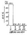
우선, 텔레비젼 전송 선로에서의 에러 비트 특성에 관하여 설명한다. 제1도는 야외 실험에 의해 데이타 신호를 수신할 때의 비교적 임펄스 잡음이 많은 지점에서의 에러 바이트(8비트)중의 에러 비트수 분포의 평균치를 도시하고 있다. 제1도에 도시된 바와 같이 1 비트는 85%를 점유하여 한 비트를 정정하고 두 에러 비트를 검출할 수 있는(단일 에러 수정 및 이중 에러 검출(SEC-DED)이라고 하는 )(8,4) 확대 해밍 코드로는 정정 효과가 한 디지트만큼 이르지 않게 된다.First, the error bit characteristics in the television transmission line will be described. FIG. 1 shows the average value of the distribution of the number of error bits in the error bytes (8 bits) at the point where the relatively high impulse noise when receiving the data signal by the field experiment. As shown in FIG. 1, one bit may occupy 85% to correct one bit and detect two error bits (called single error correction and double error detection (SEC-DED)) (8, 4). With the extended Hamming code, the correction effect does not reach as much as one digit.
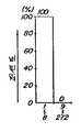
제2도는 송신 신호를 삽입 배열로 한 경우의 수신 데이타의 에러 비트수 분포 평균치의 예를 나타낸 선두이다. 도시된 바와 같이 1 비트 에러는 약 97.1%이다. 이 경우 정정 효과는 2 디지트에 이르지 않는다. 또한, 표준 배열 및 삽입 배열의 어느 것도 효율은 낮아서 단 50%에 이른다. 16 비트 중에서 1 비트를 정정할 수 있고, 2개의 에러 비트를 검출 할 수 있는(SEC-DED)(16,11) 확대 해밍 코드가 사용될 때, 효율은 (8,4) 해밍 코드와 비교해 볼 때 68.7%로 개선되지만 블록 에러율은 개선되지 않는다.2 is a head showing an example of an average number of error bit number distributions of received data when a transmission signal is inserted into an array. As shown, the 1 bit error is about 97.1%. In this case, the correction effect does not reach two digits. In addition, neither the standard arrangement nor the insertion arrangement is low in efficiency, reaching only 50%. When one of the 16 bits can be corrected and two error bits can be detected (SEC-DED) (16, 11) an extended Hamming code is used, the efficiency is compared with the (8, 4) Hamming code. It improves to 68.7% but does not improve block error rate.
한 패킷중의 에러 비트수의 분포에 대해서 조사된다. 제3도는 임펄스 잡음 지역에서 1 비트 내지 8 비트까지의 비트 에러가 99.1%에 이르는 것을 도시한다.The distribution of the number of error bits in a packet is examined. 3 shows that the bit error of 1 to 8 bits reaches 99.1% in the impulse noise region.
파형 왜곡 지역에서 모든 에러 비트는 제4도에 도시된 바와 같이 1 비트 내지 8 비트를 포함한다.All error bits in the waveform distortion area include 1 to 8 bits as shown in FIG.
제5도 및 제6도는 임펄스 지역과 파형 왜곡 지역에서의 에러 버스트 길이(에러 비트수와 무관하게 제1에러 비트에서 최종 에러 비트까지의 비트 길이를 나타냄)의 분포를 도시한다.5 and 6 show the distribution of error burst lengths (representing the bit length from the first error bit to the last error bit, regardless of the number of error bits) in the impulse region and the waveform distortion region.
68 비트 버스트 에러를 정정할 수 있는 코드가 사용해도 한 비트가 개선되면 제5도에 도시된 바와 같이 효율이 약 92(90.8+1.6)%에 이르므로 임펄스 잡음 지역에서는 영향을 받지만, 제6도에 도시된 바와 같이 효율이 약 75(69.0+6.4)% 이므로 한 디지트가 개선되면 파형 왜곡 지역에서는 영향을 받지 않는다.Even if a code that can correct a 68-bit burst error is used, if one bit is improved, the efficiency reaches about 92 (90.8 + 1.6)%, as shown in Figure 5, so that it is affected in the impulse noise region. As shown in Figure 6, the efficiency is about 75 (69.0 + 6.4)%, so an improvement in one digit is not affected in the waveform distortion area.
따라서 단축 삽입 순환 코드와 같은 버스트 에러 정정 코드가 사용될 때 에러 정정에 관한 개선은 기대할 수 없다.Therefore, no improvement on error correction can be expected when a burst error correction code such as a short insert cyclic code is used.
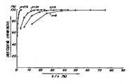
제7도 및 제8도는 각각 전형적인 임펄스 잡음 지역과 파형 왜곡 지역에서의 에러 빈도율에 대한 누진 분포를 도시한다. 제7도 및 제8도에서 변수 b/n(여기서 n은 블록의 길이이며 b는 한 블록중의 에러 비트 수이다)가 사용된다 에러는 긴 블록을 사용하여 정정하는 것이 좋다. 즉, 블록 길이가 제7도에 도시된 바와 같이 8(n=8)일 때 b/n은 0.7, 즉, 모든 에러 블록을 정정하려면 8 비트 중에서 6 비트까지를 정정하지 않으면 안된다. 이것을 실현하는 일은 불가능한 것이다.7 and 8 show the progressive distribution of error frequencies in typical impulse noise regions and waveform distortion regions, respectively. In Figures 7 and 8, the variable b / n (where n is the length of the block and b is the number of error bits in one block) is used. Errors may be corrected using long blocks. That is, when the block length is 8 (n = 8) as shown in FIG. 7, b / n is 0.7, i.e., to correct all error blocks, up to 6 bits of 8 bits must be corrected. It is impossible to realize this.
한편, 블록 길이 n가 272 일때(문자 코드 방송의 경우 1 패킷 길이) 모든 에러는 b/n=0.04로 정정될 수 있다. 제8도에 도시된 바와 같이 모든 에러는 파형 왜곡 영역에서 n=272, b=0.03)으로 정정될 수 있다.On the other hand, when the block length n is 272 (1 packet length in case of character code broadcasting), all errors may be corrected to b / n = 0.04. As shown in FIG. 8, all errors can be corrected to n = 272, b = 0.03 in the waveform distortion region.
이상과 같이, 블록 길이를 가능한한 길게 하여 1 패킷을 1 블럭으로서 정정하는 편이 정정 능력의 점에서 볼 때 유리하며, 실현성도 있음을 알 수 있다.As described above, it is understood that correcting one packet as one block by making the block length as long as possible is advantageous from the standpoint of the correction capability, and it is also feasible.
제1표는 정정 능력, 효율, 알고리즘 용이성, 에러 정정과 검출의 동시 기능, 패킷 신호에 대한 적합성 등을 평가한 전형적인 에러 정정 코드의 4 종류에 대해서 비교한 것이다.The first table compares four types of typical error correction codes for evaluating correction capability, efficiency, algorithm ease, simultaneous function of error correction and detection, suitability for packet signals, and the like.
[제1표][Table 1]

제1표에서 알 수 있는 바와 같이 다수결 논리 코딩회로는 결점이 작기 때문에, 문자 코드 방송의 에러제어에 최고로 적합하다.As can be seen from the first table, the majority vote logic coding circuit has the shortcomings and is therefore most suitable for error control of character code broadcasting.
여러 가지 형태의 다수결 논리 코드가 발견되어 왔지만, 패턴 방식 문자 방송과의 양립성을 생각하면, (1패킷=272비트) 차집합 순환 코드로 된(273,191) 코드를 1비트 단축화한 (272,190) 비트가 일본의 문자 코드 방송에는 최대로 적합하다. 이 코드의 효율 R은 다음과 같다.Although many forms of majority logic code have been found, considering compatibility with pattern-based text broadcasting, (272,190) bits that shorten (273,191) codes of (273,191) with a set-circulation cyclic code (1 packet = 272 bits) It is most suitable for Japanese character code broadcasting. The efficiency R of this code is

에러 정정 능력을 고려해보면, 1패킷중의 8비트 랜덤 에러는 정정될 수 없다. 제3고 및 제4도에 있어서, 임펄스 잡음 지역에서는 99.1%의 에러 정정 효율이 기대되는 반면에 파형 왜곡 지형에서는 100%의 정정 효율이 기대된다.Considering the error correction capability, the 8-bit random error in one packet cannot be corrected. In Figures 3 and 4, 99.1% error correction efficiency is expected in the impulse noise region, while 100% correction efficiency is expected in the waveform distortion topography.
다음, 이 코드에 대한 기본 원리에 관하여 설명한다. 첫째 다수결 논리 디코딩 코드에 관하여 설명한다. 코드 길이가 7이고, 정보 점수 3인 M계열 코드에 관하여 생각한다. 이 코드의 패리티 검사 행렬 H는 다음과 같이 주어진다.Next, the basic principle of this code is explained. First, the majority vote logic decoding code is described. Consider an M series code having a code length of 7 and an information score of 3. The parity check matrix H of this code is given by

e은 잡음은 표시하는 벡터를 나타낸다. 즉,e denotes the vector that noise represents. In other words,
e=(e0,e1,…,e6)e = (e0 , e1 ,…, e6 )
이다. 그리고 신드롬 s는,to be. And syndrome s,
s=eHts = eHt
이며, 여기서 t는 전치를 표시한다. S1,S2및 S1+S3로 구성된 합성 패리티 검사 A1,A2및 A3는 다음과 같다.Where t represents a transpose. Synthetic parity check A1 , A2 and A3 consisting of S1 , S2 and S1 + S3 are as follows.

e0는 A1,A2및 A3모두에 포함되지만 e1내지 e6는 A1,A2및 A3에만 포함된다. 이 경우 A1,A2및 A3는 e0에 대해 직교한다고 말한다.e0 is included in both A1 , A2 and A3 while e1 to e6 are included only in A1 , A2 and A3 . In this case A1 , A2 and A3 are said to be orthogonal to e0 .
e0에 에러가 있는 A1=A2=A3=1이 된다. e1내지 e6가운에 하나에 에러가 있다면 A1,A2및 A3가운에 하나는 1이 된다. 따라서 A1,A2및 A3의 임계치가 2(혹은 3)로 결정되면 다수결 논리 회로의 출력은 에러 비트 e0를 정정할 수 있다. M계열 코드는 순환 코드이므로 상기 작동을 7회 반복하면 7비트중 한 비트가 반드시 정정된다.A, which is an error e01 is a= A 2 = A 3 = 1 . If one in e1 to e6 gowns has an error, one in A1 , A2 and A3 gowns is one. Thus, if the thresholds of A1 , A2 and A3 are determined to be 2 (or 3), then the output of the majority vote logic circuit may correct error bit e0 . Since the M series code is a cyclic code, if the above operation is repeated seven times, one bit of the 7 bits is necessarily corrected.
제9도는 상기 에러 정정 작동을 실행하기 위한 에러 정정 회로예가 도시되고 있다. 또한, 7비트 입력 신호(100)도 도시된다. 신드롬 레지스터(101)의 초기치는 초기에 0으로 세트된다. 입력 신호(100)를 일시적으로 기억시키는 버퍼 레지스터(102)도 도시된다. 입력 신호(100)가 버퍼 레지스터(102)에 완전히 입력될 때까지 동일한 데이타가 신드롬 레지스터(101)에도 로드된다. 이때까지 다수결 논리 회로(109)는 동작되지 않는다. 도면번호(103) 내지 (107)는 2모듈(modulo) 가산기를 나타낸다.9 shows an example of an error correction circuit for performing the error correction operation. Also shown is a 7 bit
7비트의 보든 데이타가 가산기와 레지스터(101)(102)로 완전히 입력되는 시점에서 에러 정정 작동이 시작된다. 즉, 다수결 논리 회로(109)가 동작을 개시한다. 세 입력(111),(112),(113)이 다수결 논리 회로(109)에 인가된다. 이러한 세 입력 가운데 두 입력 또는 세 입력이 1이면, 처음에는 다수결 논리 회로(109)로부터의 출력(114)이 1이 되고 가산기(107)에서 에러 비트를 정정한다.The error correction operation starts when all seven bits of data are completely input into the adder and the
이것과 동시에 에러 비트로 인하여 신드롬에 미치는 역 효과를 제거하기 위해, 신드롬 레지스터(101)의 수정을 출력(114)에 의해 행해진다. 이 작동에 의해 에러 정정이 완전히 바르게 정정되는지 안되는지를 판정하는 것이다. 즉, 모든 비트 정정 작동이 종료시에 모든 에러가 정정되면, 신드롬 레지스터(101)의 내용은 모두 0이 된다. 신드롬 레지스터에서의 내용이 0이 아니면 정확하게 정정되지 않았다고 판정된다. 이 경우 생성 다항식은 다음과 같다.At the same time, in order to eliminate the adverse effects on the syndrome due to error bits, modification of the syndrome register 101 is done by the output 114. By this operation, it is determined whether or not error correction is completely corrected. That is, if all errors are corrected at the end of all bit correction operations, the contents of the syndrome register 101 are all zeros. If the contents in the syndrome register are not zero, it is determined that the correction is not correct. In this case, the generated polynomial is

버퍼 레지스터(102)의 선두 비트에 에러가 발생되고 그 다음 정정 동작을 행하는 시점에서는 이 정정 비트는 X7비트이다. 따라서 X7비트로 인해 신드롬 레지스터에 미치는 효과는 다음과 같다.At the time when an error occurs in the first bit of the

여기서 { }기호는 잉여 집합을 나타낸다. 따라서 출력(114)에 응답하여 신드롬 수정 비트가 필요하다.Where the {} symbol represents a surplus set. Thus, a syndrome modification bit is needed in response to the output 114.
다음에는 데이타를 실제 전송하는 경우의 예를 설명한다. 생성 행렬은 다음과 같다.Next, an example of the actual data transmission will be described. The generation matrix is

3비트 정보 001에 응답하여 코드 C는 다음과 같이 주어진다.In response to the 3-bit information 001, the code C is given as follows.

이 코드가 에러 없이 전송될 때, 수신측에서의 신드롬 내용은 당연히 0000이 된다. 신드롬 레지스터(101)의 비트 변화를 다룬다.When this code is transmitted without error, the syndrome content at the receiving end is naturally 0000. It handles bit changes in the syndrome register 101.
0100 제1, 제2, 제3 및 제4비트가 로드0100 First, second, third and fourth bits are loaded
1010 제1 내지 제5비트가 로드1010 first to fifth bits are loaded
1101 제1 내지 제6비트가 로드1101 first to sixth bits are loaded
0000 제1 내지 제7비트가 로드0000 First to seventh bits are loaded
상기된 바와 같이 신드롬 레지스터(101)의 내용은 0000이 되며 따라서 모든 정보는 어떠한 에러도 없이 출력단자(110)으로부터 출력된다.As described above, the content of the syndrome register 101 is 0000, so that all information is output from the
다음에는 제2비트에 에러가 있는 경우를 검사하자. 이 경우 수신된 데이타는 0110111이다. 따라서 신드롬 s(x)는 다음과 같다.Next, examine the case where there is an error in the second bit. In this case, the received data is 0110111. Therefore, the syndrome s (x) is

신드롬 레지스터(101)의 내용은 0111이다. 에러 정정 작동을 조사해 보면 다음과 같다.The contents of the syndrome register 101 are 0111. The error correction behavior is as follows.

따라서 제2비트째의 에러는 정정될 수 있다.Therefore, the error of the second bit can be corrected.
다음에는 본 발명이 (273,191) 다수결 논리 디코딩 코드를 선택하는 이유에 관하여 설명한다. 종래의 다수결 논리 디코딩 코드는 최장 순차 코드, 해밍 코드, 유클리드 기하학 코드, 최종 사영 기하학 코드 및 차집합 순환 코드 등이다. 이러한 코드에서 최장 계열 코드, 해밍 코드 및 유클리드 기하학 코드는 2-1의 형태로 되면 1패킷을 1블럭으로 만들기 위하여 m은 9,n은 511로 하고 n이 272가 될 때까지 239 비트가 감축되어야 한다. 그러나 전송 효율은 이러한 비트 감축으로 인해 현저하게 감소된다. 최종 사영 기하학 코드의 경우에 있어서 n은 (2m-1)/(2S-1)로 구해질 수 있다. 그러나 한 패킷중에서 8비트 이상의 에러 비트가 정정되고, 효율이 190/272이상이 구해질 수 있다.The following describes why the present invention selects the (273,191) majority vote logical decoding code. Conventional majority vote logic decoding codes are the longest sequential code, hamming code, Euclidean geometry code, final projected geometry code, subset cyclic code, and the like. In these codes, the longest series code, Hamming code, and Euclidean geometry code should be 2-1 and 239 bits should be reduced until m is 9,
(273,191) 다수결 논리 디코딩 코드는 차집합 순환 코드에서 구해질 수 있는데, 0,18,24,46,50,64,103,112,115,126,128,159,166,167,186,196,201의 모든 정수의 서로간의 차가 서로 다르다. 이 코드의 생성 다항식은 다음과 같이 구해진다.The majority vote logical decoding code can be obtained from the set cyclic code, where the difference between all integers of 0, 18, 24, 46, 50, 64, 103, 112, 115, 126, 128, 159, 166, 167, 186, 196, 201 is different from each other. The generated polynomial of this code is given by

다수결 논리 회로에 인가된 입력 A1내지 A17은 다음과 같다.Inputs A1 to A17 applied to the majority vote logic circuit are as follows.

다음에 제10도는 송신 설비에 장치되는 신호 송신 회로를 도시한다. 190비트로 구성된 정보 비트(200)는 1비트를 감소시킴으로써 원래의 코드로부터 유도된다. 따라서 정보 부분은 190비트를 포함한다. 82비트의 패리티 레지스터(201)의 초기치는 0으로 되며, 스위치(202),(203),(204)는 초기에 실선으로 표시된 부분으로 이동된다. 정보 비트(200)는 스위치(204)를 통해 전송되고 전송된 패킷 신호(205)로 된다. 이것과 동시에 정보 비트(200)은 스위치(202),(203)와 가산기(206)을 통해 전송되고, 이에 의해 패리티 비트는 식(1)에 따라 발생된다. 모든 정보 비트(200)가 전송된 후 패리티 레지스터(201)의 내용은 패리티 비트로 전송된다. 따라서 이 시간점에서부터 스위치(202),(203),(204)는 파선으로 나타내진 바와 같은 위치로 이동되어 패리티 레지스터(210)에 있는 내용이나 신호는 전송된 패킷 신호(205)로서 유도된다.10 shows a signal transmission circuit installed in a transmission facility. An information bit 200 consisting of 190 bits is derived from the original code by reducing one bit. Thus the information portion contains 190 bits. The initial value of the 82-
제11도는 본 발명에 따른 디코딩 회로를 도시한다. 입력 신호(300)(즉, 수신된 신호)의 에러는 정정되어야만 한다. 비트 0는 이 입력 신호의 선단 즉, 전송된 신호가 부가될 때 단축된 한 비트에 부가된다. 따라서 입력 신호는 273비트를 포함한다. 이러한 사실을 제외하면 이 구조는 제9도에 도시된 구조의 원리와 실제로 유사하다. 정정되어야 할 데이타를 기억시키기 위한 데이타 레지스터(301)는 273비트를 보유할 수 있다. 신드롬 레지스터(302)는 82비트의 시프트 레지스터로 구성된다. 모듈로 2가산기(303),(323)는 다수결 논리회로(341)에 인가되는 입력 신호를 발생시킨다. 가산기(307) 내지 (323)의 입력수는 신드롬 레지스터(302)의 레지스터수를 나타낸다. 예를 들면 가산기(307)의 입력(5),(10)은 신드롬 레지스터(302)의 레지스터단, S5,S10의 각 출력 S5,S10을 나타낸다. 모듈로 2가산기(307) 내지 (323)로부터의 출력 (324) 내지 (340)은 다수결 논리회로(341)에 인가되고, 다수결 논리회로(341)로부터의 정정 신호(342) 및 레지스터(301)로부터의 출력 신호는 모듈로 2가산기(343)에 인가된다.11 shows a decoding circuit according to the invention. Errors in the input signal 300 (ie, received signals) must be corrected.
신드롬 레지스터(302)의 초기치는 S0=0,…,S81=0으로 세트된다. 입력 신호(300)의 모드 비트는 데이타 레지스터(301)에 기록될 때까지 다수결 논리회로(341)는 동작하지 않는다. 모든 데이타가 데이타 레지스터(301)로 입력된 후 제1신드롬은 레지스터단(S0내지 S81)에 의해 설정되며, 다수결 논리회로(341)는 임계치 9(혹은 10)에서 동작하여 선두 비트 에러는 정정된다. 신드롬 계산을 1비트씩 앞으로 진행될 때마다 에러 정정과 데이타 레지스터(301)의 내용은 1비트씩 이동된다. 가산기(343)에서는 정정 신호(342)에 응답하여 레지스터(301)의 출력을 정정하며, 이에 의해 정정된 데이타(344)를 출력한다.The initial value of the
상기 디코딩 회로는 디코딩 절차의 개요를 도시한다. 제12도는 문자 코드 방송을 실제로 수신하는데 사용될 수 있는 회로를 도시한다. 제12도에는 CPU버스 라인(400), CPU(도시 안됨)로부터의 16비트 출력 포트(401), 궤환 기능을 갖춘 82비트 신드롬 레지스터(403), 데이타 레지스터(404), 17개의 다수결 논리 회로를 갖춘 다수결 논리 회로(405), 16비트 병렬-직렬 변환기(406), 16비트 직렬-병렬 변환기(407), 16비트 펄스 발생기(408), 데이타 로드 및 데이타 정정 신호 발생용 로드 및 정정 게이트 발생기(409), 게이트(410), 준비 신호 발생기(411), 에러 상태 레지스터(412), 16비트 병렬 입력 데이타(413), 16비트 병렬 출력 데이타(414), 시작 신호(415), 로드 신호(416), 정정 명령 신호(417), 로드 종료 신호(418), 클럭 신호(419), 직렬 입력 데이타(420), 직렬 출력 데이타(421), 16비트 클럭 신호(422), 82비트 신드롬 데이타(423), 에러 정정 신호(424), 에러 상태 신호(425), 준비 신호(426), 16비트 반송 신호(427)가 포함된다.The decoding circuit shows an overview of the decoding procedure. 12 shows circuitry that can be used to actually receive a character code broadcast. 12 shows a
신드롬 레지스터(403)는 CPU에서 전송된 시작 신호에 응답하여 클리어되고 로드 및 정정 게이트 발생기(409)는 로드 게이트 신호(428)가 발생되도록 제어된다. 신드롬 레지스터(403)의 입력 신호는 이 신호에 응답하여 신드롬 레지스터(403)에 연속적으로 로드된다. 그런 다음 CPU는 16비트 데이타를 출력 포트(401)에 전송하여 로드 신호(416)가 발생하게 된다. 16비트 펄스 발생기(408)는 로드 신호(416)에 응답하여 시프트 작동을 위한 16비트 클럭 신호를 발생시켜 병렬-직렬 변환기(406)의 데이타가 판독되고 신드롬 레지스터(403) 및 데이타 레지스터(404)에 로드된다. 16비트 클럭 신호는 클럭 신호(419)에 응답하여 발생된다. 만약 이 신호가 5MHz 이상의 주파수를 갖는 신호라면 한 패킷에서의 에러는 1ms 이하의 시간내에 정정될 수 있다. 준비 신호 발생기(411)는 로드 신호에 응답하여 리세트되고 교신 상태로 된다. 16 비트 시프트 클럭의 전송이 종료되자마자 16비트 반송 신호(427)가 발생되어 준비 신호 발생기(411)가 준비 상태로 된다. 다음 명령은 준비 신호(426)에 응답하여 CPU에 명령 요구된다. 상기 작동은 한 패킷인 272 비트동안 반복된다. 따라서 데이타 세트는 272/17회 반복되며 로드 명령은 17회 파생된다.The
모든 데이타가 병렬-직렬 변환기(406)에 세트되고 로드 명령이 발생될 때 CPU는 로드 종료 신호(418)를 발생시켜 신드롬 레지스터(403)가 1비트만큼 이동된다. 이 1비트는 단축된 1비트와 동일하다. 그 다음 에러 정정이 선두 비트에서부터 실행된다. 에러 정정은 16비트 각각에 대해 실행되며 에러 정정된 16비트의 데이타는 CPU에서 판독된다. 정정 신호(417)는 CPU로부터 유도된 정정 신호이며, 한 에러 정정 명령에 응답하여 데이타 레지스터(404)의 선단에 있는 16비트 데이타의 에러가 정정된다. 로드 신호(416)에 의해 발생되는 로드 명령의 경우에 있어서와 같이, 에러 정정 신호(417)에 응답하여 16비트 클럭 신호가 16비트 펄스 발생기(408)에서 로드 신호가 출력되어 레지스터(403),(404)는 16비트만큼 이동시킨다. 데이타 레지스터(404)의 선두가 에러인 것으로 검출될 때 에러 정정 신호(417)에 응답하여 에러 비트가 반전되고 이 비트는 직렬-병렬 변환기(407)에 순차 로드된다.When all data is set in the parallel-to-
에러 정정 신호(424)는 다수결 논리회로(405)에서 출력되며, 정정 신호(417)에 의해 제어되어 로드 및 정정 게이트 발생기(409)로부터의 출력 신호에 의해 제어된다. 데이타 로드의 경우에 있어서와 같이, 16비트의 에러 정정이 종료된 시점에서, 준비 신호(426)에 의해서 CPU에 16비트분의 에러 정정이 끝나고, 직렬-병렬 변화기로서의 레지스터(407)에 데이타가 로드되어 있는 것을 알 수 있다. 이러한 동작을 17회 반복하면 패리티를 포함하는 에러 정정후의 272비트 데이타를 디코드할 수 있다.The error correction signal 424 is output from the majority
에러 상태 레지스터(412)는 신드롬 레지스터(403)로부터 82비트가 인가되는 OR게이트를 포함한다. 신드롬 레지스터(403)의 내용이 모두 0인지 아닌지가 검사된다. 이러한 상태에서 에러 상태 신호(425)가 CPU에 인가될 때 정확하게 정정되었는지 아닌지 판정될 수 있다. 즉, 신드롬 레지스터의 내용이 모두 0일때에만 정확한 정정이 실행될 것이다.The error status register 412 includes an OR gate to which 82 bits are applied from the
이제까지는 각각의 16비트 데이타가 로드되는 것에 대해 기술하였으며, 각각의 16비트 데이타가 정정된 후 이 데이타가 CPU에 의해 판독되는 것에 대해 기술되었지만 원리적으로 각각 8비트, 34비트, 64비트 혹은 136비트 데이타도 상기된 바와 유사한 방식으로 처리될 수 있다. 종래의 하드웨어 규모에서는 16비트 정도가 적당하다. 한 명령이 여러 비트로 구성되면 회로 성분(401),(402),(406),(407)은 커지고 복잡해진다.So far it has been described that each 16-bit data is loaded and that this data is read by the CPU after each 16-bit data has been corrected, but in principle 8-bit, 34-bit, 64-bit or 136 respectively. Bit data can also be processed in a similar manner as described above. On the conventional hardware scale, 16 bits are suitable. If a command consists of several bits, the
다수결 논리 디코딩 코드에 있어서, 다수결 논리 소자의 수가 증가되면 실제로 사용되는 논리 회로의 수는 지수 함수적으로 증가될 것이다. 따라서 다수결 논리 회로의 수가 17인 코드는 실제로 사용되지 않는다. 이와같은 논리 회로를 제공하기 위하여 논리 OR 입력의 수는
따라서, 본 발명에 따르면 17개의 다수결 입력(다수결 논리 소자) 논리는 제13도에 도시된 바와같은 가장 단순한 논리 소자를 이용하여 실행될 수 있다.Thus, according to the present invention, the 17 majority vote input (multiple logic logic) logic can be executed using the simplest logic element as shown in FIG.
제13도에서 각각 8개의 다수결 논리 소자(500),(501)가 도시된다. 나머지의 한 다수결 논리 소자(502)도 도시된다. 또한 제13도에는 4×256비트 ROM(503),(504), 각각의 ROM(503),(504)로부터의 4비트 출력(505),(506)과 출력(508)을 갖춘 종래의 가산기(507)도 도시된다. 또한 이 도면에는 비교기(509), 비교기(509)의 B측에 인가되는 입력(510)과 비교기(509)로부터의 A>B인 출력(511)도 도시된다.In FIG. 13, eight majority
8비트 입력(500)은 ROM(503)의해서 그것의 1의 수를 4비트 표시의 출력(505)으로서 출력한다. 예를들어 M0이 1이고 M1=M2=M3=M4=M5=M6=M7이 0이면, 출력(505)은 1000으로서 1을 나타낸다. 이러한 방식으로 또다른 8비트 입력(501)이 ROM(504)에 의해 처리되어 1을 나타내는 출력(506)이 유도된다. 가산기(507)는 2진 출력(507),(506)과 캐리인 제17다수결 논리 소자M16을 더하여 출력(508)이 유도된다. B측 8비트 입력(500)은 ROM(503)의해서 그것의 1의 수를 4비트 표시의 출력(505)으로서 출력한다. 예를들어 M0이 1이고 M1=M2=M3=M4=M5=M6=M7이 0이면, 출력(505)은 1000으로서 1을 나타낸다. 이러한 방식으로 또다른 8비트 입력(501)이 ROM(504)에 의해 처리되어 1을 나타내는 출력(506)이 유도된다. 가산기(507)는 2진 출력(507),(506)과 캐리인 제17다수결 논리 소자 M16를 더하여 출력(508)이 유도된다. B측의 입력이 8로 제한되고 A측의 입력(508)이 입력(510)보다 클때에만 A>B인 출력(511)이 1로 유도된다. 따라서, 9 이상이 17개이 입력에 입력될 때 다수결 논리가 검출된다.The 8-
지금까지는 본 발명에 따른 문자 코드 방송용 에러 정정 방법과 실제의 수신 논리 회로 구성에 사용되도록 채택된(272,190) 다수결 논리 디코딩 코드의 기본 원리를 설명하였다. 실제로 신호를 송신할 경우 82비트 패리티 신호나 190비트 정보 신호만이 송신을 위해 반전되어야 하며 수신될 때 기억되어야 한다. 그 이유는 한 패킷내의 신호가 모두 0일 때 이 신호는 어떠한 코드도 표시하지 않기 때문이다.So far, the basic principles of the majority decision logic decoding code (272,190) adopted for use in the error correction method for character code broadcasting and the actual reception logic circuit according to the present invention have been described. When actually transmitting a signal, only 82-bit parity signals or 190-bit information signals should be inverted for transmission and stored when received. The reason is that when the signals in a packet are all zero, this signal does not indicate any code.
이제까지의 방법은 패킷 신호가 CPU내의 RAM에 입력되고 RAM의 데이타가 에러 제어 입출력으로 전송되어 에러 정정된 데이타가 다시 판독되게 하기 위한 것이지만 데이타를 CPU의 RAM에 입력시키기 전에 에러가 정정된다. 이 경우 에러 정정 시간은 데이타를 시프트 레지스터에 로드시키는데 필요한 시간과 실제로 동일하다. 그 결과로 상기 형태로 구성된 둘 이상의 에러 정정 회로가 필요하다.Until now, the packet signal is input to the RAM in the CPU and the data in the RAM is transmitted to the error control input and output so that the error corrected data is read again, but the error is corrected before the data is input to the RAM of the CPU. In this case the error correction time is actually equal to the time required to load the data into the shift register. As a result, more than one error correction circuit configured in the above form is needed.
상기에러 정정 방법은 텔레비젼 전송 선로의 비트 에러 특성에 적합하다. 이 방법에 따르면 매우 효율적인 에러 정정 능력이 구해질 수 있다. 더 나아가 다른 모든 에러 정정 방법보다 간단한 단순 디코딩 회로에 의해 272비트가 완전히 정정될 수 있다. 결과적으로 본 발명에 따른 에러 정정 방법은 값싼 하드웨어를 필요로 하는 가정용 텔레비젼 수상기의 에러 정정 회로에 적합한 것이다. 또한, 본 발명에 의한 방법은 에러를 동시에 정정하고 검출하여 에러 코드를 표시할 수 없는 문자 코드 방송 시스템에 이용하기 가장 적합하다.The error correction method is suitable for the bit error characteristics of the television transmission line. According to this method, a very efficient error correction capability can be obtained. Furthermore, 272 bits can be completely corrected by a simple decoding circuit, which is simpler than all other error correction methods. As a result, the error correction method according to the present invention is suitable for an error correction circuit of a home television receiver requiring cheap hardware. In addition, the method according to the present invention is most suitable for use in a character code broadcasting system that cannot simultaneously correct and detect errors and display error codes.
본 발명에 따른 방법은 이미 패턴 방식 문자 방송으로서 전파 기술 심의회로부터 회답되온 방식과 같은 TV 신호의 1주사선당 272비트의 디지털 신호를 전송하는 방식이기 때문에, 장래는 문자 코드 방송 이외에 팩시밀리용 디지털 팩스, 컴퓨터 스프트웨어를 전송하는 스프트웨어 방송, 맹인을 위한 점자 방송 등 그밖의 코드 방송을 실시하는 것과 함께, 비트율이 같으면, 모두 같은 방식으로 정정이 가능하다.Since the method according to the present invention is a method of transmitting a digital signal of 272 bits per scan line of a TV signal, such as a method already returned from the radio technology council as a pattern-based text broadcasting, in the future, in addition to text code broadcasting, in the case of digital fax for facsimile, In addition to performing other code broadcasting such as software broadcasting for transmitting computer software, braille broadcasting for the blind, and all of the same bit rates, correction can be performed in the same manner.
상기된 바와같이(272,190) 다수결 논리 디코딩 코드는 1패킷내의 어떤 위치에서도 일어날 수 있는 9비트 이하의 어떠한 에러도 정정할 수 있다. 그러나 9비트 이상의 에러를 정정할 경우에는 소량의 에러 정정 패턴만이 실재하며 실제로 8비트 이상의 거의 모든 에러를 정정하는 것은 불가능하다.As discussed above (272, 190), the majority vote logical decoding code can correct for any error of nine bits or less that may occur at any location within one packet. However, when correcting an error of 9 bits or more, only a small amount of error correction patterns exist, and it is impossible to correct almost all errors of 8 bits or more.
따라서 비교적 높은 정확도를 갖춘 약 9,10,11,12비트 가량의 에러를 정정할 수 있는 본 발명에 따른 또 다른 실시예를 기술한다.Therefore, another embodiment according to the present invention that can correct about 9, 10, 11, 12 bits of error with relatively high accuracy is described.
다음 실시예에 있어서, 거의 모든 9비트 에러 패턴은 완전히 정정되어 화면 에러율이 상당히 개선되게 된다.In the following embodiment, almost all 9 bit error patterns are completely corrected so that the screen error rate is significantly improved.
우선 기본 원리에 대해 기술해보면, 상기된 바와같이(272,191) 코드 생성 다항식G(X)은 다음과 같다.First, the basic principle will be described. As described above (272, 191), the code generation polynomial G (X) is as follows.

발생기 다항식의 행렬식은 다음과 같다.The determinant of the generator polynomial is

단, I는 191×191 단위의 행렬을 나타내며, P는 82×191로 된 행렬을 나타낸다. 검사 행렬 H는 다음과 같다.However, I represents a matrix of 191 × 191 unit, and P represents a matrix of 82 × 191. The check matrix H is

행렬 H의 82행의 벡터의 선형 결합에 의해 각각의 비트상에서 직교하도록한 디코드 검사 행렬을 구상하는 것이 가능하다. 17개의 검사식의 선두 부분은 다음과 같이 표시된다.By linear combination of the 82 rows of the matrix H, it is possible to design a decode check matrix that is orthogonal on each bit. The head of the 17 test expressions is represented as follows.

여기서 H1은 검사 행렬 H의 선형 변환에 의해 구해진 직교 패리티 검사합이다.Where H1 is an orthogonal parity check sum obtained by linear transformation of the check matrix H.
수신 벡터 r은 다음과 같다.The reception vector r is

여기서 c는 코드 신호이고, e는 에러 신호이다. 따라서 직교 패리티 검사합은 다음과 같다.Where c is a code signal and e is an error signal. Therefore, the orthogonal parity check sum is as follows.

따라서 에러가 8비트 이상이면 에러만을 고려하여 eH1만이 조사될 필요가 있다. 에러가 9비트 이하이면 모든 에러는 코드의 기본 원리의 관점에서 정정될 수 있다.Therefore, if the error is 8 bits or more, only eH1 needs to be examined considering only the error. If the error is 9 bits or less, all errors can be corrected in terms of the basic principles of the code.
첫째로 처음 9비트가 모두 에러이면 에러 벡터 e는 다음과 같이 표시된다.First, if the first 9 bits are all errors, the error vector e is represented as

즉,In other words,

이다. 1의 수는 11개인데 이것은 임계치가 9여서 제1비트가 정정된다는 것을 나타낸다. 나머지 8비트는 정정될 수 있어서 결국 9비트 모두 정정될 수 있다.to be. The number of ones is eleven, indicating that the threshold is nine so that the first bit is corrected. The remaining 8 bits can be corrected so that all 9 bits can be corrected.
따라서 9비트 에러의 경우 정정 작용이 일어나기전에 선두 에러가 검출된 후 정정되면 나머지 8개의 에러비트도 정정될 수 있다. 따라서 9개의 에러 비트는 정정될 수 있다. 에러 정정이 제1에러 정정 작동으로 불가능하면 데이타는 1비트 가량 순환 이동되어 에러 정정 작동이 다시 실시된다. 데이타가 순환 이동될 동안 선두 에러 비트가 검출되어 9개의 에러 비트가 모두 정정될 수 있다.Therefore, in the case of 9-bit error, if the leading error is detected and corrected before the corrective action occurs, the remaining eight error bits may be corrected. Thus, nine error bits can be corrected. If error correction is not possible with the first error correction operation, the data is cyclically shifted by one bit and the error correction operation is performed again. The leading error bit can be detected while the data is circularly shifted so that all nine error bits can be corrected.
둘째로, 아래의 10비트 에러에 대해 생각해 보기로 하자.Second, consider the following 10-bit error.

1의 개수는 10개가 되기 때문에, 선두 비트를 정정한다. 나머지 9개의 에러는 (1)항에서 설명한 바와같이 정정할 수 있기 때문에, 이와같은 모양의 10개의 에러는 정정할 수 있다.Since the number of 1s is ten, the first bit is corrected. Since the remaining nine errors can be corrected as described in paragraph (1), the ten errors of such a shape can be corrected.
셋째로, 처음 11비트가 모두 에러일때에는 다음과 같다.Third, if all of the first 11 bits are errors,

1의 수가 9개이므로 선두 비트가 정정된다. 나머지 10개의 에러 비트는 둘째번 예에 기술된 바와같이 정정될 수 있다. 따라서 상기의 에러 형태는 완전히 정정될 수 있다.Since the number of ones is nine, the first bit is corrected. The remaining ten error bits can be corrected as described in the second example. Thus, the above error pattern can be completely corrected.
넷째로, 처음 12비트가 모두 에러일 경우에는 다음과 같다.Fourth, if the first 12 bits are all errors,

1의 수가 8이므로 선두 비트가 에러일 경우에도 에러는 정정될 수 없다. 즉, 정확하게 정정될 수 없다.Since the number of 1s is 8, the error cannot be corrected even when the first bit is an error. That is, it cannot be corrected correctly.
다섯째로, 11개의 연속 비트가 모두 에러이고 이 에러가 제2비트에서부터 시작된다고 생각하자.Fifth, suppose all 11 consecutive bits are errors and this error starts with the second bit.
이 경우에는 다음과 같다.In this case,

여기에는 1이 9개 있으므로 선두 비트가 정확하다 하더라도 선두 비트는 정정될 수 있다. 따라서 최종 비트까지 정정이 된다 하더라도 정확하게 정정되지 않는다. 정확하게 정정되지 않는다는 것은 모두가 0은 아닌 신드롬 레지스터의 내용에 의해 검출된다.Since there are nine 1s, the first bit can be corrected even if the first bit is correct. Therefore, even if the last bit is corrected, it is not corrected correctly. Not corrected correctly is all detected by the contents of the non-zero syndrome register.
이 경우에 있어서 데이타는 1비트만큼 순환이동되어 에러 데이타는 세 번째 예에 기술된 바와같은 에러 데이타와 동일한 형태를 구비하게 된다. 결국 에러 정정이 실행될 수 있다.In this case, the data is cyclically shifted by one bit so that the error data has the same form as the error data as described in the third example. Eventually error correction can be performed.
273비트의 제1비트가 직교되도록 직교 패리티 검사합 H1이 구성되는 것에 대해 기술되었으며, 차집합 원리는 적용함으로써 제2비트가 직교하는 행렬이 구성될 수 있다. 이 경우에 실제 회로와 연관하여 기술된 로드 종료 명령(단축된 비트를 1비트 시프트시킴)은 필요없다. 따라서 에러 정정은 제2비트에서부터 실행되어 회로의 구성이 단순화될 수 있다.The orthogonal parity check sum H1 is configured such that the first bit of 273 bits is orthogonal, and by applying the difference principle, a matrix in which the second bit is orthogonal can be configured. In this case, the load termination instruction (shifting the shortened bit by 1 bit) described in association with the actual circuit is not necessary. Therefore, error correction is performed from the second bit so that the configuration of the circuit can be simplified.
상기된 바와같이 에러 비트 집단의 선두 비트가 가능한한 빨리 정정되면 잔여 에러 비트는 높은 정정율로 정정된다.As described above, if the first bit of the group of error bits is corrected as soon as possible, the remaining error bits are corrected at a high correction rate.
따라서 첫 번째 예에 기술된 바와같이 8비트 이상의 에러 정정 확율은 순환 코드의 순환 특성을 이용하는 동안 제1에러 정정 작동 후 완전 정정이 불가능한 것으로 판정될때 수신된 데이타를 1비트 이동시킴으로써 증가된다.Thus, as described in the first example, the error correction probability of 8 bits or more is increased by shifting the received data one bit when it is determined that full correction is impossible after the first error correction operation while using the cyclic characteristics of the cyclic code.
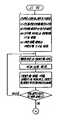
제14도는 에러 정정 작동에 대한 플로우챠트의 예를 도시한다.14 shows an example of a flowchart for the error correction operation.
제15도는 본 발명의 제2실시예를 실행하기 위한 실제 하드웨어를 도시한다. 제15도에는 CPU(도시 안됨) 버스 라인(600), CPU 출력 포트(601), CPU 입력 포트(602), 병렬-직렬 변환기(603), 직렬-병렬 변환기(604), 게이트(605),(506), 모듈로 2가산기(607),(637), 데이타 레지스터(608), 신드롬 레지스터(609), 타이밍 발생기(610), 에러 상태 레지스터(611), 다수결 논리 회로(612), 시작 명령 신호(613), 클리어 신호(614), 로드 명령 신호(615), 로드 게이트 신호(616), 로드 클럭 신호(617), 정정 게이트 신호(618), 정정 클럭 신호(619), 에러 상태 신호(620), 82비트 신드롬 신호(621), 에러 정정 신호(622), 정정 종료 신호(623), 페치 명령 신호(624), 페치 준비 신호(625), 페치 클럭 신호(626), 로드 데이타(627), 페치 데이타(628), 로드 직렬 데이타(629), 순환된 로드 데이타(630), 신드롬을 구하고 데이타를 재배열시키기 위한 로드 데이타(631), 시프트된 원래 데이타값을 보유하기 위한 데이타 레지스터(632), 에러 정정된 데이타(633), 1비트 시프트된 재배열된 데이타(634), 데이타 시프트 클럭 신호(635)와 병렬 로드 신호(636)가 있다.Figure 15 shows actual hardware for implementing the second embodiment of the present invention. 15 shows a CPU (not shown)
다음에는 이 회로의 작동에 대해 기술된다. 작동 모드는 첫째, 초기 데이타가 CPU로부터 로드되는 로드 모드와 둘째, 정정이 실시되는 정정 모드와 셋째, 에러 정정후 데이타가 CPU에 의해 판독되는 페치 모드로 구분된다.The following describes the operation of this circuit. The operation modes are divided into first, a load mode in which initial data is loaded from the CPU, second, a correction mode in which correction is performed, and third, a fetch mode in which data is read by the CPU after error correction.
첫째, 로드 모드에 대해 기술하면 다음과 간다. 272비트로 구성된 1패킷 신호에 응답하여 CPU는 시작명령(631)을 출력시키고 리세트 신호(614)에 응답하여 신드롬 레지스터(609)의 82까지 상태는 모두 0으로 세트된다. 그 다음 CPU는 데이타가 출력 포트에 로드되도록 세트되어 로드 명령 신호(615)가 발생된다. 병렬 데이타는 레지스터(603)에 로드된다. 로드 제어 신호(616)에 응답하여 게이트(605),(606)가 제어되어 입력 신호(629)는 신드롬 레지스터(609)와 데이타 레지스터(632)에 순차적으로 로드된다. 한 패킷 신호는 272비트로 구성되고 단축된 제1비트의 내용은 0으로 세트된다. 병렬 데이타는 8비트와 16비트로 구성된 단위 신호의 형태로 병렬-직렬 변환기(630)에 인가된다. 따라서 로드 작동은 35회나 18회 반복된다. 데이타를 신드롬 레지스터(609)와 로드 데이타 레지스터(632)에 로드시키는 것이 종료되면 레지스터(632)내의 모든 데이타는 병렬 로드 신호(636)의 타이밍에서 데이타 레지스터(608)에 복사된다. 이 단계에서 에러 정정 신호(622)는 정정 게이트 신호(618)에 응답하여 당연히 발생되지 않는다.First, the description of the load mode goes as follows. In response to the one-packet signal composed of 272 bits, the CPU outputs a
둘째 정정 모드에 대해 설명한다. CPU로부터 데이타를 로드시키는 작동을 끝마치자 마자 정정 모드가 시작된다. 정정 클럭 신호(619)는 273비트에 대해 연속적으로 출력된다. 여기서 제1비트가 단축되어 정정 게이트 신호(618)의 기간은 272비트와 동일한 기간을 갖추고 있다. 에러 정정 신호가 다수결 논리 회로(612)로부터 출력될 때 데이타 레지스터(608)에 있는 데이타와 신드롬 레지스터(609)에 있는 신드롬은 에러 정정 신호(622)에 응답하여 정정된다. 따라서 에러 정정은 수신된 패킷 신호의 비트 순으로 완성된다.The second correction mode will be described. As soon as you finish loading the data from the CPU, correction mode begins. The
신드롬 레지스터(609)에 있는 82비트가 에러 상태 레지스터(611)에 의해 모두 0으로 검출되지 않으면 회로는 다음 단계로 진행한다. 이것은 에러 상태 레지스터 신호(620)에 의해 시작된다. 첫째, 데이타 레지스터(632)의 원래 데이타는 1비트만큼 순환 이동된다. 시프트 클럭 신호(635)의 비트수는 1비트 시프트와, 신드롬을 구하기 위한 시프트 수의 합이며 즉, 전체 비트수는 274비트이다. 이 출력 신호는 게이트(605),(606)를 통하여 신드롬 레지스터(609)로 연속적으로 로드되어 신드롬이 발생된다. 이 경우에 비트 위치를 바꾸기 위해 1비트가 제거되므로 클럭 신호(619)는 273비트로 구성된다. 데이타 레지스터(632)의 데이타가 274비트에 대해 이동될 때 신드롬이 발생된다. 이때 로드 데이타 레지스터(632)의 273비트는 병렬 로드 신호에 응답하여 데이타 레지스터(608)에 로드된다. 그 다음에 상기 에러 정정 작동이 실행된다. 그러나 단축된 최종 비트는 정정되지 않는다.If the 82 bits in the
셋째, 페치 모드에 대해 설명한다. 에러 상태 신호(620)가 에러가 없음을 나타내지 않으면 상기 작동 순서가 자동 반복된다. 에러 정정 작동은 처음 정정되어야할 선두 비트를 1비트 이동시킴으로써 제73회 반복된다. 이러한 작동후 원래 상태와 동일한 상태가 얻어지므로 에러 정정 종료 신호(623)가 CPU로 전달된다. 에러 상태 신호(620)는 CPU에서 판독된다. 모든 에러가 완전히 정정되지 않으면 정정이 잘못되므로 에러 상태가 검출된다.Third, the fetch mode will be described. If the
정확히 정정될 때 CPU는 페치 명령 신호(624)를 발생시키며 데이타 레지스터(608)에 기억된 신호가 사용된다. 더 나아가 선두 비트가 불필요하게 되어 273비트중 272비트가 페치된다. 이 데이타는 데이타 레지스터(607)에서 직렬-병렬 변환기(604)로 연속적으로 로드된다. CPU는 페치 명령 신호(625)에 응답하여 직렬-병렬 변환기(604)로부터의 신호를 수신하여 다음 페치 명령(624)이 발생하게 된다. 상기 작동이 반복되어 한 패킷 신호가 CPU에 기억된다.When corrected correctly, the CPU generates a fetch command signal 624 and the signal stored in the data register 608 is used. Further, the first bit is unnecessary and 272 bits of the 273 bits are fetched. This data is continuously loaded from the data register 607 into the serial-to-
상기 실시예에서 상기 작동은 최종 비트가 선두가 되는 최종 단계에서 실행되는 반면 거의 모든 경에 있어서 정정 가능한 에러는 에러 상태 신호(620)에 의해 순환 이동시키는 자동 기간동안 신드롬 레지스터(609)의 내용이 모두 0이라는 것을 나타낸다.In this embodiment the operation is carried out in the last step leading the last bit, while in almost all cases the correctable error is caused by the contents of the
에러 상태 신호(620)에 의해 모든 에러 정정을 완료하라고 명령된 후 정정 클럭 신호(619)는 다음 작동으로 진행한다. 즉, 데이타 레지스터(608)의 데이타는 원래 비트 배열로 재배열되어야 한다. 에러 상태 비트(620)내의 비트가 세트될 때 n은 시프트 수라고 하고, N은 선두 비트를 1비트 순환 이동시킨 재배열수라고 하자(즉, 선두 비트로부터 N번째 비트가 선두 비트로서 신드롬 레지스터(609)에 로드되는 모드). 그런 다음 선두 비트는 데이타 레지스터(608)로 (273-n+273-N)회 시프트된 후 선두 비트 위치에 배열된다. 이때 정정 종료 신호(623)가 세트되고 CPU로 전달된다. 상기 페치 명령에 응답하여 CPU가 데이타를 판독하여 원래 비트 배열의 정확한 데이타가 구해질 수 있게 된다.The
상기 실시예가 여러 가지 작동을 실시하기 위한 하드웨어를 이용하는 반면, 데이타 레지스터(404)가 273비트를 구비하면 제12도에 도시된 시프트 제어 소프트웨어 및 회로에 의해 작동이 실행된다. 즉, 데이타의 시프트는 CPU에서 실행되며 이 데이타는 제12도에 도시된 바와같은 회로에 로드된다. 그러나 이 경우 처리시간이 약간 길어지는 단점이 있다. 단축된 1비트에 대해 언급하면, 상기된 바와같이 에러 정정 작동은 정지되었지만 회로를 단순화시키기 위하여 단축된 비트는 다른 비트처럼 취급되어 모든 비트의 에러 정정 작동이 실행될 수 있게 된다. 이 경우 단축된 비트로 인한 에러 유도율은 1/273이다.While the above embodiment uses hardware for performing various operations, the operation is performed by the shift control software and circuit shown in FIG. 12 when the data register 404 has 273 bits. That is, the shift of data is executed in the CPU and this data is loaded into a circuit as shown in FIG. In this case, however, the processing time is slightly longer. Referring to the shortened 1 bit, the error correction operation is stopped as described above, but to simplify the circuit, the shortened bit is treated like other bits so that the error correction operation of all bits can be executed. In this case, the error induction rate due to the shortened bits is 1/273.
상기 실시예에서 에러 정정이 불가능할 때 데이타는 1비트만큼 순환 이동되지만 회로를 단순화시키고 처리시간을 가속시키기 위해 데이타가 다수의 비트만큼 이동될 수 있다. 예를들어 데이타가 2비트 이동되면 처리 시간이 1/2로 단축되는 장점이 있다.In the above embodiment, when error correction is not possible, the data is cyclically shifted by 1 bit, but the data can be shifted by a plurality of bits to simplify the circuit and accelerate the processing time. For example, if data is shifted 2 bits, the processing time is reduced to 1/2.
상기(272,190) 다수결 논리 디코딩 코드가 이용된다고 가정하자. 이 경우 한 패킷에 9비트 이상의 버스트 에러가 실재하거나 프레임 동기용 프레이밍 신호 부분에 둘 이상의 정정 불가능한 비트가 발생될 때 한 패킷 신호의 정정이 실행되지 않는 단점이 있다. 프레이밍 신호는 8비트로 구성되어 8비트 가운에 1비트 에러가 정정될 수 있게 된다.Assume that the 272,190 majority majority logic decoding code is used. In this case, when one or more burst errors occur in one packet or two or more uncorrectable bits are generated in a frame synchronization framing signal part, correction of one packet signal is not performed. The framing signal consists of 8 bits so that a 1-bit error can be corrected in 8-bit centers.
제16도는 문자 방송 패킷 신호를 도시한다. 제16도에서 수평 동기 신호(700), 색 버스트 신호(701), 클럭 동기용 클럭 조정 신호(702), 프레임 동기용 프레이밍 신호(703) 및 34바이트 패킷 신호가 있다.16 shows a text broadcast packet signal. In FIG. 16, there are a
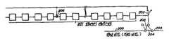
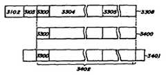
제17도는 본 발명에 따라 송신되는 패킷 신호를 도시한다. 표준 배열로 송신된 한 패킷 신호는 제17도에서 X로 표시된 8비트 단위로 분리되고 8비트 단위는 각가의 패킷으로 분리된다. 따라서 X로 표시되는 한 패킷 신호는 34패킷으로 분리되어 전송된다. 수신측에는 제17도에 도시된 것과 유사한 버퍼가 제공된다. 디코딩 경우에 있어서 X로 표시되는 8비트 단위는 버퍼에 연속적으로 로드되고 표준 배열 신호로 변환된다. 이때 각 패킷에 대해 에러 정정이 실행된다.Figure 17 shows a packet signal transmitted in accordance with the present invention. One packet signal transmitted in the standard arrangement is divided into 8-bit units indicated by X in FIG. 17, and 8-bit units are separated into respective packets. Thus, one packet signal, denoted by X, is divided into 34 packets and transmitted. The receiving side is provided with a buffer similar to that shown in FIG. In decoding cases, the 8-bit units, represented by X, are loaded into the buffer consecutively and converted into standard array signals. At this time, error correction is performed for each packet.
이와 같은 방법으로 각 패킷간에 8비트만큼 삽입된 배열을 사용함으로서 버스트의 형태로 패킷에 혼합된 잡음으로 인한 에러는 정정될 수 있다. 즉, 한 패킷 신호로 구성된 모든 비트는 에러이며(이러한 현상은 실제로 거의 일어나지 않으며 에러가 전체 패킷에 혼합된 경우조차도 평균치는 272/1=136비트이다), 이 에러는 각각 8비트로 분리될 수 있고 34패킷으로 일정하게 분리될 수 있다. 그 결과로 한 패킷(272비트)에러 임의로 발생되는 어떤 종류의 8비트 에러라도(272,190)에러 정정 모드로 정정될 수 있다.In this way, an error caused by noise mixed in the packet in the form of a burst can be corrected by using an array inserted by 8 bits between each packet. That is, all bits consisting of one packet signal are errors (this is rarely the case) and the average is 272/1 = 136 bits even when the error is mixed in the entire packet, and these errors can be separated into 8 bits each. It can be separated regularly into 34 packets. As a result, any kind of 8-bit error randomly generated in one packet (272 bits) (272, 190) can be corrected in the error correction mode.
즉 한 패킷의 데이타가 프레이밍 에러로 인해 손실되더라도, 신호의 도착이 검출되면 수신 신호가 정정될 확률이 1/2이므로 예정된 값 0이나 1을 구비하지 않는 것으로 가정함으로써 충분히 정정될 수 잇다. 수신된 신호가 상기와 같이 예정된 값을 구비하는 것으로 추정하면 평균 에러 비트의 수는 272/1=136비트이다. 마찬가지로 평균 두 프레이밍 에러가 있을 때 조차도 에러는 정정될 수 있다.In other words, even if data of one packet is lost due to a framing error, when the arrival of the signal is detected, the probability that the received signal is corrected is 1/2 so that it can be sufficiently corrected by assuming that it does not have a predetermined value of 0 or 1. Assuming that the received signal has a predetermined value as above, the average number of error bits is 272/1 = 136 bits. Similarly, even when there is an average two framing errors, the errors can be corrected.
패킷 신호가 상기와 같은 비트 배열로 전송될 때 버스트의 형태로 발생되는 자동차의 잡음과 같은 도시형 잡음과 가정용 전기장로부터의 임펄스 잡음이 충분히 제거될 수 있다. 임의로 발생되는 잡음에 있어서 그 효율은 표준 배열의 경우에 있어서의 효율과 실제로 유사하다.When the packet signal is transmitted in such a bit array, urban noise such as automobile noise generated in the form of burst and impulse noise from a domestic electric field can be sufficiently eliminated. For randomly generated noise, the efficiency is actually similar to the efficiency in the case of the standard arrangement.
다음에는 수신측에서의 논리에 대해 기술하고자 한다. 수상기의 RAM은 제17도에 도시된 바와 같이 34×34=1156바이트 버퍼로 제공된다. A0를 선두 어드레스라고 하자. 이때 수신된 패킷 신호는 어드레스 A0내지 A0+33에 우선 기억된다. 그 다음에는 수신된 패킷이 어드레스 A0+34 내지 A0+67에 기억된다. 즉, n개의 어드레스를 갖춘 가장 새로운 패킷은 어드레스 A0+34(n-1) 내지 A0+34(n-1)+33에 기억된다. n이 34가 될 때 1156바이트 버퍼는 완전히 로드되고 패킷 신호의 에러 정정 작동이 시작된다. 에러 정정 회로에 로드되는 데이타가 제17도에서 X로 표시되며 어드레스는 A0,A0+35,A0+70,A0+150,…,A+1155로 표시된다. n이 35인 패킷 신호는 어드레스 A0내지 A0+33에 다시 기억된다. 따라서 제 n패킷 신호를 기억시키기 위한 어드레스를 표시하는 일반식은 다음과 같다.Next, the logic of the receiving side will be described. The receiver RAM is provided in a 34x34 = 1156 byte buffer as shown in FIG. Let A0 be the first address. The received packet signal is first stored at addresses A0 to A0 +33. The received packet is then stored at addresses A0 +34 to A0 +67. That is, the newest packet with n addresses is stored in addresses A0 +34 (n-1) to A0 +34 (n-1) +33. When n becomes 34, the 1156 byte buffer is fully loaded and the error correction operation of the packet signal begins. The data loaded into the error correction circuit is shown as X in FIG. 17 and the addresses are A0 , A0 +35, A0 +70, A0 +150,... , A + 1155. The packet signal with nequal to 35 is stored again at addresses A0 to A0 +33. Therefore, the general formula for indicating an address for storing the n-th packet signal is as follows.

여기서 { }는 잉여수이다. 제17도에서 디코딩된 패킷은 n이 35일 때 0으로 표시된다. 즉, A0+34, A0+68, A0+104,…, A0+33이다. 일반식은 다음과 같다.Where {} is a surplus number. The packet decoded in FIG. 17 is indicated by 0 when n is 35. FIG. That is, A0 +34, A0 +68, A0 +104,... , A0 +33. The general formula is:

마찬가지 방식으로 n이 36일 때 연속적으로 구해지며 n이 3일때도 연속적으로 구해진다. 이들 패킷 신호는 디코딩 코드에 로드되어 한 패킷내의 에러가 정정된다.In the same way, when n is 36, it is obtained continuously, and when n is 3. These packet signals are loaded into the decoding code so that errors in one packet are corrected.
제17도의 실시예에서 수신된 패킷 신호는 CPU의 RAM에 순차적으로 기록되며 패킷 신호가 에러 정정 디코더를 통과할 때 한 패킷이 디코딩된다. 이와 대조적으로 데이타가 패킷 버퍼에 로드될 때 데이타는 예정된 어드레스에 연속적으로 로드된다. 데이타가 판독될 때 34바이트는 연속 어드레스에서 판독되어 한 패킷에 해당하는 데이타가 직접 구해질 수 있게 된다. 제18도에 있어서 숫자는 전송된 패킷수를 나타낸다.In the embodiment of FIG. 17, the received packet signal is sequentially written to the RAM of the CPU and one packet is decoded when the packet signal passes through the error correction decoder. In contrast, when data is loaded into the packet buffer, the data is continuously loaded at the predetermined address. When data is read, 34 bytes are read from consecutive addresses so that the data corresponding to one packet can be obtained directly. In Fig. 18, the number indicates the number of packets transmitted.
일반식은 다음과 같이 나타낸다.General formula is represented as follows.

여기서 A0는 선두 에드레스를 나타내고 n은 n번째 패킷을 나타내며, { }는 잉여수를 나타낸다. 8비트 데이타가 본 발명에 따라 쓰여질 때 한 패킷에 대한 데이타는 34바이트 데이타를 연속 판독함으로써 구해질 수 있다. 이 경우에 선두 어드레스는 다음과 같이 주어진다.Where A0 represents the first address, n represents the nth packet, and {} represents a surplus number. When 8 bit data is written according to the present invention, the data for one packet can be obtained by continuously reading 34 byte data. In this case, the head address is given as follows.

제17도 및 제18도를 참고로 하여 기술된 상기 방법은 1바이트 데이타가 1패킷을 지연시킴으로써 연속적으로 전송되게 하는 것이다. 한 패킷에 대한 데이타는 34패킷을 수신한 후 기억된다. 원리적으로는 각 바이트(8비트)를 임의로 배열하여 이러한 도청 방지용 비밀 전송이 비밀 전송으로서 유료 텔레비젼 시스템에 사용될 수 있게 된다.The method described with reference to Figs. 17 and 18 allows one-byte data to be transmitted continuously by delaying one packet. Data for one packet is stored after receiving 34 packets. In principle, each byte (8 bits) can be arbitrarily arranged so that this eavesdropping secret transmission can be used in pay television systems as a secret transmission.
제19도에 있어서, 다수의 패킷 가운데 각 바이트는 도청 방지를 위해 비밀 전송하는 기본 원리를 설명하기 위해 제17도에 도시된 제2 및 제3바이트만이 서로 바꾸어진다. 수상기는 제19도에 도시된 패킷 버퍼를 구비하며, 34번째 패킷이 수신될 때 X로 표시된 바이트가 판독된다. 따라서, 1패킷에 대한 데이타가 재구성 되어 디코드된다. 마찬가지 방법으로 35번째 패킷을 수신하자마자 0으로 표시된 바이트가 판독되고 36번째 패킷을 수신하자마자 △로 표시된 바이트가 판독되며 37번째 패킷을 수신하자마자 ●로 표시된 바이트가 판독된다. 물론 35번째 패킷은 어드레스 A0로부터 기억되고 36번째 패킷은, 어드레스 A0+34에서 시작되는 어드레스에 수신되며 37번째 패킷은 어드레스 A0+68부터 기억된다. A0는 패킷 버퍼의 선두 어드레스를 나타낸다. 각 패킷의 선두 바이트가 전송 순서에 따라 연속적으로 송신되면 유효 패턴의 수는 다음과 같이 주어진다.In FIG. 19, only the second and third bytes shown in FIG. 17 are interchanged with each other to explain the basic principle of secret transmission for the prevention of eavesdropping among the plurality of packets. The receiver has the packet buffer shown in FIG. 19, and the byte indicated by X is read when the 34th packet is received. Thus, data for one packet is reconstructed and decoded. In the same way, the byte indicated by 0 is read as soon as the 35th packet is received, the byte indicated by Δ is read as soon as the 36th packet is received, and the byte indicated by ● as soon as the 37th packet is received. Of course, the 35 th packet is stored from address A0 , the 36 th packet is received at an address starting at address A0 +34, and the 37 th packet is stored from address A0 +68. A0 represents the head address of the packet buffer. If the first byte of each packet is transmitted consecutively in the transmission order, the number of valid patterns is given as follows.

텔레비젼 신호의 수직 귀선 소거 주기에 1H를 이용함으로써 하루에 전송될 수 있는 패킷의 총수는 다음과 같다.The total number of packets that can be transmitted in one day by using 1H in the vertical blanking period of the television signal is as follows.

따라서 본 발명에 따른 도청 방지용 비밀 전송에 관한 기본원리를 알고 있다 할지라도 비밀 전송 패턴을 모르면 수신측에서 임의의 패턴을 만들어 송신 패턴이 조사될 때 조차도 암호 해독을 위해 10 일이 필요하다. 따라서 해독이 불가능하게 된다.Therefore, even if the basic principle of the eavesdropping secret transmission in accordance with the present invention is known, if the secret transmission pattern is not known, it takes 10 days for decryption even when the transmission pattern is examined by making a random pattern at the receiving side. Therefore, it becomes impossible to decipher.
더 나아가 34바이트를 각각 반전시키는 정보가 데이타가 부가되면 2 패턴이 유효하여 천문학적 숫자인 233×1029일이 필요하게 된다.Furthermore, if data is added that inverts 34 bytes each, two patterns are valid, requiring 233 x 1029 days, which are astronomical numbers.
제20도는 상기 비밀 전송을 해독하기 위한 ROM정보를 도시한다. ROM의 비트수는 다음과 같다.20 shows ROM information for decrypting the secret transmission. The number of bits of the ROM is as follows.

제20도에서 어드레스는 첫째 패킷을 재기억시키는데 필요한 바이트수와 일치하는 패킷수를 나타낸다. 이 어드레스는 0에서 33까지 나타내기에 충분하여 5비트가 충분하다. 반전 정보는 한 패킷의 각 바이트가 반전되어 전송되었는지 아니지를 보여준다. 이러한 목적을 위해 1비트만이 필요하다.In FIG. 20, the address represents the number of packets that matches the number of bytes needed to re-memorize the first packet. This address is sufficient to represent 0 to 33, so 5 bits are sufficient. The inversion information shows whether each byte of a packet has been inverted and transmitted. Only 1 bit is needed for this purpose.
방송국이 제20도에 도시된 바와같은 새로운 ROM만을 부여하면 방송국이 도청 방지용 비밀 어드레스 및 반전 정보를 변경시킬 때마다 허가없이 혹은 ROM 없이는 그 방송국이 프로그램을 시청할 수 없다.If a broadcaster only assigns a new ROM as shown in Fig. 20, the broadcaster cannot watch the program without permission or without the ROM every time the broadcaster changes the eavesdropping secret address and reverse information.
상기 어떠한 비밀 시스템이 사용된다 하더라도 시스템은 기능을 충분히 발휘한다. 반전 정보 및 비밀 어드레스는 16,34,68과 같은 다수의 비트마다 대해 지정된다.No matter what secret system is used, the system is fully functional. Inversion information and secret addresses are specified for multiple bits, such as 16,34,68.
상기된 바와 같이 문자 방송을 위해 한 패킷을 형성하는 각각의 바이트가 다른 패킷에 의해 전송되는 실시예에서는 비트 에러가 버스트 형태로 발생될 때 조차도 에러 정정 능력을 향상된다. 본 발명에 따라(272,190)코드를 사용하는 8비트 에러 정정 방법에 따르면 한 패킷 정보가 손실되더라도 모든 정보가 재기억될 수 있다. 즉 프레이밍 에러가 발생할 때 조차도 다른 33개의 패킷에 에러가 없으면 모든 에러가 정정될 수 있다.As described above, in the embodiment in which each byte forming one packet for text broadcasting is transmitted by another packet, the error correction capability is improved even when a bit error occurs in burst form. According to the 8-bit error correction method using the code (272,190) according to the present invention, even if one packet information is lost, all the information can be re-memorized. That is, even when a framing error occurs, all errors can be corrected if there are no errors in the other 33 packets.
제17도에 도시된 실시예의 경우에 있어서 수상기는 34×34바이트의 패킷 버퍼를 구비하며 수신 패킷 신호는 패킷 버퍼에 순환 기록되어 각각의 바이트는 경사지게 판독될 수 있게 된다. 따라서 한 패킷에 대한 신호는 재구성될 수 있다.In the case of the embodiment shown in FIG. 17, the receiver has a packet buffer of 34x34 bytes and the received packet signal is cyclically written to the packet buffer so that each byte can be read out obliquely. Thus, the signal for one packet can be reconstructed.
제18도에 도시된 실시예에 수신 패킷 신호는 예정된 규칙에 따라 경사지게 기록되어 34바이트를 연속적으로 판독함으로써 한 패킷 신호가 구해질 수 있게된다.In the embodiment shown in Fig. 18, the received packet signal is written obliquely according to a predetermined rule so that one packet signal can be obtained by continuously reading 34 bytes.
제19도에 도시된 실시예의 경우에 있어서 신호가 전송될때 전송될 각 바이트의 패킷은 임의로 배열되어 이 실시예가 주파수 대 변환기에 적용될 수 있게 되는 반면에 에러 정정 능력은 상기 실시예의 경우와 동일하게 유지될 수 있다. 다라서 방송국은 이러한 실시예를 유료 텔레비젼 시스템에서 장려한다.In the case of the embodiment shown in Fig. 19, when a signal is transmitted, the packet of each byte to be transmitted is arbitrarily arranged so that this embodiment can be applied to the frequency-to-converter while the error correction capability remains the same as that of the above embodiment. Can be. The broadcaster therefore promotes this embodiment in pay television systems.
제19도에 도시된 실시예 뿐만 아니라 제20도에 도시된 실시예의 경우에 있어서도 각 바이트에 대한 반전 정보는 데이타에 부가되어 텔레비젼 도청이 극히 어렵게 된다.In the case of the embodiment shown in FIG. 19 as well as the embodiment shown in FIG. 19, the inversion information for each byte is added to the data, making television eavesdropping extremely difficult.
상기 제1도 내지 제20도를 참고로 하여 기술된 본 발명은 에러 정정이 실행될 수 없을 경우 에러를 정정하기 위해 비트 위치를 이동시킬 수 있는 장점이 있다. 마찬가지로, 근본적으로 정정될 수 없는 8비트 이상의 에러가 정정되는 가능성을 증가시킬 수도 있다. 또한, 에러 정정 능력은 저하되지 않는다. 따라서 본 발명은 문자 방송 시스템에서 에러를 정정할 때 매우 효과적이며 따라서 문자 방송 지역은 상당히 확대될 수 있게 된다.The present invention described with reference to FIGS. 1 through 20 has an advantage that the bit position can be shifted to correct an error when the error correction cannot be performed. Likewise, it may increase the likelihood that an error of 8 bits or more that cannot be fundamentally corrected is corrected. In addition, the error correction capability is not degraded. Therefore, the present invention is very effective in correcting errors in a text broadcasting system, and thus the text broadcasting area can be significantly expanded.
상기 실시예에서 정보가 코딩되는 디지털 신호가 텔레비젼 신호의 귀선 소거 주기에 삽입되는 것으로 기술된 반면에, 이러한 디지털 신호는 전송 선로에 여러 가지 형태로 삽입될 수 있거나 이러한 디지털 신호는 단독으로 사용될 수도 있다.While the digital signal in which the information is coded is described as being inserted in the blanking period of the television signal in the above embodiment, this digital signal may be inserted in various forms in the transmission line or such a digital signal may be used alone. .
상기된 바와 같이(272,190)코드를 이용하는 에러 정정 방법은 일본이나 그외 다른 나라에서처럼 문자 방송 시스템용으로 가장 적합하다. 그러나 상기 기본적인 에러 정정 방법이 사용될 때 272비트로 구성된 한 패킷내의 8비트 에러는 정정할 수 있지만 8비트 이상의 에러는 거의 정정할 수 없다. 에러가 정정될 수 없을 경우 선두 비트가 이동되어 8비트 이상의 에러가 정정될 수 있게 되는 상기 개선된 에러 정정 방법에 따르면 처리 시간이 길어지는 단점이 있다As described above, the error correction method using the (272, 190) code is most suitable for a text broadcasting system as in Japan or other countries. However, when the basic error correction method is used, an 8-bit error in a packet consisting of 272 bits can be corrected, but an error more than 8 bits can hardly be corrected. According to the improved error correction method in which the leading bit is shifted when the error cannot be corrected so that an error of 8 bits or more can be corrected, the processing time is long.
따라서 제21도 내지 제25도에는 에러 정정 능력을 개선할 뿐만 아니라 처리 시간을 단축시키기도 하는 에러 정정 방법이 기술된다.Therefore, FIGS. 21 to 25 describe error correction methods that not only improve the error correction capability but also shorten the processing time.
제21도에는 본 발명에 따른 에러 정정 회로에 대한 실시예가 도시된다. 제21도에는 출력 포트(1100), 입력 포트(1101), 병렬-직렬 및 직렬-병렬 변환기(1102), 272단계를 갖춘 데이타 레지스터(1103), 타이밍 발생기(1104), 로드 게이트 회로(1105), 82단계를 갖춘 신드롬 레지스터(1106), 다수결 논리 회로(1107), 정정 게이트 회로(1108), 에러 상태 레지스터(1109), 시작 레지스터(1110), 로드 신호(1111), 정정 신호(1113), 정정될 데이타(1114), 정정된 데이타(1115), 연속 로드 데이타(1116),준비 신호(1117), 신드롬 레지스터 신호(1118), 에러 정정 신호(1119), 로드 게이트 신호(1120), 정정 게이트 신호 (1121), 로드 타이밍 신호(1122), 로드 클럭 신호 (1123), 클리어 신호(1124), 에러 정정 클럭 신호(1126), 에러 상태 신호(1127), 모듈 2가산기(1128) 및 임계치 지정 신호(5비트)(1129)가 있다.21 shows an embodiment of an error correction circuit according to the present invention. 21 shows an
본 실시에의 기본적인 회로 구성은 첫째, 임계치는 신호(129)에 응답하여 변할 수 있게 구성한 점, 둘째, 직교 패리티 검사합 소자는 1비트 단축된 후 선두 비트를 구비하는 점을 제외하면, 제1도 내지 제20도를 참고로 하여 기술된 실시예의 구성과 실제로 유사하다. 따라서 전송 데이타의 선두 비트가 직교하면 로드 종료 신호가 제거된다.In the basic circuit configuration of the present embodiment, first, the threshold is configured to be changed in response to the signal 129, and second, the orthogonal parity check-sum element is shortened by one bit and then has the first bit. It is actually similar to the configuration of the embodiment described with reference to Figs. Therefore, when the first bit of the transmission data is orthogonal, the load end signal is removed.
다음에는 작동에 대해 기술된다. 이 실시예는 임계치를 17,16,15,14,13,12,11,10,9의 순으로 감소시킴으로써 정정이 실시되어 에러 정정 능력은 아래 기술되는 바와 같이 개선되는 특성이 있다.The following describes the operation. This embodiment has the characteristic that the correction is performed by decreasing the threshold in the order of 17, 16, 15, 14, 13, 12, 11, 10, 9 so that the error correction capability is improved as described below.
첫째, CPU(도시 안됨)는 임계 레벨을 17(5비트 정보)로 세트시킨다. 그후 CPU는 시작 명령(시작 신호1110)을 발생시켜 신드롬 레지스터(1106)의 전체 82비트는 0으로 세트된다(리세트 신호(1124) 참조).First, the CPU (not shown) sets the threshold level to 17 (5-bit information). The CPU then issues a start command (start signal 1110) so that all 82 bits of the
그 결과로 다음 데이타가 로드될 준비가 된다. CPU는 1패킷에 해당하는 272비트로 구성된 정보가 16비트 집단으로 분리시켜 연속적으로 17회 로드시킨다. CPU는 로드 데이타를 정정될 데이타(1114)상에 로드시켜 로드 명령이 발생되게 한다(로드 신호(1111) 참조).As a result, the next data is ready to be loaded. The CPU loads 17 consecutive bits of 272 bits of information into one 16-bit group. The CPU loads the load data onto the data 1114 to be corrected so that a load command is generated (see load signal 1111).
로드 신호(1111)에 응답하여 로드 게이트 신호(1120) 및 로드 클럭 신호(16비트(1123))가 발생된다. 그 결과로 신드롬 레지스터(1106)의 데이타를 앞서기 위하여 로드 게이트 회로(1105)가 제어되고 정정될 데이타(1114)가 병렬-직렬 변환기(1102)에 로드되며 병렬-직렬 변환기(1102)에서 데이타 레지스터(1103)에 전송되는 데이타가 16비트만큼 이동되며 신드롬 레지스터(1106)내의 데이타가 16비트만큼 이동된다.The
상기 작동은 17회 반복되어 선두 데이타는 데이타 레지스터(1103)의 선두에 이르게 된다. 신드롬 레지스터(1106)는 이미 신드롬을 발생시켰다. 즉, 82비트 신드롬 레지스터(1106)는 발진기 다항식 G(2)에 의해 데이타를 분리시킴으로써 구해지는 잉여 집단을 나타낸다.The above operation is repeated 17 times so that the head data reaches the head of the

여기서 S(x)는 신드롬이고, a0…a271은 727비트로 구성된 데이타이며, g(x)는 제1도 내지 제20도를 참조하기 전에 설명되는 생성 다항식이며, { }는 잉여집단을 표시한다.Where S (x) is a syndrome and a0 ... a271 is 727 bits of data, g (x) is a generation polynomial described before referring to FIGS. 1 to 20, and {} indicates a surplus population.
다음에는 에러 정정 작동에 관하여 설명한다. 정정 명령에 응답하여 CPU는 정정 신호(1113)를 발생시킨다. 한편, 타이밍 발생기(1104)는 에러 정정 클럭 신호(1126)를 발생시켜 데이타 레지스터(1103)내에 기억된 데이타중 16비트만이 정정된 후 직렬-병렬 변환기(102)에 로드된다. 이러한 에러 정정은 EOR회로(즉, 모듈로 2가산기)(1108)에 의해 수행된다. 에러 정정 신호(1119)는 신드롬 레지스터의 82비트 내용에서 17개의 선형 조합을 만든다. 17개의 조합은 다수결 논리 회로(1107)(임계치 지정 신호(1129)에서 초기 임계치는 17이다)에서 비교되어 출력이 유도된다.The following describes the error correction operation. In response to the correction command, the CPU generates a
그러나 에러 정정 신호(1119)는 이 정정 신호가 정정 게이트 신호(1121)에 응답하여 에러가 정정될 경우에만 정정되도록 구성된다(정정 게이트 신호(1108) 참조). 에러 정정의 경우에 있어서와 같이 1비트 에러가 있으면 에러 정정 신호(1119)는 신드롬 레지스터(1106)의 내용을 수정하여 이 비트의 영향은 제거되게 된다.However, the error correction signal 1119 is configured such that this correction signal is corrected only when the error is corrected in response to the correction gate signal 1121 (see correction gate signal 1108). As in the case of error correction, if there is a 1-bit error, the error correction signal 1119 modifies the contents of the
16비트 에러가 정정 신호(1113)에 응답하여 이러한 방식으로 정정된후 CPU는 준비 신호(1117)가 발생되었는지 아닌지를 확인한 다음 입력 포트(1101)에서 데이타(1115)를 판독한다. 정정 신호(1113)은 17회 출력되어 272비트로된 1패킷으로 구성된 신호가 재기억된다. 이 경우 정확하게 정정되었는가 아닌가는 에러 상태 신호(1127)를 조사함으로써 검출될 수 있다. 신드롬 레지스터(1106)의 내용이 모두 0이 아니면 아직도 에러 비트가 실재하게 되어 에러 정정이 다시 실행된다. 이 경우에 있어서 다수결 논리 회로(1107)의 임계치는 1만큼 감소된다. 즉, 새로운 임계치는 16이 되고 임계치 17를 정정한 데이타가 사용된다.After the 16-bit error is corrected in this manner in response to the
상기 작동은 임계치가 9가 될 때까지 반복된다. 그러나 신드롬 레지스터(1106)의 내용이 작동 진행 과정동안 모두 1이 될 때 에러 정정 작동이 완료된 것으로 간주된다. 다시 말하면 이 시간점에서 데이타는 정확한 값을 구비하여 이 시간 이후에 데이타를 에러 정점 회로에 인가시킬 필요가 없게 된다. 이 실시예에서는 입력 포트 및 출력 포트상의 데이타가 16비트를 구비하는 동안 어떠한 필요 비트수도 유사한 방식으로 받아들일 수 있다.The operation is repeated until the threshold is nine. However, the error correction operation is considered complete when the contents of the
제22도는 제21도에 도시된 바와 같은 회로의 제어 절차를 보여주는 풀로우챠트를 도시한다. 이 경우 회로 배치를 단순화시키기 위해 직교 패리티 검사 회로가 사용된다. 즉, 직교 패리티 비트합은 단축 비트상에서 직교하는 것이 아니라 실제 전송 비트의 선두에서 직교한다. 따라서 상기된 바와 같이 신드롬 레지스터의 휴지 작동은 로드 종료 명령 신호에 응답하여 제거될 수 있다. 다시 말하면, 로드 종료 신호는 필요하지 않다.FIG. 22 shows a pull chart showing the control procedure of the circuit as shown in FIG. In this case, orthogonal parity check circuits are used to simplify circuit arrangement. That is, the orthogonal parity bit sum is not orthogonal on the short bits but orthogonal at the head of the actual transmission bit. Thus, as described above, the idle operation of the syndrome register can be removed in response to the load end command signal. In other words, no load termination signal is required.
S0,S1,…,S8z,S81,을 신드롬 레지스터(1106)의 내용이라고 하자, 이때 전송 비트의 선두에서 직교하는 직교 패리티 검사합 A0,A1…,A16다음과 같이 주어진다.S0 , S1 ,... Let, S8z , S81 , be the contents of the

다음에는 다수결 논리 회로의 임계치(가령, 17,16,15,…,9)를 변별함으로써 얻어지는 장점에 관하여 설명한다. 예를들어, 임계치가 17이라고 가정하자. 이때 에러의 수가 16 이하일 때 오정정은 일어나지 않을 것이다. 그러나 임계치가 9일 때 오정정이 발생할 수 있다. 감축된 비트가 제거되면 직교 패리티 검사합으로 구성되는 행렬 A는 다음과 같이 구해진다.Next, the advantages obtained by discriminating the thresholds (e.g., 17, 16, 15, ..., 9) of the majority vote logic circuit will be described. For example, suppose the threshold is 17. If the number of errors is less than 16, no miscorrection will occur. However, a miscorrection can occur when the threshold is nine. When the reduced bits are removed, the matrix A consisting of orthogonal parity check sums is obtained as follows.

선두 비트의 위치를 제외한 에러가 16개 이하이면 에러 패턴과 행렬 A의 곱에서 1이 수는 최대로 해도 16개이다. 임계치는 17이므로 에러 정정이 실행되지 않게 된다. 즉, 오정정이 일어나지 않는다. 16비트 이하의 에러가 선두 비트도 포함한다면 에러 패턴과 행렬 A의 곱은 17이 된다. 따라서 선두 비트가 에러이라면 에러수는 17이 된다. 15개의 에러가 선두 비트를 포함하는 행렬 A의 각 열에 구성되면 1의 수는 17개가 된다. 이 경우에 선두 비트는 정정되어 선두 비트만이 정확히 정정되게 된다. 상기 작동은 272회 반복된다. 따라서 임계치가 17이면 일부 에러가 정정되고 16개 이하의 에러가 있을 경우에는 오정정이 일어나지 않는다.If there are 16 or less errors except the position of the first bit, the number of 1's in the product of the error pattern and the matrix A is 16 even if the maximum is. Since the threshold is 17, no error correction is performed. In other words, no correction occurs. If an error of 16 bits or less also includes the first bit, the product of the error pattern and the matrix A is 17. Therefore, if the first bit is an error, the number of errors is 17. If 15 errors are formed in each column of the matrix A including the first bit, the number of 1s is 17. In this case, the leading bit is corrected so that only the leading bit is corrected correctly. The operation is repeated 272 times. Therefore, if the threshold is 17, some errors are corrected, and if there are 16 or less errors, no miscorrection occurs.
그 다음에는 임계치가 1/16로 감소되고 상기 작동과 동일한 작동이 반복된다. 15개 이하의 에러가 있으면 오정정이 실행되고 얼마간의 에러는 정정된다.Then the threshold is reduced to 1/16 and the same operation as the above operation is repeated. If there are less than 15 errors, miscorrection is performed and some errors are corrected.
임계치는 15,14,13,12,11,10과 같은 방식으로 감소되고 에러 정정이 실행된다. 그 결과로 실제 에러수(16비트나 9비트)가 정정된다.The threshold is reduced in the same manner as 15, 14, 13, 12, 11, 10 and error correction is performed. As a result, the actual number of errors (16 bits or 9 bits) is corrected.
끝으로, 임계치는 원래의 값인 9로 세트되고 에러 정정이 이루어진다. 이 경우에 코드의 에러 정정 능력 때문에 8비트 이하의 잔여 에러가 정정될 수 있다.Finally, the threshold is set to its original value of 9 and error correction is made. In this case, residual errors of 8 bits or less may be corrected because of the error correction capability of the code.
상기된 바와 같이 본 발명에 따르면 임계치는 17에서 9로 연속적으로 감소되어 8비트 이하의 에러와 9내지 16비트 에러의 대부분은 정정될 수 있다.As described above, according to the present invention, the threshold is continuously reduced from 17 to 9 so that the error of 8 bits or less and most of 9 to 16 bit errors can be corrected.
제23도는 본 발명에 따른 또 다른 실시예를 도시하며 제24도는 CPU(도시 안됨)의 제어 절차를 설명하기 위한 플로우챠트를 도시하고 있다.FIG. 23 shows another embodiment according to the present invention, and FIG. 24 shows a flowchart for explaining a control procedure of a CPU (not shown).
제21도에 도시된 바와 같은 에러 정정 회로에서 임계치는 필요에 따라 세트되며 에러 정정에 의해 구해지는 데이타는 재정정을 위해 다시 로드된다. 그 결과로 상당히 오랜 처리 시간이 필요하다. 제23도에 도시된 바와 같은 에러 정정 회로에서 거의 모든 회로 성분이 하드웨어이므로 처리 시간이 빨라진다. 제23도에 도시된 회로는 에러 정정 처리 및 임계치 설정이 제23도에 도시된 바와 같은 실시예에서 자동적으로 실행된다는 점을 제외하면 제21도에 도시된 회로와 실제로 유사한 구조를 구비하여 동일한 참조번호는 제21도 및 제23도 모두 동일 부분을 지정하는데 사용된다.In the error correction circuit as shown in FIG. 21, the threshold is set as needed and the data obtained by the error correction is reloaded for redefinition. As a result, considerably longer processing times are required. In the error correction circuit as shown in FIG. 23, since almost all the circuit components are hardware, the processing time is faster. The circuit shown in FIG. 23 has substantially the same structure as the circuit shown in FIG. 21, except that the error correction processing and threshold setting are automatically executed in the embodiment as shown in FIG. The numbers 21 and 23 are used to designate the same parts.
제23도에는 데이타 선택기(1300), 타이밍 발생기(1301), 다수결 논리 회로(1302), 데이타 판독 신호(1303), 의사 클럭 신호(1304), 데이타 로드 클럭 신호(1305), 정정 클럭 신호(1306), 다음에 이용하기 위해 보존된 데이타(1307), 에러가 정정된 연속 신호(1308), 한 패킷의 데이타 검사가 완료된 시간 지점에서 발생되는 타이밍 신호(1309)가 예시된다.23 shows a
제21도를 참고로 하여 기술된 바와 같이 CPU는 시작 신호(1110)를 발생시킨다. 이 시작 신호에 응답하여 타이밍 발생기(1301)는 리세트 신호(1124)를 발생시켜 신드롬 레지스터(1106)의 내용이 모두 클리어되게 된다. 동시에 다수결 논리 회로(1302)의 임계치는 17로 설정된다. 그 다음에 CPU는 정정될 데이타를 병렬 데이타로서 세트시키고 로드 신호(1111)를 발생시켜 데이타가 로드된다. 로드 클럭 신호(1112)에 응답하여 데이타가 병렬-직렬 변환기(1102)에 로드된다. 병렬 로드의 로드 클럭 신호(1123)에 응답하여 데이타는 데이타 레지스터(1103) 및 신드롬 레지스터(1106)에 로드된다. 데이타 선택기(1300)는 데이타가 로드될 때 로드된 데이타를 통과시키고 에러가 정정될 경우 데이타(1307)가 보존되도록 통과시키기 위한 게이트회로이다. 따라서, 전체 272비트를 한 패킷에 로드시키는 것이 완료된다.As described with reference to FIG. 21, the CPU generates a
데이타의 로드 종료후 타이밍 발생기(1301)는 에러 정정 신호를 발생시킨다. 즉, 정정 게이트(108)는 개방되고, 정정 클럭 신호(1306)에 응답하여 신드롬 레지스터(1106)가 이동되며, 데이타 레지스터(1103)도 에러 정정을 위해 이동된다. 처음 사용된 임계치는 17이다. 제21도의 경우에 있어서와 같이 전체 272비트는 에러 정정된다. 이 경우에 임계치인 17로 정정된 데이타(272비트)는 데이타 레지스터(1103)에 남겨진다.After the end of loading of data, the timing generator 1301 generates an error correction signal. That is, the correction gate 108 is opened, the
이 단계에서 에러 상태 신호(1127)가 에러를 도시하면 데이타 레지스터(1103)에 기억된 데이타는 아직까지 에러이다. 따라서 임계치는 1만큼 감소되고 에러 정정이 반복된다.If the
다수결 논리 회로(1302)는 에러 상태 신호(1127)를 수신한다. 다수결 논리 회로가 에러가 있다는 것을 검출할 때 임계치는 한 패킷 종료 신호의 타이밍에 응답하여 1만큼 감소된다. 신드롬 레지스터(1106)의 주기는 273비트이어서 신드롬 레지스터(1106)의 내용은 의사 클럭 신호(1304)에 응답하여서 1비트만큼 이동된다.The majority
그 다음에 에러 정정은 임계치인 16을 이용하여 계속된다.Error correction then continues using the threshold of 16.
에러 상태 신호(1127)가 모든 에러가 정정되었다는 것을 나타낼 때 CPU는 데이타의 판독 주기에 들어간다.The CPU enters a read cycle of data when the
모든 에러가 정정되지 않았다면 임계치가 9로 감소될 때 조차도 에러 상태 신호(1127)는 에러를 나타내며 준비 신호(1117)가 발생된다.If all errors have not been corrected, even when the threshold is reduced to 9, the
데이타 판독 신호(1303)에 응답하여 데이타가 판독된다. 데이타 레지스터(1103)의 데이타는 데이타 판독 클럭 신호(1305)에 응답하여 직렬-병렬 변환기(1102)에 전달된다. CPU는 준비 신호(1117)에 응답하여 판독용 데이타 판독 신호(1303)를 병렬 데이타(1115)에 출력시켜 에러가 정정된 후 1패킷의 데이타가 복원된다.Data is read in response to the data read
제25도는 다수결 논리 회로의 작동을 설명하는데 사용되는 블록선도이다. 제25도에는 다수결 논리 회로에 속하는 다수결 논리 소자(A0내지 A16)의 입력 신호(1500), 감산기(1501),(1502), 게이트 신호(1503), 임계치를 1만큼 감소시키는 감산 명령 신호(1504), 임계치 신호(1505) 및 다수결 논리 회로(1501)의 출력(1506)이 있다. 상기된 바와 같이 제25도에는 정정 게이트 신호(1108), 리세트 신호(1124), 에러 상태 신호(1127) 및 패킷 종료 신호(1309)도 있다.25 is a block diagram used to explain the operation of a majority vote logic circuit. 25 shows a subtraction command signal for reducing the
감산기(1502)는 리세트 신호(1124)에 응답하여 17로 세트된다. 즉, 제1임계치는 17이다. 272비트가 한번에 1비트씩 정정될 때 게이트(1503)는 1패킷 종료 신호(1309)에 응답하여 인에이블되어 에러 상태 신호(1127)가 이 게이트를 통과하게된다. 초기 임계치인 17은 감상 명령 신호(1504)에 응답하여 1이 감소되어 16이되고 임계치 신호(1505)가 전송된다. 다수결 논리 회로(1501)는 입력 신호 A0내지 A16가 임계치 신호(1505)에 의해 표시되는 예정된 임계치 이상일때만 출력 신호(1506)을 유도한다. 상기의 작동은 각 비트에 대해 실행되어 이에 의해 임계치 16에 의한 작동이 완료된다.The
임계치 15 내지 9에 대해서도 마찬가지의 작동이 반복된다.The same operation is repeated for the thresholds 15-9.
제21도 및 제23도에 도시된 바와 같은 실시예에서 임계치는 에러 정정을 위해서 17에서 9까지 순차적으로 감소된다. 그러나 중간 임계치 11,10,9가 선택되면 처리 시간은 단축될 것이다. 즉, 9비트 이하의 총 에러와 대부분의 9비트 및 10비트 에러는 정정된다. 더 나아가 임계치가 17,15,13,11,19와 같이 감소되면 에러 정정 시간도 단축될 수 있다.In the embodiment as shown in FIGS. 21 and 23, the threshold is sequentially reduced from 17 to 9 for error correction. However, if the
상기된 바와 같이 9비트 이하의 전체 에러는 완전히 정정될 수 있으며 16비트 내지 9비트의 대부분의 에러도 정정될 수 있다. 따라서 문자 방송 지역은 증가될 수 있고 에러 표시는 최소화될 수 있다. 컴퓨터 시뮬레이션에 따르면 9비트 및 10비트의 경우 에러는 100% 완전 정정되며 11비트의 경우 에러는 95%까지 정정된다.As described above, the overall error of 9 bits or less can be completely corrected, and most errors of 16 to 9 bits can also be corrected. Therefore, the text broadcasting area can be increased and the error indication can be minimized. Computer simulations show that the error is 100% fully corrected for 9 and 10 bits, and the error is corrected to 95% for 11 bits.
제21도 도시된 바와 같은 실시예에서 기본 에러 정정 회로를 수정하지 않고서 임계치만이 외부에서 지정되어 몇가지 하드웨어를 종래의 회로에 부가시킴으로써 본 발명이 간단하게 실행되는 장점이 있다.In the embodiment as shown in Fig. 21, only the threshold is externally specified without modifying the basic error correction circuit, so that the present invention is simply implemented by adding some hardware to the conventional circuit.
제23도에 도시된 바와 같은 실시예의 경우에 있어서 제21도에 도시된 바와 같은 실시예에 사용되는 소프트웨어는 하드웨어로 대체되어 고속 작동이 가능하게 된다.In the case of the embodiment as shown in FIG. 23, the software used in the embodiment as shown in FIG. 21 is replaced with hardware to enable high speed operation.
최종 실시예에서 점차로 감소되는 임계치의 수는 감소되어 에러 정정에 필요한 시간은 단축될 수 있다.In the last embodiment the number of thresholds that are gradually reduced can be reduced so that the time required for error correction can be shortened.
제21도 내지 제25도를 참고로 하여 상기된 실시예는 텔레비젼 신호의 수직 귀선 소거 주기를 이용하는 문자 방송 시스템에 적용될 수 있지만 본 발명은 모든 수평 라인이 사용되는 배타형 코드 방송 시스템에 동일하게 적용될 수 있다.21 to 25 may be applied to a character broadcasting system using a vertical blanking period of a television signal, but the present invention is equally applicable to an exclusive code broadcasting system using all horizontal lines. Can be.
제1도 내지 제25도를 참고로 하여 기술된 상기 실시예에서는 정정될 수 없는 다소의 에러가 실재하는 공통적인 단점이 있다. 따라서 제26도 내지 제29도에는 에러의 정정 가능성이 감소될 수 있는 에러 검출회로에 대해 기술된다.In the above-described embodiment described with reference to Figs. 1 to 25, there is a common disadvantage in that there are some errors that cannot be corrected. Thus, FIGS. 26 to 29 describe an error detection circuit in which the possibility of error correction can be reduced.
제26도는 본 발명에 따른 에러 검출 회로의 한 실시예를 도시한다. 제27도는 임계치가 감소되는 동안 에러 정정이 실행될 때 시뮬레이션의 경과를 도시하며 즉, 제27도는 임계치로 인한 정정 능력간의 차를 도시한다.Figure 26 shows one embodiment of an error detection circuit according to the present invention. FIG. 27 shows the progress of the simulation when error correction is executed while the threshold is reduced, i.e., FIG. 27 shows the difference between the correction capabilities due to the threshold.
제27도에서 1은 다수결 논리 회로의 초기 임계치를 나타낸다.In FIG. 27, 1 represents the initial threshold of the majority vote logic circuit.
제28도는 제26도에 도시된 바와 같은 실시예를 제어하기 위한 플로우챠트를 도시한다. 제28도에서 *로 표시된 블록은 CPU에 의해 실행된다. 나머지 단계는 제26도의 회로에 의해 자동적으로 실행된다. 제28도에 도시된 바와 같은 단계는 제26도에 도시된 실시예의 설명과 연관하여 설명된다.FIG. 28 shows a flowchart for controlling the embodiment as shown in FIG. Blocks marked with * in FIG. 28 are executed by the CPU. The remaining steps are executed automatically by the circuit of FIG. Steps as shown in FIG. 28 are described in connection with the description of the embodiment shown in FIG.
제26도에는 CPU 출력 포트(CPU는 도시되지 않음)(2100), 병렬-직렬 변환기(2101), 선택기(2102), 데이타 레지스터(272비트)(2103),모듈로 2가산기(2104), CPU 입력 포트(2105), 게이트(2106), 모듈로 2가산기(2107), 타이밍 발생기(2108), 신드롬 레지스터(28비트)(2109), 다수결 논리 회로(2110), 에러 정정 신호(2111), 클럭 신호(2112), 정정될 데이타(2113), 정정된 데이타(2114), 리세트 신호(2115),로드 신호(2116), 페치 신호(2117), 에러 상태 신호(2118), 준비 신호(2119), 데이타 로드 제어 신호(2120), 데이타 로드 펄스 신호(2121), 데이타 로드 클럭 신호(2122), 에러 정정 게이트 신호(2123), 에러 정정 신호(2124), 신드롬 시프트 클럭 신호(2125), 페치 클럭 신호(2126), 연속 로드 데이타(2127), 순환 데이타(2128), 신드롬 레지스터 신호(2929), 임계치 저감 신호(2130) 및 에러 정정 불가 신호(2131)가 있다.26 shows a CPU output port (CPU not shown) 2100, a parallel-to-
CPU는 패킷 신호를 수신하고 에러 정정 처리를 시작한다. 우선 CPU는 리세트 신호(2115)를 발생시킨다. 그래서 신드롬 레지스터(2109)의 82비트는 모두 0으로 세트되고 타이밍 발생기(2108)는 초기 상태로 세트되며 다수결 논리 회로(2110)의 임계치는 초기치인 17로 세트되며 에러 검출 회로(2111)에 포함되는 에러 정정 카운터는 0으로 세트된다. 따라서 카운터는 데이타를 다시 수신할 준비가 된다.The CPU receives the packet signal and starts the error correction process. First, the CPU generates a
그런 다음 CPU는 수신된 패킷 신호(즉, 정정될 데이타(2113))를 병렬-직렬 변환기(2101)에 로드한다. 변환기(2101)가 8비트로 구성되면 패킷 신호는 17회 로드된다. 로드시키는 것은 로드 신호(2116)에 응답하여 실행된다.The CPU then loads the received packet signal (ie,
로드 신호(2116)를 수신하자마자 타이밍 발생기(2108)는 데이타 로드 펄스 신호를 발생시켜 정정될 데이타(2113)는 변환기(2101)의 레지스터에 세트된다. 변환기(2101)의 데이타는 데이타 클럭 신호(2122)에 응답하여 데이타 레지스터(2103)와 신드롬 레지스터(2109)에 전송된다. 이 경우 게이트(2106)는 데이타 로드 제어 신호(2120)에 응답하여 제어되어 연속 로드 데이타(2127)가 게이트(2106)를 통과하게 된다. 데이타 선택기(2102)는 연속 로드 데이타(2127)를 선택하기 위한 모들 세트된다. 물론, 변환기(2101)가 8비트로 구성되면 로드 클럭 신호의 펄스수는 8비트이다. 변환기(2101)가 16비트로 구성되면 로드 클럭 신호의 펄스수는 16비트이다. 로드시키는 경우 다수결 논리 회로(2110)는 에러 정정 게이트 신호(2123)에 응답하여 금지되기 때문에 에러 정정 신호(2124)가 출력되지 않는다.Upon receiving the
모든 데이타가 데이타 레지스터(2103) 및 신드롬 레지스터(2109)에 로드될 때 회로는 자동적으로 에러 정정 작동을 시작한다. 우선, 다수결 논리 회로는 제어신호(에러 정정 게이트 신호)(2123)에 응답하여 임계치인 17에 의해 인에이블되고 에러 정정 신호(2124)를 전달한다. 데이타가 전혀 에러를 포함하지 않을 때 에러 검출 회로(2111)는 에러 정정 신호(2124)에 응답하여 신드롬 레지스터 신호(2129)로부터 에러를 검출하지 않는다. 그 결과로 에러 정정은 실행되지 않는다. 에러 상태 신호(2118)에 응답하여 CPU는 에러가 없다는 것을 검출하여 CPU에 기억된 수신된 패킷신호가 재격납되게 된다.The circuit automatically starts an error correction operation when all data is loaded into the data register 2103 and the
에러 정정의 경우에 있어서, 클럭 신호는 데이타 로드 클럭 신호(2122)에 의해 공급된다. 한 주기로서 272비트로 구성된 클럭 신호가 전달될 때 신드롬 시프트 클럭 신호(2125)로 구성된 1비트 클럭에 응답하여 신드롬 레지스터(2109)의 내용만이 1비트만큼 이동된다. 이 경우 에러 정정 게이트 신호(2133)가 오프되어 에러 정정이 실행된다. 그 이유는 신드롬 273의 주기가 데이타 주기 272와 다르기 때문이다. 모든 에러가 순환 작동에서 정정될 때 에러 상태 신호(2118)는 에러가 없다는 것을 나타내며, 준비 신호(2119)에 응답하여 CPU로 페치된다. 따라서 CPU가 언제나 준비 신호(2119)를 기다리기에 충분하다. 준비 신호(2119)는 인터럽트 제어 라인에 공급되어 CPU가 정보 전달을 하게 된다.In the case of error correction, the clock signal is supplied by the data load
모듈로 2가산기(2104)를 통과한 정정된 데이타(순환 데이타)(2128)는 데이타 선택기(2102)를 통과하고 데이타 레지스터(2103)에 재로드된다. 에러 정정 신호(2111)는 에러 정정 신호(2124)를 계수하는 카운터를 포함한다. 이 카운터가 13을 나타낼 때 에러 정정 불가 신호(2131)가 출력되어 에러 상태 신호(2118)는 에러 검출을 나타낸다.The corrected data (cyclic data) 2128 that has passed through the modulo
상기 신호(2131)에 응답하여 발생기(2108)는 1주기의 비트 이동이 완료되는 점에서 준비 신호(2119)를 전달한다. CPU는 에러 상태 신호(2118)에 응답하여 에러가 있는 것을 판단한다. 따라서 이 패킷은 사용되지 않는다.In response to the
에러 정점이 1주기 데이타 이동 기간 동안 완료되지 않으면(즉, 신드롬 레지스터(2109)의 모든 내용이 0이 아닐때나 에러 정정 신호가 12회 이상 반복되지 않을 때) 다수결 논리 회로(2110)의 임계치는 타이밍 발생기(2108)로부터 임계치(2130)에 대한 저감 신호에 응답하여 1만큼 감소되어 16이 되며 상기 작동은 반복된다. 이러한 작동이 반복되면 모든 에러가 완전히 정정되지 않을 수 있다. 이 경우 임계치는 임계치인 9에 의한 작동이 종료될때까지 점차로 감소된다. 이 시간에 에러 상태 신호가 에러가 없다는 것을 나타내지 않으면 에러가 검출되어 데이타는 사용되지 않게 된다. 이 경우 CPU는 준비 신호(2119) 및 에러 상태 신호(2118)에 응답하여 에러의 검출을 식별한다.If the error peak is not completed during the period of one cycle of data movement (i.e. when all the contents of the
에러 정정이 도중에 종료될때(즉, 신드롬 레지스터의 내용이 모두 0으로 되고 에러 정정 신호가 12회 이하로 출력될 때) 준비 신호(2119)는 이 임계치에 대한 272비트 이동 완료와 동시에 전달된다. 따라서 에러 상태 신호(2118)에 응답하여 CPU는 모든 에러가 정정되었다는 것을 판단한다.When the error correction ends halfway (i.e. when the contents of the syndrome register are all zeros and the error correction signal is
에러 정정 신호의 계수된 수의 수효가 에러 정정을 위해 12로 고정되는 이유는 임계치를 10이하로 점차적으로 감소시킴으로써 이루어지는 방식으로 비트 에러가 완전히 정정될 수 있고 11비트 에러는 90%까지 정정될 수 있기 때문이다. 제27도는 컴퓨터 시뮬레이션의 결과를 도시하고 있다.The reason why the number of counted number of error correction signals is fixed to 12 for error correction is that the bit error can be completely corrected and the 11 bit error can be corrected up to 90% in such a way that it is achieved by gradually decreasing the threshold below 10. Because there is. Figure 27 shows the results of the computer simulation.
에러 정정이 완전히 완료될때(즉, 신드롬 레지스터(2109)의 내용이 모두 0으로 되고 에러 정정 카운트가 11이하로 될 때) CPU는 페치 신호를 전달하여 정정된 데이타를 판독하게 된다. 준비 신호(2119)는 페치 신호에 응답하여 일시적으로 통신중인 상태가 되지만 데이타가 직렬-병렬 변환기(2101)로 세트될 때 준비 신호(2119)가 다시 나타나게 된다. 준비 신호(2119)에 응답하여 CPU는 변환기(2101)로부터 데이타를 수신한다. 요구된 데이타는 190비트의 길이를 구비하여 8비트가 동시에 페치되면 페치 신호는 24회 발생되지만 한번에 16비트가 페치되면 페치 신호는 12회 발생된다. 190비트로 구성된 데이타가 페치된 후에 CPU는 데이타를 인터럽트시켜 표시한 다음 패킷을 수신하기 위해 준비 상태로 된다.When the error correction is completely completed (i.e., the contents of the
다음에는 본 발명에 따른 에러 검출 회로의 또다른 실시예가 기술된다.Next, another embodiment of the error detection circuit according to the present invention is described.
제26도에 도시된 바와 같은 실시예(에러 검출회로)에서 신드롬 레지스터(2109)의 내용이 모두 0이고 에러 정정 계수가 11이하이면 에러 정정이 정확히 실행된 것으로 판정된다. 그러나 패킷 신호가 정확히 정정되어 재격납될 가능성은 에러 계수의 한계를 증가시키거나 에러 계수를 변환시킴으로써 증가된다. 그러나 이 경우에 있어서, 에러 격납 확률도 증가되어 CRC(순환 여유도 검사)를 이용하여 데이타 위치에 있어서의 에러를 검사해야 한다.In the embodiment (error detection circuit) shown in FIG. 26, if the contents of the
제29도는 본 발명에 따른 에러 검출회로에 대한 또다른 실시예를 도시한 것이다. 제29도에는 인코터(2400), 카운터(2401), 비교기(2402), 논리 OR게이트(2403), 11을 나타내는 누름 단추 스위치(도시안됨)로부터 유도된 신호(2404), 12,13,14를 각각 나타내는 누름 단추 스위치로부터의 신호(2405),(2406),(2407), 무한의 의미를 나타내는 누름 단추 스위치로부터 유도된 신호(2408), 제26도에 도시된 바와 같은 리세트 신호(2115)오 유사한 신호(2409), 제26도에 도시된 바와 같은 신호(2124)와 유사한 에러 정정 신호(2410), 인코더(2400)로부터의 인코딩된 신호(2411) 내지 (2414), 카운터(2401)로부터의 출력신호(2415), (제26도에 도시된 신호(2131)와 유사한 신호임) 에러 정정수에 응답하여 출력되는 에러 검출 신호(2416) 및 신드롬 레지스터로부터 유도된 에러 검출 신호(2417)가 도시된다.Fig. 29 shows another embodiment of the error detection circuit according to the present invention. FIG. 29 shows
누름 단추 신호(2404) 내지 (2408)에 응답하여 이들 신호 가운데 하나는 외부 스위치에 응답하여 1이 되고 따라서 에러 검출을 판단하기 위한 임계 레벨이 지정된다. 예를 들어, 누름 단추 신호(2404)가 1로 세트되면 인코터(2400)로부터의 출력신호(2411) 내지 (2414)는 11을 표시한다. 즉, 신호(2411)는 1이 되고 신호(2412)는 1이 되며 신호(2413)는 0이 되며 신호(2412)는 1이된다. 인코딩된 신호는 비교기(2402)에 인가된다.In response to the push button signals 2404-2408 one of these signals becomes one in response to the external switch and thus a threshold level is designated for determining error detection. For example, if
리세트 신호(2409)는 에러 정정이 시작될 때 전달된다. 리세트 신호(2409)에 응답하여 카운터(2401)는 초기에 0으로 세트된다. 이러한 조건하에서 패킷 신호의 에러를 정정하기 위한 작동이 시작된다. 이때 카운터 입력 신호(즉, 에러 정정 신호)는 에러 정정을 위해 입력되어 카운터(2401)가 계산된다. 계수된 수가 인코딩된 신호(2411) 내지 (2414)에 의해 저장된 값을 초과할 때 비교기 출력신호(2416)는 1이 된다. 신드롬 레지스터로부터의 에러 검출 신호(2417)가 0일 때 조차도(즉, 신드롬 레지스터의 계수가 모두 0일 때) 논리 OR게이트(2403)를 통과한 비교기 출력 신호(2416)는 에러 상태 신호(2118)로서 1을 나타낸다. 따라서 에러 정정이 표시된다.
무한을 나타내는 누름 단추 신호가 1이 될 때 에러 정정 작동을 특수한 경우에 정지되는데 즉, 비교기(2402)의 한 입력값이 272를 초과하는 값에 세트될 때나 비교기(2402)로부터의 출력 신호(2416)가 1로 되지 않는 것이 직접적으로 제어디지 않을 때이다. 따라서 제29도에 도시된 바와 같은 회로는 제21도 내지 제25도를 참고로 하여 설명한 것과 유사한 방식으로 작용한다. 이 경우 에러 정정 가능성은 증가될 수 있다. 따라서 CRC에 의한 에러 정정 기능은 더 중요하게 된다.When the push button signal representing infinity becomes 1, the error correction operation is stopped in a special case, i.e. when one input of
상기된 바와 같이 누름 단추 신호(2404) 내지 (2407) 1만큼 증가되는 것으로 기술되었으나 동일한 기능은 2,3,4…만큼 증가시킴으로써 구해질 수 있다. 즉, 지정된 수는 4가 아니고 5이상이거나, 3이하이다. 그렇다 하더라도 동일한 기능이 수행될 수 있다. 누름 단추 신호(2404) 내지(2408)가 CRT로부터의 명령에 응답하여 선택될 경우에도 동일한 기능이나 영향이 있다.As described above, the
본 발명에 따른 에러 정정 회로의 또다른 실시예가 기술된다.Another embodiment of an error correction circuit according to the present invention is described.
상기 실시예에서 에러 검출 신호(2416),(2417)가 CPU에 의해 식별되는 다른 플래그(flag)로서 세트되면(제29도 참조) 동일한 기능이 얻어질 수 있다. 신드롬 레지스터로부터의 에러 검출 신호(2417)만이 CPU에 의해 검출 에러 바이어스용으로 사용되는지 아닌지 혹은, 에러 정정수에 따라 변하는 에러 검출 신호(2416)가 CPU에 의해 에러 검출을 식별하기 위하여 정보에 포함되어야 하는지 아닌지는 사용자의 프로그램에 따라서 선택된다.In the above embodiment, if the
끝으로, 본 발명에 따른 제4실시예(에러 검출회로)에 관하여 설명한다.Finally, a fourth embodiment (error detection circuit) according to the present invention will be described.
상기 제3실시예에서 CPU는 에러 검출 신호(2416)를 고려하지 않고서 카운터(2401)로부터의 출력 데이타를 직접적으로 식별할 수 있도록 지정되고 구성된다. 따라서 정정된 데이타가 사용될 수 있는가 없는가는 소프트웨어에 의해 결정된다.In the third embodiment, the CPU is designated and configured to directly identify the output data from the
제30도 내지 제40도를 참고로하여 아래 기술될 프레이밍 타이밍을 검출할 경우 임계 레벨은 정상 패킷 신호의 에러 검출에 대한 임계 레벨과는 다르다. CPU가 카운터 수를 판독하면 프레이밍 타이밍이 정확한가 아닌가는 에러 검출 신호(2417) 및 프로그램에 의해 결정될 수 있다. 이 경우 비교기에 의한 비교는 필요하지 않으므로 에러 정정은 최종 단계에서 실행된다(즉, 임계치가 9에 이를 때까지). 또한, 에러 검출 비율은 언제나 소포트웨어에 의해 계수되고 제어되어 에러 검출시의 임계치가 제어된다. 따라서, 수신 상태와는 무관하게 에러 정정 확률이 예정된 레벨로 유지될 수 있다. 이 실시예는 에러 정정에 대한 계수를 이용함으로써 신호 변별 회로에 있어서의 부분적 레벨과 샘플 위상이 조정될 수 있다. 그리고 에러 정정 계수는 파평형 장치의 궤환 정보로서 사용될 수 있다.When detecting the framing timing to be described below with reference to FIGS. 30 to 40, the threshold level is different from the threshold level for error detection of a normal packet signal. When the CPU reads the counter number, whether or not the framing timing is correct can be determined by the
상기 각각의 실시예는 제21도 내지 제25도를 참고로하여 기술된 에러 정정 회로를 기본으로 하므로 다수결 논리 회로의 임계치를 17이 아닌 13으로 세트시키거나 임계치를 -1이 아닌 -2나 -3등으로 변경시킴으로써 또한, 예정된 임계치에서 에러 정정이 필요없을 때까지 에러 정정 작동을 반복하고 에러 정정 신호가 나타낼때에만 임계치를 감산함으로써 상기 효과와 유사한 에러 정정 효과가 얻어질 수 있다.Each of the above embodiments is based on the error correction circuit described with reference to Figs. 21 to 25, so that the threshold of the majority vote logic circuit is set to 13 rather than 17 or the threshold is -2 or-rather than -1. By changing to third, an error correction effect similar to the above effect can also be obtained by repeating the error correction operation until no error correction is required at the predetermined threshold and subtracting the threshold only when the error correction signal is indicated.
상기된 바와 같이 에러 정정 비트의 대략의 카운터는 제26도 내지 제29도를 참고로 하여 기술된 본 발명을 실행시킴으로써 식별되어 에러의 오정정 가능성이 감소될 수 있다.As described above, an approximate counter of the error correction bits can be identified by implementing the present invention described with reference to FIGS. 26 to 29 to reduce the possibility of error correction.
다음에는 상기 실시예의 영향이 요약된다.In the following, the influence of the above embodiment is summarized.
제1실시예에 따르면, 신드롬 레지스터로부터의 논리 OR 작동과 에러 정정 비트를 계수함으로써 얻어지는 에러 검출에 대한 논리 OR 작동이 구해지며 한 플래그로써 CPU에 전송되어 회로 뿐만 아니라 프로그램도 단순화된다.According to the first embodiment, a logical OR operation from the syndrome register and a logical OR operation for error detection obtained by counting error correction bits are obtained and sent to the CPU as one flag to simplify the circuit as well as the program.
제2실시예에 따르면, 에러 정정 비트의 계수의 임계치는 가변적이고 외부 누름 단추, A/D 변환기를 포함하는 장치 및 CPU에 의해 결정되어 에러 정정 비트의 계수에 대한 임계치는 난청 지역에서 증가된다. 따라서 난청 지역에서의 수신 가능성은 증가될 수 있다.According to the second embodiment, the threshold of the coefficient of error correction bits is variable and determined by an external push button, an apparatus including an A / D converter and the CPU so that the threshold for the coefficient of error correction bits is increased in the deaf area. Therefore, the reception probability in the hearing loss area can be increased.
제3실시예에서, 신드롬 레지스터로부터의 에러 검출 및 에러 정정 비트수를 계수함으로 인한 에러 검출은 다른 프로그램으로 CPU에 전달되어 에러 정정은 CPU에 의해 결정된다. 이용 목적에 따라서 에러 정정 비트의 계수로 인한 에러 검출을 하지 않을 수 있다.In the third embodiment, error detection from the syndrome register and error detection by counting the number of error correction bits are passed to the CPU to another program so that the error correction is determined by the CPU. Depending on the purpose of use, error detection due to the count of error correction bits may not be performed.
제4실시예에서 에러 정정 비트의 계수를 표시하는 카운터의 출력은 CPU로 직접 전달되어 에러 검출의 임계치가 소프트웨어에 의해 결정될 수 있도록 구성되었다. 에러 정정 계수는 신호 판별 회로 및 파평형 장치 등에 적용될 수 있다. 이 경우에 비교기의 임계치는 누름 단추나 CPU를 이용함으로써 직접적으로 결정될 필요는 없다. 비교기 입력이 상태 신호로서 CPU에 인가될 경우 소프트웨어 의해 카운터 출력과 비교함으로써 상기 제1, 및 제2 및 제3실시예와 유사한 구조가 구해질 수 있다.In the fourth embodiment the output of the counter indicative of the count of error correction bits is configured to be sent directly to the CPU so that the threshold of error detection can be determined by software. The error correction coefficient can be applied to signal discrimination circuits and wave balance devices. In this case, the threshold of the comparator does not need to be determined directly by using a push button or a CPU. When the comparator input is applied to the CPU as a status signal, a structure similar to that of the first, second and third embodiments can be obtained by comparing with the counter output by software.
상기된 바와 같이 제26도 내지 제29도를 참고로 하여 본 발명에 따라 에러 정정 비트의 수가 계수된다. 계수의 크기가 크면 신드롬 레지스터의 내용이 모두 0이어서 에러 정정 가능성이 감소될 경우에 조차도 에러 검출이 실행된다. 또한, 본 발명에 따르면 모든 다수결 논리 디코딩 에러 정정 코드 뿐만 아니라 다른 신호도 에러 검출 기능을 가질 수 있다.As described above, the number of error correction bits is counted according to the present invention with reference to FIGS. 26 to 29. FIG. If the coefficient is large, error detection is performed even if the contents of the syndrome register are all zeros, thereby reducing the possibility of error correction. In addition, according to the present invention, not only all the majority vote logic decoding error correction codes but also other signals may have an error detection function.
제30도 내지 제40도에서는 한 패킷내의 코드 시작을 나타내는 프레이밍 동기화 재생에 대해 기술된다.30 to 40, description is given of framing synchronization reproduction indicating the start of a code in a packet.
제30도는 문자 방송 코드 신호의 전송 신호 구조를 도시한다. 제30도에는 수평 동기 신호(3100), 색 버스트 신호(3101), 클럭 조정 신호(3102), 프레이밍 코드 신호(1303) 및 272비트로 구성되어 전송될 문자 코드 신호가 도시된다. 수신의 경우에 이어서, 각 라인상에 있으면서 전송되는 클럭 조정 신호(3102)에 응답하여 클럭이 동기화되고 프레이밍 타이밍은 프레이밍 코드 신호(3103)에 응답하여 결정된다. 따라서 문자 코드 신호(3104)는 선두 비트부터 페치된다.30 shows a transmission signal structure of a text broadcast code signal. 30 shows a character code signal to be transmitted consisting of a
제31도는 프레이밍 타이밍을 추출하는 기본 원리를 도시하며 프레이밍 코드와 수신된 8비트 신호 사이의 코드 간격을 도시한다. 정확한 프레이밍 코드가 수신될때까지 이 코드가 수신될때까지 이 코드의 최소 간격은 3이므로 1비트 에러가 있을 때에도 정확한 프레이밍 타이밍을 추출할 수 있다. 제31도에는 클럭 조정 신호(3102), 프레이밍 코드 신호(1303) 및 프레이밍 타이밍(3200)이 있다.Figure 31 shows the basic principle of extracting framing timing and shows the code interval between the framing code and the received 8-bit signal. Until the correct framing code is received The minimum spacing of this code is 3 until the code is received, so that the correct framing timing can be extracted even when there is a 1-bit error. 31 shows a
본 발명에 따른 프레이밍 타이밍 검출 회로는 제32도 내지 제38도를 참고로 하여 기술된다.The framing timing detection circuit according to the present invention is described with reference to FIGS. 32-38.
제32도는 이 실시예의 전송된 신호 구조를 도시한다. 제32도에는 서비스 변별 및 인터럽트 신호(3300), 문자 코드(182비트)의 정보 부분(3301), 에러 정정 패리티 비트(82비트)(3302), 8비트씩 M회 연속 의사 펄스 신호(255 비트로서 이 명세서에서는 PN 신호라고 지칭함)(3303), PN 신호를 부가한 후의 문자 코드 정보 부분(3304), EOR 부호(3306), PN 신호를 부가하기 전의 패킷 신호(3307) 및 PN 신호를 부가한 후의 패킷 신호(3308)가 있다.32 shows the transmitted signal structure of this embodiment. 32 shows the service discrimination and interrupt
상기된 바와 같이 일본의 문자 코드 방송의 경우에는 (272,190) 에러 정정 시스템이 적합하다. 따라서 제32도에 문자 코드 신호(3104)가 전송된다. 즉, 서비스 변별 및 인터럽트 신호(3300)와 문자 코드 정보 부분(3301)은 190비트로 구성된 에러 정정 코드로 작용한다.As described above, in the case of Japanese character code broadcasting, an (272,190) error correction system is suitable. Accordingly, the
이 프레이밍 타이밍 검출 회로에 따르면 새로운 에러 정정 시스템은 에러 검출 능력을 구비하며, PN 신호(3303)에 비트 에러가 없을 때 비트 에러는 거의 1/2로 감소되는 점을 이용함으로써 실행될 수 있다.According to this framing timing detection circuit, the new error correction system has an error detection capability, and can be implemented by utilizing the fact that the bit error is reduced by almost half when there is no bit error in the
따라서 PN 신호(3303) 없이 패킷 신호(3307)의 EOR가 한 비트씩 구해질 수 있으며 패킷 신호(3308)로 변환된다. (8,4) 확대 해밍 코드에 의해 에러 정정 코드로 변환되는 서비스 변별 및 인터럽트 신호(3300)는 다른 시스템과 관련해서 볼 때 어떠한 수정이나 변경없이도 전송된다. 패턴 방식 문자 방송 시스템의 경우에 있어서 신호(3300)는 서비스 변별 및 인터럽트 신호(3300)에 응답하여 종래의 방식과 유사한 방식으로 디코딩될 수 있다.Accordingly, the EOR of the
다음에는 수상기에서의 신호 처리에 대해 설명한다.Next, signal processing in the receiver will be described.
제33도는 CPU에 의해 수신된 패킷 신호를 도시한다. 제33도에는 종래의 프레이밍 코드 검출과 관련된 페치 신호(3400)와, 본 발명의 실시예에 의해 사용되고 36바이트로 구성된 프레이밍 코드를 포함하는 신호가 도시된다.33 shows the packet signal received by the CPU. Figure 33 shows a fetch
수상기에서 CPU에 페치되는 36바이트 신호(3401)의 프레이밍 타이밍은 에러 정정 작동 처리시 검출된다. 우선, 수신된 신호(3401)의 선단이 프레이밍 타이밍으로 취급되고 전송 작동과 반대되는 작동이 실행되어 34바이트(272비트)가 에러 정정 회로에 인가된다. 여기에 많은 에러가 실재하면 프레이밍 타이밍은 정확하지 않은 것으로 식별된다. 1비트를 이동시킨 후의 위치는 프레이밍 타이밍으로 취급되며 동일한 작동이 반복된다. 상기 작동은 반복된다.The framing timing of the 36
정확한 프레이밍 타이밍이 구해질 때에는 최소한의 에러 비트수가 실재한다. 따라서 신호(3401)의 선두 타이밍은 클럭 조정 신호(3102)가 검출된 후 적절한 타이밍으로 세트된다. 그러나 신호(3401)의 선두 타이밍은 34바이트가 모두 포함되는 방식으로 페치되어 신호(3401)로 도시된 바와 같이 36바이트 데이타를 프레이밍 타이밍 앞의 한 바이트가 있는 위치에서 페치시키는 것이 적합하다.When the correct framing timing is obtained, the minimum number of error bits is present. Therefore, the head timing of the
일반적으로 M회 연속 신호에 대한 반복 패턴의 자동 정정은 한 비트도 시프트 되지 않을 때는 2n-1이고 나머지 경우에는 -1이다. 여기서 n은 M회 연속 차수를 나타낸다. 따라서 본 실시예에 따른 8비트의 경우에 있어서 n은 8이어서 일치하는 비트수는 비트가 시프트되지 않을 때 255가 된다. 다른 시프트의 경우에 있어서 일치하는 비트수는 127([2n-1]/2)이고 불일치하는 비트의 수는 128([2n-1]/2+1)이 된다. 즉, 비트가 시프트되지 않을 때 에러 비트(불일치 비트)는 없으며 다른 경우에서는 에러 비트의 수가 128이 된다.In general, automatic correction of the repeating pattern for M consecutive signals is 2n-1 when no bit is shifted and -1 in the rest. Where n represents M consecutive orders. Therefore, in the case of 8 bits according to the present embodiment, n is 8 so that the number of matching bits becomes 255 when the bits are not shifted. In the case of other shifts, the number of matching bits is 127 ([2n-1 ] / 2) and the number of mismatching bits is 128 ([2n-1 ] / 2 + 1). That is, when the bits are not shifted, there are no error bits (mismatched bits) and in other cases the number of error bits is 128.
본 실시예에 따르면 정확한 프레이밍 타이밍이 구해질 수 없을 경우 평균 128 에러 비트가 발생한다. 물론, 정확한 프레이밍 타이밍의 경우 에러 비트수는 0이다.According to the present embodiment, if the correct framing timing cannot be obtained, an average of 128 error bits occurs. Of course, the error bit count is zero for correct framing timing.
제34도는 에러 프레이밍 타이밍(즉, 정확한 프레이밍 타이밍 앞의 8비트)의 경우에 있어서의 34바이트 패킷 신호를 도시한다. 패킷 신호(3500)는 수상기에서 PN 신호와 함께 더해진다. 신호 부분(3501)에는 255-8=247 비트가 더해지는데 이러한 비트의 약 1/2이 에러이다. 따라서 패킷 신호(3500)가 거의 모든 경우에 디코딩을 하기 위해(272,190) 에러 정정 회로에 로드되어 에러수가 많아서 디코딩하기 불가능하게 된다.34 shows a 34 byte packet signal in the case of error framing timing (i.e. 8 bits before the correct framing timing). The
따라서 데이타는 1비트씩 시프트되고 제34도를 참조하여 기술된 상기 작동이 반복된다. 이때 정확한 패킷 신호(3600)가 제8비트에서 구해질 수 있다. 실제로 전송 선로로 인한 에러가 부가된다. 전송 선로로 인한 에러가 8비트 이하일때(272,190) 에러 정정 회로를 이용하여 정정 완료할 수 있으며 원래 패킷 신호가 재격납된다.Thus, data is shifted by one bit and the above operation described with reference to FIG. 34 is repeated. In this case, the
제36도는 상기 패킷 신호 에러 정정 절차를 설명하는 플로우챠트를 도시한다. 즉, 에러 정정이 16비트 다음에는 일어나지 않을 경우 에러 검출로 간주된다. 제36도에서 도시된 바와같은 플로우챠트의 단계는 다음과 같다.36 shows a flowchart for explaining the packet signal error correction procedure. That is, if error correction does not occur after 16 bits, it is considered as error detection. The steps of the flowchart as shown in FIG. 36 are as follows.
S2 단계에서는 36바이트를 로드시킨다.In step S2, 36 bytes are loaded.
S4 단계에서는 시프트 수가 이미 결정되었는가를 판단한다.In step S4, it is determined whether the number of shifts has already been determined.
S6 단계에서는 결정된 시프트 수에 의해 34 바이트를 1 패킷으로서 구성한다.In step S6, 34 bytes are configured as one packet by the determined number of shifts.
S8 단계에서는 에러 정정이 가능한가를 판단한다.In step S8, it is determined whether error correction is possible.
S10 단계에서는 패킷을 행한다.In step S10, a packet is performed.
S12 단계에서는 선두로부터 34 바이트를 한 패킷으로 간주한다.In step S12, 34 bytes from the head are regarded as one packet.
S14 단계에서는 에러 정정이 가능한가를 판단한다.In step S14, it is determined whether error correction is possible.
S16 단계에서는 16회의 시프트가 행해졌는가를 판단한다.In step S16, it is determined whether 16 shifts have been performed.
S18 단계에서는 1비트가 시프트된 위치로부터 34 바이트를 한 패킷으로 간주한다.In step S18, 34 bytes are regarded as one packet from a position where one bit is shifted.
S20 단계에서는 시프트 수를 세트한다.In step S20, the number of shifts is set.
S22 단계에서는 에러 검출 및 에러 정정 처리를 한다.In step S22, error detection and error correction processing is performed.
제37도는 본 실시예의 신호 로드 회로를 도시한다. 제37도에는 타이밍 발생기(3800), 지연회로(3801), 어드레스 제어 장치(3802), CPU(3803), CPU(3803) 내지 RAM(3804), 에러 정정 신호(3805), 문자 코드 멀티플렉스 신호(3806), 클럭 신호(3807), 라인 게이트 신호(3808), 라인 코드 신호(3809), DMA 요구 신호(3810), DMA이 승인 신호(3811), 문자 코드용 기록 타이밍 신호(3812), 어드레스 신호(3813), 기록 제어 신호(3814), 에러 정정 제어 신호 및 정정될 패킷 신호(3815)와 에러 정정 상태 신호 및 에러 정정된 패킷 신호(3816)가 있다.37 shows the signal load circuit of this embodiment. 37 shows a
10H 내지 21H의 수직 귀선소거 주기동안 문자 코드 방송이 다중 송신될 경우에서 조차도 종래의 털레비젼 방송의 화상 표시는 역을 영향을 받지 않는다. 따라서 실제로 10H 내지 21H 기간동안 문자 코드 신호의 다중 송신에 영향을 미치는 것에 대해서 고려된다. 상기 DMA 요구 신호(3810)는 멀티플렉스 문자 코드 신호를 CPU 내의 RAM(3804)에 직접 기록하는데 사용된다. 타이밍 제9라인 근처에서 세트되는 것이 좋다.Even when the character code broadcast is multiplexed during the vertical blanking period of 10H to 21H, the image display of the conventional TV broadcast is not affected by the inverse. Therefore, it is actually considered to affect the multiplexing of the character code signal during the 10H to 21H period. The
CPU(3803)가 DMA 요구 신호를 수신할 때 CPU는 DMA 승인 신호(3811)를 어드레스 제어 장치(3802)에 출력시켜 RAM(3804)은 어드레스 제어 장치(3802)에 의해 제어된다.When the
라인 승인 신호는 문자 코드 신호가 겹쳐지는 라인상의 신호이며 라인 게이트 신호의 상승시간은 클럭 신호(3807)의 위상에 따라 변한다. 일반적으로 라인 게이트 신호(3808)는 잡음에 의한 지터(jitter)성분을 포함한다. 지터의 역 영향을 방지하기 위하여 지연 회로(3801)는 라인 게이트 신호(3808)의 위상이 클럭 신호(3807)의 위상의 중간점과 일치하도록 조정된다. 즉, 클럭 신호(3807)가 5.73MHz의 주파수를 구비하므로 라인 게이트 신호(3808)는 +175/2ns에 세트된다. 따라서 라인 게이트 신호(3808)의 위상이 각각의 H에 대해 빗나가는 것이 방지될 수 있다. 각각의 H에서 위상 지터를 구비하지 않는 게이트 신호(3812)에 응답하여 어드레스 제어 장치(3802)의 작동이 시작된다.The line acknowledgment signal is a signal on the line on which the character code signal overlaps, and the rise time of the line gate signal changes depending on the phase of the
라인 코스 신호(3809)의 라인수에 응답하여 어드레스 제어 장치(3802)의 시작 어드레스가 식별된다. 각각 8비트로 구성된 데이타(3806)는 이 시작 어드레스에서 시작하여 RAM(3804)에 기억된다. 어드레스 신호(3813) 및 기록 제어 신호(3814)는 RAM(3804)을 제어하는데 사용된다.The start address of the
상기 작동은 각 라인에 대해 실행된다. 전체의 멀티플 신호를 수신하는 CPU(3803)는 각각의 패킷 신호에 대해 상기 작동(제36도와 비교)을 실행한다. 에러 정정 제어 신호 및 패킷 신호(3815)가 정정되기 때문에 에러 정정 상태 신호 및 에러 정정된 패킷 신호(3816)는 본 실시예와 무관하여 본 명세서에는 상세하게 설명되지 않는다.The operation is performed for each line.
제37도에 도시된 바와같은 신호 로드 회로는 프레이밍 신호에 대한 검출 회로를 고려하지 않을 수 있다. 즉, 각각의 필드에 대해서 RAM(3804)의 내용은 모두 0으로 리세트되어 각각의 라인이 멀티플렉스 신호를 구비하는지 않는지가 식별된다. 클럭 라인 신호(3102)가 실재할 때에만 라인 게이트 신호(3808)가 전달되기 때문이다. 또다른 예로서 각각의 H에 대해 클럭 조정 신호가 실재하는지 않는지를 나타내는 정보를 세트시켜 레지스터로부터의 데이타를 판독함으로써 동일한 목적을 얻을 수 있다.The signal load circuit as shown in FIG. 37 may not consider the detection circuit for the framing signal. That is, for each field the contents of
제38도는 클럭 조정 신호의 유무를 판단하는 회로에 대한 실시예를 도시한다. 다시 말하면 제38도는 CPU(3803)가 레지스터로부터의 데이타를 판독하게 함으로써 각 H에 대해 클럭 조정 신호가 검출되는 시스템에서 사용되는 실제 하드웨어 구조를 도시한다.38 shows an embodiment of a circuit for determining the presence or absence of a clock adjustment signal. In other words, FIG. 38 shows the actual hardware structure used in the system where the clock adjustment signal for each H is detected by having the
제38도에는 라인 어드레스 디코더(3900), 10H 라인 내지 21H 라인에 관한 클럭 조정 실재 신호(3901) 내지 (3912), 10H 라인 내지 21H 라인에 관해 클럭 조정 신호가 실재하는지 않는지를 표시하기 위한 레지스터(3925) 및 (3913) 내지 (3923)과 CPU(3903)의 입력 포트를 향하는 입력 신호(3924)가 있다.38 shows a
DMA 요구 신호(3810)에 응답하여 레지스터(3925) 및 (3913) 내지 (3923)는 모두 0으로 클리어된다. 그런 다음 라인 코드 신호(3809)의 내용은 어드레스 디코더(3900)에 의해 디코딩되고 라인 게이트 신호(3808)는 클럭 조정 신호가 실재할때 각각의 타이밍에 응답하여 신호(3901) 내지 (3912)로 분리된다. 따라서 레지스터(3925) 및 (3913) 내지 (3923)는 모두 0으로 세트된다. 0은 클럭 조정 신호가 없다는 것을 나타내며 1은 클럭 조정 신호가 실재한다는 것을 나타낸다. 따라서 CPU(3903)가 입력 포트로부터의 데이타를 판독할 때 CPU는 어느 라인이 중복된 데이타를 반송하는가를 즉각 식별할 수 있다.In response to the
프레이밍 타이밍 검출 회로에 대한 제2실시예에 대해 설명한다.A second embodiment of a framing timing detection circuit will be described.
상기 제1실시예에 있어서 정확한 시프트 수는 일정하게 결정되고 이 시프트 수를 기준으로 하며 즉, 기준으로서 이 시프트 수를 사용함으로써 정확한 위상이 검출된다. 이러한 시스템에 따르면 데이타가 각각의 H에 대해 서로다른 위상에서 세트되면 아무런 가치도 없다. 따라서 제1실시예는 개선된다. 즉, 정확한 위상이 각각의 H에 대해 기억되는 시스템이 제공된다.In the first embodiment, the exact shift number is constantly determined and based on this shift number, that is, the correct phase is detected by using this shift number as a reference. According to this system there is no value if the data is set in different phases for each H. Thus, the first embodiment is improved. That is, a system is provided in which the correct phase is stored for each H.
이 경우에 제어 절차는 제36도를 참고로 한 상기 절차와 유사하다. 그러나 제36도에서 S4단계는 시프트 수대 수신된 H에 대한 최적 시프트 수에서 판단되어야 한다. 또한 S20단계는 수신된 H에 대한 최적 시프트 수로 시프트시키도록 판단해야 한다.In this case the control procedure is similar to the above procedure with reference to FIG. However, in FIG. 36, step S4 should be determined from the number of shifts versus the optimal number of shifts for the received H. In addition, step S20 should be determined to shift to the optimal number of shifts for the received H.
최종적으로 프레이밍 타이밍 회로에 대한 제3실시예를 설명한다.Finally, a third embodiment of the framing timing circuit will be described.
에러 정정을 예시된 시프트 수에 의해 영향을 미칠 수 없다면 정확한 시프트 수를 수신하는 알고리즘을 개선함으로써 요구된 시프트 수를 결정할 수 있다.If error correction cannot be affected by the illustrated shift number, the required shift number can be determined by improving the algorithm for receiving the correct shift number.
제39도는 CPU의 RAM에 기억된 36바이트 데이타를 도시한다. 여기에는 36바이트 패킷 신호(4000)가 도시된다. a점은 전 단계에서 결정된 프레이밍 타이밍을 나타낸다. k는 연속적으로 변화하는 변수이고 x는 이 시간점에서 기대되는 프레이밍 타이밍이다. 검사는 다음과 같이 실행된다.FIG. 39 shows 36-byte data stored in the RAM of the CPU. The 36

여기서 a≤x≤15이다. x가 범위를 벗어나면 아무런 의미도 없게 된다. 정정 프레이밍 시간은 a점 근방에서 좌우로 이동시킴으로써 검색된다.Where a ≦ x ≦ 15. If x is out of range, it has no meaning. The correct framing time is retrieved by moving left and right near the point a.
제40도는 프레이밍 타이밍 검색 절차를 설명하는데 사용되는 플로우 챠트를 도시한다. 각 단계는 제40도를 참고로 함으로써 명백히 드러나므로 본 명세서에서는 상세히 설명되지 않는다.40 shows a flow chart used to describe the framing timing search procedure. Each step is evident by reference to FIG. 40 and thus will not be described in detail herein.
상기된 바와같이 본 발명에 따른 프레이밍 타이밍 검출 회로에 따르면, 프레이밍 타이밍 추출 회로 및 프레이밍 타이밍용 위상 로크 회로는 제거되어 하드웨어의 로드가 감소된다. 더 나아가 프레이밍 타이밍 검출능력을(272,190) 에러 정정 시스템을 기본으로 하였고 이 검출 능력은 종래의 8 비트 프레이밍 코드 시스템에 비하여 상당히 개선된다.As described above, according to the framing timing detection circuit according to the present invention, the framing timing extraction circuit and the phase locking circuit for framing timing are eliminated to reduce the load on the hardware. Furthermore, the framing timing detection capability (272, 190) is based on an error correction system, which is significantly improved compared to the conventional 8 bit framing code system.
프레이밍 타이밍 검출 회로에 대한 제1, 제2 및 제3실시예와 관련하여 기술된 시스템에 있어서 중복된 PN 신호(즉, 배타적 OR 신호)는 255비트로 구성된 것으로 기술되었으나(제32도와 비교) PN 신호에 동일한 PN 신호의 제1부분을 부가하고 나머지 부분 위에 PN 신호를 중복시킴으로써 동일한 효과를 얻을 수도 있다. 이 경우 부가될 PN 신호는 33 바이트 즉, 264 비트로 구성된다. 상기된 바와같이 255 비트 주기를 갖춘 8 비트 신호가 사용되지만 9 비트나 10 비트를 사용함으로써 동일한 효과를 얻을 수 있다.In the system described in connection with the first, second, and third embodiments of the framing timing detection circuit, the redundant PN signal (i.e., exclusive OR signal) has been described as consisting of 255 bits (compared to FIG. 32). The same effect can also be obtained by adding a first portion of the same PN signal to and duplicating the PN signal over the remaining portions. In this case, the PN signal to be added consists of 33 bytes, that is, 264 bits. As described above, an 8-bit signal having a 255-bit period is used, but the same effect can be obtained by using 9 or 10 bits.
본 발명에 따르면 프레이밍 타이밍이 틀릴 경우 거의 모든 경우에서 패킷 신호 에러 정정 회로는 에러 정정이 불가능하다는 것을 나타낸다. 따라서 프레이밍 코드를 근거로한 프레이밍 타이밍 추출 회로를 사용하지 않고서 프레이밍 타이밍을 찾을 수 있다.According to the present invention, when the framing timing is wrong, the packet signal error correction circuit indicates that error correction is impossible in almost all cases. Thus, the framing timing can be found without using a framing timing extraction circuit based on the framing code.
프레이밍 타이밍 검출 회로의 제1실시예에 따르면, 전체 데이타가 36바이트로 구성된 것으로 간주하고 프레이밍 타이밍을 1비트씩 이동시킴으로써 정상적인 프레이밍 타이밍 위상과 비교하여 8비트보다 이른 타이밍에서 로드된다. 따라서 발견된 타이밍이 기억되고 그 다음 단계에서 기억된 프레이밍 타이밍에 응답하여 패킷 신호가 기억된다. 그 결과로 CPU의 로드가 감소되는 장점이 있다.According to the first embodiment of the framing timing detection circuit, the entire data is regarded as composed of 36 bytes and is loaded at a timing earlier than 8 bits in comparison with the normal framing timing phase by shifting the framing timing by one bit. Thus, the found timing is stored and the packet signal is stored in response to the framing timing stored in the next step. As a result, the CPU load is reduced.
프레이밍 타이밍 검출 회로에 대한 제2실시예에 따르면, 제1실시예에 따라 구해진 프레이밍 타이밍이 각각의 H에 대해 기억되는 시스템이 사용된다. 따라서 멀티플렉스 위상이 각 라인에 대해 서로 다를 경우에서 조차도 한 패킷 신호의 에러는 짧은 시간내에 정정될 수 있는 장점이 있다.According to the second embodiment of the framing timing detection circuit, a system in which the framing timing obtained according to the first embodiment is stored for each H is used. Thus, even in the case where the multiplex phase is different for each line, the error of one packet signal can be corrected in a short time.
프레이밍 타이밍 검출 회로의 제3실시예에 따르면 예정된 프레이밍 타이밍으로는 에러 정정이 불가능할 때 프레이밍 타이밍은 에러 정정이 불가능한 예정된 프레이밍 위상의 근방에서 발견된다. 결국(본 실시예의 상세한 설명에 따라) 프레이밍 타이밍은 짧은 시간내에 찾을 수 있다.According to the third embodiment of the framing timing detection circuit, when error correction is not possible with the predetermined framing timing, the framing timing is found near the predetermined framing phase where the error correction is impossible. As a result, the framing timing can be found in a short time (according to the detailed description of this embodiment).
상기된 바와같이, 단축된 에러 정정 코드는 272 비트(즉, 34 바이트)를 구비한 것으로 고려되었다. 또다른 예로서, 요구된 코드 길이로 단축될 어떤 종류의 에러 정정 코드라도 사용될 수 있다. 다시 말하면, 한 패킷에 최장 블록을 갖춘 무작위 다중 에러 정정 코드를 선택한 후 무작위 다중 에러 정정 코드는 n(n=1,2,...)비트만큼 단축된다. 예를들어, 33바이트 (즉, 264 비트)를 코드 길이로 하는 경우(264,182) 코드가 사용된다. 따라서 본 실시예에 기술된 데이타 레지스터는 182 비트의 길이를 필요로 하며 휴지 작동은 로드 종료 시간에 9비트를 단축시키기 위해 신드롬 레지스터를 사용하여 9회 반복한다. 이 경우 직교 패리티 검사 합계가 선두 비트에서 9번째 비트가 직교되도록 구성되면 신드롬 레지스터가 9비트를 휴지 작동시킨다.As mentioned above, the shortened error correction code was considered to have 272 bits (
Claims (7)
Translated fromKoreanApplications Claiming Priority (8)
| Application Number | Priority Date | Filing Date | Title |
|---|---|---|---|
| JP6,579 | 1983-01-20 | ||
| JP58006579AJPS59133751A (en) | 1983-01-20 | 1983-01-20 | Error correcting and decoding system |
| JP54,002 | 1983-03-31 | ||
| JP58054002AJPS59181841A (en) | 1983-03-31 | 1983-03-31 | Error correcting and decoding system |
| JP160,523 | 1983-09-02 | ||
| JP58160523AJPS6053389A (en) | 1983-09-02 | 1983-09-02 | Framing timing detection circuit |
| JP58198363AJPS6090430A (en) | 1983-10-25 | 1983-10-25 | error detection circuit |
| JP198,363 | 1983-10-25 |
Publications (1)
| Publication Number | Publication Date |
|---|---|
| KR910000178B1true KR910000178B1 (en) | 1991-01-21 |
Family
ID=27454513
Family Applications (2)
| Application Number | Title | Priority Date | Filing Date |
|---|---|---|---|
| KR1019840000228AExpiredKR910000156B1 (en) | 1983-01-20 | 1984-01-19 | Error correction method and system |
| KR1019900011866AExpiredKR910000178B1 (en) | 1983-01-20 | 1990-08-02 | Framing timing extraction circuit |
Family Applications Before (1)
| Application Number | Title | Priority Date | Filing Date |
|---|---|---|---|
| KR1019840000228AExpiredKR910000156B1 (en) | 1983-01-20 | 1984-01-19 | Error correction method and system |
Country Status (3)
| Country | Link |
|---|---|
| US (1) | US4630271A (en) |
| KR (2) | KR910000156B1 (en) |
| CA (1) | CA1216059A (en) |
Families Citing this family (22)
| Publication number | Priority date | Publication date | Assignee | Title |
|---|---|---|---|---|
| US4782490A (en)* | 1987-03-16 | 1988-11-01 | Cythera Corporation | Method and a system for multiple error detection and correction |
| JPS6462027A (en)* | 1987-09-01 | 1989-03-08 | Nippon Conlux Co Ltd | Error correcting circuit |
| JP2754426B2 (en)* | 1991-04-16 | 1998-05-20 | 松下電器産業株式会社 | Data transmission method for portable terminals |
| US5432800A (en)* | 1991-10-29 | 1995-07-11 | Hitachi, Ltd. | Methods and apparatuses for transmission and reception of information signals |
| JP2970994B2 (en)* | 1994-05-25 | 1999-11-02 | 三洋電機株式会社 | Error correction decoding circuit |
| JP3424379B2 (en)* | 1995-03-30 | 2003-07-07 | カシオ計算機株式会社 | Selective call receiver |
| US5740518A (en)* | 1995-04-03 | 1998-04-14 | Casio Computer Co., Ltd. | FM character data multiplex broadcasting signal receiving apparatus |
| FR2735889B1 (en)* | 1995-06-22 | 1997-09-05 | Sgs Thomson Microelectronics | SYNDROME CALCULATION CIRCUIT |
| US5835499A (en)* | 1995-09-11 | 1998-11-10 | Sanyo Electric Co., Ltd. | Data processing device for FM multi-channel broadcasting |
| JPH1098392A (en)* | 1996-09-25 | 1998-04-14 | Mitsubishi Electric Corp | CRC code generation circuit, code error detection circuit, and CRC circuit |
| JPH10107647A (en)* | 1996-09-25 | 1998-04-24 | Mitsubishi Electric Corp | CRC circuit |
| JPH10285653A (en)* | 1997-04-10 | 1998-10-23 | Sony Corp | Transmission rate estimate device and transmission rate estimate method |
| US6765954B1 (en)* | 1999-08-16 | 2004-07-20 | Globespanvirata, Inc. | System and method for implementing a delta-sigma modulator integrity supervisor |
| DE102004036383B4 (en)* | 2004-07-27 | 2006-06-14 | Siemens Ag | Coding and decoding methods, as well as coding and decoding devices |
| FR2906428A1 (en)* | 2006-09-26 | 2008-03-28 | Canon Kk | METHOD, DEVICE AND SOFTWARE APPLICATION FOR TRANSMITTING DATA PACKETS IN A COMMUNICATION SYSTEM. |
| KR101317039B1 (en) | 2007-03-30 | 2013-10-11 | 삼성전자주식회사 | Apparatus and method for decoding |
| US8471960B2 (en)* | 2008-11-24 | 2013-06-25 | Mediatek Inc. | Method capable of avoiding data error from incorrect sampling points |
| US8468432B2 (en) | 2009-07-01 | 2013-06-18 | Silicon Motion, Inc. | Coder-decoder and method for encoding and decoding an error correction code |
| KR101314232B1 (en)* | 2009-07-01 | 2013-10-02 | 실리콘 모션 인코포레이티드 | Coding and decoding method and codec of error correction code |
| TWI392362B (en)* | 2009-07-14 | 2013-04-01 | Sunplus Technology Co Ltd | Teletext decoder |
| JPWO2017017883A1 (en) | 2015-07-28 | 2018-05-10 | パナソニック インテレクチュアル プロパティ コーポレーション オブ アメリカPanasonic Intellectual Property Corporation of America | Terminal device and communication method |
| US11290209B2 (en)* | 2020-07-17 | 2022-03-29 | Audiowise Technology Inc. | Wireless communication method and wireless communication device which uses the wireless communication method |
Family Cites Families (11)
| Publication number | Priority date | Publication date | Assignee | Title |
|---|---|---|---|---|
| US3373404A (en)* | 1964-11-10 | 1968-03-12 | Gustave Solomon | Error-correcting method and apparatus |
| US3873971A (en)* | 1973-10-31 | 1975-03-25 | Motorola Inc | Random error correcting system |
| JPS5616575Y2 (en)* | 1974-07-27 | 1981-04-17 | ||
| EP0004718A1 (en)* | 1978-03-31 | 1979-10-17 | British Broadcasting Corporation | Method of and apparatus for decoding shortened cyclic block codes |
| FR2485237B1 (en)* | 1980-06-19 | 1987-08-07 | Thomson Csf | DEVICE FOR CORRECTING, IN REAL TIME, ERRORS ON DATA RECORDED ON A MAGNETIC MEDIUM, AND DATA PROCESSING SYSTEM COMPRISING SUCH A DEVICE |
| DE3036612A1 (en)* | 1980-09-29 | 1982-05-13 | Siemens AG, 1000 Berlin und 8000 München | METHOD FOR DETECTING DIGITAL INFORMATION IN DIGITAL INFORMATION TRANSFER, IN PARTICULAR INFORMATION TRANSFER IN MOBILE RADIO COMMUNICATION SYSTEMS |
| DE3104762A1 (en)* | 1981-02-11 | 1982-08-19 | Standard Elektrik Lorenz Ag, 7000 Stuttgart | BINARY DATA TRANSFER SYSTEM |
| GB2094041B (en)* | 1981-03-03 | 1985-08-21 | Sangamo Weston | Data receivers incorporating error code detection and decoding |
| JPS58147807A (en)* | 1982-02-26 | 1983-09-02 | Toshiba Corp | Error correcting circuit |
| US4484330A (en)* | 1982-03-08 | 1984-11-20 | At&T Bell Laboratories | Majority vote circuit |
| US4509172A (en)* | 1982-09-28 | 1985-04-02 | International Business Machines Corporation | Double error correction - triple error detection code |
- 1984
- 1984-01-17USUS06/571,573patent/US4630271A/ennot_activeExpired - Lifetime
- 1984-01-19KRKR1019840000228Apatent/KR910000156B1/ennot_activeExpired
- 1984-01-19CACA000445657Apatent/CA1216059A/ennot_activeExpired
- 1990
- 1990-08-02KRKR1019900011866Apatent/KR910000178B1/ennot_activeExpired
Also Published As
| Publication number | Publication date |
|---|---|
| KR910000156B1 (en) | 1991-01-21 |
| KR840007497A (en) | 1984-12-07 |
| CA1216059A (en) | 1986-12-30 |
| US4630271A (en) | 1986-12-16 |
Similar Documents
| Publication | Publication Date | Title |
|---|---|---|
| KR910000178B1 (en) | Framing timing extraction circuit | |
| US4312070A (en) | Digital encoder-decoder | |
| US6924753B2 (en) | Robust system for transmitting and receiving map data | |
| US4506372A (en) | Method and apparatus for recognizing in a receiver the start of a telegram signal consisting of a bit impulse sequence | |
| US4956709A (en) | Forward error correction of data transmitted via television signals | |
| US5461629A (en) | Error correction in a spread spectrum transceiver | |
| US4059825A (en) | Burst/slip correction decoder and method | |
| US5430739A (en) | Real-time Reed-Solomon decoder | |
| GB2094041A (en) | Data receivers incorporating error code detection and decoding | |
| US4896353A (en) | Apparatus for fast decoding of a non-linear code | |
| US4074228A (en) | Error correction of digital signals | |
| US4410990A (en) | Processing binary data | |
| US4819231A (en) | Framing timing detection circuit for a character code broadcasting system | |
| US4476458A (en) | Dual threshold decoder for convolutional self-orthogonal codes | |
| US6329935B1 (en) | Temporally separating and re-organizing data using two-stage interleaving and de-interleaving | |
| CA2169514C (en) | Synchronization and error detection in a tdm/tdma system | |
| US6762698B2 (en) | Robust system for transmitting and receiving map data | |
| US4543559A (en) | Generator of encoding or decoding 8-bit bytes which can be used in a video system | |
| US6765508B2 (en) | Robust system for transmitting and receiving map data | |
| US4521886A (en) | Quasi-soft decision decoder for convolutional self-orthogonal codes | |
| JPH0546131B2 (en) | ||
| JPH05219488A (en) | Video signal transmitter and video signal receiver | |
| EP0579039B1 (en) | Synchronous detecting apparatus and synchronous detecting and protecting method | |
| RU2428801C1 (en) | Device of code cycle synchronisation with soft decisions | |
| US5784013A (en) | Circuit for removing energy dispersal in a data transmission |
Legal Events
| Date | Code | Title | Description |
|---|---|---|---|
| A107 | Divisional application of patent | ||
| A201 | Request for examination | ||
| PA0107 | Divisional application | Comment text:Divisional Application of Patent Patent event date:19900802 Patent event code:PA01071R01D | |
| PA0201 | Request for examination | Patent event code:PA02012R01D Patent event date:19900802 Comment text:Request for Examination of Application | |
| G160 | Decision to publish patent application | ||
| PG1605 | Publication of application before grant of patent | Comment text:Decision on Publication of Application Patent event code:PG16051S01I Patent event date:19901203 | |
| E701 | Decision to grant or registration of patent right | ||
| PE0701 | Decision of registration | Patent event code:PE07011S01D Comment text:Decision to Grant Registration Patent event date:19910415 | |
| GRNT | Written decision to grant | ||
| PR0701 | Registration of establishment | Comment text:Registration of Establishment Patent event date:19910529 Patent event code:PR07011E01D | |
| PR1002 | Payment of registration fee | Payment date:19910529 End annual number:3 Start annual number:1 | |
| PR1001 | Payment of annual fee | Payment date:19930330 Start annual number:4 End annual number:4 | |
| PR1001 | Payment of annual fee | Payment date:19941230 Start annual number:5 End annual number:5 | |
| PR1001 | Payment of annual fee | Payment date:19951206 Start annual number:6 End annual number:6 | |
| PR1001 | Payment of annual fee | Payment date:19961219 Start annual number:7 End annual number:7 | |
| PR1001 | Payment of annual fee | Payment date:19971230 Start annual number:8 End annual number:8 | |
| PR1001 | Payment of annual fee | Payment date:19990106 Start annual number:9 End annual number:9 | |
| PR1001 | Payment of annual fee | Payment date:20000107 Start annual number:10 End annual number:10 | |
| PR1001 | Payment of annual fee | Payment date:20010111 Start annual number:11 End annual number:11 | |
| PR1001 | Payment of annual fee | Payment date:20020116 Start annual number:12 End annual number:12 | |
| FPAY | Annual fee payment | Payment date:20030108 Year of fee payment:13 | |
| PR1001 | Payment of annual fee | Payment date:20030108 Start annual number:13 End annual number:13 | |
| EXPY | Expiration of term | ||
| PC1801 | Expiration of term |