KR900008048B1 - Timming signal delay circuit - Google Patents
Timming signal delay circuitDownload PDFInfo
- Publication number
- KR900008048B1 KR900008048B1KR1019880700135AKR880700135AKR900008048B1KR 900008048 B1KR900008048 B1KR 900008048B1KR 1019880700135 AKR1019880700135 AKR 1019880700135AKR 880700135 AKR880700135 AKR 880700135AKR 900008048 B1KR900008048 B1KR 900008048B1
- Authority
- KR
- South Korea
- Prior art keywords
- delay
- timing signal
- circuit
- circuit device
- time
- Prior art date
- Legal status (The legal status is an assumption and is not a legal conclusion. Google has not performed a legal analysis and makes no representation as to the accuracy of the status listed.)
- Expired
Links
- 238000000034methodMethods0.000claimsdescription4
- 239000011159matrix materialSubstances0.000claims14
- 230000003111delayed effectEffects0.000description15
- 238000006243chemical reactionMethods0.000description7
- 238000010586diagramMethods0.000description7
- 239000004065semiconductorSubstances0.000description7
- 239000003990capacitorSubstances0.000description3
- 230000001419dependent effectEffects0.000description3
- 230000009897systematic effectEffects0.000description3
- 230000005540biological transmissionEffects0.000description2
- 230000001934delayEffects0.000description1
- 230000000694effectsEffects0.000description1
Images


Classifications
- H—ELECTRICITY
- H03—ELECTRONIC CIRCUITRY
- H03K—PULSE TECHNIQUE
- H03K5/00—Manipulating of pulses not covered by one of the other main groups of this subclass
- H03K5/13—Arrangements having a single output and transforming input signals into pulses delivered at desired time intervals
- H03K5/14—Arrangements having a single output and transforming input signals into pulses delivered at desired time intervals by the use of delay lines
- H—ELECTRICITY
- H03—ELECTRONIC CIRCUITRY
- H03K—PULSE TECHNIQUE
- H03K5/00—Manipulating of pulses not covered by one of the other main groups of this subclass
- H03K5/13—Arrangements having a single output and transforming input signals into pulses delivered at desired time intervals
- G—PHYSICS
- G01—MEASURING; TESTING
- G01R—MEASURING ELECTRIC VARIABLES; MEASURING MAGNETIC VARIABLES
- G01R31/00—Arrangements for testing electric properties; Arrangements for locating electric faults; Arrangements for electrical testing characterised by what is being tested not provided for elsewhere
- G01R31/28—Testing of electronic circuits, e.g. by signal tracer
- G01R31/317—Testing of digital circuits
- G01R31/3181—Functional testing
- G01R31/319—Tester hardware, i.e. output processing circuits
- G01R31/31917—Stimuli generation or application of test patterns to the device under test [DUT]
- G01R31/31922—Timing generation or clock distribution
- H—ELECTRICITY
- H03—ELECTRONIC CIRCUITRY
- H03K—PULSE TECHNIQUE
- H03K5/00—Manipulating of pulses not covered by one of the other main groups of this subclass
- H03K5/13—Arrangements having a single output and transforming input signals into pulses delivered at desired time intervals
- H03K5/131—Digitally controlled
- H—ELECTRICITY
- H03—ELECTRONIC CIRCUITRY
- H03K—PULSE TECHNIQUE
- H03K5/00—Manipulating of pulses not covered by one of the other main groups of this subclass
- H03K5/13—Arrangements having a single output and transforming input signals into pulses delivered at desired time intervals
- H03K5/133—Arrangements having a single output and transforming input signals into pulses delivered at desired time intervals using a chain of active delay devices
- H—ELECTRICITY
- H03—ELECTRONIC CIRCUITRY
- H03K—PULSE TECHNIQUE
- H03K5/00—Manipulating of pulses not covered by one of the other main groups of this subclass
- H03K5/15—Arrangements in which pulses are delivered at different times at several outputs, i.e. pulse distributors
- H—ELECTRICITY
- H03—ELECTRONIC CIRCUITRY
- H03K—PULSE TECHNIQUE
- H03K5/00—Manipulating of pulses not covered by one of the other main groups of this subclass
- H03K2005/00013—Delay, i.e. output pulse is delayed after input pulse and pulse length of output pulse is dependent on pulse length of input pulse
- H03K2005/00019—Variable delay
- H03K2005/00026—Variable delay controlled by an analog electrical signal, e.g. obtained after conversion by a D/A converter
- H03K2005/00045—DC voltage control of a capacitor or of the coupling of a capacitor as a load
- H—ELECTRICITY
- H03—ELECTRONIC CIRCUITRY
- H03K—PULSE TECHNIQUE
- H03K5/00—Manipulating of pulses not covered by one of the other main groups of this subclass
- H03K2005/00013—Delay, i.e. output pulse is delayed after input pulse and pulse length of output pulse is dependent on pulse length of input pulse
- H03K2005/0015—Layout of the delay element
- H03K2005/00234—Layout of the delay element using circuits having two logic levels
- H03K2005/00267—Layout of the delay element using circuits having two logic levels using D/A or A/D converters
- H—ELECTRICITY
- H03—ELECTRONIC CIRCUITRY
- H03K—PULSE TECHNIQUE
- H03K5/00—Manipulating of pulses not covered by one of the other main groups of this subclass
- H03K2005/00013—Delay, i.e. output pulse is delayed after input pulse and pulse length of output pulse is dependent on pulse length of input pulse
- H03K2005/0015—Layout of the delay element
- H03K2005/0028—Layout of the delay element using varicaps, e.g. gate capacity of a FET with specially defined threshold, as delaying capacitors
Landscapes
- Physics & Mathematics (AREA)
- Nonlinear Science (AREA)
- Engineering & Computer Science (AREA)
- General Engineering & Computer Science (AREA)
- General Physics & Mathematics (AREA)
- Pulse Circuits (AREA)
- Synchronisation In Digital Transmission Systems (AREA)
Abstract
Translated fromKoreanDescription
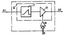
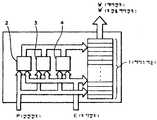
Translated fromKorean종래에는 제7도에 도시된 바와같이 구성된 타이밍신호 지연 회로장치가 제안되어 있는바, 즉 이 장치는 입력타이밍신호(Q1)가 공급되는 논리게이트(1)와. 저항(R)과 가변용량소자(C)로 이루어지는 다수 (n)개의 지연소자(D1∼Dn)가 종속접속되어 상기 논리게이트(1)의 출력측에 접속되어 있는 종속접속회로(G)를 갖추어 구성돼 있다. 여기서 상기 지연소자(D1∼Dn)에 있는 가변용량소자(C)에 관해서는, 상기 종속접속회로(G)에서 실제로 얻는 출력타이밍신호(Q2)의 입력타이밍신호(Q1)에 대한 지연시간의 값과 지연시간의 예정설정값간의 오차량을 나타내게끔 코드화되어 있는 오차정보(E)를 입력으로 하는 D/A 변환회로(B)로 부터의 아날로그제어신호에 의해서 그 용량을 제어함으로써, 종속접속회로(G)로 부터 출력되는 출력타이밍신호(Q2)를 입력타이밍신호(Ql)에 대해서 상기한 예정된 설정값에 가장 가까운 지연시간만큼 지연시켜 출력하도록 되어있다.Conventionally, a timing signal delay circuit device constructed as shown in FIG. 7 has been proposed, i.e., a logic gate 1 to which an input timing signal Q1 is supplied. A resistance (R) and a variable capacitance element (C) a number (n) of delay elements (D1 ~Dn) are cascade-connected slave that is connected to the output side of the logic gate (1) connected to a circuit (G) consisting of It is equipped. Here, with respect to the variable capacitor C in the delay elements D1 to Dn , the delay time with respect to the input timing signal Q1 of the output timing signal Q2 actually obtained by the slave connection circuit G is described. The capacitance is controlled by an analog control signal from the D / A converter circuit B that receives the error information E coded to display the error amount between the value of the value and the predetermined set value of the delay time. The output timing signal Q2 output from the connection circuit G is delayed for the input timing signal Ql by a delay time closest to the predetermined set value and outputted.
또한 종래에는 제8도에 도시된 바와같이 입력타이밍신호(Q1)를 삼각파로 변환시켜 주는 파형변환회로(11)와 이 파형변환회로(11)의 출력측에 접속된 임계치게이트회로(12)로 이루어진 종속접속회로(G)를 구비한 구성으로 되어, 상기 임계치게이트회로(12)의 임계치를 제7도의 경우와 마찬가지인 오차정보(E)를 입력으로 하는 D/A 변환회로(B)로 부터의 아날로그제어신호에 의해서 제어함으로써 종속접속회로(G)로 부터 출력되는 출력타이밍신호(Q2)를 입력타이밍신호(Q1)에 대해서 상기한 예정된 설정값에 가장 가까운 지연시간만큼 지연시켜 출력하도록 된 타이밍신호 지연회로장치도 제안되어 있다.In addition, conventionally, a
발명이 해결하고자 하는 문제점Problems to be Solved by the Invention
그러나 제7도에 도시한 타이밍신호 지연회로장치의 경우, D/A 변환회로(B)가 높은 정밀도로 구성되어있지 않는한 높은 정밀도로 지연된 출력타이밍신호(Q2)를 출력시킬 수가 없을 뿐만 아니라 높은 정밀도로 구성된 D/A 변환회로(B)를 필요로 하고 있으므로 타이밍신호 지연회로장치를 소형고밀도로 반도체집적회로화하는데 어려움을 초래하게 된다고 하는 결정이 있다.However, in the case of the timing signal delay circuit device shown in FIG. 7, the output timing signal Q2 delayed with high precision cannot be output as well as high unless the D / A conversion circuit B is configured with high precision. Since the D / A conversion circuit B configured with precision is required, it has been decided that the timing signal delay circuit device will cause difficulty in miniaturizing and integrating the circuit into the circuit.
또한 제8도에 도시한 타이밍신호 지연회로장치의 경우도 파형변환회로(1l), 임계치게이트회로(12) 및 D/A 변환회로(B)가 높은 정밀도로 구성되어 있지 않는 한 고정밀도로 지여된 출력타이밍신호(Q2)를 출력시킬 수가 없을 뿐만 아니라 높은 정밀도로 구성된 파형변환회로(11)와 임계치게이트회로(12) 및 D/A 변환회로(B)를 필요로 하고 있으므로 제7도의 경우와 마찬가지로 타이밍신호 지연회로장치를 소형고밀도로 반도체집적회로화하는데 어려움을 초래하게 된다고 하는 결점이 있다.Also in the case of the timing signal delay circuit device shown in FIG. 8, the waveform conversion circuit 1l, the
발명의 과제Problem of invention
따라서, 본 발명은 상기한 결점이 없는 새로운 타이밍신호 지연회로장치를 제공함에 그 목적이 있다.Accordingly, an object of the present invention is to provide a new timing signal delay circuit device without the above-mentioned drawbacks.
본 출원의 첫번째 발명에 따른 타이밍신호 지연회로장치는, 타이밍신호에 서로 다른 지연시간을 주는 다수(m)개의 지연소자(D1∼Dm)와, 이들 지연소자(Dl∼Dm)의 입력측 또는 출력측에 접속됨과 동시에 상기 다수(m)개의 지연소자(D1∼Dm)중 하나를 제어정보에 기초해서 선택하는 선택회로를 갖춘 다수(n)개의 지연회로(U1∼Un)가 접속되어 있는 종속접속회로, 출력타이밍신호의 입력타이밍신호에 대한 지연시간의 예정설정값을 나타내고 있는 설정정보와 상기 종속접속회로로 부터 얻어지는 출력타이밍신호의 입력타이밍신호에 대한 지연시간의 값과 상기 설정값과의 차인 오차량을 나타내고 있는 오차정보를 받아서 그들 설정정보및 오차정보의 연산을 하고, 상기 지연회로(U1∼Un)의 선택회로를 제어하는 상기 제어정보를 상기 종속접속회로로 부터 얻는 상기 출력타이밍신호의 상기 입력타이밍신호에 대한 지연시간의 값이 상기 실정값에 가장 가까운 값에서 얻어지도록 발생시키는 연산제어회로를 구비하고 있다.This circuit delays the timing signals according to the first invention of the application apparatus, giving a number of different delay times to a timing signal (m) of delay elements (D1 ~Dm) and, of these delay elements (Dl ~Dm) At the same time the number (m) of the delay elements to the input side or the output side as soon connection (D1 ~Dm) of the delay circuit number (n) with a selection circuit for selecting, based on one of the control information (U1 ~Un) Setting information indicating a predetermined setting value of the delay time for the input timing signal of the slave timing circuit and the output timing signal to which the subordinate connection circuit is connected, and the value of the delay time for the input timing signal of the output timing signal obtained from the slave connection circuit. the calculation of the set values and the five receiving the error information that indicates the vehicle their setup information and error information of the car, and the cascade-connected to the control information for controlling the selection circuit of the delay circuit (U1 ~Un) circuit The value of the delay time for the input timing signals of the timing signal output from the gain and a calculation control circuit to be obtained from the nearest value generated in the situation value.
또한 본 출원의 두번째 발명에 따른 타이밍신호 지연회로장치는 타이밍신호에 서로 다른 지연시간을 주는 다수(m)개의 지연소자(D1∼Dm)와, 이 지연소자(D1∼Dm)의 입력측 또는 출력측에 접속됨과 더불어 상기 다수(m)개의 지연소자(D1∼Dm)중 하나를 제어정보에 의거해서 선택하는 선택회로를 갖춘 다수(n)개의 지연회로(U1∼Un), 상기 타이밍신호에 서로 다른 지연시간을 주는 다수(K)개의 보정용 지연소자(D1'∼Dk'), 그들 보정용 소자(D1'∼Dk')중 하나를 보정용 제어정보에 기초해서 선택하는 보정용 선택회로를 갖춘 1개 (1은 1이상의 정수)의 보정용 지연회로(U1'∼U1')가 종속접속되어 있는 종속접속회로, 출력타이밍 신호의 입력타이밍신호에 대한 지연시간의 예정된 설정값을 나타내고 있는 설정정보와 상기 종속접속회로에서 얻어지는 출력 타이밍신호의 입력타이밍신호에 대한 지연시간의 값과 상기 설정정보와의 오차량을 나타내고 있는 오차정보를 받아서 그들 설정정보 및 오차정보의 연산을 하고, 상기 지연회로(U1∼Un)의 선택회로를 제어하는 상기 제어정보 및 상기 보정용 지연회로(U1∼Un)의 선택회로를 제어하는 보정용 제어정보를 상기 종속접속회로로 부터 얻는 상기 출력타이밍신호의 상기 입력타이밍신호에 대한 지연시간의 값이 상기 설정값에 가장 가까운 값에서 얻어지도록 발생시키는 연산제어회로를 구비하고 있다.A delay circuit timing signal according to the second aspect of the invention apparatus of the number (m) of delay elements (D1 ~Dm) and delay elements (D1 ~Dm) giving a different delay time in the timing signal in addition to the input side or the output side as soon connected to a plurality (m) of delay elements (D1 ~Dm) one of the control information to the delay with a selection circuit for selecting a number (n) of the circuit based on the (U1 ~Un) One of a plurality (K) of correction delay elements (D1 'to Dk ') and one of these correction elements (D1 'to Dk ') that give different delay times to the timing signal is based on correction control information. with a correction selection circuit for selecting one of the connected dependent correction delay circuits (U1 '~U1') is dependent on (1 is an integer of 1 or more) connection circuit, the delay time for the input timing signals of the output timing signal Setting information indicating a predetermined setting value and output obtained from the slave connection circuit. Receive the error information indicating the value of the delay time with respect to the input timing signal of the output timing signal and the error amount of the setting information, and calculate the setting information and the error information, and calculate the values of the delay circuits U1 to Un . Delay time for the input timing signal of the output timing signal for obtaining the control information for controlling the selection circuit and the control information for controlling the selection circuit of the correction delay circuits U1 to Un from the slave connection circuit. An arithmetic control circuit is generated so that the value of is obtained from the value closest to the set value.
상기한 첫번째의 발명에 따른 타이밍신호 지연회로장치에 의하면, 지연회로(U1∼Un)의 각각에 있어서 지연소자(D1∼Dm)중 하나는 그의 선택회로에 의해 선택되는바, 전체로서 n개의 지연회로가 각각 타이밍신호에 주는 지연시간의 합의 지연시간만큼 입력타이밍신호에 대해서 지연된 출력타이밍신호를 종속접속회로에서 출력시킬 수 있으므로 타이밍신호 지연회로장치로서의 기능이 얻어지게 된다.According to the timing signal delay circuit device according to the first invention described above, in each of the delay circuits U1 to Un , one of the delay elements D1 to Dm is selected by its selection circuit. As a result, since the output timing signal delayed with respect to the input timing signal can be output from the slave connection circuit by the delay time sum of the delay time which the n delay circuits respectively give to the timing signal, the function as the timing signal delay circuit device is obtained.
그리고 이 경우 지연회로(U1∼Um)의 지연소자(D1∼Dm)의 각각이 타이밍신호에 주는 지연시간이 미리 적당하게 선정되어 있으면, 그들의 지연시간이 특히 높은 정밀도에 있지 않아도 또 지연회로(U1∼Un)의 지연소자(D1∼Dm)가 높은 정밀도로 구성되어 있지 않아도 높은 정밀도인 지연시간으로 지연시킨 출력타이밍신호를 출력시킬 수가 있다.In this case, if the delay time given to the timing signal by each of the delay elements D1 to Dm of the delay circuits U1 to Um is appropriately selected in advance, even if the delay time is not particularly high accuracy, Evenif the delay elements D1 to Dm of the delay circuits U1 to Un are not configured with high precision, an output timing signal delayed with a high precision delay time can be output.
또한 이와같이 지연회로(U1∼Un)의 지연소자(D1∼Dm)가 높은 정밀도로 구성되어 있지 않아도 좋으므로 지연회로(U1∼Un)의 선택회로 및 연산제어회로도 쉽게 반도체집적회로화 할 수 있어 타이밍신호 지연회로장치를 소형고밀도로 쉽게 반도체집적회로화할 수 있다.Also in this way a delay circuit (U1 ~Un) delay elements (D1 ~Dm) is so good does not need to be configured with high accuracy selection of the delay circuit (U1 ~Un) circuit and an operation control circuit diagram of the semiconductor integrated easily Since the circuit can be circuitized, the timing signal delay circuit device can be easily semiconductor integrated circuit with small size and high density.
뿐만 아니라 본원 첫번째의 발명에 따른 타이밍신호 지연회로장치에 있어서, 전술한 설정값의 예정된 설정분해능을 Td, 제j번째의 지연회로(Uj,: j=1,2… ,n)에 있어서의 제i번째의 지연소자(Di, :1=1,2,…,m)가 상기 타이밍신호에 주는 지연시간을 Tij라 할때,In addition, in the timing signal delay circuit device according to the first invention of the present application, the predetermined setting resolution of the above-described setting value is set in Td , the j th delay circuit Uj ,: j = 1, 2..., N. the i-th delay elements of: when(d i, 1 = 1,2, ..., m) is the delay time that the timing signal Tij d,
Tij=Tdㆍ(i-1)·mj-1........................................................... (1)Tij = Td ㆍ (i-1) mj-1 ... ......................... (One)
의 관계를 만족하면, 각 지연소자가 타이밍신호에 주는 지연시간에 절대오차를 가지고 있어도 상대오차가 없는 경우, 설정분해능의 값과 절대오차의 값과의 합에서 그의 합의 값인 도약시간간격을 순차 등간격으로 취한 다수의 값중 소망의 하나의 값만큼 지연시간이 부여된 출력타이밍신호를 출력시킬 수 있다.When the relationship is satisfied, if there is no relative error even though each delay element has an absolute error in the delay time given to the timing signal, the leap time interval that is the sum of the sum of the set resolution value and the absolute error value is sequentially added. It is possible to output an output timing signal given a delay time by a desired one of a plurality of values taken at intervals.
또 본원 첫번째의 발명에 따른 타이밍신호 지연회로장치에 있어서, 전술한 설정값의 예정된 설정분해능을 Td, 제j번째의 지연회로(Uj: j=1,2…,n)에 있어서의 제i번째의 지연소자(Di, i=1,2,…,m)가 타이밍신호에 주는 지연시간을 Tij, 그 지연시간(Tij)의 상대오차율의 절대값을 e라 할때, 지연시간(Tij)이Further, in the timing signal delay circuit device according to the first aspect of the present application, the predetermined setting resolution of the above-described setting value is set to Td , and the first time in the j th delay circuit (Uj : j = 1, 2..., N). The delay time given by the i-th delay element (Di , i = 1, 2, ..., m) to the timing signal is Tij and the absolute value of the relative error rate of the delay time Tij is e. Time (Tij )

의 관계를 만족하고 있으면, 각 지연소자가 타이밍신호에 주는 지연시간에 상대오차를 가지고 있어도 설정분해능의 값과 상대오차와의 합에서 그 합의 값인 도약시간간격을 순차적으로 취한 다수의 값중 소망의 하나의 값만큼 지연시간이 부여된 출력타이밍신호를 출력시킬 수 있다.If the relationship is satisfied, one of the desired values among the values obtained by sequentially taking the leap time interval that is the sum of the set resolution value and the relative error even though each delay element has a relative error in the delay time given to the timing signal. The output timing signal given the delay time can be output as much as.
또한 본원 두번째의 발명에 따른 타이밍신호 지연회로장치에 의하면, 지연회로(U1∼Un)의 각각에 있어서, 지연소자(D1∼Dm)중 하나는 그의 선택회로에 의해 선택되는 바, 전체로서 n개의 지연회로가 각각 타이밍신호에 주는 지연시간의 합과 보정용 지연회로(U1'∼U1')의 각각에 있어서, 보정용 지연소자(D1'∼Dk')중 하나는 그의 선택회로에 의해 선택되는바, 전체로서 1개의 보정용 지연소자가 각각 타이밍신호에 주는 지연시간의 합과의 합만큼 입력타이밍신호에 대해서 지연된 출력타이밍신호를 종속접속회로에서 출력시킬 수가 있으므로 본원 첫번째의 발명에 따른 타이밍신호 지연회로장치의 경우와 마찬가지로 타이밍신호 지연회로장치로서의 기능이 얻어지게 된다.Further, according to the timing signal delay circuit device according to the second invention of the present application, in each of the delay circuits U1 to Un , one of the delay elements D1 to Dm is selected by the selection circuit thereof. in each of a total n number of delay circuits, each delay time set and the correction delay circuits (U1 '~U1') of which a timing signal, one of the correction delay elements (D1 '~Dk') is his Selected by the selection circuit, as a whole, the output timing signal delayed with respect to the input timing signal can be output from the slave connection circuit by the sum of the delay time given to each timing signal by one correction delay element. As in the case of the timing signal delay circuit device according to the invention, the function as the timing signal delay circuit device is obtained.
그리고 이 경우도 본원 첫번째의 발명에 따른 타이밍신호 지연회로장치의 경우와 마찬가지로 지연회로(U1∼Un)의 지연소자(D1∼Dm)의 각각이 타이밍신호에 주는 지연시간 및 보정용 지연회로(U1'∼U1')의 보정용 지연소자(D1'∼Dk')의 각각이 타이밍신호에 주는 지연시간이 미리 적당하게 선택되어 있으면, 그들의 지연시간이 특히 높은 정밀도를 갖지 않아도, 또 지연회로(U1∼Un)의 지연소자(D1∼Dm) 및 보정용 지연회로(U1'∼U1')의 보정용 지연소자(D1'∼Dk')가 높은 정밀도로 구성되어 있지 않아도 높은 정밀도의 지연시간으로 지연된 출력타이밍신호를 출력시킬 수가 있다.Also in this case, as in the case of the timing signal delay circuit device according to the first invention of the present application, the delay time and the correction delay given to the timing signal by each of the delay elements D1 to Dm of the delay circuits U1 to Un . circuits (U1 '~U1') for correcting the delay elements (D1 '~Dk') each of which, if the delay time that the timing signal is suitably selected in advance, their delay times do not have a particularly high accuracy of the , and delay circuit delay elements of(U 1 ~U n) (D 1 ~D m) and the correction delay circuits (U1 '~U1') for correcting the delay elements (D1 '~Dk') the high accuracy of the It is possible to output the delayed output timing signal with a high precision delay time even if it is not configured.
더구나 본원 두번째의 발명에 따른 타이밍신호 지연회로장치의 경우, 지연회로(U1∼Un)이외의 보정용 지연회로(U1'∼U1')를 가지므로 본원 첫번째의 발명에 따른 타이밍신호 지연회로 장치보다도 한결 높은 정밀도의 지연시간으로 지연시킨 출력타이밍신호를 출력시킬 수 있다.Moreover, the present case the timing signal delay circuit according to the invention of the second delay circuit (U1 ~Un) other than the correction delay circuits (U1 '~U1') because of the delayed timing signal according to the first invention of the present application It is possible to output the output timing signal delayed with a higher accuracy delay time than the circuit arrangement.
또한 본원 두번째의 발명에 따른 타이밍신호 지연회로장치의 경우 본원 첫번째의 발명에 따른 타이밍신호 지연회로장치의 경우와 마찬가지로 지연회로(U1∼Un)의 지연소자(D1∼Dm) 및 보정용 지연회로(U1'∼U1')의 보정용 지연소자(D1'∼D1')가 높은 정밀도로 구성되어 있지 않아도 좋으므로, 또 지연회로(U1∼Un) 및 보정용 지연회로(U1'∼U1')의 선택회로와 연산제어회로도 용이하게 반도체집적회로화할 수 있으므로 타이밍신호 지연회로장치를 소형고밀도로 쉽게 반도체집적회로화할 수 있다.In addition, in the case of the timing signal delay circuit device according to the second invention of the present application, the delay elements D1 to Dm and the correction delay of the delay circuits U1 to Un are the same as in the timing signal delay circuit device according to the first invention of the present application. Since it is fine circuit (U1 '~U1') for correcting the delay elements (D1 '~D1') of does not need to be configured with high accuracy, and a delay circuit (U1 ~Un) and the correction delay circuit (USince the selection circuit of1 'to U1 ' and the operation control circuit can be easily integrated into a semiconductor integrated circuit, the timing signal delay circuit device can be easily integrated into a small, high density circuit.
더욱이 본원 두번째의 발명에 따른 타이밍신호 지연회로장치에 있어서, 상기한 설정값의 예정된 설정분해능을 Td, 제j번째의 지연회로(Uj, j=1,2,…,n)에 있는 제i번째의 지연소자(D1,i=1,2·…,n)가 상기 타이밍신호에 주는 지연시간을 Tij라 할때 상기한 (1)식의 관계를 만족하고, 또 제 β번째의 보정용 지연소자(Uβ' : β=1,2,…,l)에 있는 제α번째의 보정용 지연소자(Dα: α=1,2,…,k)가 타이밍신호에 주는 지연시간을 Tαβ라 할때Furthermore, in the timing signal delay circuit device according to the second invention of the present application, the predetermined setting resolution of the set value is defined as Td , the j th delay circuit Uj , j = 1, 2,... When the delay time given to the timing signal by the i-th delay element (D1 , i = 1, 2..., n) is Tij , the above relation (1) is satisfied, and The delay time given to the timing signal by the α-th correction delay element (Dα: α = 1, 2, ..., k) in the correction delay element Uβ ': β = 1, 2, ..., l is referred to as Tαβ. time
Tαβ==Tdㆍ(α-1)·Kβ-1........................................... (3)Tαβ == Td ㆍ (α-1) · Kβ-1 ........................ ......... (3)
의 관계를 만족하면, 각 지연소자 및 각 보정용 지연소자가 타이밍신호에 주는 지연시간에 상대오차를 갖고 있어도 본원 첫번째의 발명에 따른 타이밍신호 지연회로장치에 있어서 상기한 (2)식의 관계를 만족하고있는 경우와 마찬가지로 설정분해능과 상대오차와의 합에서 그 합의 값인 도약시간간격을 순차적으로 취한 다수의 값중 바라는 하나의 값만큼 지연시간이 부여된 출력타이밍신호를 출력시킬 수가 있다.When the relationship is satisfied, even if each delay element and each correction delay element has a relative error in the delay time given to the timing signal, the above relationship (2) is satisfied in the timing signal delay circuit device according to the first aspect of the present application. As in the case of the above case, the output timing signal given the delay time by one desired value can be output from the sum of the set resolution and the relative error.
본 발명은 타이밍신호를 소정의 값으로 설정된 지연시간만큼 지연시켜 주도록 타이밍신호 지연회로장치에 관한 것이다.The present invention relates to a timing signal delay circuit device for delaying a timing signal by a delay time set to a predetermined value.
제1도는 본원 첫번째의 발명에 따른 타이밍신호 지연회로장치의 실시예를 도시한 계통적 접속도.1 is a systematic connection diagram showing an embodiment of a timing signal delay circuit device according to the first invention of the present application.
제2도는 제1도에 도시된 각 지연회로(U1∼U3)의 지연소자(D1∼D4)의 실시예를 도시한 접속도.FIG. 2 is a connection diagram showing an embodiment of the delay elements D1 to D4 of the delay circuits U1 to U3 shown in FIG.
제3도 및 제4도는 제1도에 도시한 본 발명에 따른 타이밍신호 지연회로창치에 있는 지연회로(Uj: j=1,… ,3)의 지연소자(D1: i=1,…,4)가 타이밍신호에 대해서 부여해 주는 지연시간을 나타낸 도면.3 and 4 show the delay elements D1 : i = 1,... Of the delay circuit Uj : j = 1,..., 3 in the timing signal delay circuit window according to the present invention shown in FIG. Fig. 4 shows the delay time given to the timing signal.
제5도는 본원 두번째의 발명에 따른 타이밍신호 지연회로장치의 실시예를 도시한 계통적 접속도.5 is a systematic connection diagram showing an embodiment of a timing signal delay circuit device according to the second invention of the present application.
제6도는 제5도에 도시한 지연회로(U1∼U3)의 지연소자(D1∼D4) 및 지연회로(U')의 지연소자(D1'∼D4')가 타이밍신호에 대해서 부여해 주는 지연시간을 나타낸 도면.6 is a timing signal of delay elements D1 to D4 of delay circuits U1 to U3 and delay elements D1 'to D4 ' of delay circuit U 'shown in FIG. A diagram showing the delay time given for.
제7도 및 제8도는 종래의 타이밍신호 지연회로장치를 도시한 계통적 접속도.7 and 8 are systematic connection diagrams showing a conventional timing signal delay circuit device.
제9도는 본 발명에 있어서 연산제어회로의 1실시예를 도시한 기능블록도이다.9 is a functional block diagram showing one embodiment of the operation control circuit in the present invention.
다음에 제1도를 참조해서 첫번째의 발명에 따른 타이밍신호 지연회로장치의 실시예를 설명한다.Next, an embodiment of a timing signal delay circuit device according to the first invention will be described with reference to FIG.
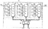
제1도에 도시한 첫번째의 발명에 따른 타이밍신호 지연회로 장치는 다수(n)개 예컨대 3개의 지연회로(U1∼Un; n=3)가 종속접속되어 있는 종속접속회로(G)를 갖추고 있다.The timing signal delay circuit device according to the first invention shown in FIG.1 has a slave connection circuit G in which a plurality (n) of three delay circuits U1 to Un ; n = 3 are cascaded. Equipped.
그중 지연회로(Uj; j=1,2,…,n(=3))는 각각 타이밍 신호에 서로 다른 지연시간을 주는 다수(m)개, 예컨대 4개의 지연소자(D1∼Dm; m=4)와 그들 지연소자(D1∼D4)의 예컨대 출력측에 접속됨과 더불어 다수(m)개 (이 경우 4개)의 지연소자(D1∼D4)중의 하나를 후술하는 연산제어회로(M)로 부터의 제어정보에 의거해 선택하는 선택회로(S)를 갖추고 있다.Among them, a delay circuit(U j; j = 1,2, ..., n (= 3)) has a number (m) one, for example, four delay elements (D1 ~Dm giving a different delay time for each of the timing signals; m = 4) and the output control of the delay elements D1 to D4 , for example, and the arithmetic control which describes one of a plurality (m) of delay elements D1 to D4 described later. A selection circuit S for selecting on the basis of control information from the circuit M is provided.
한편, 지연회로(Uj)에 있는 지연소자(Dj; i=1,2,… ,m(=4))로서는 예컨대 제2도에 도시한 바와같은 낸드게이트(21)를 이용한 전송시스템이 이용되고, 이 전송시스템은 그의 배선용량(22), 바이폴라트랜지스터의 베이스. 컬렉터사이 용량을 이용하는 용량소자(23), 바이폴라트랜지스터의 베이스. 에미터사이의 용량을 이용하는 용량소자(24)등이 접속되어 있는 구성을 갖춘 하나 이상의 시스템을 이용해서 얻어진다.On the other hand, as a delay element (Dj ; i = 1, 2, ..., m (= 4)) in the delay circuit Uj , a transmission system using the
또한 제1도에 도시한 첫번째의 발명에 따른 타이밍신호 지연회로장치는 지연회로(U1∼U3)의 선택회로(S)를 제어하는 연산제어회로(M)를 갖추고 있다.Further, the timing signal delay circuit device according to the first invention shown in FIG. 1 is provided with an operation control circuit M for controlling the selection circuit S of the delay circuits U1 to U3 .
상기 연산제어회로(M)는 종속접속회로(G)로 부터 얻어지는 출력타이밍신호(Q2)의 입력타이밍신호(Ql)에 대한 지연시간의 예정된 설정값(이것을 Tp라 한다)을 나타내고 있는 설정정보(이것을 P라 한다)와, 종속접속회로(G)로 부터 실제로 얻어지는 출력타이밍신호(Q2)의 입력타이밍신호(Q1)에 대한 지연시간(이것을 TR이라 한다)의 값과 상기한 설정값(Tp)과의 오차량을 나타내고 있는 오차정보(E)의 연산을 한다.The operation control circuit M is setting information indicating a predetermined set value of the delay time for the input timing signal Ql of the output timing signal Q2 obtained from the slave connection circuit G (this is referred to as Tp ). (This is called P), the value of the delay time (this is called TR ) for the input timing signal Q1 of the output timing signal Q2 actually obtained from the slave connection circuit G, and the above-described setting value ( Calculate the error information E representing the amount of error with Tp ).
즉, 제9도에 도시한 것저럼 오차정보(E)를 받아서 설정정보(P) 및 오차청보(E)간의 연산을 하고, 지연회로(U1~U3)의 선택회로(S)를 제어하는 제어정보(W1~W3)를 종속접속회로(G)에서 얻어지는 출력 타이밍 신호(Q2)의 입력타이밍신호(Q1)에 대한 지연시간(TR)의 값이 상기한 설정값(Tp)에 가장 가까운 값에서 얻어지도록 발생시키게 된다.That is, as shown in FIG. 9, the error information E is received, the operation is performed between the setting information P and the error notification E, and the selection circuit S of the delay circuits U1 to U3 is controlled. control information (W1 ~ W3) a cascade-connected circuit (G) the value of the delay time (TR) on the input timing signal (Q1) of the resulting output timing signal (Q2) the set at a value (Tp that ) To be obtained at the value closest to
이상 본원 첫번째의 발명에 따른 타이밍신호 지연회로장치의 실시예의 구성이다.The configuration of the embodiment of the timing signal delay circuit device according to the first invention of the present application has been described above.
상기한 구성을 갖춘 본원 첫번째의 발명에 따른 타이밍신호 지연회로장치에 의하면, 지연회로(U1∼U3)의 각각에 있어서, 그의 선택회로(S)에 의해서 선택된 지연소자(D1∼D4)중의 하나로 이루어져 전체로서 3개인 지연소자가 각각 타이밍신호에 부여되는 지연시간의 합의 값으로 되어 상기한 설정값(Tp)에 가장 가까운 지연시간(TR)만큼 입력타이밍신호(Ql)에 대해서 지연시키고 있는 출력타이밍신호를 종속접속회로(G)로 부터 출력시킬 수 있다.According to the timing signal delay circuit device according to the first invention of the present invention having the above-described configuration, in each of the delay circuits U1 to U3 , the delay elements D1 to D4 selected by the selection circuit S thereof. The delay time TR closest to the set value Tp , and the input timing signal Ql The delayed output timing signal can be output from the slave connection circuit (G).
즉, 지금 지연회로(Uj:j=1,2,…,n(=3))에 있어서의 지연소자(Dl: i=1,2,… ,m(=4))가 타이밍신호에 주는 지연시간을 Tij라 할때, 지연회로(U3)에 있어서 예컨대 지연소자(D2)를 선택회로(S)에 의해 제어정보(W1)의 내용에 의거해서 선택하고 ; 또 지연회로(U2)에 있어서 예컨대 지연소자(D1)를 제어정보(W2)의 내용에 기초해서 선택회로(S)에 의해 선택하며 ; 지연회로(U3)에 있어서 예컨대 지연소자(D3)를 선택회로(S)에 의해 제어정보(W3)의 내용에 의거해서 선택하게 되면,In other words, the delay elements Dl : i = 1, 2, ..., m (= 4) in the delay circuit Uj : j = 1, 2, ..., n (= 3) are applied to the timing signal. When the delay time is Tij , the delay circuit U3 selects, for example, the delay element D2 by the selection circuit S based on the contents of the control information W1 ; In the delay circuit U2 , for example, the delay element D1 is selected by the selection circuit S based on the contents of the control information W2 ; In the delay circuit U3 , for example, when the delay element D3 is selected by the selection circuit S based on the contents of the control information W3 ,
TR= T21+T12+ T33TR = T21 + T12 + T33
으로 표현되는 지연시간(TR)만큼 입력타이밍신호(Q1)에 대해서 지연시킨 출력타이밍신호(Q2)를 상기한 설정값(Tp)에 가장 가까운 지연시간만큼 입력타이밍신호(Q1)에 대해서 지연시킨 출력타이밍신호로서 출력시킬 수 있게 된다. 따라서 제1도에 도시한 본원 첫번째의 발명에 따른 타이밍신호 지연회로장지에 의하면 타이밍신호 지연회로장치로서의 기능이 얻어지게 된다.The output timing signal Q2 , which is delayed with respect to the input timing signal Q1 by the delay time TR expressed by, is applied to the input timing signal Q1 by the delay time closest to the set value Tp . The output timing signal can be output as a delayed output timing signal. Therefore, according to the timing signal delay circuit device according to the first invention shown in FIG. 1, the function as the timing signal delay circuit device is obtained.
그리고 이 경우 출력타이밍신호(Q2)를 상기한 지연시간이 주어진 것으로서 종속접속회로(G)로 부터 출력시킬 수 있으므로 지연회로(U1)의 지연소자(D1∼D4), 지연회로(U2)의 지연소자(D1∼D4), 지연회로(U3)의 지연소자(D1∼D4)가 각각 타이밍신호에 주는 지연시간(T11∼T41, T12∼T42, T13∼T43)이 미리 적당하게 선택되어 있으면 그들 지연시간이 특히 높은 정밀도가 아니어도, 또 지연회로(U1∼U3)의 지연소자(D1∼D4)가 높은 정밀도로 구성되어 있지 않아도, 높은 정밀도의 지연시간으로 지연시킨 출력타이밍신호(Q2)를 종속접속회로(G)로 부터 출력시킬 수 있게 된다.And delay elements (D1 ~D4) in this case, because the delay is a delay time of the output timing signal (Q2) can be output dependent from the connection circuit (G) as given circuit (U1), a delay circuit (U2) delay elements (D1 ~D4), delay elements (D1 ~D4) the delay time(T 11 ~T 41, T 12 ~T 42 to each timing signal of the delay circuit (U3) of, If T13 to T43 are appropriately selected in advance, the delay elements D1 to D4 of the delay circuits U1 to U3 are configured with high precision even if their delay times are not particularly high precision. If not, the output timing signal Q2 delayed with a high precision delay time can be output from the slave connection circuit G.
또한 상기한 바와같이 지연회로(U1∼U3)의 지연소자(D1∼D4)가 높은 정밀도로 구성되어 있지 않아도 좋으므로, 또 지연회로(U1∼U3)의 선택회로(S) 및 연산제어회로(M)도 쉽게 반도체집적회로화할 수 있으므로, 타이밍신호 지연회로장치를 소형고밀도로 용이하게 반도체집적회로화할 수 있게 된다.A delay circuit (U1 ~U3) delay elements (D1 ~D4) is so good does not need to be configured with high accuracy, and a delay circuit (U1 ~U3) the selection circuit (S, as described above for the ) And the operation control circuit M can be easily integrated into a semiconductor integrated circuit, so that the timing signal delay circuit device can be easily integrated into a small, high density circuit.
더구나 제1도에서 상술한 첫번째의 발명에 따른 타이밍신호 지연회로장치에 있어서, 상기한 설정값(Tp)의 예정된 설정분해능을 Td라 하고, 또 지연회로(Uj)의 지연소자(Di)가 타이밍 신호에 주는 지연시간을 상기한 바와같이 Tij라 할때 그의 지연시간(Tij)이 상기한 (1)식과 같이Furthermore, in the timing signal delay circuit device according to the first invention described above in FIG. 1, the predetermined setting resolution of the set value Tp is referred to as Td , and the delay element D of the delay circuit Uj .When i ) is a delay time given to the timing signal as Tij , the delay time Tij is represented by the above equation (1).
Tij=Tdㆍ(i-1)ㆍmj-l........................................................... (4)Tij = Td ㆍ (i-1) mjl ... ....................... (4)
의 관계를 만족하도록 지연회로(Uj)의 지연소자(D1)를 구성시키게 된다.The delay element D1 of the delay circuit Uj is configured to satisfy the relationship of.
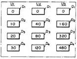
즉, 예컨대 상기한 설정분해능(Td)을 10PS(pico 秒)라 할때, 지연회로(Uj)의 지연소자(Dl)를 그것이 타이밍신호에 주는 지연시간(Tij)으로 인하여 상기한 (4)식에 의거해서 제3도에 도시한 값의 지연시간(PS)이 얻어지도록 구성시키게 된다. 이때는 종속접속회로(G)에서 얻어지는 출력타이밍신호(Q2)의 입력타이밍신호(Q1)에 대한 최대지연시간(Tmax)이 Tmax=Tdㆍ(mn-1) ............................. (5)That is, for example, when the set resolution Td is 10 PS (pico co), the delay time Tij which gives the delay element D1 of the delay circuit Uj to the timing signal is described above. Based on equation (4), the delay time PS of the value shown in FIG. 3 is obtained. At this time, the maximum delay time Tmax for the input timing signal Q1 of the output timing signal Q2 obtained in the slave connection circuit G is Tmax = Td ㆍ (mn -1) ..... ....................... (5)
으로 주어지는데, 지연회로(U1∼U3)의 지연소자(Dl∼D4)의 각각이 타이밍신호에 주는 지연시간에 절대오차(이것을 Te라 한다)를 갖추고 있다해도 상대오차(이것을 Tc라 한다)를 갖고 있지 않은 경우, 상기한 설정분해능(Td)의 값과 절대오차(Te)의 값과의 합(Td+Te)에서 상기한 최대지연시간(Tmax)을 주는 (5)식의 우변 Td를 (Td+Te)로 치환해서 얻어지는 (Td+Te)ㆍ(mn-1)까지의 사이에 있어서, 합(Td+Te)의 값인 도약시간(이것을 Tq라 한다)의 간격을 순차 등간격으로 취한 다수의 값(Tq,2Tq,3Tq,…·)중의 하나의 값만큼 지연시간이 부여된 출력타이밍신호(Q2)를 종속접속회로(G)로부터 출력시킬 수 있다.Although each of the delay elements D1 to D4 of the delay circuits U1 to U3 has an absolute error (referred to as Te ) in the delay time given to the timing signal, the relative error (this is Tc ), the maximum delay time (Tmax ) described in the sum (Td + Te ) of the value of the set resolution (Td ) and the value of the absolute error (Te ). 5, the right-hand side of Td (Td +e T) (Td + Te) and (mn -1) in between, (Td + Te) of the sum to be obtained by replacing in the expression giving the Output timing signal Q2 given a delay time by one of a plurality of values (Tq , 2Tq , 3Tq ,… ·) taking the interval of the leap time (this is called Tq ) at equal intervals sequentially ) Can be output from the slave connection circuit (G).
예컨대 상기한 설정분해능(Td)을 10PS라 하고, 지연회로(Uj)의 지연소자(Dl)를 그것이 타이밍신호에 주는 지연시간(Tij)으로 하여금 제3도에 도시한 값의 지연시간이 얻어지도록 구성시킨 경우에 있어서, 상기한 절대오차(Te)가 각 지연소자가 타이밍신호에 주는 지연시간에 대해 ±10%이라 하면, 순차 등간격으로 취한값[Tq(=10±1)), 2Tq(=2(10±l), 3Tq(=(10±1)),…·]중의 소망의 하나의 값만큼 지연시간이 부여된 출력타이밍신호(Q2)를 종속접속회로(G)로부터 출력시킬 수 있다.For example, the set resolution Td is 10 PS, and the delay time Tij which gives the delay element D1 of the delay circuit Uj to the timing signal causes the delay of the value shown in FIG. In the case where the time is obtained, if the absolute error Te is ± 10% of the delay time given to each timing element by each delay element, the values taken at sequential intervals [Tq (= 10 ± 1)), 2Tq (= 2 (10 ± l), 3Tq (= (10 ± 1)),… ·]] slave connection of output timing signal Q2 given delay time by one of the desired values It can output from the circuit G.
더구나 지연회로(Uj)에 있는 지연소자(D1)의 지연시간(Tij)이 상기한(4)식의 관계를 만족하도록 구성된 경우에 있어서, 각 지연소자가 타이밍신호에 주는 지연시간에 상대오차(Tc)를 가진 경우에는 출력타이밍신호(Q2)에 주는 지연시간의 값은 상기한 도약시간(Tq)의 값에서 순차 등간격으로 취한 다수의 값중에서 얻은 하나의 값으로 되지 않고 설정분해능(Td)과 상대오차(Tc)와의 합(Td+Tc)에서 상기한 최대지연시간(Tmax)을 주는 (5)식의 우변 Td를 (Td+Tc)로 치환해서 얻어지는 (Td+Tc)ㆍ(mn-1)까지의 사이에 있어서, 상기한 도약시간(Tq)보다도 큰 도약시간의 간격을 써서 순차 부등간격으로 취한 다수의 값중에서 취한 하나의 값으로 된다. 그러므로 이 경우의 최대도약시간(이것을 Tm이라 한다)은 지연시간(Tij)의 상대오차율의 절대값(e)을 곱한Furthermore, in the case where the delay time Tij of the delay element D1 in the delay circuit Uj is configured to satisfy the above relationship (4), the delay time that each delay element gives to the timing signal In the case of having a relative error (Tc ), the value of the delay time given to the output timing signal (Q2) does not become a value obtained from a plurality of values taken at equal intervals sequentially from the value of the hopping time (Tq ). In the sum of the set resolution (Td ) and the relative error (Tc ) (Td + Tc ), the right side Td of (5) giving the maximum delay time (Tmax ) is (Td + Tc ) Between (Td + Tc ) · (mn -1) obtained by substituting for a step, taking a plurality of values taken at sequential inequal intervals using an interval of hopping time greater than the above hopping time (Tq ). Is one value. Therefore, the maximum leap time in this case (this is called Tm ) is multiplied by the absolute value (e) of the relative error rate of the delay time (Tij ).
Tm=eㆍTd(2mn-2mn-1-1) ........................................................... (6)Tm = e andT d (2m n -2m n- 1 -1) ................................ ........................... (6)
으로 주어지게 된다.Is given by.
또한, 제1도에서 상술한 본원 첫번째의 발명에 따른 타이밍신호 지연회로장치에 있어서, 지연회로(Uj)의 지연소자(Di)를 상기한 지연시간(Tij)이 작용효과의 항에서 상세히 설명한 (2)식과 마찬가지로,Further, in the timing signal delay circuit device according to the first aspect of the present invention described above with reference to FIG. 1, the delay time Tij in which the delay element Di of the delay circuit Uj isdefined in terms of the effect of operation. As in the formula (2) described in detail,

의 관계를 만족하도록 구성시키게 된다. 예컨대 최대행수가 4행인 경우 T21의 결정에서는 (7)식의 우변 제1항은 (1-e)T11=0으로 되므로,It is configured to satisfy the relationship of. For example, when the maximum number of rows is four, in the determination of T21 , the right side term in the equation (7) becomes (1-e) T11 = 0,
(1+e) T2l≒Td로부터(1 + e) from T2l ≒ Td
T2l≒Td/(1+e)로 결정할 수 있고, 마찬가지로T2l ≒ Td / (1 + e), and likewise
(1+e) T31≒ (1-e) T21+Td로부터(1 + e) from T31 ≒ (1-e) T21 + Td
T31≒2/(1+e)ㆍT21,T31 ≒ 2 / (1 + e) T21 ,
(1+e)T41≒(1-e)T31+Td로부터From (1 + e) T41 ≒ (1-e) T31 + Td
T41≒(1-e)/(1+e)ㆍT31+T21,T41 ≒ (1-e) / (1 + e) T31 + T21 ,
(1+e)T22≒(1-e) (T41+T12) +Td로부터From (1 + e) T22 ≒ (1-e) (T41 + T12 ) + Td
T22≒(1-e)/(1+e)ㆍ(T41+0)+T21, …T22 ≒ (1-e) / (1 + e) · (T41 +0) + T21 ,.
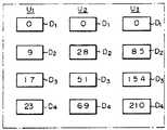
이 되도록 지연시간이 적은 지연소자로부터 순차 지연시간을 결정하면 좋다. 즉, 예컨대 상기한 설정분해능(Td)을 10PS라 할때 지연회로(Uj)의 지연소자(Di)를 그것이 타이밍신호에 주는 지연시간(Tij)으로 하여금 상기한(7)식에 기초해서 제4도에 도시한 값의 지연시간(PS)이 얻어지도록 구성시키게 된다.It is sufficient to determine the sequential delay time from the delay elements having a low delay time. That is, for example, when the set resolution Td is 10 PS, the delay time Tij which gives the delay element Di of the delay circuit Uj to the timing signal is given by the above equation (7). On the basis of this, the delay time PS of the value shown in Fig. 4 is obtained.
이때에는 종속접속회로(G)에서 얻어지는 출력타이밍신호(Q2)의 입력타이밍신호(Ql)에 대한 최대지연시간(Tmax)은 상대오차율(±e)을 가진 것으로부터 ε=(l-e)/(1+e)라할때,At this time, the maximum delay time Tmax with respect to the input timing signal Ql of the output timing signal Q2 obtained from the slave connection circuit G is ε = (le) / ( 1 + e),
[ { (1-ε )m/(l-ε )m} - 1]ㆍTd

으로 주어지는데, 지연회로(U1∼U3)의 지연소자(D1∼D4) 각각이 타이밍신호에 주는 지연시간에 상대오차를 갖고있어도 상기한 설정분해능(Td)의 값과, 그것에 상대오차율(e)을 곱한 값(eㆍTd)과의 합(1+e)Td로부터 적어도 (8)식에 표시된 최대지연시간(Tmax)의 최소값[{(1-ε)m/(1-ε)}n-1ㆍTd까지의 사이에 있어서, (1+e)Td의 값인 도약시간(이것을 Td'라 한다)의 간격을 순차 등간격으로 취한 다수의 값(T'q), 2T'q, 3T'q,…)중 소망의 하나의 값만큼 지연시간이 부여된 타이밍신호(Q2)를 종속접속회로(G)로부터 출력시킬 수있다.Although each of the delay elements D1 to D4 of the delay circuits U1 to U3 has a relative error in the delay time given to the timing signal, the value of the above-described setting resolution Td , and The minimum value of the maximum delay time (Tmax ) expressed in at least (8) from the sum (1 + e) Td multiplied by the relative error rate (e) (e · Td ) [{(1-ε)m / (1-ε)} A number of values (T) in which the interval between the leap time (this is called Td '), which is a value of (1 + e) Td , is taken at equal intervals sequentially betweenn −1 · Td . 'q ), 2T'q , 3T 'q ,... Can output the timing signal Q2 given the delay time by the desired one of the subordinate connection circuits G).
연산제어회로(M)는 예컨대 제9도에 도시한 바와 같이 통상의 원칩마이크로프로세서를 갖추고 기본적인 기능을 수행하는 레지스터군(1)과 가산기(2), 감산기(3) 및 비교기(4)로 구성되어, 다음과 같은 제어순서로 설정값(Tp)에 가장 가까운 값을 발생시키는 지연소자의 조합으로 결정되는 바, 제9도에서 P는 설정정보,E는 오차정보, W는 제어정보, W'는 보정용 제어정보를 나타낸다 즉,The operation control circuit M comprises, for example, a register group 1, an adder 2, a
1) 연산제어회로(M)내의 레지스터군(1)에 각 지연소자의 지연시간 실제측정값을 미리 기억시켜 둔다.1) The actual delay value of each delay element is stored in the register group 1 in the operation control circuit M in advance.
2) 지연회로마다 지연시간이 큰 지연소자순으로 지연시간설정값(Tp)과 상기 지연소자의 실제측정값을 비교한다.2) The delay time setting value Tp is compared with the actual measured value of the delay element in order of delay elements having the largest delay time for each delay circuit.
3) 실제 측청값이 설정값(Tp)보다 적어지는 시점에서 그 지연소자를 선택함으로서 설정값(Tp)에서 실제측정값의 차를 공제한 값(Tp')을 새로운 설정값으로 한다.3) the actual cheukcheong value the setting value (Tp) by selecting the delay elements at the point that is less than the set value (Tp), minus the difference between the actual measured value from the value (Tp ') as a new set value .
4) 순서(2)와 순서(3)을 지연시간이 큰 지연회로로부터 순차 반복해서 설정값(Tp)이 설정분해능(Td)이하로 되면 종료한다.4) Steps (2) and (3) are repeated in sequence from the delay circuit having a large delay time, and then ends when the set value Tp is less than or equal to the set resolution Td .
5) 선택할 지연소자가 결정되지 않은 지연회로가 남아 있는 경우에는 그것들은 모든 지연시간 제로(0)인 지연소자를 선택한다.5) If there is a delay circuit for which the delay element to be selected is not determined, they select delay elements with all delay times zero.
예컨대 상기한 설정분해능(Td)을 9PS라 하고 지연회로(Uj)의 지연소자(Di)를 그것이 타이밍신호에 대해서 주는 지연시간(Tj)으로 하여금 제4도에 도시한 값의 지연시간이 얻어지도록 지연회로장치를 구성시킨 경우에 있어서, 상기한 상대오차(Tc)가 각 지연소자가 타이밍신호에 주는 지연시간에 대해 ±10%이라고하면, 값[T'q(=9±0.9), 2T'q(=2(9±0. 9)), 3T'q(=3(9±0.9)),… ]중의 소망의 하나의 값만큼 지연시간이 부여된 출력타이밍신호(Q2)를 종속접속회로(G)로부터 출력시킬 수 있다.For example, the above-described setting resolution Td is 9PS, and the delay time Tj that gives the delay element Di of the delay circuit Uj with respect to the timing signal is delayed by the value shown in FIG. In the case where the delay circuit device is configured to obtain a time, if the relative error Tc described above is ± 10% of the delay time given to each timing element by the delay element, the value [T 'q (= 9 ±) 0.9), 2T 'q (= 2 (9 ± 0.9)), 3T'q (= 3 (9 ± 0.9)),... ] Output timing signal Q2 given a delay time by one desired value can be outputted from slave connection circuit G.
실시예 2Example 2
다음에 제5도를 참조해서 두번째의 발명에 따른 타이밍신호 지연회로장치의 실시예를 설명한다.Next, an embodiment of the timing signal delay circuit device according to the second invention will be described with reference to FIG.
제5도에 있어서, 제1도와 대응부분에는 동일부호를 붙혀 상세한 설명을 생략한다.In FIG. 5, the first figure and the corresponding part are attached | subjected with the same code | symbol, and detailed description is abbreviate | omitted.
제5도에 도시한 두번째의 발명에 따른 타이밍신호 지연회로장치는 제1도에서 상술한 첫번째의 발명에 따른 타이밍신호 지연회로장치의 구성과 다음사항을 제외하고 동일한 구성을 갖는다.The timing signal delay circuit device according to the second invention shown in FIG. 5 has the same configuration as that of the timing signal delay circuit device according to the first invention described above in FIG.
즉, 제1도에서 상술한 다수(n)개의 지연회로(U1∼Un)의 종속 접속회로(G)에 ℓ개(ℓ은 1이상의 정수)의 보정용 지연회로(U'1∼U'1)가 종속접속되어 있는 바, 도면의 단순화를 위해 보정용 지연회로의 수(ℓ)가 "1"인 경우만 도시되어 있다. 여기서 상기 보정용 지연회로(Uβ': β=1,2,… ,ℓ)는 제1도의 지연회로(Uj)에 준해서 타이밍신호에 서로 다른 지연시간을 주는 다수(k)개, 예컨대 4개의 보정용 지연소자(D'1∼D'k(k=4))와, 그들 보정용 지연소자(D'1∼D'k(k=4))의 예컨대 출력측에 접속되고, 또 다수(k)개(이 경우 4개)의 보정용 지연소자(D'1∼D'k(k=4))중의 하나를 연산제어회로(M)에서의 보정용 제어회로(Wβ'(β=1))에 따라 선택하는 선택회로(S')를 갖추고 있다.That is, the first number (n) described above in Fig of delay circuits (U1 ~Un) connected in cascade circuit (G) ℓ dog correction delay circuit (U'1 ~U' of (ℓ is an integer of 1 or more) in the1 ) is cascaded, it is shown only when the number l of correction delay circuits is " 1 " for simplicity of the drawing. Here, the correction delay circuits Uβ 'beta = 1, 2, ..., l are a plurality (k), for example, four giving a different delay time to the timing signal in accordance with the delay circuit Uj of FIG. Connected to the output side of the correction delay elements D '1 to D'k (k = 4) and the correction delay elements D '1 to D'k (k = 4), and a large number (k) In this case, one of the correction delay elements D '1 to D'k (k = 4) is selected according to the correction control circuit Wβ '(β = 1) in the operation control circuit M. Selector circuit S '.
또한, 지연회로(Uβ')에 있는 보정용 지연소자(Dα',α=1,2,…,k)는 지연회로(Uj)에 있어서 지연소자(Di)를 사용해서 제2도에서 상술한 시스템을 이용해서 얻을 수 있다.또 연산제어회로(M)는 제1도의 경우에 준해서 종속접속회로(G) 및 종속접속회로(G')에서 얻어지는 출력타이밍신호(Q2)의 입력타이밍신호(Q1)에 대한 지연시간의 예정된 설정값(Tp)을 나타내고 있는 설정정보(P)와 종속접속회로(G,G')에서 얻어지는 출력타이밍신호(Q2)의 입력타이밍신호(Q1)에 대한 지연시간(TR)의 값과 상기한 설정값(Tp)과의 오차량을 나타내고 있는 오차정보(E)를 받아서 그들 설정정보(P) 및 오차정보(E)의 연산을 하고, 지연회로(U1∼Un)의 선택회로(S)를 제어하는 제어정보(W1∼Wn)와 보정용 지연회로(U'1∼U'1)의 선택회로(S')를 제어하는 보정용 제어정보(W'1∼W'1)를 종속접속회로(G,G')에서 얻어지는 출력타이밍신호(Q2)의 입력타이밍신호(Q1)에 대한 지연시간(TR)의 값이 상술한 설정값(Tp)에 가장 가까운 값으로 얻어지도록 발생시키게 된다.Incidentally, the correction delay elements Dα ', α = 1, 2, ..., k in the delay circuit Uβ' are described in detail with reference to FIG. 2 by using the delay element Di in the delay circuit Uj . In addition, the operation control circuit M may be obtained by using one system. The input timing signal of the output timing signal Q2 obtained from the slave connection circuit G and the slave connection circuit G 'in accordance with the case of FIG. With respect to the input timing signal Q1 of the output timing signal Q2 obtained from the setting information P and the slave connection circuits G and G 'indicating the predetermined set value Tp of the delay time for Q1. Receive the error information E representing the error amount between the value of the delay time TR and the above-described set value Tp , calculate the set information P and the error information E, and perform a delay circuit. (U1 ~Un) control information for controlling a selection circuit (S) of (W1 ~Wn) and the selection circuit (S ') for controlling the correction control of the correction delay circuits (U'1 ~U'1) kind of information (W'1 ~W'1) Access circuit occurs so as to obtain the closest value to the (G, G ') outputs timing signals (Q2) input timing signal (Q1) the delay time (TR) set value (Tp) value is described in for the obtained in Let's go.
이상이 두번째의 발명에 따른 타이밍신호 지연회로장치의 구성이다.That is the configuration of the timing signal delay circuit device according to the second invention.
상기한 구성을 갖춘 두번째의 발명에 따른 타이밍신호 지연회로장치에 의하면, 지연회로장치는 상기한 종속접속회로(G')의 추가를 제외하고, 첫번째의 발명에 따른 타이밍신호 지연회로장치와 동일한 구성을 가지므로 상세한 설명은 생략한다. 단, 지연회로(U1∼Un)의 각각에 있어서, 지연소자(D1∼Dm)중의 하나는 그의 선택회로(S)에 의해서 선택된다. 또, 전체로서 n개의 지연소자가 그의 타이밍신호에 주는 지연시간의 합과 보정용 지연회로(U'1∼U'1)의 각각에 있어서, 보정용 지연소자(D'1∼D'k)중 하나는 그의 선택회로(S')에 의해서 선택되는 바, 전체로서 ℓ개의 보정용 지연소자가 각각 타이밍신호에 주는 지연시간의 합과의 합의값으로 된다. 즉, 상술한 설정값(Tp)에 가장 가까운 지연시간(TR)만큼 입력타이밍신호(Q1)에 대해서 지연된 출력타이밍신호(Q2)를 종속접속회로(G,G')에서 출력시킬 수 있다. 따라서 제1도에 상술한 첫번째의 발명에 따른 타이밍신호 지연회로장치와 마찬가지로 타이밍신호 지연회로장치로서의 기능이 없어지게 된다.According to the timing signal delay circuit device according to the second invention having the above structure, the delay circuit device has the same configuration as the timing signal delay circuit device according to the first invention except for the addition of the slave connection circuit G 'described above. Since the detailed description is omitted. However, in each of the delay circuits U1 to Un , one of the delay elements D1 to Dm is selected by the selection circuit S thereof. In addition, one of the n delay elements as a whole in each of the delay time sum of the correction delay circuits (U'1 ~U'1) in which the His timing signal, the correction delay elements (D'1 ~D'k) Is selected by the selection circuit S ', which is the sum of the sum of the delay times given to the timing signal by the l correction delay elements as a whole. That is, the slave timing circuits G and G 'can output the output timing signal Q2 delayed with respect to the input timing signal Q1 by the delay time TR closest to the above-described set value Tp . . Therefore, as in the timing signal delay circuit device according to the first invention described above in FIG. 1, the function as the timing signal delay circuit device is lost.
또한 제5도에 도시한 두번째의 발명에 따른 타이밍신호 지연회로장치의 경우도 제1도의 경우와 마찬가지로 지연회로(U1∼Un)의 지연소자(D1∼Dm) 및 보정용 지연회로(U'1∼U'1)의 보정용 지연소자(D'1∼D'k)가 높은 정밀도로 구성되어 있지 않아도 높은 정밀도의 지연시간으로 지연된 출력타이밍신호(Q2)를 종속접속회로(G,G')에서 출력시킬 수 있고, 또 이때문에 제1도에서 상술한 첫번째의 발명에 따른 타이밍신호 지연회로장치의 경우와 마찬가지로 타이밍신호 지연회로장치를 소형고밀도로 쉽게 반도체집적회로화할 수 있다.Also in the case of the timing signal delay circuit device according to the second invention shown in FIG. 5, the delay elements D1 to Dm and the correction delay circuits of the delay circuits U1 to Un are the same as those of FIG. U'1 ~U'1) the dependency of the correction delay elements (D'1 ~D'k) that does not need to be configured with high accuracy delayed by a delay time of high accuracy timing output signal (Q2) connected to a circuit (G, G The timing signal delay circuit device can be easily semiconductor integrated circuit with small size and high density as in the case of the timing signal delay circuit device according to the first invention described above with reference to FIG.
더구나 제5도에 상술한 두번째의 발명에 따른 타이밍신호 지연회로장치에 있어서는 지연회로(Uj)의 지연소자(Di)가 타이밍신호에 주는 지연시간(Tij)이 상기한 (4)식의 관계를 만족시키도록 지연회로(Uj)의 지연소자(Dl)를 구성시키고, 또 보정용 지연회로(Uβ')의 보정용 지연소자(Dα')가 타이밍신호에 주는 지연시간을 Tαβ라 할때, 그의 지연시간(Tαβ)이 상기한(4)식에 준해서,Furthermore, in the timing signal delay circuit device according to the second invention described above with reference to FIG. 5, the delay timeTij provided by the delay element Di of the delay circuit Uj to the timing signal isexpressed by Equation (4) above. The delay element D1 of the delay circuit Uj is satisfied to satisfy the relation of the relation, and the delay time given by the correction delay element D α ′ of the correction delay circuit U β ′ to the timing signal is T α β. When the delay time Tαβ is in accordance with the above expression (4),
Tαβ=Tdㆍ(α-1)ㆍmβ-1 ..................................................... (9)Tαβd = T and (α-1) andβ m -1 ................................... ..... (9)
의 관계를 만족시키도록 지연회로(Uβ')의 지연소자(Dα')를 구성시키며, 또 종속접속회로(G')에 의해서 출력타이밍신호(Q2)에 분해능(Td)의 시간마다 종속접속회로(G)에 있어서 (6)식에 나타낸 최대 도약시간(Tm)까지 지연이 부여되도록 보정용 지연회로(U'1∼U'1)의 수(ℓ)와 보정용 지연소자(D'1∼D'k)의 수(k)를 미리 선택해 둔다.The delay element Dα 'of the delay circuit Uβ' is constituted so as to satisfy the relation of, and the slave connection circuit G 'is cascaded to the output timing signal Q2 at time of resolution Td by the slave connection circuit G'. maximum jump time circuit shown in method (6) in formula (G) (Tm) the number of correction delay circuits (U'1 ~U'1) so that the delay is given by (ℓ) and the correction of delay elements (D'1 ~ The numberk of D'k) is selected in advance.
이때에는 종속접속회로(G,G′)에서 얻어지는 출력타이밍신호(Q2)의 입력타이밍신호(Ql)에 대한 최대지연시간(Tmax)이 상대오차율(±e)을 갖고 있으므로In this case, since the maximum delay time Tmax of the output timing signal Q2 obtained from the slave connection circuits G and G 'has the relative error rate ± e,
(1-e)(mn-1)ㆍTd
Tmax
로 주어지는데, 지연회로(U1∼Un)의 지연소자(D1∼Dm) 및 보정용 지연회로(U'1∼U'1)의 보정용 지연소자(D'1∼D'k) 각각 이 타이밍신호에 주는 지연시간에 상대오차를 갖고 있어도 상술한 설정분해능(Td)의 값과 그것에 상대오차율의 절대값(e)을 곱한값(eㆍTd)과의 합(1+e)Td에서 적어도 (10)식에 나타낸 최대지연시간(Tmax)의 최소값{(1-e)(mn-1)Td}까지의 사이에 있어서,(1+e)Td의 값인 도약시간(T'q)의 간격을 순차 등간격으로 취한 다수의 값(T'q, 2T'q, 3T'q,… )중의 소망의 하나의 값만큼 지연시간이 부여된 출력타이밍신호(Q2)를 종속접속회로(G,G')에서 출력시킬 수 있다.Makin given, a delay circuit (U1 ~Un) delay elements (D1 ~Dm) and delay correction circuit (U'1 ~U'1) for correcting delay elements (D'1 ~D'k) of the respective Even if the delay time given to this timing signal has a relative error, the sum (1 + e) of the above-mentioned value of the set resolution (Td ) multiplied by the absolute value (e) of the relative error rate (e + Td ) in between at Td to at least 10, the minimum value of the maximum delay time (Tmax) shown in equation {(1-e) (m n -1) Td}, (1 + e) which is the value of the jump time Td Output timing signal Q2 given a delay time by one desired value among a plurality of values (T 'q , 2T'q , 3T 'q , ...) taking the interval of (T'q ) at equal intervals sequentially. It can be output from the slave connection circuits G and G '.
한편, 연산제어회로(M)는 예컨대 제9도에 도시한 바와 같이 통상의 원칩마이크로프로세서를 갖추고 기본적인 기능을 수행하는 레지스터군과 가산기 및 비교기로서 구성되고, 다음과 같은 제어순서로 설정값(Tp)에 가장 가까운 값을 발생시키는 지연소자의 조합으로 결정된다. 즉,On the other hand, the operation control circuit M is constituted as a register group, an adder and a comparator, which has a basic one-chip microprocessor and performs basic functions as shown in FIG. 9, for example.It is determined by the combination of delay elements that generate the value closest top ). In other words,
1) (6)식으로 주어지는 도약최대시간(Tm)의 절반의 값(Tm/2)과 보정용 지연회로도 포함해서 모든 지연회로의 각 지연소자의 지연시간 및 실제측정한 값을 미리 레지스터군에 기억시킨다.1) Register the delay time and the actual measured value of each delay element of all delay circuits in advance, including half the value (Tm / 2) of the jump maximum time (Tm ) given by Eq. Remember to.
2) 지연시간 설정값(Tp)에 Tm/2을 가산하고, 이것을 발생시켜야 할 지연량(T')으로서 레지스터군에 기억시킨다.2) Tm / 2 is added to the delay time setting value Tp and stored in the register group as the delay amount T 'to be generated.
3) 지연시간 설정값(Tp)에 따라서 결정된 지연회로에 있어서, 선택해야할 지연소자의 지연시간 실제측정값을 레지스터에서 독출해서 실제측청값들을 서로 가산하고 그 결과를 T1으로서 레지스터에 기억시킨다. 이 T1이 실제로 지연회로에서 발생되는 지연시간이다.3) In the delay circuit determined according to the delay time setting value Tp , the actual delay value of the delay element to be selected is read out from the register, the actual hearing values are added together, and the result is stored in the register as T1 . . This T1 is actually the delay time that occurs in the delay circuit.
4) 발생시켜야 할 지연량(T')에서 실제측정값(Tl)을 감산하고, 이것을 T2로 한다 이 T2가 보정용 지연회로에 의해서 발생시켜야 할 지연시간이다.4) Subtract the actual measured value Tl from the delay amount T 'to be generated, and set it as T2. This T2 is the delay time to be generated by the correction delay circuit.
5) 보정용 지연회로에 있는 지연소자의 실제측정값을 레지스터군에서 독출하고, 발생시켜야 할 값(T2)과 비교해서 T2에 가장 가까운 값의 지연소자를 선택한다.5) Read the actual measured value of the delay element in the correction delay circuit from the register group, and select the delay element closest to T2 compared with the value to be generated (T2 ).
산업상의 이용가능성Industrial availability
이상에서 설명한 바와 같이, 본 발명에 의하면 지연소자의 오차에도 불구하고 소정단위마다의 지연시간은 부여할 수 있게 된다. 또한 본 발명은 반도체집적회로의 동작시험을 위한 신호의 발생에도 이용할 수 있게 된다.As described above, according to the present invention, the delay time for each predetermined unit can be given despite the error of the delay element. In addition, the present invention can be used to generate a signal for the operation test of the semiconductor integrated circuit.
Claims (6)
Translated fromKorean

Applications Claiming Priority (3)
| Application Number | Priority Date | Filing Date | Title |
|---|---|---|---|
| JP61236716AJP2582250B2 (en) | 1986-10-03 | 1986-10-03 | Timing signal delay circuit device |
| JP61-236716 | 1986-10-03 | ||
| PCT/JP1987/000734WO1988002577A1 (en) | 1986-10-03 | 1987-10-02 | Timing signal delay circuit |
Publications (2)
| Publication Number | Publication Date |
|---|---|
| KR880702004A KR880702004A (en) | 1988-11-07 |
| KR900008048B1true KR900008048B1 (en) | 1990-10-31 |
Family
ID=17004714
Family Applications (1)
| Application Number | Title | Priority Date | Filing Date |
|---|---|---|---|
| KR1019880700135AExpiredKR900008048B1 (en) | 1986-10-03 | 1987-10-02 | Timming signal delay circuit |
Country Status (4)
| Country | Link |
|---|---|
| US (1) | US4939677A (en) |
| JP (1) | JP2582250B2 (en) |
| KR (1) | KR900008048B1 (en) |
| WO (1) | WO1988002577A1 (en) |
Families Citing this family (13)
| Publication number | Priority date | Publication date | Assignee | Title |
|---|---|---|---|---|
| US5192886A (en)* | 1990-03-15 | 1993-03-09 | Hewlett-Packard Company | Sub-nanosecond calibrated delay line structure |
| JPH06141333A (en)* | 1992-10-26 | 1994-05-20 | Sanyo Electric Co Ltd | Delay circuit |
| US5422891A (en)* | 1993-07-23 | 1995-06-06 | Rutgers University | Robust delay fault built-in self-testing method and apparatus |
| EP0639003A1 (en)* | 1993-08-11 | 1995-02-15 | Advanced Micro Devices, Inc. | Digitally adjustable and calibrated delay line and method |
| EP0703663B1 (en)* | 1994-09-21 | 1997-12-29 | STMicroelectronics S.r.l. | Programmable digital delay unit |
| WO1997042707A1 (en)* | 1996-05-06 | 1997-11-13 | Siemens Aktiengesellschaft | Clock signal generator |
| JPH1032474A (en)* | 1996-07-18 | 1998-02-03 | Mitsubishi Electric Corp | Variable delay circuit and method of calibrating variable delay circuit |
| JP3280921B2 (en) | 1998-10-30 | 2002-05-13 | 株式会社東芝 | Variable delay circuit |
| JP4146965B2 (en)* | 1999-05-17 | 2008-09-10 | 株式会社アドバンテスト | Delay signal generation apparatus and semiconductor test apparatus |
| US6316944B1 (en)* | 2000-04-29 | 2001-11-13 | Hewlett Packard Company | Effective netlength calculation |
| DE10027703B4 (en)* | 2000-06-03 | 2005-03-03 | Sms Demag Ag | Method and apparatus for forming, in particular extrusion molding of a metallic workpiece |
| US7595673B2 (en)* | 2006-02-17 | 2009-09-29 | Zoran Corporation | Clock signal generator |
| US8134396B2 (en)* | 2009-02-24 | 2012-03-13 | Infineon Technologies Ag | Dynamic element matching for delay lines |
Family Cites Families (14)
| Publication number | Priority date | Publication date | Assignee | Title |
|---|---|---|---|---|
| US3763317A (en)* | 1970-04-01 | 1973-10-02 | Ampex | System for correcting time-base errors in a repetitive signal |
| JPS5538710A (en)* | 1978-09-11 | 1980-03-18 | Hitachi Ltd | Phase lock loop circuit |
| DE2855724A1 (en)* | 1978-12-22 | 1980-07-03 | Ibm Deutschland | METHOD AND DEVICE FOR ADJUSTING THE DIFFERENT SIGNAL DELAY TIMES OF SEMICONDUCTOR CHIPS |
| US4541100A (en)* | 1981-05-15 | 1985-09-10 | Tektronix, Inc. | Apparatus including a programmable set-up and hold feature |
| JPS5832178A (en)* | 1981-08-19 | 1983-02-25 | Advantest Corp | Ic tester |
| US4495628A (en)* | 1982-06-17 | 1985-01-22 | Storage Technology Partners | CMOS LSI and VLSI chips having internal delay testing capability |
| JPS595736A (en)* | 1982-06-30 | 1984-01-12 | Fujitsu Ltd | Timing creation circuit |
| US4656632A (en)* | 1983-11-25 | 1987-04-07 | Giordano Associates, Inc. | System for automatic testing of circuits and systems |
| FR2564613B1 (en)* | 1984-05-17 | 1987-04-30 | Commissariat Energie Atomique | HIGH RESOLUTION ELECTRONIC CHRONOMETRY SYSTEM |
| US4737670A (en)* | 1984-11-09 | 1988-04-12 | Lsi Logic Corporation | Delay control circuit |
| JPS6279379A (en)* | 1985-10-02 | 1987-04-11 | Ando Electric Co Ltd | Timing signal generator |
| US4701920A (en)* | 1985-11-08 | 1987-10-20 | Eta Systems, Inc. | Built-in self-test system for VLSI circuit chips |
| US4672307A (en)* | 1985-12-20 | 1987-06-09 | University Of Southern California | Simplified delay testing for LSI circuit faults |
| US4783606A (en)* | 1987-04-14 | 1988-11-08 | Erich Goetting | Programming circuit for programmable logic array I/O cell |
- 1986
- 1986-10-03JPJP61236716Apatent/JP2582250B2/ennot_activeExpired - Lifetime
- 1987
- 1987-10-02KRKR1019880700135Apatent/KR900008048B1/ennot_activeExpired
- 1987-10-02USUS07/150,401patent/US4939677A/ennot_activeExpired - Lifetime
- 1987-10-02WOPCT/JP1987/000734patent/WO1988002577A1/enunknown
Also Published As
| Publication number | Publication date |
|---|---|
| WO1988002577A1 (en) | 1988-04-07 |
| US4939677A (en) | 1990-07-03 |
| KR880702004A (en) | 1988-11-07 |
| JP2582250B2 (en) | 1997-02-19 |
| JPS6390912A (en) | 1988-04-21 |
Similar Documents
| Publication | Publication Date | Title |
|---|---|---|
| KR900008048B1 (en) | Timming signal delay circuit | |
| US4412208A (en) | Digital to analog converter | |
| US5297066A (en) | Digital circuit simulation of analog/digital circuits | |
| US4533903A (en) | Analog-to-digital converter | |
| US5870041A (en) | Analog-to-digital converter with digital compensation | |
| JP2697406B2 (en) | Sub-range analog-to-digital converter with multiple clock cycles | |
| EP0075441A2 (en) | Voltage dividing circuit | |
| US8065102B2 (en) | Pulse width measurement circuit | |
| JPS6360568B2 (en) | ||
| US4939518A (en) | Analog to digital converter | |
| US6590518B1 (en) | Apparatus and method for an improved subranging ADC architecture using ladder-flip bussing | |
| EP1202460B1 (en) | Logarithmic a/d converter, method of logarithmic a/d conversion, logarithmic d/a converter, method of logarithmic d/a conversion, and system for measuring physical quantity | |
| US4970676A (en) | Digital word-serial multiplier circuitry | |
| US7002502B2 (en) | Analog-to-digital converter and method of generating an intermediate code for an analog-to-digital converter | |
| US20030204764A1 (en) | Differentiated granularity timer design | |
| US6940444B1 (en) | Domino asynchronous successive approximation ADC | |
| JP5020157B2 (en) | Analog / digital conversion circuit | |
| EP0263472A2 (en) | Apparatus for converting digital values to analog values | |
| RU2303803C2 (en) | Time-code transformer | |
| US7135999B2 (en) | Circuit arrangement for compensation for nonlinearities from analog/digital converters operating with different timing | |
| JPH05268093A (en) | Digital/analog converter | |
| US6476747B1 (en) | Digital to analog converter | |
| EP4261623A1 (en) | Method for recognizing order of signals | |
| JPH0619219Y2 (en) | Programmable delay circuit | |
| JPH02217019A (en) | D/a converter |
Legal Events
| Date | Code | Title | Description |
|---|---|---|---|
| A201 | Request for examination | ||
| PA0109 | Patent application | Patent event code:PA01091R01D Comment text:Patent Application Patent event date:19880205 | |
| PA0201 | Request for examination | Patent event code:PA02012R01D Patent event date:19880205 Comment text:Request for Examination of Application | |
| PG1501 | Laying open of application | ||
| G160 | Decision to publish patent application | ||
| PG1605 | Publication of application before grant of patent | Comment text:Decision on Publication of Application Patent event code:PG16051S01I Patent event date:19900926 | |
| E701 | Decision to grant or registration of patent right | ||
| PE0701 | Decision of registration | Patent event code:PE07011S01D Comment text:Decision to Grant Registration Patent event date:19910131 | |
| GRNT | Written decision to grant | ||
| PR0701 | Registration of establishment | Comment text:Registration of Establishment Patent event date:19910430 Patent event code:PR07011E01D | |
| PR1002 | Payment of registration fee | Payment date:19910430 End annual number:3 Start annual number:1 | |
| PR1001 | Payment of annual fee | Payment date:19930330 Start annual number:4 End annual number:4 | |
| PR1001 | Payment of annual fee | Payment date:19941013 Start annual number:5 End annual number:5 | |
| PR1001 | Payment of annual fee | Payment date:19950826 Start annual number:6 End annual number:6 | |
| PR1001 | Payment of annual fee | Payment date:19960906 Start annual number:7 End annual number:7 | |
| PR1001 | Payment of annual fee | Payment date:19970829 Start annual number:8 End annual number:8 | |
| PR1001 | Payment of annual fee | Payment date:19980820 Start annual number:9 End annual number:9 | |
| PR1001 | Payment of annual fee | Payment date:19990825 Start annual number:10 End annual number:10 | |
| PR1001 | Payment of annual fee | Payment date:20000816 Start annual number:11 End annual number:11 | |
| PR1001 | Payment of annual fee | Payment date:20010810 Start annual number:12 End annual number:12 | |
| PR1001 | Payment of annual fee | Payment date:20020821 Start annual number:13 End annual number:13 | |
| PR1001 | Payment of annual fee | Payment date:20030904 Start annual number:14 End annual number:14 | |
| PR1001 | Payment of annual fee | Payment date:20041006 Start annual number:15 End annual number:15 | |
| PR1001 | Payment of annual fee | Payment date:20051006 Start annual number:16 End annual number:16 | |
| FPAY | Annual fee payment | Payment date:20060913 Year of fee payment:17 | |
| PR1001 | Payment of annual fee | Payment date:20060913 Start annual number:17 End annual number:17 | |
| EXPY | Expiration of term | ||
| PC1801 | Expiration of term |