KR900007226B1 - Semiconductor memory device - Google Patents
Semiconductor memory deviceDownload PDFInfo
- Publication number
- KR900007226B1 KR900007226B1KR1019850007804AKR850007804AKR900007226B1KR 900007226 B1KR900007226 B1KR 900007226B1KR 1019850007804 AKR1019850007804 AKR 1019850007804AKR 850007804 AKR850007804 AKR 850007804AKR 900007226 B1KR900007226 B1KR 900007226B1
- Authority
- KR
- South Korea
- Prior art keywords
- data
- registers
- circuit
- output
- gates
- Prior art date
- Legal status (The legal status is an assumption and is not a legal conclusion. Google has not performed a legal analysis and makes no representation as to the accuracy of the status listed.)
- Expired
Links
Images


Classifications
- G—PHYSICS
- G11—INFORMATION STORAGE
- G11C—STATIC STORES
- G11C11/00—Digital stores characterised by the use of particular electric or magnetic storage elements; Storage elements therefor
- G11C11/21—Digital stores characterised by the use of particular electric or magnetic storage elements; Storage elements therefor using electric elements
- G11C11/34—Digital stores characterised by the use of particular electric or magnetic storage elements; Storage elements therefor using electric elements using semiconductor devices
- G11C11/40—Digital stores characterised by the use of particular electric or magnetic storage elements; Storage elements therefor using electric elements using semiconductor devices using transistors
- G—PHYSICS
- G11—INFORMATION STORAGE
- G11C—STATIC STORES
- G11C7/00—Arrangements for writing information into, or reading information out from, a digital store
- G11C7/10—Input/output [I/O] data interface arrangements, e.g. I/O data control circuits, I/O data buffers
- G11C7/1006—Data managing, e.g. manipulating data before writing or reading out, data bus switches or control circuits therefor
- G—PHYSICS
- G11—INFORMATION STORAGE
- G11C—STATIC STORES
- G11C7/00—Arrangements for writing information into, or reading information out from, a digital store
- G—PHYSICS
- G11—INFORMATION STORAGE
- G11C—STATIC STORES
- G11C7/00—Arrangements for writing information into, or reading information out from, a digital store
- G11C7/10—Input/output [I/O] data interface arrangements, e.g. I/O data control circuits, I/O data buffers
- G11C7/1075—Input/output [I/O] data interface arrangements, e.g. I/O data control circuits, I/O data buffers for multiport memories each having random access ports and serial ports, e.g. video RAM
Landscapes
- Engineering & Computer Science (AREA)
- Multimedia (AREA)
- Microelectronics & Electronic Packaging (AREA)
- Computer Hardware Design (AREA)
- Dram (AREA)
- Static Random-Access Memory (AREA)
Abstract
Translated fromKoreanDescription
Translated fromKorean제1도는 본 발명의 일실시예에 의한 반도체 메모리 장치의 개통도.1 is an opening diagram of a semiconductor memory device according to an embodiment of the present invention.
제2도는 제1도에 보인 창치내의 쉬프트 레지스터들의 회로도.FIG. 2 is a circuit diagram of shift registers in the window shown in FIG.
제3도는 제2도에 보인 쉬프트 레지스터들의 동작을 설명하기 위한 타이밍도포.3 is a timing diagram for explaining the operation of the shift registers shown in FIG.
제4도는 제1도에 보인 장치내의 변형회로의 회로도.4 is a circuit diagram of a strain circuit in the apparatus shown in FIG.
제5도는 제4도의 회로의 변형을 보이는 회로도.5 is a circuit diagram showing a variation of the circuit of FIG.
제6도는 본 발명의 다른 실시예에 의한 반도체 메모리 장치의 개통도.6 is an opening diagram of a semiconductor memory device according to another embodiment of the present invention.
제7도는 제6도에 보인 장치내의 쉬프트레지스터와 데이터 버스간의 열결을 보이는 회로도.FIG. 7 is a circuit diagram showing a connection between a shift register and a data bus in the apparatus shown in FIG.
제8도는 제7도에 보인 회로배열의 동작을 설명하기 위한 타이밍 도포.FIG. 8 is a timing application for explaining the operation of the circuit arrangement shown in FIG.
제9도는 제6도의 장치내의 포인터(pointer) 쉬프트 레지스터들의 회로도.9 is a circuit diagram of pointer shift registers in the apparatus of FIG.
게10도는 제9도에 보인 레지스터들의 동작을 설명하기 위한 타이밍 도표.10 is a timing chart for explaining the operation of the registers shown in FIG.
제11도는 제6도에 보인 장치의 변형을 나타내는 회로도.FIG. 11 is a circuit diagram showing a variation of the device shown in FIG. 6. FIG.
제12도는 본 발명의 다른 실시예에 의한 반도체 메모리 장치의 개통도.12 is an opening diagram of a semiconductor memory device according to another embodiment of the present invention.
제13도와 제14도는 본 발명의 다른 실시예에 의한 반도체 메모리 창치들의 개통도.13 and 14 illustrate an opening of a semiconductor memory device according to another embodiment of the present invention.
본 발명은 반도체 메모리 장치에 관한 것으로 특히, 방대한 양의 데이타를 고속으로 리드 모디화이 라이트(Read-Modify-Write)(이후 RMW로 호칭됨)를 행하는 반도체 메모리 장치에 관한 것이다.BACKGROUND OF THE
최근에 예를들어 화상처리용 메모리등에서는 화상데이타를 효율적으로 기입 또는 판독이 가능하고 또한고속 RMW 동작 즉, 기억된 내용을 메모리로부터 판독하여 판독된 데이타를 변형(Modify)하고, 변형된 데이타를 메모리내에 재기억시키는 동작을 효율적으로 행하려는 욕구가 계속 고조되고 있었다. 전형적인 RMW의 응용예로는 디스플레이 유니트상에 현재 표시된 칼라를 일정한 관계로 반전시켜 특정 패턴을 강조시켜주기 위한 칼라 반전을 예로 들 수 있다.Recently, for example, in image processing memory, image data can be efficiently written or read, and a high-speed RMW operation, that is, reading the stored contents from the memory, modifies the read data, and converts the modified data. There is a growing desire to efficiently perform re-memory operations in memory. Typical applications of RMWs include color inversion to highlight certain patterns by inverting the colors currently displayed on the display unit in a constant relationship.
종래의 RMW 처리방식은 다이나믹 랜돔 억세스 메모리(D-RAM)장치의 RMW 기능을 사용하여 데이타를 판독하여 판독된 데이타를 외부회로로 변형처리를 행한 다음 변형된 데이타를 내응 메모리 셀내에 재기억시키는 식으로 되었다. 그러나, 종래의 RMW 처리방식은 D-RAM 장치의 동작사이클이 비교적 길므로 비교적 긴 처리시간이 걸리는 문제가 있다.The conventional RMW processing method uses the RMW function of a dynamic RANDOM access memory (D-RAM) device to read data, transform the read data into an external circuit, and then store the modified data in the memory cell. Became. However, the conventional RMW processing method has a problem that it takes a relatively long processing time because the operation cycle of the D-RAM device is relatively long.
본 발명의 목적은 선택된 메모리 셀들에 대해 방대한 양의 데이타를 고속 RMW 동작으로 수행하기 위한 반도체 메모리 장치를 제공하는데 있다.An object of the present invention is to provide a semiconductor memory device for performing a large amount of data in a high speed RMW operation for the selected memory cells.
본 발명에 의하면, 복수의 메모리 셀들을 포함하는 랜돔 억세스 메모리 셀 어레이와, RMW회로부를 포함하는 반도체 메모리 장치를 제공하는데 있다. RMW회로부는 메모리 셀 어레이에 동작가능하게 열결되는데이타 억세스회로와, 메모리 셀내에 또는 그로부터 복수의 데이타를 동시에 기억 또는 판독시키기 위한 데이타입력 및 출력회로를 각각 갖고 있는 하나이상의 레지스터회로 어레이들과, 그리고 메모리 셀들로부터 복수의 데이타를 일련으로 판독하기 위한 데이타 출력회로를 포함한다. RMW회로부는 또한 데이타 억세스회로의 대응하는 레지스터회로어레이에 동작가능하게 각각 열결되어 있어, 데이타 출력회로로부터 복수의 데이타를 열속하여 수신하여 그 수신된 데이타를 예정된 논리적 신호로 변형시킨 다음, 그 변형된 데이타를 데이타 입력 및 출력회로로 전송시켜주는 하나이상의 데이타 변형회로들을 포함한다. 데이타 억세스회로는 예정된 범위의 데이타 변형을 수행하도록 데이타 출력 회로로부터 출력된 데이타와 데이타 입력 및, 출력회로내에 재기억된 데이타의 예정된 범위를 지정하기 위한 회로를 포함할수있다.According to the present invention, a semiconductor memory device including a random access memory cell array including a plurality of memory cells and an RMW circuit unit is provided. An RMW circuit portion operatively connected to the memory cell array; one or more register circuit arrays each having data access and output circuits for simultaneously storing or reading a plurality of data in or from the memory cell, and And a data output circuit for serially reading a plurality of data from the memory cells. The RMW circuit portion is also operatively connected to corresponding register circuit arrays of the data access circuit, so that a plurality of data can be thermally received from the data output circuit, and the received data is transformed into a predetermined logical signal. One or more data transformation circuits for transferring data to the data input and output circuits. The data access circuit may include circuitry for designating a predetermined range of data and data inputs output from the data output circuitry and data re-stored in the output circuitry to perform a predetermined range of data transformation.
이하 첨부된 도면을 참조하면 본 발명의 양호한 실시예를 상세히 설명하면 다음과 같다.Hereinafter, exemplary embodiments of the present invention will be described in detail with reference to the accompanying drawings.
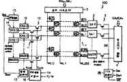
제 1 도는 본 발명의 제 1 실시예에 의한 반도체 메모리 장치의 개통도이다.1 is an opening diagram of a semiconductor memory device according to the first embodiment of the present invention.
제 1 도의 반도체 메모리 장치는 매트릭스형으로 배열된 다수의 다이나믹 RAM(D-RAM)셀들(MC)1과, 로우 어드레스신호들 RA0내지 RA7에 반응하여 메모리 셀들의 워드라인들 WL0내지 WL255를 선택하기 위한 로우 디코오더 5와, 비트라인들 BL0내지BL255및

제 1 도의 반도체 메모리 장치는 256개의 전송 게이트들을 포함하는 제 1 전송게이트 어레이 10들 통하여 비트라인들 BLo내지 BL255에 열결되는 직렬로 열결된 256개의 쉬프트 레지스터들 SRAo내지 SRA255를포함하는 데이타 판독 쉬프트 레지스터 어레이 12와 256개의 전송 게이트들을 포함하는 제 2 전송게이트 어레이 11을 통하여 비트라인들 BLo내지 BL255에 열결되는 직렬로 열결된 256개의 쉬프트 레지스터들 SRBo내지 SBR255를 갖는 데이타 기입 쉬프트 레지스터 어레이 14를 더 갖고 있다. 출력증폭기 13은 판독 쉬프트 레지스터 어레이 12에 열결된다.The semiconductor memory device of FIG. 1 includes 256 shift registers SRAo through SRA255 connected in series to bit lines BLo through BL255 through first
출력증폭기 13으로부터의 출력신호 SOUT는 도시안된 중앙처리유니트(CPU)로부터 변형회로 15로 변형 입력신호 SIN과 함께 공급된다 변형회로 15로부터의 출력신호는 기입 쉬프트 레지스터 어레이 14에 공급된다.The output signal SOUT from the
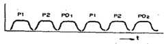
제 1 도의 판독 및 기입 쉬프트 레지스터들 SRAo내지 SRA255와 SRBo내지 SRB255의 전형적인 예는 제 2 도에 보인 바와 같이 2상 비율형(two-phase ratio type) 쉬프트 레지스터이다. 2상 비율형 쉬프트 레지스터의 타이밍 도포는 제 3 도에 나타나 있다. 쉬프트 레지스터 SR2는 전단의 쉬프트 레지스터 SR2의 노드 N14의 값이 마스터 데이타로서 전송되며, 트랜지스터 Q22는 노드 N21내의 마스트 데이타를 수신하도록 클록펄스 P1에 반응하여 턴온된다. 노드 N21의 전압 레벨이 논리"1"에 세트되면 노드 N22의 레벨은 반전된다. 후속되는 전송을 수행하기 위해 트랜지스터 Q26은 노드 N23의 레벨이 노드 N22의 레벨과 동일하게 세트되도록 클록펄스 P2에 반응하여 턴온된다. 노드 N2의 신호레벨온 노드 N23의 신호레벨에 의해 반전된다. 그러므로, 데이타는 각 쉬프트 레지스터내에서 한 비트씩 쉬프트 될 수 있다. 제 1 도의 반도체 메모리장치의 동작은 후술될 것이다. D-RAM측은 쉬프트 레지스터측과 비동기되어 그와 무관하게 동작된다. D-RAM은 종래의 방식으로 억세스될 수 있다. 그와 동시에 D-RAM이 비억세스모드에 유지되면 RMW동작은 다음식으로 수행될 수 있다.A typical example of the read and write shift registers SRAo through SRA255 and SRBo through SRB255 of FIG. 1 is a two-phase ratio type shift register as shown in FIG. The timing application of the two phase ratio type shift register is shown in FIG. The shift register SR2 is the value of the node N14 of the front end of the shift register SR2 as a master data transmission, the transistor Q22 is turned on in response to the clock pulse P1 to receive a mast data in the node N21. When the voltage level of node N21 is set to logic "1", the level of node N22 is inverted. Transistor Q26 is turned on in response to clock pulse P2 so that the level at node N23 is set equal to the level at node N22 to perform subsequent transfers. Signal level on node N2 is inverted by the signal level of node N23 . Therefore, data can be shifted by one bit in each shift register. The operation of the semiconductor memory device of FIG. 1 will be described later. The D-RAM side is asynchronous with the shift register side and operates independently of it. The D-RAM can be accessed in a conventional manner. At the same time, if the D-RAM remains in the non-access mode, the RMW operation can be performed in the following manner.
RMW 모드에서, 전송병렬 TR 및 판독병렬 R/W=O는 전숑 클륵구동기 16에 공급되며, 또한 구동기 16은 클록신호들 TCLKA를 발생시킨다. 전송게이트 어레이 10은 클륵신호 TCLKA에 반응하여 턴온되므로 억세스된 워드라연 WL1에 열결되는 비트라인들 BLO내지 BL255상의 데이타는 판독 쉬프트 레지스터 어레이 12에 동시에 공급된다.그 다음 쉬프트 레지스터 12내의데이타는 출력 증폭기 13에 의해 출력신호 SOUT로서연속적으로 판독되여 그 판독된 신호 SOUT를 변형회로 15로 공급해 준다.In the RMW mode, the transmit parallel TR and the read parallel R / W = O are supplied to the
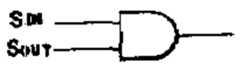
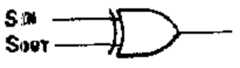
제 4 도에 보인 바와 같이 변형회로 15는 입력 신호IN을 중폭시키기 위한 증폭기 151과, 신호들 SIN및SOUT의 논리 OR를 발생시키기 위한 OR게이트 152 그리고 OR게이트 152로부터의 출력을 증폭시키기 위판중폭기 153을 포함한다. 신호 SOUT와 같은 초기신호는 제 4 도의 회로의 입력신호 SIN과 함께 논리적 으로 OR 열산된다. 그러나, 데이타 변형은 논리합(OR)으로 제한되지 않고, 논리급(제 5a도), 논리 익스클루시브 OR (제5b도) 또는 단순한 반전(제5c도)등으로 할 수 있다.As shown in FIG. 4, the
변형된 신호는 기입 쉬프트 레지스터 어레이 14내에 기억된다. 변형된 신호를이 쉬프트 레지스터들에 모두 로드될때 전송병렬 TR과 기입병렬 R/W=1이 전송 클럭 구동기 16에 공급된다. 게이트 어레이 11온 구동기 16으로부터 클록신호 TCLKB에 반응하여 턴온된다. 쉬프트 레지스터 어레이 14 내의 내용물은 상술힌워드 라인 WL1열결된 메모리 셀들내에 기억된다.The modified signal is stored in the write
이 경우에 메모리 셀들내의 데이타가 디스플레이 전용으로 사용될 때 쉬프트 레지스터 어레이 14의 최종단 SRB255에 열결되는 출력 증폭기(도시안됨)는 게이트 어레이 11이 오프 상태를 유지하는 동열 디스플레이상에 데이타를 출력하여 디스플레이 한다.In this case, an output amplifier (not shown) connected to the final stage SRB255 of the
상술한 바와 같이, 소정의 워드라연에 열결된 메모리 셀들들에 대해 고속 RMW 동작을 동시에 수행할 수있다.As described above, a high speed RMW operation may be simultaneously performed on memory cells connected to a predetermined word line.
상술한 실시예에서는 두재의 쉬프트 레지스터 어레이들이 RMW 동작들 위해 사용된다. 그러나 RMW동작은 단일 쉬프트 레지스터 어레이에 의해 수행될 수도 있다. 이 경우에, 한 쉬프트 레지스터 어레이는기입/판독 억세스를 수행하도록 단일 전송게이트 어레이를 통하여 워드라연에 열결된다.In the embodiment described above, two shift register arrays are used for RMW operations. However, the RMW operation may be performed by a single shift register array. In this case, one shift register array is concatenated to the word string through a single transfer gate array to perform write / read access.
상술한 반도체 메모리 장치는 모든 쉬프트 레지스터들에 대해 RMW 동작을 행한다. 그러나 일반적으로 RMW는 소정의 비트라인에 대해 수행된다. 이 응용에 직합판 실시예를 이후 설명한다 .The semiconductor memory device described above performs an RMW operation on all the shift registers. In general, however, RMW is performed for a given bitline. The embodiment of the non-woven board for this application will be described later.
제 6 도는 본 발명의 제 2 실시예에 의단 반도체 메모리 장치의 회로 배열을 나타낸다. 표시번호 100은 컬럼들의 유니트들내의 비트라인들과 각 부품들간의 열결들을 개략적으로 나타내도록 메모리 셀 어레이 1, 감지증폭기 어레이 2, 게이트 어레이 3. 컬럼 디코오더 4, 로우 디코오더 5 그러고 I/O 증폭기 25를 포함하는D-RAM장치(제1도)에 대응하는 회로를 나타낸다.6 shows a circuit arrangement of the semiconductor memory device according to the second embodiment of the present invention.
쉬프트 레지스터 어레이 21a는 256개의 전송 게이트들을 포함하는 전송 게이트 어레이 20a를 통하여 비트라인들 BLO, 내지 BL255에 열결된다. 쉬프트 레지스터 어레이 21a의 출력단자들은 256개의 게이트들 즉, 트랜지스터들을 포함하는 출력 게이트 어레이의 대응하는 입력단자들에 열결된다. 출력 게이트 어레이 22a의 트랜지스터들의 드레인들은 데이타 버스 DB에 열결된다. 데이타 버스 DB는 변형회로 25a에 열결된다.포인터 쉬프트 레지스터(PSR)어레이 23a는 출력 게이트 어레이 22a의 각 게이트들을 제어하도록 배열된다. 컬럼 디코오더 24a는 포인터 쉬프트 레지스터 어레이 23a내에 값들 로드시키도록 배열된다.The
쉬프트 레지스터 어레이 21a내의 각 쉬프트 레지스터는 제 2 도에 보인 것과 동일할 수도 있다. 쉬프트레지스터들 SR1및 SR2, 출력 게이트 22a와 RSR1및 RSR2간의 열결들을 재현한 한 회로 배열이 제 7 도에 보이고 있다. 제 7 도의 회로배열의 타이밍 챠트는 제 8 도에 보이고 있다. 데이타는 제 1 시예에서와 동일한 방식으로 클록신호들 P1과 P2에 반응하여 한 비트씩 쉬프트된다.그밖에 제 2 실시에에 의하면, 쉬프트 레지스터들내의 내용들은 포인터 쉬프트 레지스터 어레이 23a로부터 포인터 병렬신호 PO, 에 반응하여 데이타 버스들 SDB와
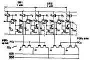
제 9 도는 포인터 숴프트 레지스터 어레이 23a의 일부의 회로도이다. n번째 포인터 쉬프트 레지스터PSRn은 공핍형 트랜지지스터 Q56과 고양형 트랜지스터 Q57및 Q60내지 Q65로 구성된다. 다른 포인터 쉬프트 레지스터들도 동일방식으로 구성된다. 제 10도는 포인터 쉬프트 레지스터 어레이 23a를 구동시키기 위한클록신호 TCLK1의 파형도이다. 포인터 쉬프트 레지스터들을 구동시키기 의한 제 10 도에 보인 클록펄스신호TCLK1은 서로간에 180도 위상 쉬프트된 제 1 펄스 PE와 제 2 펄스 NPE를 포함한다.9 is a circuit diagram of a portion of the pointer shaft register array 23a. n-th pointer shift register PSRn is composed of a depletion type transfected support requester Q56 and Enhancement type transistors Q57 and Q60 to Q65. The other pointer shift registers are configured in the same way. 10 is a waveform diagram of the clock signal TCLK1 for driving the pointer shift register array 23a. The clock pulse signal TCLK1 shown in FIG. 10 by driving the pointer shift registers includes a first pulse PE and a second pulse NPE that are phase shifted 180 degrees from each other.
포인터 쉬프트 레지스터들의 동작에 대해 이제 설명한다. 우선 펄스 PE가 고레벨에 있들때 (n-1)변예포인터 쉬프트 레지스터 PSRn-1의 출력 SLn-1은 고레벨 또는 논리 "1"이고, 모든 다른 출력들 SLo내지SLn-2와 SLn내지 SL255는 저레벨 또는 논리 "0"이라고 가정한다. 출력 SLn-1의 고레벨 전압공급으로 인해n번째 포인터 쉬프트 레지스터 PSRn내의트랜지스터 Q64는 턴온되어 결국, 노드 SPn이 고레벨로 충전된다. 노드 SPn과 SPn-1의 상태들은 펄스 PE가 저가될때 그대로 유지된다. 펄스 NPE가 고가 될때 트랜지스터들 Q62와 Q72는 턴온되어 노드 SPn의 고레벨신호를 트랜지스터 Q60의 게이트에 그리고 노드 SPn-1의 저레벨신호를 트랜지스터 Q70의 게이트에 공급한다. 트랜지스터들 Q60과 Q70의 각 게이트들에 공급된 신호들은 펄스 NPE가 저레벨이 되면 그대로 유지된다. 다시, 포인터 쉬프트 레지스터들 PSRn및 PSRn-1, 에 고레벨의 펄스 PE를 공급하여주면 노드들 SLn과 SLn-1의 신호 레벨들은 각각 고 및 저가 되므로, 결과적으로 유일한 "1"비트 데이타가 포인터 쉬프트 레지스터 PSRn-1로부터 인접 포인터 쉬프트 레지스터 PSRn으로 전송된다.The operation of the pointer shift registers is now described. First, when the pulse PE is itdeul a high level (n-1) byeonye pointer shift register output SLn-1 of the PSRn-1 is a high level or logic "1", all other outputs SLo to SLn-2, and SLn It is assumed that SL255 is a low level or logic "0". Due to the high level voltage supply of the output SLn-1 , transistor Q64 in the nth pointer shift register PSRn is turned on and eventually node SPn is charged to high level. The states of nodes SPn and SPn-1 remain unchanged when the pulse PE becomes low. When the pulse NPE goes high, transistors Q62 and Q72 are turned on to supply the high level signal of node SPn to the gate of transistor Q60 and the low level signal of node SPn-1 to the gate of transistor Q70 . The signals supplied to the respective gates of transistors Q60 and Q70 remain intact when pulse NPE goes low. Again, supplying the high level pulse PE to the pointer shift registers PSRn and PSRn-1 , the signal levels of the nodes SLn and SLn-1 are high and low, respectively, resulting in unique "1" bit data. Is transferred from the pointer shift register PSRn-1 to the adjacent pointer shift register PSRn .
트랜지스터 Q73A와 Q738는 노드 SLn-1을 저레벨로 안정되게 유지시키도록 트랜지스터 Q70의 게이트에 고전압이 공급되지 않도록 해준다. 트랜지스터 Q60의 게이트가 충분히 고전압을 공급받으면 트랜지스터 Q738의 게이트 전압은 노드 SLn이 고레벨로 변동됨과 동시에 신속히 저레벨로 된다.Transistors Q73A and Q738 ensure that no high voltage is applied to the gate of transistor Q70 to keep node SLn-1 low and stable. When the gate of transistor Q60 is supplied with a sufficiently high voltage, the gate voltage of transistor Q738 quickly goes to a low level while the node SLn is changed to a high level.
포인터 쉬프트 레지스터 PSRn내의트랜지스터들 Q56, Q57및Q61과 트랜지스터들 Q58, Q67및 Q71은 부유신호 레벨 즉, 저레벨로 인해 발생될 수도 있는 오동작을 방지하기 위해 사용된다. 왜냐하면 많은 노드들SL이 저레벨에 있기때문이다. 공핍 트랜지터들 Q56과 Q66은 저항들로 대치될 수도 있다.Transistors Q56 , Q57 and Q61 and transistors Q58 , Q67 and Q71 in pointer shift register PSRn are used to prevent malfunctions that may be caused by the stray signal level, ie low level. Because many nodes SL are at the low level. Depletion transistors Q56 and Q66 may be replaced with resistors.
포인터 쉬프트 레지스터 어레이 23a에 펄스들 PE 및 NPE의 쌍으로 구성되는 한 클록신호 TCLK1,을 공급항으로써 한 포인터 쉬프트 레지스터내에 유지되는 1비트 데이타는 그 다음 포인터 쉬프트 레지스터로 전송되고 한 포인터 쉬프트 레지스터는 리세트된다. 이것은 클록신호 TCLK1의 입력에 반응하여 연속적으로 실행된다. 포인터 쉬프트 레지스터 PSR0내지 PSR255는 그 내에서 유잉의 "1"비트 쉬프트하는 것이 특색이다.By supplying a clock signal TCLK1 , which is composed of a pair of pulses PE and NPE, to the pointer shift register array 23a, one bit of data held in one pointer shift register is then transferred to the pointer shift register and one pointer shift register is Reset. This is executed continuously in response to the input of the clock signal TCLK1 . The pointer shift registers PSR0 to PSR255 are characterized by Ewing's "1" bit shifting therein.
본 실시예에서는 제1비트라인 BL0와 n번째 비트라인 BLn-1간의 비트라인들상에 나타나는 임의의 수의일련의 데이타가 쉬프트 레지스터듣 SR0내지 SRn-1과 게이트 22a를 통하여 연속적으로 출력될 수 있으며.그 중 하나가 포인터 쉬프트 레지스터 어레이 23a 내에서 유일의"1"비트 쉬프트에 반응하여 선택된다. 출력데이타는 선택된 게이트 22a를 통하여 데이타 버스 DB상에 연속적으로 나타나며, 이는 출력중폭기(도시안됨)를 통하여 장치의 의부로 출력되어 결국 디스플레이 유니트에 대한 일면의 데이타가 얻어질 수 있다.In this embodiment, any number of series of data appearing on the bit lines between the first bit line BL0 and the nth bit line BLn-1 is continuously transmitted through the shift registers SR0 to SRn-1 and the
그렇지않으면, n번째 포인터 레지스터 PSRn-1은 논리 "1"에 세트되어 쉬프트 레지스터 어레이 21a의 소망하는 수의 쉬프트가 행해지는 동안 그에 계속 유지될 수도 있다. 이 동작온 또한 데이타 버스 DB를 통하여 소망하는 비트수의 일련의 데이타 출력들 유도해준다. 그러나, 데이타 쉬프트와 반대방향으로 유도해준다.Otherwise, the nth pointer register PSRn-1 may be set to a logic " 1 " and remain there for the desired number of shifts of the
변형회로 25a는 제1실시예의 것과 동일하다.제 6 도의 제 2 실시예에 의한 반도체 메모리창치의 RMW동작에 대해 이후 설명한다.The modified
전송병렬 TR이 논리 "1"에 세트되면 게이트 어레이 20a는 전송 클럭 구동기 26a로부터 클록실호 TCLK에반응하여 턴온되므로 결국 데이타는 예정된 워드라인과 비트라인들 BLo내지 BL255에 의해 정해진 256개의메모리 셀들로부터 레지스터 어레이 21a로 동시에 전송된다.When the transmit-parallel TR is set to a logic "1", the gate array 20a is turned on in response to the clock signal TCLK from the transmit
RMW 동작에 대한 하나의 양호한 모드에 의하면 포인터 쉬프트 레지스터들 PSRo내지 PSR255중 임의의 것으로부터의 출력은 논리 "1"에 세트되며, 그리고 레지스터 어레이 21a의"1"을 보지하고 있는 쉬프트 레지스터에 열결된 출력 게이트는 턴온되는 한편, 쉬프트 레지스터들 SR0내지 SRn-1의 데이타는 클륵 펄스(도시안됨)에 반응하여 1비트만큼 쉬프트된다. 그와 동시에 쉬프트 레지스더 SRn-1로부터의 출력은 데이타 버스들 SDB와
상술한 바와 동일한변형 동작이 n비트들에 대해서도 수행된다.The same modification operation as described above is performed for n bits.
RMW 동작의 다른 모드에 의하면, 포인터 쉬프트 레지스터들 PSRo내지 PSR255중 하나는 논리"1"에 세트되고 그리고 쉬프트 레지스더 어레이들 21a와 23a는 동시에 쉬프트 된다. 이 동작을 행하는 동안 n 쉬프트 레지스터를 SR0내지 SRn-1은 쉬프트수에 대응하는 수 n과 함께 입력신호 SIN에 의해 하나의 포인터레지스터에 의해 최초로 억세스된 데이타를 변형시킨 결과와 동일한데이타를 기억시킨다.According to another mode of RMW operation, one of the pointer shift registers PSRo through PSR255 is set to a logic " 1 " and the
변형된 내용들은 그의 내용을 갱신하도록 메모리 셀들내에 재기억될 필요가 없으나, 쉬프트 레지스터 어레이 21a로부터 다른 장치로 공급될 수 있다.The modified contents do not need to be re-memorized in the memory cells to update their contents, but can be supplied from the
상술한 설명으로 부터 명백한 바와같이 고속 RMW 동작은 소정법위의 제 1 번째 내지 n번째 비트라인들BLo내지 BLn-1에 대해 수행될 수 있으며, 또한 로우 디코오더는 소정범위의 워드라인들내의 RMW 동작을 수행하도록 제어될 수 있다.As is apparent from the above description, the fast RMW operation may be performed on the first through nth bit lines BLo through BLn-1 of the predetermined method, and the low decoder may be performed within the range of word lines. It may be controlled to perform an RMW operation.
상기 실시예에서 제1번째 내지 n번째 비트라인들상의 데이타가 변형된다. 그러나, n1내지 n2번째 비트라인들의 변형 범위가 선택될 수 있다.In this embodiment, the data on the first to nth bit lines is transformed. However, a deformation range of n1 to n2 bit lines may be selected.
본 발명의 또다른 실시예가 제11도에 도시 되어있다. 제11도의 회로에서, 제 6 도의 쉬프트 레지스터 어레이 21a는 세트-리세트(R-S) 플립플롭 어레이로 대치된다. 보다 구체적으로 쉬프트 레지스터 대신에 플립플롭 273, 오아게이트 271, 그리고 인버어터 272로 구성되는 래치회로 27b가 래치회로 27b와 연관된 게이트들 22b와 28b와 함께 사용된다. 동작중, 비트라인 BL1상의 메모리셀들의 내용들은 판독되어 게이트 20a와 오아게이트 271들 통하여 플립플롭 273내에 기억된다. 프립플롭 273의 출력 Q는 포인터 쉬프트 레지스터 PSR1로부터 게이트 22a를 통해 데이타버스 DB로 포인터 병렬 PO1거에 의해 추출된다. 데이타베이스 DB상의 데이타는 변형회로 25a에 의해 변형된다. 변형된 내용은 게이트 22b와 오아게이트 271을 통해 플립플롭 273내에 기억된다. 변형 기억된 내용의 출력 Q는 클륵신호 TCLKB에 반응하여 게이트 28b를 통하여 비트라인 BL1에 연결된 메모리 셀내에 기억된다.Another embodiment of the invention is shown in FIG. In the circuit of FIG. 11, the
RMW 동작시간을 증가시키기 위해 n개의 병렬 RMW 회로배열이 제12도에 나타나 있다. 제12도의 희로와 메모리셀 어레이 100간의 열결은 상술한 것과 동일하다.그러나 n개의 병렬 RMW 동작을 수행하기 위해 n개의 데이타 버스들 DB-1 내지 DB-n과 n개의 변형회로(MDY) 25-1 내지 25-n이 배열된다. 더우기 n개의 포인터 레지스터 어레이들 23-1 내지 23-n은 n개의 레지스터 어레이 21-1 내지 21-n과 병렬로 동작될 수 있다. 포인터 레지스터 어레이들 23-1 내지 23-n과 레지스터 어레이들 21-1 내지 21-n은쉬프트 레지스터들이나 플립플롭일 수도 있다. 변형회로들 25-1 내지 25-n은 변형회로 25와 동일하다. 변형회로는 제 4 도 및 5a 내지 5c도 또는 다른 도면에 보인 바와같이 회로를 포함할 수도 있다. 제 4 및 5a내지 5c도에 보인 회로들은 각종 RMW 동작들을 수행하기 위해 선택적으로 사용될 수 있다.N parallel RMW circuit arrangements are shown in FIG. 12 to increase the RMW operating time. The thermal connection between the furnace of FIG. 12 and the
특정한 영역의 메모리셀들 (m×n)에 대해 RM`V 동작을 수행하기 위한 실시예들은 제13 및 14도에 각각 도시되어 있다.Embodiments for performing the RM'V operation on the memory cells m × n in a specific region are shown in FIGS. 13 and 14, respectively.
제13도의 회로는 비트라인들 BL1내지 BL511중 대응하는 것에 열결되는 일단을 각각 갖는 게이트들 Q0내지 Q511로 구성되는 게이트 어레이 31과, 대응하는 게이트들 Q0내지 Q511의 타단에 열결되는 일단을 각각 갖는 데이타 랫치들 DL0내지 DL511로 구성되는 랫치 어레이 32와, 대응하는 데이타 랫치들 DL0내지DL511의 타단에 각각 열결되는 게이트들 QAO내지 Q511로 구성되는 게이트 어레이 33과, 게이트 어레이33의 게이트들을 제어하기 위한 쉬프트 레지스터들 SRO내지 SR511로 구성되는 쉬프트 레지스터 어레이 34를 갖고 있다. 게이트 어레이 33은 변형회로 25a가 열결외는 데이타버스 DB에 열결된다. 본 실시예에서, 메모리 셀 어레이는 512×512 매트릭스를 가지며, 또한 다른 회로 배열들은 종전회로의 것들과 동일하다.The circuit of FIG. 13 has a
제13도에 보인 회로의 동작에 대해 이하 설명한다. 메모리 셀측이 억세스되지 않으면 로우 디코오더 5에의해 특정한 워드라인 WLj가 선택된다. 클록신호 ψS가 이네이블(고)이면 게이트 어레이 34의 모든 게이트들 Q0내지 Q511이 턴온되므로 결국 워드라인 WLj에 열결된 메모리 셀들의 내용들은 비트라인들 BLo내지BL511과 게이트들 Qo내지 Q511을 통하여 데이타 랫치들 DL0내지 DL511로 전송된다. 클록신호 ψS는 상술한 데이타 전송기간후 디스이네이블된다. 그후 메모리셀들은 억세스될 수 있다.The operation of the circuit shown in FIG. 13 will be described below. If the memory cell side is not accessed, a specific word line WLj is selected by row decoder 5. If the clock signal ψS is enabled (high), all the gates Q0 through Q511 of the
데이타 랫치들 DL0내지 DL511에 의해 랫치된 내용들 가운데, 쉬프트 레지스터 어레이 34, 예, SR1내지 SRi+n에 대한 특정 레지스터들의 내용들은 RMW 동작에 지배된다. 쉬프트 레지스터들 SR0내지 SRi-1은컬럼 디코오더 24a로 부터의 신호들 CL0내지 CLi-1에 반응하여 오프로 유지되므로, 쉬프트 레지스터들SRo내지 SRi-1로부터의 출력들은 오프로 유지된다. 그러므로, 게이트들 QAO내지 QA(i-1)은 오프로 유지되어 데이타 랫치들 DLo내지 DLi-1의 내용들은 바뀌지 않고, 그대로 있는다. 쉬프트 레지스터들 SRi내지SR1+n은 컬럼 디코오더 24a로 부터 신호들 CL 내지 CL1+n에 반응하여 순서적으로 턴온된다. 게이트 QA1내지 QA(i+n)은 온출력들 CLi내지 CLi+n에 반응하여 순서적으로 턴온된다. 이 경우에 입력 데이타 Din은데이타버스 DB에 공급되며 또한, 변형회로 25a에 의해 변형된 내용들은 데이타 랫치들 DLi내지 Di+n에의해 순서적으로 랫치된다. 데이타 랫치들 DLi+n+1내지 DL511과 DLo내지 DLi-1은 변형없이 메모리 셀들의 내용들을 기억시킨다. 워드라인 WL1에 대한 비트라인들 Bj내지 BLi+n의 범위내에서 변형된 내용들은데이타 랫치들 DLi내지 DLi+n내에 유지되는 한편 기타 랫치들은 변형없이 메모리 셀들의 내용들을 기억시킨다.Among the contents latched by the data latches DL0 through DL511 , the contents of the specific registers for the
이 상태에서, 클록신호 ψS는 메모리 셀들이 억세스되지 않는 소정기간동안 이네이블된다. 게이트어레이31은 턴온되어 데이타 랫치 어레이 32의 내용들은 워드라연 WLj에 열결되는 메모리 셀들내에 기억된다. 변형된 내용들은 비트라인들 BLi, 내지 BLi+n의 법위내의메모리 셀들내에 기억될 수 있다. 다른 메모리 셀들은 종전 데이타를 유지한다. 동일한동작이 워드라인들 WLj+1내지 WLj+m에 대해 수행되므로, 고속 RMW 동작이 특정 메모리 셀영역(m×n)에 대해 수행될 수 있다. 제14도는 제13도의 게이트 어레이 33이 입력 데이타버스 DB(I)에 열결되는 게이트들 QBO내지 QB511을구성하는 게이트 어레이 35와 출력 데이타버스 DB(O)에 열결되는 게이트를 QAO내지 QA511로 구성되는 게이트 어레이 33을 포함하고 있는 변형예를 보여주고 있다.In this state, the clock signal ψS is enabled for a predetermined period of time during which the memory cells are not accessed.
데이타 랫치들 DLo내지 DL511에 임시로 전송되는 메모리 셀들의 내용들은 i 내지 i+n의 특정범위내에서 입력데이타 Din과 함께 변형회로 25a에 의해 변형되며 또한 변형된 내용들은 데이타 랫치들 D10내지DL511에 의해 랫치된다. 변형된 내용들은 상술한 바와 동일한 방식으로 메모리 셀 어레이의 비억세스 모드동안 메모리 셀들내에 기억될 수 있다.The contents of the memory cells temporarily transmitted to the data latches DLo through DL511 are modified by the
이 회로에서, 고속 RMW 동작이 특정 메모리 셀 어레이(m×n)에 대한 메모리 내용들에 대해 수행될 수있으며, 또한 다른 메모리 셀 영역의 내용들은 변정되지 않고 그대로 남아있는다.In this circuit, a fast RMW operation can be performed on the memory contents for a particular memory cell array m × n, and the contents of the other memory cell region remain unchanged.
본 발명의 수많은 다른 실시예들을 본 발명의 정신과 정구범위에서 벗어나지 않는 범위내에서 실시 가능하다는 것을 본 분야에 속면된자들은 이해할 것이다.It will be understood by those skilled in the art that numerous other embodiments of the invention may be practiced without departing from the spirit and scope of the invention.
Claims (11)
Translated fromKoreanApplications Claiming Priority (3)
| Application Number | Priority Date | Filing Date | Title |
|---|---|---|---|
| JP59221165AJPS61104391A (en) | 1984-10-23 | 1984-10-23 | semiconductor storage device |
| JP221165 | 1984-10-23 | ||
| JP59-221165 | 1984-10-23 |
Publications (2)
| Publication Number | Publication Date |
|---|---|
| KR860003611A KR860003611A (en) | 1986-05-28 |
| KR900007226B1true KR900007226B1 (en) | 1990-10-05 |
Family
ID=16762485
Family Applications (1)
| Application Number | Title | Priority Date | Filing Date |
|---|---|---|---|
| KR1019850007804AExpiredKR900007226B1 (en) | 1984-10-23 | 1985-10-23 | Semiconductor memory device |
Country Status (5)
| Country | Link |
|---|---|
| US (1) | US4740922A (en) |
| EP (1) | EP0188059B1 (en) |
| JP (1) | JPS61104391A (en) |
| KR (1) | KR900007226B1 (en) |
| DE (1) | DE3585733D1 (en) |
Families Citing this family (26)
| Publication number | Priority date | Publication date | Assignee | Title |
|---|---|---|---|---|
| US5270981A (en)* | 1985-07-30 | 1993-12-14 | Kabushiki Kaisha Toshiba | Field memory device functioning as a variable stage shift register with gated feedback from its output to its input |
| JPS6243744A (en)* | 1985-08-21 | 1987-02-25 | Nec Corp | Microcomputer |
| JPS6314395A (en)* | 1986-07-04 | 1988-01-21 | Nec Corp | Storage circuit |
| GB8616852D0 (en)* | 1986-07-10 | 1986-08-20 | Hughes Microelectronics Ltd | Electronic counter |
| US4891752A (en)* | 1987-03-03 | 1990-01-02 | Tandon Corporation | Multimode expanded memory space addressing system using independently generated DMA channel selection and DMA page address signals |
| US4849875A (en)* | 1987-03-03 | 1989-07-18 | Tandon Corporation | Computer address modification system with optional DMA paging |
| KR960005392B1 (en)* | 1987-08-10 | 1996-04-24 | 탄돈 코포레이션 | Computer system for providing address modification for use also with dma and interrupt |
| US5101339A (en)* | 1987-08-10 | 1992-03-31 | Tandon Corporation | Computer address modification system using writable mapping and page stores |
| DE3733012A1 (en)* | 1987-09-30 | 1989-04-13 | Thomson Brandt Gmbh | STORAGE ARRANGEMENT |
| JP2542248B2 (en)* | 1988-11-17 | 1996-10-09 | 三菱電機株式会社 | Semiconductor memory device |
| US4980828A (en)* | 1988-11-25 | 1990-12-25 | Picker International, Inc. | Medical imaging system including use of DMA control for selective bit mapping of DRAM and VRAM memories |
| AU645251B2 (en)* | 1989-05-08 | 1994-01-13 | United Module Corporation | Real-time adjustable-transform device driver |
| US5214761A (en)* | 1989-05-08 | 1993-05-25 | Wang Laboratories, Inc. | Real-time adjustable-transform device driver for physical devices |
| US5167029A (en)* | 1989-12-13 | 1992-11-24 | International Business Machines Corporation | Data processing system and associated process using memory cards having data modify functions utilizing a data mask and an internal register |
| EP0446847B1 (en)* | 1990-03-12 | 1998-06-17 | Nec Corporation | Semiconductor memory device having improved write function |
| JP2604276B2 (en)* | 1990-11-20 | 1997-04-30 | 三菱電機株式会社 | Semiconductor storage device |
| US5270970A (en)* | 1991-03-15 | 1993-12-14 | Motorola, Inc. | Memory device having a buffer for gating data transmissions |
| DE4228213C2 (en)* | 1991-09-19 | 1997-05-15 | Siemens Ag | Integrated semiconductor memory circuit and method for its operation |
| JPH06111010A (en)* | 1992-09-29 | 1994-04-22 | Ricoh Co Ltd | DRAM and controller |
| WO1995010804A1 (en)* | 1993-10-12 | 1995-04-20 | Wang Laboratories, Inc. | Hardware assisted modify count instruction |
| US5802586A (en)* | 1995-02-27 | 1998-09-01 | Motorola, Inc. | Cache memory having a read-modify-write operation and simultaneous burst read and write operations and a method therefor |
| US6804162B1 (en)* | 2001-04-05 | 2004-10-12 | T-Ram, Inc. | Read-modify-write memory using read-or-write banks |
| DE10340861A1 (en)* | 2003-09-04 | 2005-04-07 | Infineon Technologies Ag | A processor circuit and method for associating a logic chip with a memory chip |
| US7212431B2 (en)* | 2004-12-29 | 2007-05-01 | Hynix Semiconductor Inc. | Nonvolatile ferroelectric memory device and control method thereof |
| US9350386B2 (en) | 2012-04-12 | 2016-05-24 | Samsung Electronics Co., Ltd. | Memory device, memory system, and method of operating the same |
| KR20220106307A (en) | 2021-01-22 | 2022-07-29 | 삼성전자주식회사 | Storage device and method for operating the device |
Family Cites Families (10)
| Publication number | Priority date | Publication date | Assignee | Title |
|---|---|---|---|---|
| US3763480A (en)* | 1971-10-12 | 1973-10-02 | Rca Corp | Digital and analog data handling devices |
| US3757313A (en)* | 1972-06-29 | 1973-09-04 | Ibm | Data storage with predetermined settable configuration |
| US4272829A (en)* | 1977-12-29 | 1981-06-09 | Ncr Corporation | Reconfigurable register and logic circuitry device for selective connection to external buses |
| US4276609A (en)* | 1979-01-04 | 1981-06-30 | Ncr Corporation | CCD memory retrieval system |
| JPS6045499B2 (en)* | 1980-04-15 | 1985-10-09 | 富士通株式会社 | semiconductor storage device |
| JPS5727477A (en)* | 1980-07-23 | 1982-02-13 | Nec Corp | Memory circuit |
| JPS57117168A (en)* | 1981-01-08 | 1982-07-21 | Nec Corp | Memory circuit |
| US4412313A (en)* | 1981-01-19 | 1983-10-25 | Bell Telephone Laboratories, Incorporated | Random access memory system having high-speed serial data paths |
| US4422161A (en)* | 1981-10-08 | 1983-12-20 | Rca Corporation | Memory array with redundant elements |
| JPS60236184A (en)* | 1984-05-08 | 1985-11-22 | Nec Corp | Semiconductor memory |
- 1984
- 1984-10-23JPJP59221165Apatent/JPS61104391A/enactiveGranted
- 1985
- 1985-10-17USUS06/788,398patent/US4740922A/ennot_activeExpired - Fee Related
- 1985-10-22EPEP85307600Apatent/EP0188059B1/ennot_activeExpired - Lifetime
- 1985-10-22DEDE8585307600Tpatent/DE3585733D1/ennot_activeExpired - Lifetime
- 1985-10-23KRKR1019850007804Apatent/KR900007226B1/ennot_activeExpired
Also Published As
| Publication number | Publication date |
|---|---|
| US4740922A (en) | 1988-04-26 |
| JPH0542078B2 (en) | 1993-06-25 |
| DE3585733D1 (en) | 1992-04-30 |
| EP0188059A1 (en) | 1986-07-23 |
| JPS61104391A (en) | 1986-05-22 |
| EP0188059B1 (en) | 1992-03-25 |
| KR860003611A (en) | 1986-05-28 |
Similar Documents
| Publication | Publication Date | Title |
|---|---|---|
| KR900007226B1 (en) | Semiconductor memory device | |
| US4344156A (en) | High speed data transfer for a semiconductor memory | |
| US4633441A (en) | Dual port memory circuit | |
| US4685089A (en) | High speed, low-power nibble mode circuitry for dynamic memory | |
| DE3586523T2 (en) | SEMICONDUCTOR MEMORY ARRANGEMENT WITH A SERIAL DATA INPUT AND OUTPUT CIRCUIT. | |
| US4680738A (en) | Memory with sequential mode | |
| EP0360526A1 (en) | Semiconductor memory device having flash write function | |
| EP0364110B1 (en) | Semiconductor memory device having a serial access memory | |
| US5418750A (en) | Semiconductor memory device for suppressing noises occurring on bit and word lines | |
| JPS61160898A (en) | Semiconductor memory device | |
| US4669064A (en) | Semiconductor memory device with improved data write function | |
| US5493536A (en) | Dual-port random access memory having memory cell controlled by write data lines and read enable line | |
| US5379263A (en) | Semiconductor memory device which can provide required data flexibly under simplified control and operating method therefor | |
| US4395765A (en) | Multiport memory array | |
| US5381363A (en) | Method and circuitry for performing a hidden read-modify-write | |
| US5307323A (en) | Dual-port memory | |
| EP0534394A2 (en) | Semiconductor memory device and method for controlling its output | |
| EP0381940B1 (en) | Register bank circuit | |
| US5787311A (en) | Integrated circuit multiport memory having serial access bit mask register and method for writing in the multiport memory | |
| KR960700490A (en) | METHOD AND APPARATUS FOR PROVIDING OPERATIONS AFFECTING A FRAME BUFFER WITHOUT A ROW ADDERSS STROBE CYCLE | |
| US5654934A (en) | Semiconductor memory employing a block-write system | |
| JP3102754B2 (en) | Information utilization circuit | |
| JPH0778989B2 (en) | Semiconductor memory device | |
| KR100487005B1 (en) | High Speed Video Frame Buffer | |
| KR930000960B1 (en) | Semiconductor memory device |
Legal Events
| Date | Code | Title | Description |
|---|---|---|---|
| A201 | Request for examination | ||
| PA0109 | Patent application | St.27 status event code:A-0-1-A10-A12-nap-PA0109 | |
| PA0201 | Request for examination | St.27 status event code:A-1-2-D10-D11-exm-PA0201 | |
| R17-X000 | Change to representative recorded | St.27 status event code:A-3-3-R10-R17-oth-X000 | |
| PG1501 | Laying open of application | St.27 status event code:A-1-1-Q10-Q12-nap-PG1501 | |
| E902 | Notification of reason for refusal | ||
| PE0902 | Notice of grounds for rejection | St.27 status event code:A-1-2-D10-D21-exm-PE0902 | |
| T11-X000 | Administrative time limit extension requested | St.27 status event code:U-3-3-T10-T11-oth-X000 | |
| T11-X000 | Administrative time limit extension requested | St.27 status event code:U-3-3-T10-T11-oth-X000 | |
| T11-X000 | Administrative time limit extension requested | St.27 status event code:U-3-3-T10-T11-oth-X000 | |
| P11-X000 | Amendment of application requested | St.27 status event code:A-2-2-P10-P11-nap-X000 | |
| P13-X000 | Application amended | St.27 status event code:A-2-2-P10-P13-nap-X000 | |
| G160 | Decision to publish patent application | ||
| PG1605 | Publication of application before grant of patent | St.27 status event code:A-2-2-Q10-Q13-nap-PG1605 | |
| E701 | Decision to grant or registration of patent right | ||
| PE0701 | Decision of registration | St.27 status event code:A-1-2-D10-D22-exm-PE0701 | |
| GRNT | Written decision to grant | ||
| PR0701 | Registration of establishment | St.27 status event code:A-2-4-F10-F11-exm-PR0701 | |
| PR1002 | Payment of registration fee | St.27 status event code:A-2-2-U10-U11-oth-PR1002 Fee payment year number:1 | |
| PR1001 | Payment of annual fee | St.27 status event code:A-4-4-U10-U11-oth-PR1001 Fee payment year number:4 | |
| PR1001 | Payment of annual fee | St.27 status event code:A-4-4-U10-U11-oth-PR1001 Fee payment year number:5 | |
| PR1001 | Payment of annual fee | St.27 status event code:A-4-4-U10-U11-oth-PR1001 Fee payment year number:6 | |
| PR1001 | Payment of annual fee | St.27 status event code:A-4-4-U10-U11-oth-PR1001 Fee payment year number:7 | |
| FPAY | Annual fee payment | Payment date:19970830 Year of fee payment:8 | |
| PR1001 | Payment of annual fee | St.27 status event code:A-4-4-U10-U11-oth-PR1001 Fee payment year number:8 | |
| LAPS | Lapse due to unpaid annual fee | ||
| PC1903 | Unpaid annual fee | St.27 status event code:A-4-4-U10-U13-oth-PC1903 Not in force date:19981006 Payment event data comment text:Termination Category : DEFAULT_OF_REGISTRATION_FEE | |
| PN2301 | Change of applicant | St.27 status event code:A-5-5-R10-R13-asn-PN2301 St.27 status event code:A-5-5-R10-R11-asn-PN2301 | |
| PN2301 | Change of applicant | St.27 status event code:A-5-5-R10-R13-asn-PN2301 St.27 status event code:A-5-5-R10-R11-asn-PN2301 | |
| R18-X000 | Changes to party contact information recorded | St.27 status event code:A-5-5-R10-R18-oth-X000 | |
| R18-X000 | Changes to party contact information recorded | St.27 status event code:A-5-5-R10-R18-oth-X000 | |
| PC1903 | Unpaid annual fee | St.27 status event code:N-4-6-H10-H13-oth-PC1903 Ip right cessation event data comment text:Termination Category : DEFAULT_OF_REGISTRATION_FEE Not in force date:19981006 | |
| PN2301 | Change of applicant | St.27 status event code:A-5-5-R10-R13-asn-PN2301 St.27 status event code:A-5-5-R10-R11-asn-PN2301 | |
| P22-X000 | Classification modified | St.27 status event code:A-4-4-P10-P22-nap-X000 |