KR900004035B1 - Luminance and Color Signal Reduction Reduction Circuit in Color Television Receiver - Google Patents
Luminance and Color Signal Reduction Reduction Circuit in Color Television ReceiverDownload PDFInfo
- Publication number
- KR900004035B1 KR900004035B1KR1019860011759AKR860011759AKR900004035B1KR 900004035 B1KR900004035 B1KR 900004035B1KR 1019860011759 AKR1019860011759 AKR 1019860011759AKR 860011759 AKR860011759 AKR 860011759AKR 900004035 B1KR900004035 B1KR 900004035B1
- Authority
- KR
- South Korea
- Prior art keywords
- color
- signal
- output
- circuit
- luminance
- Prior art date
- Legal status (The legal status is an assumption and is not a legal conclusion. Google has not performed a legal analysis and makes no representation as to the accuracy of the status listed.)
- Expired
Links
Images


Classifications
- H—ELECTRICITY
- H04—ELECTRIC COMMUNICATION TECHNIQUE
- H04N—PICTORIAL COMMUNICATION, e.g. TELEVISION
- H04N5/00—Details of television systems
- H04N5/14—Picture signal circuitry for video frequency region
- H04N5/21—Circuitry for suppressing or minimising disturbance, e.g. moiré or halo
- H—ELECTRICITY
- H04—ELECTRIC COMMUNICATION TECHNIQUE
- H04N—PICTORIAL COMMUNICATION, e.g. TELEVISION
- H04N9/00—Details of colour television systems
- H04N9/77—Circuits for processing the brightness signal and the chrominance signal relative to each other, e.g. adjusting the phase of the brightness signal relative to the colour signal, correcting differential gain or differential phase
Landscapes
- Engineering & Computer Science (AREA)
- Multimedia (AREA)
- Signal Processing (AREA)
- Processing Of Color Television Signals (AREA)
Abstract
Translated fromKoreanDescription
Translated fromKorean제 1 도는 종래의 칼라텔레비죤 신호처리 회로 블럭도.1 is a block diagram of a conventional color television signal processing circuit.
제 2 도는 종래의 1H형 콤필터를 사용한 칼라텔레비죤 신호처리 회로 블럭도.2 is a block diagram of a color television signal processing circuit using a conventional 1H comb filter.
제 3 도는 종래의 2H형 콤필터를 사용한 칼라텔레비죤 신호 회로처리 블럭도.3 is a block diagram of a color television signal circuit using a conventional 2H comb filter.
제 4 도는 본 발명에 따른 칼라텔레비죤 신호처리 회로 블럭도.4 is a block diagram of a color television signal processing circuit according to the present invention.
제 5 도는 상기 제 4 도의 또 다른 실시예인 2H형 크로마 콤필터.5 is a 2H type chroma comb filter according to another embodiment of FIG.
제 6(a)(b) 도는 복합 영상신호에서의 칼라 부반송파 위상관계도.6 (a) (b) is a diagram of color subcarrier phase relationships in a composite video signal.
제 7 도는 제 4 도에 의한 휘도신호대역과 색신호대역의 주파수 선택특성도.7 is a frequency selective characteristic diagram of a luminance signal band and a color signal band according to FIG.
* 도면의 주요부분에 대한 부호의 설명* Explanation of symbols for main parts of the drawings
100 : 영상버퍼 200 : 지연회로100: video buffer 200: delay circuit
300 : 색부반송파 트랩회로 400 : 색신호 대역 통과필터300: color carrier carrier trap circuit 400: color signal band pass filter
500 : 1H 지연기 600 : 반전기500: 1H delayer 600: Inverter
700 : 가산기700: adder
본 발명은 칼라텔레비죤에 있어서, 휘도신호 및 색신호 방해 경감회로에 관한 것으로, 특히 색신호 통과대역필터 부분에 크로마 콤필터를 접속하여 복합영상 신호로부터 휘도신호와 색신호를 분리시 발생되는 크로스 칼라(Cros Color)방해와 수직방향으로 급격히 변화하는 신호에 의하여 휘도신호 대역에 발생되는 도트 방해신호를 제거하는 회로에 관한 것이다.BACKGROUND OF THE INVENTION 1. Field of the Invention The present invention relates to a luminance signal and a color signal disturbance reduction circuit in a color television. Particularly, a cross color generated when a luminance signal and a color signal are separated from a composite video signal by connecting a chroma comb filter to a color signal passband filter portion. The present invention relates to a circuit for removing a dot disturb signal generated in a luminance signal band by a signal rapidly changing in the vertical direction with interference.
통상적으로 텔레비죤의 휘도(Luminance)신호는 텔레비죤의 명암을 나타낸는 신호이며, 색신호(Chrominance Signal)은 칼라텔레비죤의 색정보로 변조된 색부반송파의 측파대를 말하는 것으로, NTSC방식의 경우 휘도신호의 위상은 매 수평라인마다 동일하며 색신호의 위상은 매 수평라인마다 반전되고 있다.In general, the luminance signal of the television is a signal representing the contrast of the television, and the chroma signal refers to the sideband of the color subcarrier modulated by the color information of the color television. Every horizontal line is the same, and the phase of the color signal is inverted every horizontal line.
상기 색신호는 휘도신호에 중첩되어 칼라 영상신호로 전송되며, 색신호의 진폭이 색의 채도를 나타내고 있으며 위상이 색상을 나타내고 있다. 이 색부반송파로 변조된 색신호 주파수 스펙트럼은 수평주사 주파수의 고주파 성분들과는 주파수 삽입(Interlace)의 관계가 있으며 NTSC방식에서는 3.579545MHZ이다.The color signal is superimposed on the luminance signal and transmitted as a color image signal, where the amplitude of the color signal represents color saturation and the phase represents color. The color signal frequency spectrum modulated by this color subcarrier has an interlace relationship with the high frequency components of the horizontal scanning frequency, and is 3.579545MHZ in the NTSC method.
상기 휘도신호와 색신호(반송 색신호)가 합쳐져 복합 영상신호를 구성하고 있다.The luminance signal and the color signal (transfer color signal) are combined to form a composite video signal.
이와같이 구성된 복합 영상신호로서 텔레비죤의 영상을 시청하기 위해서는 복합영상 신호로부터 휘도 및 색신호를 각각 분리하여 상기 휘도신호는 영상증폭회로로, 색신호는 ACC 및 색복조회로로 각각 인가되게하여 증폭 및 복조하여 신호를 처리함으로서 시청할 수 있게 된다.In order to view a television image as a composite video signal configured as described above, the luminance and color signals are separated from the composite video signal, and the luminance signals are applied to the image amplification circuit and the color signals are respectively amplified and demodulated. By processing, it becomes possible to watch.
종래의 칼라 텔레비죤(Color Television) 신호처리 회로 즉 휘도신호/색신호 분리회로는 제 1 도에 도시한 바와같이 복합 영상신호(Composite Video Signal)를 입력하여 완충하고 버퍼링하기 위한 영상버퍼(1)와, 상기 영상버퍼(1)에서 출력되는 복합 영상신호를 지연출력하는 지연회로(2)와, 상기 지연회로(2)를 통해 지연입력되는 복합 영상신호중에 포함된 3.579545MHz의 색부반송파(3.58MHz Dot 방해신호)를 제거하여 휘도신호(Y)만을 출력하기 위한 색부반송파 트랩회로(3)와, 상기 복합 영상신호를 입력하여 색신호 대역만을 통과시키어 ACC(Automatic Color Control)(도시하지 않음) 및 색복조회로로 출력하는 색신호 대역 통과필터(4)로 구성된다.A conventional color television signal processing circuit, that is, a luminance signal / color signal separation circuit, includes an image buffer 1 for inputting and buffering and buffering a composite video signal as shown in FIG. A
상기한 구성중 미설명 참조번호 102는 복합 영상신호(CVS)를 입력하는 복합 영상신호 입력단자이고, 104는 색부반송파 트랩회로(3)의 출력단자로서 상기 색부반송파 트랩회로(3)로부터 출력되는 휘도신호(Y)를 DC클램프회로(도시하지 않음)와 영상 증폭회로(도시하지 않음)에 입력시키도록 접속된 단자이다.In the above configuration,
그리고 참조번호 106은 색신호 대역 통과필터(4)의 출력단자로서 ACC 및 색복조회로에 접속되어 상기색신호 대역 통과필터(4)로부터 출력되는 변조된 색신호(C)를 출력하는 단자이다.
상기와 같이 구성된 회로는 이미 주지된 바와같이 휘도채널에 색부반송파 트랩회로(3), 색도채널에는 색신호 대역 통과필터(4)만을 설치 접속함으로서 휘도신호 대역에 발생되는 도트 방해신호를 제거할 수 있으나 휘도신호의 고역부분이 상실되어 해상도가 저하하게 되었으며, 색신호 대역 주파수 부근의 휘도신호가 색신호에 간섭을 주게 되어 크로스컬러(Cross Color)가 발생하는 문제가 있있다.The circuit configured as described above can eliminate the dot interference signal generated in the luminance signal band by installing and connecting the color
한편 상기 제 1 도와 같이 구성되었을때 발생되었던 문제를 해소코저 하여 1H형 콤필터(COMB FILTER)를 사용한 제 2 도 회로와, 2H형 콤필터(COMB FILTER)를 사용한 제 3 도의 회로가 있다.On the other hand, there is a circuit of FIG. 2 using a 1H type COMB FILTER and a circuit of FIG. 3 using a 2H type COMB FILTER to solve the problems caused when the first diagram is configured as described above.
제 2 도는 1H형 콤필터를 사용한 종래의 칼라TV 신호처리 블럭도로서, 단자(102)로 입력되는 복합 영상신호(CVS)를 1H(1수평기간) 지연출력하는 1H지연기(5)와, 상기 복합 영상신호(CVS)와 1H지연된 복합영상신호를 가산출력하는 가산기(6)와, 상기 복합 영상신호에서 1H지연된 복합 영상신호를 감산하는 감산기(7)와, 상기 감산기(7)의 출력을 밴드패스필터링하여 칼라신호를 출력하는 밴드패스필터(8)와, 상기 가산기(7)의 출력을 로우패스 필터링하여 출력하는 로우패스필터(9)와, 상기 가산기(6)의 출력에서 로우패스 필터링 된 신호를 감산하여 휘도채널신호 즉 휘도신호를 출력하는 감산기(10)로 구성되어 있있다.2 is a conventional color TV signal processing block diagram using a 1H comb filter, which includes a
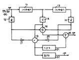
제 3 도는 2H형 콤필터를 사용한 종래의 칼라TV 신호처리 블럭도로서, 단자(102)로 입력되는 복합 영상신호(CVS)를 수평기간(lH) 동안 지연출력하는 1H지연회로(11)와, 상기 lH지연회로(11)의 출력을 1수평기간 동안 지연출력하는 1H지연회로(13)와, 상기 1H지연회로(11)의 입력단자 및 출력단자에 각각 접속되어 입력되는 복합 영상신호를 각각 1/4과 1/2로 축소 출력하는 스케일러(scaaler)(12)(14)와, 상기 1H지연기(13)의 출력단자에 접속되어 지연된 복합 영상신호를 1/4로 축소 출력하는 스케일러(15)와, 상기한 3개의 스케일러(12)(14)(15)로부터 각각 축소 출력되는 신호를 가산 출력하는 가산기(16)와, 상기한 스케일러(12)와 (15)의 출력을 위상 반전하는 반전기(17) 및 (20)과, 상기 반전기(17) 및 (20)의 출력과 상기 스케일러(14)의 출력을 가산하여 출력하는 가산기(19)와, 상기 가산기(19)의 출력을 저역 필터링하여 휘도신호 대역신호만을 출력하는 저역 필터(LPF)(21)와, 상기 가산기(16)의 출력과 상기 저역 통과필터(21)의 출력을 가산하여 휘도신호(Y)를 단자(104)로 출력하는 가산기(18)와, 상기 가산기(19)의 출력을 대역 통과필터링하여 색신호 대역만 출력하는 대역 통과필터(22)로 구성되어 있었다.3 is a conventional color TV signal processing block diagram using a 2H type comb filter, which includes a
상기 제 1 도 및 제 2 도와 같이 구성된 내용의 1H형 콤필터와 2H형 콤필터를 사용하여 휘도신호(Y)와 색신호(C)를 분리하는 경우에는 휘도신호의 대역이 넓어져서 해상도가 증가하게 되어 휘도와 색신호의 간섭현상인 크로스 칼라(Cross Color)를 경감할 수가 있있다. 그러나 상기 제 2 도 및 제 3 도와 같은 회로로서는 후술하는 제 6 도(b)와 같이 수직방향으로 급격히 변화하는 신호에 대하여 휘도신호 대역(채널)에 색부반송파 주파수인 3.58MHz의 도트 방해가 발생하게 되어 문자표시와 같은 경우에는 시청자의 눈에 매우 거슬리게 되는 문제점이 있었다.When the luminance signal (Y) and the color signal (C) are separated by using the 1H type comb filter and the 2H type comb filter configured as shown in FIGS. 1 and 2, the bandwidth of the luminance signal is widened to increase the resolution. Therefore, cross color, which is a phenomenon of interference between luminance and color signals, can be reduced. However, in the circuits shown in Figs. 2 and 3, as shown in Fig. 6 (b) to be described later, a dot interference of 3.58 MHz, which is a color subcarrier frequency, is generated in the luminance signal band (channel) for a signal rapidly changing vertically. In the case of text display, there is a problem that is very annoying to the viewer.
실제적으로 콤필터를 사용하여 색신호를 분리처리시 휘도신호 해상도가 향상된 이상으로 상기와 같은 3.58MHz 도트 방해는 눈에 거슬리게 된다.In practice, the above-mentioned 3.58 MHz dot interference is unobtrusive because the luminance signal resolution is improved when the color signal is separated using the comb filter.
따라서 본 발명의 목적은 색신호 트랩회로 및 색신호 대역 통과필터를 사용하는 칼라텔레비죤 휘도신호/색신호 처리회로에 있어서, 상기 색신호 대역 통과필터 출력단에 크로마 콤필터(Chroma COMB Filter)를 접속하여 색신호 대역에서 발생하는 크로스 칼라를 경감도록 하는 회로를 제공함에 있다.Accordingly, an object of the present invention is to generate a color signal in a color signal band by connecting a chroma comb filter to a color signal band pass filter output terminal in a color television luminance signal / color signal processing circuit using a color signal trap circuit and a color signal band pass filter. It is to provide a circuit for reducing the cross collar.
본 발명의 또다른 목적은 색신호 대역만을 필터링 출력하는 색신호 대역 통과필터로부터 출력되는 색신호에 포함되는 휘도신호 성분을 제거하는 크로마 콤필터를 제공함에 있다.Still another object of the present invention is to provide a chroma comb filter for removing luminance signal components included in a color signal output from a color signal band pass filter that filters and outputs only a color signal band.
이하 본 발명을 첨부한 도면을 참조하여 상세히 설명한다.Hereinafter, the present invention will be described in detail with reference to the accompanying drawings.
제 4 도는 본 발명에 따른 회로도로서, 복합 영상신호(CVS)를 입력하여 완충하고 버퍼링하기 위한 영상버퍼(100)와, 상기 영상버퍼(100)에서 출력되는 복합 영상신호(CVS)를 지연출력하는 지연회로(200)와, 상기 지연회로(200)을 통해 지연입력되는 복합 영상신호중에 포함된 3.579545MHz의 색부반송파(3.58MHz Dot 방해신호)를 제거하기 위한 색부반송파 트랩회로(300)과, 상기 복합 영상신호를 입력하여 색신호 대역만 통과시키어 출력하는 색신호 대역 통과필터(400)와, 상기 색신호 대역 통과필터(400)에서 통과된 3.58MHz의 색부반송파와 3.58MHz 대역의 휘도신호를 입력하여 1수평기간(lH)지연 출력하는 1H지연기(500)와, 상기 1H지연기(500)의 출력을 반전 출력하는 반전기(600)와, 상기 색신호 대역 통과필터(400)에서 출력된 신호와 반전기(600)에서 출력된 신호를 입력하여 가산 출력하는 가산기(700)로 구성된 1H 크로마 콤필터(800)로 구성된다.4 is a circuit diagram according to an embodiment of the present invention, which delays and outputs a
상기한 제 4 도의 구성중 미설명 참조번호 102, 104, 106은 제 1 도에서 전술한 바와 동일한 단자로서, 102는 복합영상신호(CVS)입력단자, 104는 휘도신호(Y)출력단자, l06은 색신호(C)출력단자이고, 108은 1H 크로마 콤필더(800)에서 콤필터링 동작하여 3.58MHz대역의 휘도신호가 제거된 색신호만을 출력하는 단자로서 ACC 및 색복조회로(도시하지 않음)에 접속되는 단자이다.In the configuration of FIG. 4,
한편 제 5 도는 제 4 도의 1H 크로마 콤필터(800)를 대치하기 위한 2H 크로마 콤필터로 색신호 대역 통과 필터(400)에서 출력되는 신호를 위상 반전하고

제 6 도(a)(b)도는 복합 영상신호에서의 색부반송파 위상관계도로서,(a)도는 인접한 두 수평라인의 색상이 같은 경우로서 n번째라인과 n+1번째 라인의 색상이 같은 경우의 위상 관계도로서 매 수평라인마다 색부반송파의 위상이 반전되고 있음을 나타낸 것이다.FIG. 6 (a) (b) is a color carrier phase relationship diagram of a composite video signal, and (a) is a case where two adjacent horizontal lines have the same color, and the colors of the nth line and the n + 1th line are the same. This is a phase relation diagram of which indicates that the phase of the color carrier is inverted in every horizontal line.
(b)도는 인접한 두 수평라인의 색상이 다른 경우로서 n번째 라인에는 색상이 있고 n+1번째 라인에는 색상이 없는 경우로서 수직방향으로 급격히 변화하는 예이다. 이때 상기 제 6 도(a)(b) 도중에서 (a)와(a')는 n번째 수평라인의 색부반송파의 위상이며, (b)와 (b')는 n+1번째 수평라인의 색부반송파 위상이다.(b) is a case where two adjacent horizontal lines have different colors, and there is a color in the nth line and no color in the n + 1th line. (A) and (a ') are phases of the color subcarriers of the nth horizontal line, and (b) and (b') are the colors of the n + 1th horizontal line. Subcarrier phase.
제 7(a)(b) 도는 상기 제 4 도에 의한 휘도신호와 색신호의 주파수 특성도이다.7 (a) (b) are frequency characteristic diagrams of the luminance signal and the color signal according to FIG.
이하 본 발명을 상술한 구성과 도면을 참조하여 상세히 설명한다.Hereinafter, the present invention will be described in detail with reference to the above-described configuration and drawings.
복합 영상신호가 단자(102)을 통해 영상버퍼(100)와 색신호 대역 통과필터(400)로 각각 입력되면, 상기영상버퍼(l00)는 이를 완충하여 출력한다. 상기 영상버퍼(100)에서 완충된 신호는 지연회로(200)를 통해 소정 지연된 후 색부반송파 트랩회로(300)에 입력된다.When the composite video signal is input to the
따라서 색부반송파 트랩회로(300)은 휘도신호 대역에 포함되는 색부반송파(fsc)의 주파수 신호인 3.58MHz 대역 색신호를 제거하여 제 7a 도와 같은 주파수 대역의 휘도신호(Y)을 출력한다.Therefore, the color carrier
따라서 휘도신호(Y) 대역에 포함되는 3.58MHz의 도트방해가 제거된다. 이때 상기 제 7a 도와 같은 주파수 특성을 가지는 색부반송파 트랩회로(300)에 의해 색부반송파 대역(fsc)의 휘도신호 성분을 이용할수 없으므로 해서 해상도의 저하를 가져오게 되나, 실제 소형 칼라텔레비죤에서 영상을 재생할 경우 이 대역의 휘도신호(Y)주파수 성분은 화질에 거의 영향을 미치지 않음을 알 수 있다. 이때 상기 지연회로(200)은 후술하는 색신호 대역 통과필터(400)에서 색신호를 필터링하는 시간을 보상하기 위한 것이다.Therefore, the dot interference of 3.58 MHz included in the luminance signal Y band is eliminated. In this case, since the luminance signal component of the color carrier band fsc cannot be used by the color carrier
한편 복합 영상신호(CVS)를 입력한 색신호 대역 통과필터(400)은 상기 복합 영상신호(CVS)중 3.58MHz의 색신호 대역의 주파수만을 필터링하여 가산기(700)와 1H지연기(500)로 각각 입력시킨다.On the other hand, the color
따라서 1H지연기(500)와 가산기(700)에 입력되는 신호는 상기 색신호 대역 통과필터(400)에서 대역 통과필터링하는 3.58MHz 대역의 색부반송파(fsc)와 3.58MHz대역 성분의 휘도신호가 포함된 신호임을 알 수있다. 이때 인접하는 두 수평라인의 색상이 같은 경우 상기 색신호 대역 통과필터(400)로부터 출력되는 3.58MHz대역의 색부반송파(fsc)의 위상은 제 6a 도와 같다(NTSC방식의 영상신호는 색신호의 위상이 1수평기간마다 반전됨 ; NTSC인터리빙). 즉, n번째 수평라인의 색신호 위상이 제 6(a) 도 (a)라면 차기의 수평라인인 n+1번째 색신호 위상은 제 6(a) 도 (b)와 같이 위상이 반전되고 있다.Therefore, the signal input to the
따라서 상기한 색신호 대역 통과필터(400)로부터 현재 제 6(a) 도 (a)와 같은 n번째 수평라인의 색부반송파(fsc)가 출력되면 상기 3.58MHz 색부반송파(fsc)의 신호는 1H지연기(500)에 의해 지연되고 반전기(600)에서 반전되어 가산기(700)에 입력된다. 이때 상기 1H지연기(500)에서 n번째 라인의 색부반송파(fsc)을 출력하는 상태에는 색신호 대역 통과필터(400)로부터는 제 6(a) 도 (b)와 같은 위상을 갖는 n+1번째라인의 색부반송파(fsc)를 출력하게 된다.Therefore, when the color subcarrier fsc of the nth horizontal line as shown in FIG. 6 (a) (a) is output from the color signal
따라서 가산기(700)은 현재 수평라인의 색부반송파(fsc)에 상기 1H지연기(500)와 반전기(600)에 의해 1수평기간 지연되고 위상이 반전되어 현재 수평라인의 색부반송파(fsc)의 위상과 동일하게 된 이전 수평라인의 색부반송파(fsc)을 가산하여 출력함으로 단자(108)로부터 출력되는 색부반송파의 신호 진폭은 2배로 되어 출력된다. 즉, 원래의 색부반송파에 1수평기간(lH)동안 지연되고 반전된 이전 수평라인의 색부 반송파신호를 가산함으로써 색부반송파의 진폭은 2배로 되어 도시하지 않은 ACC 및 색복조 회로로 출력된다.Therefore, the
한편 휘도신호의 3.58MHz 성분은 색부반송파와는 달리 매라인마다 동일한 극성(위상)이 나타나므로서 현재 수평라인의 휘도신호에서 1H지연된 휘도신호를 가산하면 휘도신호의 3.58MHz대역의 신호는 없어지게 한다. 즉 NTSC방식의 경우 휘도신호의 위상은 색부반송파(fsc)와는 달리 매 수평라인마다 동일위상을가지고 있다. 따라서 전술한 1H지연기(500)에서 1수평기간(lH) 지연된 후 반전기(600)에서 위상이 반전되면, 가산기(700)에 입력되는 신호는 현재 라인의 3.58MHz성분의 휘도신호와 1수평기간 지연되어 위상이 반전된 3.58MHz성분의 휘도신호가 됨으로 3.58MHz성분의 휘도신호는 없어지게 된다.Unlike the color carrier, the 3.58MHz component of the luminance signal has the same polarity (phase) in each line, so if the 1H delayed luminance signal is added to the luminance signal of the current horizontal line, the signal in the 3.58MHz band of the luminance signal is lost. do. In other words, in the NTSC system, the phase of the luminance signal has the same phase in every horizontal line, unlike the color carrier fsc. Therefore, if the phase is reversed in the
그러므로 3.58MHz대역의 색부반송파 신호대역에 포함되어 있는 3.58MHz 대역성분의 휘도신호는 1H지연기(500) 및 반전기(600)와 가산기(700)에 의해 제거되어지므로서 3.58MHz 대역의 휘도신호 성분이 색부반송파(fsc)에 영향을 주어 나타내는 크로스칼라의 유발을 방지할 수 있어 화질의 저하를 막을 수 있다.Therefore, the luminance signal of the 3.58 MHz band component included in the color carrier carrier signal band of the 3.58 MHz band is removed by the
색부반송파 트랩(300)에서 출력된 휘도채널의 주파수 특성도를 살펴보면, 3.58MHz 대역의 색부반송파가 제거되어 출력함으로서 휘도신호는 제 7a 도와 같은 주파수의 특성을 갖는것을 알 수 있다. 또 1H지연기(500)와 반전기(600)와 가산기(700)로 구성된 1H 크로마콤필터(800)에 의해 휘도신호의 3.58MHz 대역의 신호는 제거되고 색부반송파가 2배 증폭 출력함으로서 색부반송파(fsc)의 주파수 선택 특성은 제 7b 도와 같은 주파수 특징을 갖게 한다.Looking at the frequency characteristic diagram of the luminance channel output from the
한편 제 4 도의 1H지연기(500)와 인버터(600)와 가산기(700)로 구성된 1H크로마 콤필터를 제 5 도와 같은 2H형 크로마 콤필터로 대치 사용하여도 상기 기술한 바와같은 동작을 한다.On the other hand, the 1H chroma comb filter composed of the
따라서 색부반송파 트랩(300)을 사용하여 휘도신호대역에 포함 입력되는 3.58MHz의 색부반송파 신호를 제거하여 휘도 신호만을 출력하고, lH크로마 콤필터(800)를 색신호 대역 통과필터(400)의 출력단에 접속하여 3.58MHz대역 부근의 휘도신호를 제거하여 크로스칼라를 제거함으로서 휘도신호와 색신호간 상호간섭을 주는것을 제거할 수 있게 됨을 알 수 있다.Therefore, the
상술한 바와같이 본 발명은 휘도신호와 색신호의 정확한 분리를 위하여 휘도채널에는 색부 반송파 트랩을, 칼라 채널에는 1H크로마 콤필터를 사용함으로서 휘도신호가 색신호에 간섭을 주는것을 제거할 수 있어서 크로스 칼라가 없는 고화질을 얻을 수 있는 이점이 있다.As described above, the present invention can remove the interference of the luminance signal to the color signal by using the color carrier carrier trap for the luminance channel and the 1H chroma comb filter for the color channel for accurate separation of the luminance signal and the color signal. There is an advantage to get high picture quality.
Claims (1)
Translated fromKoreanPriority Applications (1)
| Application Number | Priority Date | Filing Date | Title |
|---|---|---|---|
| KR1019860011759AKR900004035B1 (en) | 1986-12-31 | 1986-12-31 | Luminance and Color Signal Reduction Reduction Circuit in Color Television Receiver |
Applications Claiming Priority (1)
| Application Number | Priority Date | Filing Date | Title |
|---|---|---|---|
| KR1019860011759AKR900004035B1 (en) | 1986-12-31 | 1986-12-31 | Luminance and Color Signal Reduction Reduction Circuit in Color Television Receiver |
Publications (2)
| Publication Number | Publication Date |
|---|---|
| KR880008629A KR880008629A (en) | 1988-08-31 |
| KR900004035B1true KR900004035B1 (en) | 1990-06-09 |
Family
ID=19254749
Family Applications (1)
| Application Number | Title | Priority Date | Filing Date |
|---|---|---|---|
| KR1019860011759AExpiredKR900004035B1 (en) | 1986-12-31 | 1986-12-31 | Luminance and Color Signal Reduction Reduction Circuit in Color Television Receiver |
Country Status (1)
| Country | Link |
|---|---|
| KR (1) | KR900004035B1 (en) |
- 1986
- 1986-12-31KRKR1019860011759Apatent/KR900004035B1/ennot_activeExpired
Also Published As
| Publication number | Publication date |
|---|---|
| KR880008629A (en) | 1988-08-31 |
Similar Documents
| Publication | Publication Date | Title |
|---|---|---|
| US4179705A (en) | Method and apparatus for separation of chrominance and luminance with adaptive comb filtering in a quadrature modulated color television system | |
| SU1158056A3 (en) | Television signal processing device | |
| US4223340A (en) | Image detail improvement in a vertical detail enhancement system | |
| US5519454A (en) | Luma/chroma separation filter with common delay element for comb filter separation and recursive noise reduction of composite video input signal | |
| US4809060A (en) | Hanging dot reduction arrangement | |
| US5448305A (en) | Comb filter capable of reducing cross-color phenomena and noises | |
| KR930003178B1 (en) | Correlated Adaptive Luminance Signal and Color Signal Separation Circuit | |
| US4597007A (en) | Circuitry for correcting frame combed luminance signal for motion induced distortion | |
| CN85108895A (en) | Video signal processing device | |
| JP2578338B2 (en) | Television equipment | |
| EP0464879B1 (en) | Apparatus for separating luminance and chrominance signals and the method thereof | |
| KR900004035B1 (en) | Luminance and Color Signal Reduction Reduction Circuit in Color Television Receiver | |
| US4750033A (en) | Comb filter, chrominance and luminance signal separating circuit for modifying the level-frequency characteristic of the luminance signal | |
| CA1219343A (en) | Apparatus for reducing motion induced distortion in a frame combed chrominance signal | |
| JPS6226996A (en) | Luminance/chrominance signal component separation device | |
| KR20050090005A (en) | Method and device for separating a chrominance signal from a composite video base-band signal | |
| JP3428148B2 (en) | Filter circuit | |
| JP2698637B2 (en) | Luminance signal / chrominance signal separation circuit | |
| KR880000842B1 (en) | Luminance / Color Signal Separation Method | |
| JP2647652B2 (en) | Chroma signal processing circuit | |
| KR940010243B1 (en) | Comb filter for color tv receiver | |
| JPH04252589A (en) | Y/c separator | |
| JP2649254B2 (en) | FM transmission receiver for color television signal | |
| JPH0463089A (en) | Y/C separation circuit | |
| JPH029515B2 (en) |
Legal Events
| Date | Code | Title | Description |
|---|---|---|---|
| A201 | Request for examination | ||
| PA0109 | Patent application | St.27 status event code:A-0-1-A10-A12-nap-PA0109 | |
| PA0201 | Request for examination | St.27 status event code:A-1-2-D10-D11-exm-PA0201 | |
| R17-X000 | Change to representative recorded | St.27 status event code:A-3-3-R10-R17-oth-X000 | |
| P11-X000 | Amendment of application requested | St.27 status event code:A-2-2-P10-P11-nap-X000 | |
| P13-X000 | Application amended | St.27 status event code:A-2-2-P10-P13-nap-X000 | |
| PG1501 | Laying open of application | St.27 status event code:A-1-1-Q10-Q12-nap-PG1501 | |
| E902 | Notification of reason for refusal | ||
| PE0902 | Notice of grounds for rejection | St.27 status event code:A-1-2-D10-D21-exm-PE0902 | |
| T11-X000 | Administrative time limit extension requested | St.27 status event code:U-3-3-T10-T11-oth-X000 | |
| P11-X000 | Amendment of application requested | St.27 status event code:A-2-2-P10-P11-nap-X000 | |
| P13-X000 | Application amended | St.27 status event code:A-2-2-P10-P13-nap-X000 | |
| G160 | Decision to publish patent application | ||
| PG1605 | Publication of application before grant of patent | St.27 status event code:A-2-2-Q10-Q13-nap-PG1605 | |
| E701 | Decision to grant or registration of patent right | ||
| PE0701 | Decision of registration | St.27 status event code:A-1-2-D10-D22-exm-PE0701 | |
| GRNT | Written decision to grant | ||
| PR0701 | Registration of establishment | St.27 status event code:A-2-4-F10-F11-exm-PR0701 | |
| PR1002 | Payment of registration fee | St.27 status event code:A-2-2-U10-U11-oth-PR1002 Fee payment year number:1 | |
| PR1001 | Payment of annual fee | St.27 status event code:A-4-4-U10-U11-oth-PR1001 Fee payment year number:4 | |
| PR1001 | Payment of annual fee | St.27 status event code:A-4-4-U10-U11-oth-PR1001 Fee payment year number:5 | |
| PR1001 | Payment of annual fee | St.27 status event code:A-4-4-U10-U11-oth-PR1001 Fee payment year number:6 | |
| PR1001 | Payment of annual fee | St.27 status event code:A-4-4-U10-U11-oth-PR1001 Fee payment year number:7 | |
| PR1001 | Payment of annual fee | St.27 status event code:A-4-4-U10-U11-oth-PR1001 Fee payment year number:8 | |
| PR1001 | Payment of annual fee | St.27 status event code:A-4-4-U10-U11-oth-PR1001 Fee payment year number:9 | |
| FPAY | Annual fee payment | Payment date:19970829 Year of fee payment:10 | |
| PR1001 | Payment of annual fee | St.27 status event code:A-4-4-U10-U11-oth-PR1001 Fee payment year number:10 | |
| R18-X000 | Changes to party contact information recorded | St.27 status event code:A-5-5-R10-R18-oth-X000 | |
| PN2301 | Change of applicant | St.27 status event code:A-5-5-R10-R13-asn-PN2301 St.27 status event code:A-5-5-R10-R11-asn-PN2301 | |
| PN2301 | Change of applicant | St.27 status event code:A-5-5-R10-R13-asn-PN2301 St.27 status event code:A-5-5-R10-R11-asn-PN2301 | |
| LAPS | Lapse due to unpaid annual fee | ||
| PC1903 | Unpaid annual fee | St.27 status event code:A-4-4-U10-U13-oth-PC1903 Not in force date:20000610 Payment event data comment text:Termination Category : DEFAULT_OF_REGISTRATION_FEE | |
| R18-X000 | Changes to party contact information recorded | St.27 status event code:A-5-5-R10-R18-oth-X000 | |
| PC1903 | Unpaid annual fee | St.27 status event code:N-4-6-H10-H13-oth-PC1903 Ip right cessation event data comment text:Termination Category : DEFAULT_OF_REGISTRATION_FEE Not in force date:20000610 | |
| PN2301 | Change of applicant | St.27 status event code:A-5-5-R10-R13-asn-PN2301 St.27 status event code:A-5-5-R10-R11-asn-PN2301 | |
| R18-X000 | Changes to party contact information recorded | St.27 status event code:A-5-5-R10-R18-oth-X000 | |
| R18-X000 | Changes to party contact information recorded | St.27 status event code:A-5-5-R10-R18-oth-X000 | |
| R18-X000 | Changes to party contact information recorded | St.27 status event code:A-5-5-R10-R18-oth-X000 | |
| PN2301 | Change of applicant | St.27 status event code:A-5-5-R10-R13-asn-PN2301 St.27 status event code:A-5-5-R10-R11-asn-PN2301 | |
| PN2301 | Change of applicant | St.27 status event code:A-5-5-R10-R13-asn-PN2301 St.27 status event code:A-5-5-R10-R11-asn-PN2301 | |
| R18-X000 | Changes to party contact information recorded | St.27 status event code:A-5-5-R10-R18-oth-X000 | |
| P22-X000 | Classification modified | St.27 status event code:A-4-4-P10-P22-nap-X000 |